EP1659636B1 - MOS-Leistungshalbleiteranordnung - Google Patents
MOS-Leistungshalbleiteranordnung Download PDFInfo
- Publication number
- EP1659636B1 EP1659636B1 EP05025285A EP05025285A EP1659636B1 EP 1659636 B1 EP1659636 B1 EP 1659636B1 EP 05025285 A EP05025285 A EP 05025285A EP 05025285 A EP05025285 A EP 05025285A EP 1659636 B1 EP1659636 B1 EP 1659636B1
- Authority
- EP
- European Patent Office
- Prior art keywords
- resistance
- realised
- islands
- gate
- strips
- Prior art date
- Legal status (The legal status is an assumption and is not a legal conclusion. Google has not performed a legal analysis and makes no representation as to the accuracy of the status listed.)
- Expired - Lifetime
Links
Images


Classifications
-
- H—ELECTRICITY
- H10—SEMICONDUCTOR DEVICES; ELECTRIC SOLID-STATE DEVICES NOT OTHERWISE PROVIDED FOR
- H10D—INORGANIC ELECTRIC SEMICONDUCTOR DEVICES
- H10D30/00—Field-effect transistors [FET]
- H10D30/60—Insulated-gate field-effect transistors [IGFET]
- H10D30/64—Double-diffused metal-oxide semiconductor [DMOS] FETs
- H10D30/66—Vertical DMOS [VDMOS] FETs
-
- H—ELECTRICITY
- H10—SEMICONDUCTOR DEVICES; ELECTRIC SOLID-STATE DEVICES NOT OTHERWISE PROVIDED FOR
- H10D—INORGANIC ELECTRIC SEMICONDUCTOR DEVICES
- H10D64/00—Electrodes of devices having potential barriers
- H10D64/60—Electrodes characterised by their materials
- H10D64/66—Electrodes having a conductor capacitively coupled to a semiconductor by an insulator, e.g. MIS electrodes
- H10D64/661—Electrodes having a conductor capacitively coupled to a semiconductor by an insulator, e.g. MIS electrodes the conductor comprising a layer of silicon contacting the insulator, e.g. polysilicon having vertical doping variation
- H10D64/662—Electrodes having a conductor capacitively coupled to a semiconductor by an insulator, e.g. MIS electrodes the conductor comprising a layer of silicon contacting the insulator, e.g. polysilicon having vertical doping variation the conductor further comprising additional layers, e.g. multiple silicon layers having different crystal structures
- H10D64/663—Electrodes having a conductor capacitively coupled to a semiconductor by an insulator, e.g. MIS electrodes the conductor comprising a layer of silicon contacting the insulator, e.g. polysilicon having vertical doping variation the conductor further comprising additional layers, e.g. multiple silicon layers having different crystal structures the additional layers comprising a silicide layer contacting the layer of silicon, e.g. polycide gates
-
- H—ELECTRICITY
- H10—SEMICONDUCTOR DEVICES; ELECTRIC SOLID-STATE DEVICES NOT OTHERWISE PROVIDED FOR
- H10D—INORGANIC ELECTRIC SEMICONDUCTOR DEVICES
- H10D64/00—Electrodes of devices having potential barriers
- H10D64/60—Electrodes characterised by their materials
- H10D64/66—Electrodes having a conductor capacitively coupled to a semiconductor by an insulator, e.g. MIS electrodes
- H10D64/671—Electrodes having a conductor capacitively coupled to a semiconductor by an insulator, e.g. MIS electrodes the conductor having lateral variation in doping or structure
-
- H—ELECTRICITY
- H10—SEMICONDUCTOR DEVICES; ELECTRIC SOLID-STATE DEVICES NOT OTHERWISE PROVIDED FOR
- H10D—INORGANIC ELECTRIC SEMICONDUCTOR DEVICES
- H10D64/00—Electrodes of devices having potential barriers
- H10D64/20—Electrodes characterised by their shapes, relative sizes or dispositions
- H10D64/27—Electrodes not carrying the current to be rectified, amplified, oscillated or switched, e.g. gates
- H10D64/311—Gate electrodes for field-effect devices
- H10D64/411—Gate electrodes for field-effect devices for FETs
- H10D64/511—Gate electrodes for field-effect devices for FETs for IGFETs
- H10D64/517—Gate electrodes for field-effect devices for FETs for IGFETs characterised by the conducting layers
- H10D64/519—Gate electrodes for field-effect devices for FETs for IGFETs characterised by the conducting layers characterised by their top-view geometrical layouts
Definitions
- the present invention relates to a power electronic device, such as a MOS device of the type comprising a very high integration of elementary MOS transistors and used in multiple applications both at low and high supply voltage.
- the invention particularly, relates to a power MOS device and the following description is made with reference to this field of application by way of illustration only.
- MOS devices in fact require the possibility of operating, both at low supply voltage (20-100V) and at high supply voltage (200-1000V), but, however, at higher and higher frequencies next to the megahertz (MHz).
- Power devices are thus subjected to very high voltage and current gradients during the transients and/or during the switch steps which make the stresses to the device weakening the same burdensome and reduce its activity period in a drastic way.
- elementary MOS transistors are realised on semiconductor or with polygonal cells or strips and they comprise a body region, which, in the case shown, is of the p type, formed on a suitable substrate, of the n type, and with a source region realised on top.
- the body region together with the source region, forms a channel region covered by an insulating layer, for example a silicon oxide, and by a conductive layer, for example suitably doped polysilicon.
- an insulating layer for example a silicon oxide
- a conductive layer for example suitably doped polysilicon.
- These two insulating and conductive layers represent, for each elementary MOS transistor, the gate dielectric and for the power MOS device they form a biasing mesh also called gate mesh.
- the gate mesh is connected to a terminal called gate pad and it allows to distribute the signals inside the MOS device as well as to turn on and/or off all the elementary MOS transistors composing the power MOS device.
- the gate mesh due to the high polysilicon resistivity (> 10 Ohm/square), exhibits resistive contributions along the path which depend on the relative position with respect to the gate pad, as highlighted in the circuit of figure 2 , this implies that gate resistance value of each elementary transistor also depends on the distance from the gate pad.
- each elementary MOS transistor responds with a time constant which will be distinct, being, as known, a function of the input capacity and of the gate resistance.
- the gate resistance is thus an important value because, together with the input capacity of the MOS device, forms an RC circuit whose time constant is one of the most important parameters influencing the switch speed of power MOS devices. These latter, having to operate at higher and higher frequencies, require a more and more reduced time constant. There is then an attempt to reduce the gate resistance and to make it homogeneous for the entire MOS device so as to ensure a good reliability even at high frequency.
- connection buses also called gate fingers, realised in metallic material, so as to connect the gate pad to various points of the gate mesh by "short-circuiting" them, as shown in figure 3 and in the corresponding circuit of figure 4 .
- a technique is that of increasing the number of gate fingers so as to intersect the gate mesh in the greatest number of points as possible.
- a further known solution to reduce the gate resistance provides the decrease of the gate mesh resistance by integrating there inside a very conductive layer.
- metallic silicides such as for example cobalt silicide (CoSi 2 ), platinum silicide (PtSi), titanium silicide (TiSi 2 ) or tungsten silicide (WSi 2 ), all materials exhibiting a layer resistivity of about a lower magnitude order with respect to that of the polysilicon.
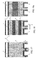
- Figure 5 highlights a pattern in parallel of a pair of elementary MOS transistors which exhibit different gate resistances according to the position wherein they are with respect to the gate pad and to the gate fingers.
- the diagram reported in figure 6 shows how between elementary MOS transistors wherein there exists an unbalance in the resistance value, during the switch step of the MOS device, different wave forms are produced which distribute the current at stake in a non uniform way. In particular it can be verified how the current intensity 12 crossing the slowest component, undergoes sudden increases negatively affecting the uniformity of the time constant of the MOS device.
- the power MOS device obtained will exhibit areas with different distances between the gate fingers, as shown in the example of figure 8 , and this implies the presence of a gate resistance influenced by the area with shortest distance between the gate fingers, since in the calculation of the parallel the areas with higher resistance will have less weight.
- the areas in correspondence with the points A and B although being near the gate finger exhibit a different resistance in series due to the contribution of the gate finger section AB, which could have an even higher weight than one Ohm, with a consequent unbalance between the different areas of the power MOS device.
- a width of the metallic tracks of the gate finger equal to 10-50 ⁇ m
- a thickness of the metallic layer between 2-10 ⁇ m and fixing at 5mm the width of an aluminium track the values of the minimum resistance of the gate finger will be equal to 0,3 Ohm and the highest equal to 7 Ohm.
- the unbalance can also cause current focalisations which can cause the non correct operation and/or the breaking of the power MOS device.
- the technical problem underlying the present invention is that of devising a power MOS device with a high integration density, comprising a plurality of elementary MOS transistors and with such a gate structure as to ensure a uniform resistance and thus a controlled switch and a simultaneous time constant, exhibiting in the meantime such structural and functional characteristics as to allow to overcome the drawbacks cited with reference to the prior art.
- Another aim of the invention is that of uniforming the gate resistance seen from each elementary MOS as much as possible.
- the solution idea underlying the present invention is that of realising a power MOS device comprising a plurality of elementary MOS transistors and a gate structure realised with a conductive material with programmable resistivity exhibiting a plurality of independent islands, suitably distributed and localised.
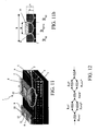
- the device 1 comprises a plurality of elementary MOS transistors 2, arranged in parallel to each other, realised on a silicon plate comprising a semiconductor layer 4 overlapped onto a substrate 3.
- the layer 4 exhibits a first type of conductivity which, in the case highlighted in the figure, is of the N- type while the substrate 3 is of the N+ type with increased doping.
- the elementary MOS transistors 2 shown in the figures are realised only by way of indication with strip-like structures, even if the present invention can be applied on devices with elementary MOS transistors with cellular structure.
- the elementary MOS transistors 2 exhibit a body region 5, realised with a second type of conductivity, a source region 6 contained above such body region 5 and an overlying gate oxide 7 which partially covers the body 5 and the source region 6 to define an underlying channel region 7a.
- the MOS device 1 exhibits a gate structure 12 comprising a plurality of strips 8 realised with a first conductive material, such as for example polysilicon, arranged above the gate oxide 7 and self-aligned thereto.
- a first conductive material such as for example polysilicon
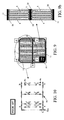
- the strips 8, according to a standard layout, can be directly connected to a gate pad 30, suitably provided on the upper surface of the MOS device 1, or they can be connected thereto by means of a plurality of gate fingers or metallic tracks 11.
- the gate fingers 11, where present, are realised in particularly conductive material, such as a metal, and they thus allow to quickly transfer each signal coming from the gate pad 30 directly to the plurality of conductive strips 8 and thus to the single elementary MOS transistors 2 electrically connected.
- connection layer 20 also preferably realised with a conductive material, such as for example polysilicon.
- This connection conductive layer 20 introduces a further resistive contribution (Ra) in series to the conductive strips 8 ( fig. 10 ) whose value depends on the number and on the dimensions of the islands 10.
- the gate structure 12 has programmable resistivity and it comprises a plurality of islands 10 realised with at least a second conductive material having a different resistivity than that of the first conductive material.
- the plurality of islands 10 are formed on an upper surface 9 of said conductive strips 8.
- the plurality of islands 10 is realised for example with a metallic silicide or by means of ionic implantation of doping species.
- these islands can be realised by means of selective silicidation of the polysilicon.
- a further realisation could however provide that a group of islands 10, or each island 10 of said plurality, can be realised with a conductive material different from another group or from another island 10.
- Each island 10 exhibits, in plan, a polygonal conformation. In the preferred embodiment shown in figure 11 each island 10 has a rectangular conformation.
- the plurality of islands 10 formed on the upper surface 9 of the strip 8 are aligned along such conductive strip 8 and they exhibit realisation parameters of length Co, of width X and of distance p from the preceding which, although varying, meet some relations as better specified hereafter.
- the depth of these islands 10 depends on the formation process and it is a fix parameter inside the device.
- the plurality of islands 10 formed on the upper surface 9 allow to create resistances of suitable value to be connected in series and/or in parallel to the conductive strips 8 to compensate their resistive values.
- Each island 10 formed on the upper surface 9 of the strip 8 projects therefrom, as shown in the section of figure 11b and it leans on a polysilicon layer.
- each island 10 can be completely contained in the polysilicon layer or wrapped by the polysilicon layer of the conductive strip 8 with an upper surface coplanar with the surface 9 of the strip 8 or realised on the surface 9 of the strip 8.
- the values of such realisation parameters of the islands 10 will have to be compatible with the technology used and the equipments employed.
- the conductive material with which the islands 10 can be realised can vary according to the specific needs, being for example cobalt silicide (CoSi 2 ), platinum silicide (PtSi), titanium silicide (TiSi 2 ) or tungsten silicide (WSi 2 ).
- the islands 10 can be realised also by means of selective ionic implantation of doping species which change the resistivity of the polysilicon layer 8 inside the island 10.
- the determinant fact for the invention is that the islands 10 have a different resistivity with respect to the remaining parts 15 of the conductive strip 8.
- the conductive strip 8 with programmable resistivity will have first portions 15 realised in a polysilicon layer alternative with second portions 16 realised by a polysilicon layer and with a silicide layer which defines the island 10.
- the resistance of a conductive strip 8 has an equivalent circuit reported in figure 12 and it is considered as a series n, where n is the number of islands (10) suitably formed in said conductive strip (8), of polysylicon resistances R poly 1,2,..n of the first portions 15 alternated with polysilicon resistances R poly 1a,2a,...na in parallel with silicide resistances R sil 1,2,...n of the second portions 16.
- each conductive strip 8 influences the time constant of the elementary MOS transistors 2 electrically connected to the strip 8 and in particular the response of the MOS device 1 to each signal coming from the gate pad 30 is influenced.
- the values of the realisation parameters of the islands 10 will be predefined so that each conductive strip 8 responds to each signal coming from the gate pad 30 with a same time constant.
- time constant of a conductive strip 8 of length L is equal to (rL)*(cL) where r and c are respectively unitary resistance and capacity of the strip 8.
- the unitary capacity c depends on the width s of the conductive strip 8 and on the thickness of the underlying gate oxide 7 and it is thus a constant according to the technologies used, in particular it will be independent from the islands 10 introduced.
- the time constant of the MOS device 1 can be corrected to ratios meeting the following relation: L max L ⁇ r p r max
- L max /L values which allow to obtain a good definition of the time constant and thus of the response of the power MOS device 1 to the external stresses.
- the islands 10 can have correlated realisation parameters and variable arrangements.
- the islands 10 can be contiguous with at least one attached side, thus forming a continuous strip 25 along the conductive strip 8.
- variable dimensional parameter of each island 10 is the width X of the continuous strip 25.
- the unitary resistance r is given by the parallel between:
- the power MOS device 1 in the case shown in figure 9 exhibits the three gate fingers 11 which, being realised as metallic tracks, add resistances (Rb in fig. 10 ) in series to the resistances of the conductive strips 8 which can, separately according to their dimensions, introduce, according to prior art, resistance values equal to 0,3-7 Ohm.
- a second aim of the present invention is that of compensating the effect of this contribution of each gate finger 11 so as to uniform the resistive contribution seen from all the series of elementary MOS (strip 8) connected thereto.
- resistances (Ra(x)) are realised whose value depends on the distance x from the gate pad or from the start of the gate finger ( fig. 15a).
- Figure 15c reports a block equivalent electric scheme of the device of figure 15 wherein the resistances of the gate fingers (Rb) and the additional ones of the connection layer 20 are highlighted whose value depends on the position.
- Such resistances also called balance resistances and realised in the connection layer 20, allow to compensate the different resistive contribution of the gate fingers 11 according to the distance x from the gate pad 30.
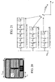
- variable resistances Ra(x) are realised in the connection layer 20 by introducing islands 10 with different resistivity with respect to the remaining conductive area. These islands can have different shapes as shown, only by way of example, in the series of figures 17, 18 and 19 .
- the determinant characteristic is that one or more geometric parameters can vary according to the distance x influencing, in a known way, the resistive contribution Ra(x).
- figure 15 shows a layout of a power MOS device 1 comprising a gate pad 30 connected to two vertical arms 13 with resistance R1 and R2, two external gate fingers 11 and an inner one whose incremental resistances are indicated as R b .
- the total value of the resistances, R b depends on the distance x from a reference which can be the gate pad 30 or an edge to which respect the gate pad 30 is realised.
- the reference is the left edge of the plate whereon the power MOS device 1 is realised.
- connection layer 20 varies when the distance x varies.
- Ra(x) indicates the resistances introduced into the connection layers 20 with the suitable islands 10 formed therein which allow to compensate the different resistance of the gate finger 11 according to the distance x from the left edge of the plate.
- the value of the resistance Ra(x) is chosen so as to exactly compensate the highest value of the resistive contribution of the gate finger 11, as schematised in the diagram reported in figure 16 .
- R b x is the product between the unitary resistance of the conductive layer forming the gate finger and the distance x from the reference side and it represents the resistive value introduces by the gate finger to that position.
- the resistance value Ra equal to the value of resistance Ra(x) which can be calculated with the above indicated formula according to the distance x, must be realised in series to one or to more conductive strips 8 in correspondence with the connection layer 20.
- the resistance Ra can be realised in the connection layer 20 which connects two strips 8 to the gate finger 11, by means of the formation of two independent islands 10, realised transversally to the connection layer 20 and placed at a distance D.
- the value of Ra can be obtained according to the example indicated in figure 19a .
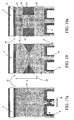
- the islands 10 formed on the upper surface of the connection layer 20 are partially connected to each other to form a structure 21 which exhibits a substantially H-like conformation in plan comprising a central portion 22 and two transversal portions 23.
- the leading idea is that of introducing in the area 20 a resistance whose value varies inside the device so as to compensate the resistive contribution, or better, being dynamic stresses, the impedance introduced by the gate fingers.
- These resistances inside the area 20 can be realised by suitably modifying the shape and/or the number of the islands 10 of conductive material.
- the power MOS device 1, according to the present invention thus allows to realise a gate structure 12, comprising conductive strips 8 and possible structures 20 for connection to the gate fingers 11, with variable resistivity according to the islands 10 being formed which allow to suitably modify the gate global resistivity.
- a further advantage of the present invention is due to the fact that having the gate structure 12 a regulable resistivity, according to the dimensions and the material of the islands 10 formed, it is important to ensure a uniform resistance to each elementary MOS transistor 2 and this allows to uniform the time constant RC of the power MOS device 1 thus ensuring a controlled switch also at high operation frequencies.
- the power MOS device realised by means of the present invention, with a gate structure having programmable resistivity allows to improve and to balance the dynamic response to the signals coming from the gate pad.
Landscapes
- Electrodes Of Semiconductors (AREA)
- Metal-Oxide And Bipolar Metal-Oxide Semiconductor Integrated Circuits (AREA)
Claims (17)
- Leistungs-MOS-Vorrichtung des Typs, die Folgendes aufweist:- eine Mehrzahl elementarer Leistungs-MOS-Transistoren (2) mit einem Körperbereich (5) und einem Sourcebereich (6) über dem Körperbereich (5); und- eine Gate-Struktur (12), die eine Mehrzahl von Streifen (8) aufweist, die mit einem ersten leitfähigen Material realisiert sind;wobei die Gate-Struktur (12) eine Mehrzahl von Inseln (10) aufweist, die mit mindestens einem zweiten leitfähigen Material realisiert sind, das einen anderen spezifischen Widerstand als das erste leitfähige Material aufweist, und die in der Mehrzahl der leitfähigen Streifen (8) hervorstehen,
wobei jeder der leitfähigen Streifen (8) eine Anzahl von n Inseln (10) aufweist und ein Ersatzschaltbild bildet, das durch eine Reihe von ersten Widerstandselementen, die dem ersten leitfähigen Material zugeordnet sind, mit dem die Streifen (8) gebildet sind, und zweiten Widerstandselementen, von denen jedes durch einen zweiten Widerstand gebildet ist, der dem ersten leitfähigen Material entsprechend den Inseln (10) zugeordnet ist, parallel mit einem dritten Widerstand gebildet ist, der dem zweiten leitfähigen Material zugeordnet ist, mit dem die Inseln (10) realisiert sind, wobei die ersten und zweiten Widerstandselemente in der Reihe einander abwechselnd vorgesehen sind,
und wobei die Reihe der Widerstände von Punkt zu Punkt innerhalb der Vorrichtung variiert. - Vorrichtung nach Anspruch 1,
wobei die Inseln (10) in der Draufsicht eine polygonale Gestalt aufweisen. - Vorrichtung nach Anspruch 1,
wobei die Inseln (10) in der Draufsicht eine rechteckige Gestalt aufweisen. - Vorrichtung nach Anspruch 2,
wobei die mehreren Inseln (10) längs des Streifens (8) ausgerichtet sind. - Vorrichtung nach einem der vorausgehenden Ansprüche,
wobei die Inseln (10) zusammenhängend ausgebildet sind und an mindestens einer Seite angebracht sind. - Vorrichtung nach Anspruch 4,
wobei die Inseln (10) mit der mindestens einen angebrachten Seite einen kontinuierlichen Streifen (25) entlang dem leitfähigen Streifen (8) bilden. - Vorrichtung nach Anspruch 2,
wobei jede Insel (10), die auf der oberen Oberfläche (9) ausgebildet ist, die mit dem zweiten leitfähigen Material realisiert ist, Ausbildungsparameter der Länge Co, der Breite X und der Distanz p von der vorhergehenden Insel (10) aufweist, die die Erzeugung eines Widerstands Rsi, zur Verbindung in Reihe und/oder parallel mit durch die leitfähigen Streifen (8) erzeugten Widerständen Rsp ermöglichen. - Vorrichtung nach Anspruch 1,
wobei die leitfähigen Streifen (8) in Polysilizium realisiert sind und erste Bereiche (15), die mit einer einzigen Polysiliziumschicht realisiert sind, abwechselnd mit zweiten Bereichen (16) aufweisen, die mit einer Polysiliziumschicht realisiert sind, die in Überlappung mit der mit einer Silizidschicht gebildeten Insel (10) vorgesehen ist. - Vorrichtung nach Anspruch 7,
wobei die Ausbildungsparameter von jeder Insel (10) der Mehrzahl von Inseln (10) in Beziehung zu den Werten der Längen der leitfähigen Streifen (8) stehen. - Vorrichtung nach Anspruch 7,
wobei die Ausbildungsparameter von jeder Insel (10) der Mehrzahl von Inseln gemäß der nachfolgenden Gleichung in Beziehung zu den Werten der Längen der leitfähigen Streifen (8) stehen:
- Vorrichtung nach Anspruch 6,
wobei die kontinuierlichen Streifen (25) der entlang der leitfähigen Steifen (8) ausgebildeten Inseln (10) eine dimensionsmäßige Breite X in Relation zu der Länge L der Streifen (8) aufweisen. - Vorrichtung nach Anspruch 6,
wobei bei Bezeichnung einer maximalen Länge der Streifen (8) mit Lmax und Bezeichnung einer maximalen Breite des in dem maximalen Streifen (8) ausgebildeten kontinuierlichen Streifens (25) mit Xmax sowie bei Bezeichnung der Länge von einem der leitfähigen Streifen (8) mit L eine Breite eines auf dem Streifen (8) mit der Länge L ausgebildeten kontinuierlichen Streifens (25) folgende Beziehung erfüllt: Rsp den Widerstand des Polysiliziumbereichs;Rspsi den Polysilizium-Widerstand einschließlich des kontinuierlichen Streifens (25);s eine Breite des leitfähigen Streifens (8).
 - Vorrichtung nach Anspruch 12,
wobei der Widerstand Rsp Werte aufweist, die zwischen 30 und 45 Ohm/□ liegen, und wobei der Widerstand Rspsi Werte aufweist, die zwischen 0,5 und 5 Ohm/[] liegen. - Vorrichtung nach einem der vorausgehenden Ansprüche,
aufweisend einen Gate-Anschluss (30) und einen oder mehreren Gate-Finger (11), der bzw. die zum Übertragen von Signalen von dem Gate-Anschluss (30) zu den leitfähigen Steifen (8) mittels einer Verbindung mit einer mit Polysilizium realisierten Verbindungsschicht (20) geeignet sind,
wobei die Verbindungsschicht (20) mindestens eine Insel (10) aufweist, die mit einem zweiten leitfähigen Material realisiert ist. - Vorrichtung nach Anspruch 14,
wobei bei Bezeichnung eines maximalen Widerstands der Gate-Finger (11) mit Rmax und bei Bezeichnung eines zusätzlichen Widerstands der Verbindungsschicht (20), die einen oder mehrere der Inseln (10) aufweist, mit Ra(x) der zusätzliche Widerstand Ra(x) folgende Beziehung erfüllt: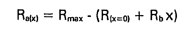 R(x=0) einen Widerstand in Reihe zu jedem der Gate-Finger (11) in Abhängigkeit von der Distanz von dem Gate-Anschluss;Rbx der durch den Gate-Finger (11) eingeführte Widerstand zu einer Distanz x.
 - Vorrichtung nach Anspruch 15,
wobei es sich bei den in der Verbindungsschicht (20) realisierten Inseln (10) um zwei transversal realisierte Inseln handelt, die in einem Abstand D voneinander beabstandet sind, und wobei der zusätzliche Widerstand Ra(x) sich wie folgt ergibt: - L eine Breite und H eine Gesamtlänge der Verbindungsschicht (20);- D den Abstand zwischen den beiden Inseln (10);- Rsp einen Widerstand der Verbindungsschicht (20), die durch eine Schicht ausschließlich mit Polysilizium realisiert ist;- Rspsi einen Widerstand der Verbindungsschicht (20), die durch die Polysiliziumschicht in Überlappung mit den Inseln (10) gebildet ist.
 - Vorrichtung nach Anspruch 15,
wobei die in der Verbindungsschicht (20) realisierten Inseln (10) partiell miteinander verbunden sind, um eine Struktur (21) zu bilden, die eine im Wesentlichen H-förmige Gestalt in der Draufsicht bildet und einen zentralen Bereich (22) sowie zwei transversale Bereiche (23) aufweist, und wobei der zusätzliche Widerstand Ra(x) gleich ist mit: - L eine Breite der Verbindungsschicht (20);- h und b die Höhe und die Breite des zentralen Bereichs (22) der Struktur (21), der in einer Polysiliziumschicht und einer überlappten Silizidschicht realisiert ist und einen Widerstand aufweist, der gleich Rspsi ist;- Rsp einen Widerstand der Verbindungsschicht (20), die in einer einzigen Polysiliziumschicht realisiert ist.
Applications Claiming Priority (1)
| Application Number | Priority Date | Filing Date | Title |
|---|---|---|---|
| IT002245A ITMI20042245A1 (it) | 2004-11-19 | 2004-11-19 | Dispositivo elettronico mos di potenza a commutazione controllata |
Publications (2)
| Publication Number | Publication Date |
|---|---|
| EP1659636A1 EP1659636A1 (de) | 2006-05-24 |
| EP1659636B1 true EP1659636B1 (de) | 2009-11-04 |
Family
ID=35589628
Family Applications (1)
| Application Number | Title | Priority Date | Filing Date |
|---|---|---|---|
| EP05025285A Expired - Lifetime EP1659636B1 (de) | 2004-11-19 | 2005-11-18 | MOS-Leistungshalbleiteranordnung |
Country Status (3)
| Country | Link |
|---|---|
| EP (1) | EP1659636B1 (de) |
| DE (1) | DE602005017457D1 (de) |
| IT (1) | ITMI20042245A1 (de) |
Families Citing this family (2)
| Publication number | Priority date | Publication date | Assignee | Title |
|---|---|---|---|---|
| US8664713B2 (en) | 2008-12-31 | 2014-03-04 | Stmicroelectronics S.R.L. | Integrated power device on a semiconductor substrate having an improved trench gate structure |
| IT202200014566A1 (it) * | 2022-07-11 | 2024-01-11 | St Microelectronics Srl | Dispositivo mosfet di potenza con struttura di porta isolata migliorata e relativo processo di fabbricazione |
-
2004
- 2004-11-19 IT IT002245A patent/ITMI20042245A1/it unknown
-
2005
- 2005-11-18 EP EP05025285A patent/EP1659636B1/de not_active Expired - Lifetime
- 2005-11-18 DE DE602005017457T patent/DE602005017457D1/de not_active Expired - Lifetime
Also Published As
| Publication number | Publication date |
|---|---|
| DE602005017457D1 (de) | 2009-12-17 |
| ITMI20042245A1 (it) | 2005-02-19 |
| EP1659636A1 (de) | 2006-05-24 |
Similar Documents
| Publication | Publication Date | Title |
|---|---|---|
| US8420487B2 (en) | Power MOS electronic device and corresponding realizing method | |
| US6933563B2 (en) | High performance, integrated, MOS-type semiconductor device and related manufacturing process | |
| US5592006A (en) | Gate resistor for IGBT | |
| US10566324B2 (en) | Integrated gate resistors for semiconductor power conversion devices | |
| KR20090036831A (ko) | 멀티 핑거 트랜지스터 및 그 제조 방법 | |
| US5801091A (en) | Method for current ballasting and busing over active device area using a multi-level conductor process | |
| US5998275A (en) | Method for programmable integrated passive devices | |
| US20100117162A1 (en) | Semiconductor Body and Method for the Design of a Semiconductor Body with a Connecting Line | |
| JP3677346B2 (ja) | 電界効果により制御可能の半導体デバイス | |
| EP0544364B1 (de) | Monolitische Halbleiteranordnung mit vertikaler Struktur die einen Leistungstransistor enthält mit tiefer Base und Finger-Emitter mit Ballastwiderstand | |
| US6140680A (en) | Integrated power semiconductor transistor with current sensing | |
| US5977587A (en) | Semiconductor device and a method for wiring of a semiconductor device | |
| EP1659636B1 (de) | MOS-Leistungshalbleiteranordnung | |
| EP0330299A2 (de) | Teilkundenspezifische integrierte Schaltung | |
| US20050110608A1 (en) | Trimmer impedance component, semiconductor device and trimming method | |
| US7105912B2 (en) | Resistor structure and method for manufacturing the same | |
| EP1618607B1 (de) | Halbleiteranordnung mit einem ldmos feldeffekttransistor und verfahren zum betrieb derselben | |
| EP1659638B1 (de) | MOS-Leistungsanordnung und entsprechendes Herstellungsverfahren | |
| EP1296380B1 (de) | Kondensator mit veränderlicher Kapazität | |
| US20100289087A1 (en) | Semiconductor device and method of manufacturing a semiconductor device | |
| DE102020107747B4 (de) | Transistoranordnung mit einem lasttransistor und einemerfassungstransistor und elektronische schaltung mit dieser | |
| US7923751B2 (en) | Bipolar transistor with a low saturation voltage | |
| US20040067610A1 (en) | RF semiconductor devices and methods for fabricating the same | |
| JP6800026B2 (ja) | 半導体装置及び半導体装置の製造方法 | |
| JP3664907B2 (ja) | パワートランジスタ |
Legal Events
| Date | Code | Title | Description |
|---|---|---|---|
| PUAI | Public reference made under article 153(3) epc to a published international application that has entered the european phase |
Free format text: ORIGINAL CODE: 0009012 |
|
| AK | Designated contracting states |
Kind code of ref document: A1 Designated state(s): AT BE BG CH CY CZ DE DK EE ES FI FR GB GR HU IE IS IT LI LT LU LV MC NL PL PT RO SE SI SK TR |
|
| AX | Request for extension of the european patent |
Extension state: AL BA HR MK YU |
|
| 17P | Request for examination filed |
Effective date: 20061113 |
|
| 17Q | First examination report despatched |
Effective date: 20061215 |
|
| AKX | Designation fees paid |
Designated state(s): DE FR GB IT |
|
| GRAP | Despatch of communication of intention to grant a patent |
Free format text: ORIGINAL CODE: EPIDOSNIGR1 |
|
| GRAS | Grant fee paid |
Free format text: ORIGINAL CODE: EPIDOSNIGR3 |
|
| GRAA | (expected) grant |
Free format text: ORIGINAL CODE: 0009210 |
|
| AK | Designated contracting states |
Kind code of ref document: B1 Designated state(s): DE FR GB IT |
|
| REG | Reference to a national code |
Ref country code: GB Ref legal event code: FG4D |
|
| REF | Corresponds to: |
Ref document number: 602005017457 Country of ref document: DE Date of ref document: 20091217 Kind code of ref document: P |
|
| RAP2 | Party data changed (patent owner data changed or rights of a patent transferred) |
Owner name: STMICROELECTRONICS SRL |
|
| PLBE | No opposition filed within time limit |
Free format text: ORIGINAL CODE: 0009261 |
|
| STAA | Information on the status of an ep patent application or granted ep patent |
Free format text: STATUS: NO OPPOSITION FILED WITHIN TIME LIMIT |
|
| 26N | No opposition filed |
Effective date: 20100805 |
|
| GBPC | Gb: european patent ceased through non-payment of renewal fee |
Effective date: 20100204 |
|
| PG25 | Lapsed in a contracting state [announced via postgrant information from national office to epo] |
Ref country code: GB Free format text: LAPSE BECAUSE OF NON-PAYMENT OF DUE FEES Effective date: 20100204 |
|
| PGFP | Annual fee paid to national office [announced via postgrant information from national office to epo] |
Ref country code: IT Payment date: 20101103 Year of fee payment: 6 |
|
| PG25 | Lapsed in a contracting state [announced via postgrant information from national office to epo] |
Ref country code: IT Free format text: LAPSE BECAUSE OF NON-PAYMENT OF DUE FEES Effective date: 20121118 |
|
| PGFP | Annual fee paid to national office [announced via postgrant information from national office to epo] |
Ref country code: FR Payment date: 20131121 Year of fee payment: 9 Ref country code: DE Payment date: 20131022 Year of fee payment: 9 |
|
| REG | Reference to a national code |
Ref country code: DE Ref legal event code: R119 Ref document number: 602005017457 Country of ref document: DE |
|
| REG | Reference to a national code |
Ref country code: FR Ref legal event code: ST Effective date: 20150731 |
|
| PG25 | Lapsed in a contracting state [announced via postgrant information from national office to epo] |
Ref country code: DE Free format text: LAPSE BECAUSE OF NON-PAYMENT OF DUE FEES Effective date: 20150602 |
|
| PG25 | Lapsed in a contracting state [announced via postgrant information from national office to epo] |
Ref country code: FR Free format text: LAPSE BECAUSE OF NON-PAYMENT OF DUE FEES Effective date: 20141201 |