EP1659636B1 - Power MOS semiconductor device - Google Patents
Power MOS semiconductor device Download PDFInfo
- Publication number
- EP1659636B1 EP1659636B1 EP05025285A EP05025285A EP1659636B1 EP 1659636 B1 EP1659636 B1 EP 1659636B1 EP 05025285 A EP05025285 A EP 05025285A EP 05025285 A EP05025285 A EP 05025285A EP 1659636 B1 EP1659636 B1 EP 1659636B1
- Authority
- EP
- European Patent Office
- Prior art keywords
- resistance
- realised
- islands
- gate
- strips
- Prior art date
- Legal status (The legal status is an assumption and is not a legal conclusion. Google has not performed a legal analysis and makes no representation as to the accuracy of the status listed.)
- Expired - Fee Related
Links
- 239000004065 semiconductor Substances 0.000 title description 3
- 229910021420 polycrystalline silicon Inorganic materials 0.000 claims description 34
- 229920005591 polysilicon Polymers 0.000 claims description 34
- 239000004020 conductor Substances 0.000 claims description 17
- 229910021332 silicide Inorganic materials 0.000 claims description 14
- FVBUAEGBCNSCDD-UHFFFAOYSA-N silicide(4-) Chemical compound [Si-4] FVBUAEGBCNSCDD-UHFFFAOYSA-N 0.000 claims description 12
- 210000000746 body region Anatomy 0.000 claims description 6
- 230000001747 exhibiting effect Effects 0.000 claims description 5
- 101100129500 Caenorhabditis elegans max-2 gene Proteins 0.000 claims description 4
- 238000005516 engineering process Methods 0.000 description 5
- 238000000034 method Methods 0.000 description 5
- 238000010586 diagram Methods 0.000 description 4
- 230000000694 effects Effects 0.000 description 4
- 230000004044 response Effects 0.000 description 4
- 229910021341 titanium silicide Inorganic materials 0.000 description 4
- 230000000875 corresponding effect Effects 0.000 description 3
- 239000000463 material Substances 0.000 description 3
- 230000008569 process Effects 0.000 description 3
- 230000035882 stress Effects 0.000 description 3
- 239000000758 substrate Substances 0.000 description 3
- ZXEYZECDXFPJRJ-UHFFFAOYSA-N $l^{3}-silane;platinum Chemical compound [SiH3].[Pt] ZXEYZECDXFPJRJ-UHFFFAOYSA-N 0.000 description 2
- XUIMIQQOPSSXEZ-UHFFFAOYSA-N Silicon Chemical compound [Si] XUIMIQQOPSSXEZ-UHFFFAOYSA-N 0.000 description 2
- 229910008814 WSi2 Inorganic materials 0.000 description 2
- 230000008901 benefit Effects 0.000 description 2
- 230000015572 biosynthetic process Effects 0.000 description 2
- 238000004364 calculation method Methods 0.000 description 2
- 230000008859 change Effects 0.000 description 2
- 239000010941 cobalt Substances 0.000 description 2
- 229910017052 cobalt Inorganic materials 0.000 description 2
- GUTLYIVDDKVIGB-UHFFFAOYSA-N cobalt atom Chemical compound [Co] GUTLYIVDDKVIGB-UHFFFAOYSA-N 0.000 description 2
- 230000002596 correlated effect Effects 0.000 description 2
- 238000002513 implantation Methods 0.000 description 2
- 230000010354 integration Effects 0.000 description 2
- 238000004519 manufacturing process Methods 0.000 description 2
- 239000007769 metal material Substances 0.000 description 2
- 238000001465 metallisation Methods 0.000 description 2
- 229910052710 silicon Inorganic materials 0.000 description 2
- 239000010703 silicon Substances 0.000 description 2
- WQJQOUPTWCFRMM-UHFFFAOYSA-N tungsten disilicide Chemical compound [Si]#[W]#[Si] WQJQOUPTWCFRMM-UHFFFAOYSA-N 0.000 description 2
- 229910021342 tungsten silicide Inorganic materials 0.000 description 2
- VYPSYNLAJGMNEJ-UHFFFAOYSA-N Silicium dioxide Chemical compound O=[Si]=O VYPSYNLAJGMNEJ-UHFFFAOYSA-N 0.000 description 1
- 239000004411 aluminium Substances 0.000 description 1
- 229910052782 aluminium Inorganic materials 0.000 description 1
- XAGFODPZIPBFFR-UHFFFAOYSA-N aluminium Chemical compound [Al] XAGFODPZIPBFFR-UHFFFAOYSA-N 0.000 description 1
- 238000004458 analytical method Methods 0.000 description 1
- 210000003850 cellular structure Anatomy 0.000 description 1
- 238000005520 cutting process Methods 0.000 description 1
- 230000001419 dependent effect Effects 0.000 description 1
- 238000009826 distribution Methods 0.000 description 1
- 230000006355 external stress Effects 0.000 description 1
- 230000006872 improvement Effects 0.000 description 1
- 239000002184 metal Substances 0.000 description 1
- 229910052751 metal Inorganic materials 0.000 description 1
- 210000001316 polygonal cell Anatomy 0.000 description 1
- 229910052814 silicon oxide Inorganic materials 0.000 description 1
- 239000011800 void material Substances 0.000 description 1
- 230000003313 weakening effect Effects 0.000 description 1
Images


Classifications
-
- H—ELECTRICITY
- H01—ELECTRIC ELEMENTS
- H01L—SEMICONDUCTOR DEVICES NOT COVERED BY CLASS H10
- H01L29/00—Semiconductor devices adapted for rectifying, amplifying, oscillating or switching, or capacitors or resistors with at least one potential-jump barrier or surface barrier, e.g. PN junction depletion layer or carrier concentration layer; Details of semiconductor bodies or of electrodes thereof ; Multistep manufacturing processes therefor
- H01L29/66—Types of semiconductor device ; Multistep manufacturing processes therefor
- H01L29/68—Types of semiconductor device ; Multistep manufacturing processes therefor controllable by only the electric current supplied, or only the electric potential applied, to an electrode which does not carry the current to be rectified, amplified or switched
- H01L29/76—Unipolar devices, e.g. field effect transistors
- H01L29/772—Field effect transistors
- H01L29/78—Field effect transistors with field effect produced by an insulated gate
- H01L29/7801—DMOS transistors, i.e. MISFETs with a channel accommodating body or base region adjoining a drain drift region
- H01L29/7802—Vertical DMOS transistors, i.e. VDMOS transistors
-
- H—ELECTRICITY
- H01—ELECTRIC ELEMENTS
- H01L—SEMICONDUCTOR DEVICES NOT COVERED BY CLASS H10
- H01L29/00—Semiconductor devices adapted for rectifying, amplifying, oscillating or switching, or capacitors or resistors with at least one potential-jump barrier or surface barrier, e.g. PN junction depletion layer or carrier concentration layer; Details of semiconductor bodies or of electrodes thereof ; Multistep manufacturing processes therefor
- H01L29/40—Electrodes ; Multistep manufacturing processes therefor
- H01L29/43—Electrodes ; Multistep manufacturing processes therefor characterised by the materials of which they are formed
- H01L29/49—Metal-insulator-semiconductor electrodes, e.g. gates of MOSFET
- H01L29/4916—Metal-insulator-semiconductor electrodes, e.g. gates of MOSFET the conductor material next to the insulator being a silicon layer, e.g. polysilicon doped with boron, phosphorus or nitrogen
- H01L29/4925—Metal-insulator-semiconductor electrodes, e.g. gates of MOSFET the conductor material next to the insulator being a silicon layer, e.g. polysilicon doped with boron, phosphorus or nitrogen with a multiple layer structure, e.g. several silicon layers with different crystal structure or grain arrangement
- H01L29/4933—Metal-insulator-semiconductor electrodes, e.g. gates of MOSFET the conductor material next to the insulator being a silicon layer, e.g. polysilicon doped with boron, phosphorus or nitrogen with a multiple layer structure, e.g. several silicon layers with different crystal structure or grain arrangement with a silicide layer contacting the silicon layer, e.g. Polycide gate
-
- H—ELECTRICITY
- H01—ELECTRIC ELEMENTS
- H01L—SEMICONDUCTOR DEVICES NOT COVERED BY CLASS H10
- H01L29/00—Semiconductor devices adapted for rectifying, amplifying, oscillating or switching, or capacitors or resistors with at least one potential-jump barrier or surface barrier, e.g. PN junction depletion layer or carrier concentration layer; Details of semiconductor bodies or of electrodes thereof ; Multistep manufacturing processes therefor
- H01L29/40—Electrodes ; Multistep manufacturing processes therefor
- H01L29/43—Electrodes ; Multistep manufacturing processes therefor characterised by the materials of which they are formed
- H01L29/49—Metal-insulator-semiconductor electrodes, e.g. gates of MOSFET
- H01L29/4983—Metal-insulator-semiconductor electrodes, e.g. gates of MOSFET with a lateral structure, e.g. a Polysilicon gate with a lateral doping variation or with a lateral composition variation or characterised by the sidewalls being composed of conductive, resistive or dielectric material
-
- H—ELECTRICITY
- H01—ELECTRIC ELEMENTS
- H01L—SEMICONDUCTOR DEVICES NOT COVERED BY CLASS H10
- H01L29/00—Semiconductor devices adapted for rectifying, amplifying, oscillating or switching, or capacitors or resistors with at least one potential-jump barrier or surface barrier, e.g. PN junction depletion layer or carrier concentration layer; Details of semiconductor bodies or of electrodes thereof ; Multistep manufacturing processes therefor
- H01L29/40—Electrodes ; Multistep manufacturing processes therefor
- H01L29/41—Electrodes ; Multistep manufacturing processes therefor characterised by their shape, relative sizes or dispositions
- H01L29/423—Electrodes ; Multistep manufacturing processes therefor characterised by their shape, relative sizes or dispositions not carrying the current to be rectified, amplified or switched
- H01L29/42312—Gate electrodes for field effect devices
- H01L29/42316—Gate electrodes for field effect devices for field-effect transistors
- H01L29/4232—Gate electrodes for field effect devices for field-effect transistors with insulated gate
- H01L29/42372—Gate electrodes for field effect devices for field-effect transistors with insulated gate characterised by the conducting layer, e.g. the length, the sectional shape or the lay-out
- H01L29/4238—Gate electrodes for field effect devices for field-effect transistors with insulated gate characterised by the conducting layer, e.g. the length, the sectional shape or the lay-out characterised by the surface lay-out
Definitions
- the present invention relates to a power electronic device, such as a MOS device of the type comprising a very high integration of elementary MOS transistors and used in multiple applications both at low and high supply voltage.
- the invention particularly, relates to a power MOS device and the following description is made with reference to this field of application by way of illustration only.
- MOS devices in fact require the possibility of operating, both at low supply voltage (20-100V) and at high supply voltage (200-1000V), but, however, at higher and higher frequencies next to the megahertz (MHz).
- Power devices are thus subjected to very high voltage and current gradients during the transients and/or during the switch steps which make the stresses to the device weakening the same burdensome and reduce its activity period in a drastic way.
- elementary MOS transistors are realised on semiconductor or with polygonal cells or strips and they comprise a body region, which, in the case shown, is of the p type, formed on a suitable substrate, of the n type, and with a source region realised on top.
- the body region together with the source region, forms a channel region covered by an insulating layer, for example a silicon oxide, and by a conductive layer, for example suitably doped polysilicon.
- an insulating layer for example a silicon oxide
- a conductive layer for example suitably doped polysilicon.
- These two insulating and conductive layers represent, for each elementary MOS transistor, the gate dielectric and for the power MOS device they form a biasing mesh also called gate mesh.
- the gate mesh is connected to a terminal called gate pad and it allows to distribute the signals inside the MOS device as well as to turn on and/or off all the elementary MOS transistors composing the power MOS device.
- the gate mesh due to the high polysilicon resistivity (> 10 Ohm/square), exhibits resistive contributions along the path which depend on the relative position with respect to the gate pad, as highlighted in the circuit of figure 2 , this implies that gate resistance value of each elementary transistor also depends on the distance from the gate pad.
- each elementary MOS transistor responds with a time constant which will be distinct, being, as known, a function of the input capacity and of the gate resistance.
- the gate resistance is thus an important value because, together with the input capacity of the MOS device, forms an RC circuit whose time constant is one of the most important parameters influencing the switch speed of power MOS devices. These latter, having to operate at higher and higher frequencies, require a more and more reduced time constant. There is then an attempt to reduce the gate resistance and to make it homogeneous for the entire MOS device so as to ensure a good reliability even at high frequency.
- connection buses also called gate fingers, realised in metallic material, so as to connect the gate pad to various points of the gate mesh by "short-circuiting" them, as shown in figure 3 and in the corresponding circuit of figure 4 .
- a technique is that of increasing the number of gate fingers so as to intersect the gate mesh in the greatest number of points as possible.
- a further known solution to reduce the gate resistance provides the decrease of the gate mesh resistance by integrating there inside a very conductive layer.
- metallic silicides such as for example cobalt silicide (CoSi 2 ), platinum silicide (PtSi), titanium silicide (TiSi 2 ) or tungsten silicide (WSi 2 ), all materials exhibiting a layer resistivity of about a lower magnitude order with respect to that of the polysilicon.
- Figure 5 highlights a pattern in parallel of a pair of elementary MOS transistors which exhibit different gate resistances according to the position wherein they are with respect to the gate pad and to the gate fingers.
- the diagram reported in figure 6 shows how between elementary MOS transistors wherein there exists an unbalance in the resistance value, during the switch step of the MOS device, different wave forms are produced which distribute the current at stake in a non uniform way. In particular it can be verified how the current intensity 12 crossing the slowest component, undergoes sudden increases negatively affecting the uniformity of the time constant of the MOS device.
- the power MOS device obtained will exhibit areas with different distances between the gate fingers, as shown in the example of figure 8 , and this implies the presence of a gate resistance influenced by the area with shortest distance between the gate fingers, since in the calculation of the parallel the areas with higher resistance will have less weight.
- the areas in correspondence with the points A and B although being near the gate finger exhibit a different resistance in series due to the contribution of the gate finger section AB, which could have an even higher weight than one Ohm, with a consequent unbalance between the different areas of the power MOS device.
- a width of the metallic tracks of the gate finger equal to 10-50 ⁇ m
- a thickness of the metallic layer between 2-10 ⁇ m and fixing at 5mm the width of an aluminium track the values of the minimum resistance of the gate finger will be equal to 0,3 Ohm and the highest equal to 7 Ohm.
- the unbalance can also cause current focalisations which can cause the non correct operation and/or the breaking of the power MOS device.
- the technical problem underlying the present invention is that of devising a power MOS device with a high integration density, comprising a plurality of elementary MOS transistors and with such a gate structure as to ensure a uniform resistance and thus a controlled switch and a simultaneous time constant, exhibiting in the meantime such structural and functional characteristics as to allow to overcome the drawbacks cited with reference to the prior art.
- Another aim of the invention is that of uniforming the gate resistance seen from each elementary MOS as much as possible.
- the solution idea underlying the present invention is that of realising a power MOS device comprising a plurality of elementary MOS transistors and a gate structure realised with a conductive material with programmable resistivity exhibiting a plurality of independent islands, suitably distributed and localised.
- the device 1 comprises a plurality of elementary MOS transistors 2, arranged in parallel to each other, realised on a silicon plate comprising a semiconductor layer 4 overlapped onto a substrate 3.
- the layer 4 exhibits a first type of conductivity which, in the case highlighted in the figure, is of the N- type while the substrate 3 is of the N+ type with increased doping.
- the elementary MOS transistors 2 shown in the figures are realised only by way of indication with strip-like structures, even if the present invention can be applied on devices with elementary MOS transistors with cellular structure.
- the elementary MOS transistors 2 exhibit a body region 5, realised with a second type of conductivity, a source region 6 contained above such body region 5 and an overlying gate oxide 7 which partially covers the body 5 and the source region 6 to define an underlying channel region 7a.
- the MOS device 1 exhibits a gate structure 12 comprising a plurality of strips 8 realised with a first conductive material, such as for example polysilicon, arranged above the gate oxide 7 and self-aligned thereto.
- a first conductive material such as for example polysilicon
- the strips 8, according to a standard layout, can be directly connected to a gate pad 30, suitably provided on the upper surface of the MOS device 1, or they can be connected thereto by means of a plurality of gate fingers or metallic tracks 11.
- the gate fingers 11, where present, are realised in particularly conductive material, such as a metal, and they thus allow to quickly transfer each signal coming from the gate pad 30 directly to the plurality of conductive strips 8 and thus to the single elementary MOS transistors 2 electrically connected.
- connection layer 20 also preferably realised with a conductive material, such as for example polysilicon.
- This connection conductive layer 20 introduces a further resistive contribution (Ra) in series to the conductive strips 8 ( fig. 10 ) whose value depends on the number and on the dimensions of the islands 10.
- the gate structure 12 has programmable resistivity and it comprises a plurality of islands 10 realised with at least a second conductive material having a different resistivity than that of the first conductive material.
- the plurality of islands 10 are formed on an upper surface 9 of said conductive strips 8.
- the plurality of islands 10 is realised for example with a metallic silicide or by means of ionic implantation of doping species.
- these islands can be realised by means of selective silicidation of the polysilicon.
- a further realisation could however provide that a group of islands 10, or each island 10 of said plurality, can be realised with a conductive material different from another group or from another island 10.
- Each island 10 exhibits, in plan, a polygonal conformation. In the preferred embodiment shown in figure 11 each island 10 has a rectangular conformation.
- the plurality of islands 10 formed on the upper surface 9 of the strip 8 are aligned along such conductive strip 8 and they exhibit realisation parameters of length Co, of width X and of distance p from the preceding which, although varying, meet some relations as better specified hereafter.
- the depth of these islands 10 depends on the formation process and it is a fix parameter inside the device.
- the plurality of islands 10 formed on the upper surface 9 allow to create resistances of suitable value to be connected in series and/or in parallel to the conductive strips 8 to compensate their resistive values.
- Each island 10 formed on the upper surface 9 of the strip 8 projects therefrom, as shown in the section of figure 11b and it leans on a polysilicon layer.
- each island 10 can be completely contained in the polysilicon layer or wrapped by the polysilicon layer of the conductive strip 8 with an upper surface coplanar with the surface 9 of the strip 8 or realised on the surface 9 of the strip 8.
- the values of such realisation parameters of the islands 10 will have to be compatible with the technology used and the equipments employed.
- the conductive material with which the islands 10 can be realised can vary according to the specific needs, being for example cobalt silicide (CoSi 2 ), platinum silicide (PtSi), titanium silicide (TiSi 2 ) or tungsten silicide (WSi 2 ).
- the islands 10 can be realised also by means of selective ionic implantation of doping species which change the resistivity of the polysilicon layer 8 inside the island 10.
- the determinant fact for the invention is that the islands 10 have a different resistivity with respect to the remaining parts 15 of the conductive strip 8.
- the conductive strip 8 with programmable resistivity will have first portions 15 realised in a polysilicon layer alternative with second portions 16 realised by a polysilicon layer and with a silicide layer which defines the island 10.
- the resistance of a conductive strip 8 has an equivalent circuit reported in figure 12 and it is considered as a series n, where n is the number of islands (10) suitably formed in said conductive strip (8), of polysylicon resistances R poly 1,2,..n of the first portions 15 alternated with polysilicon resistances R poly 1a,2a,...na in parallel with silicide resistances R sil 1,2,...n of the second portions 16.
- each conductive strip 8 influences the time constant of the elementary MOS transistors 2 electrically connected to the strip 8 and in particular the response of the MOS device 1 to each signal coming from the gate pad 30 is influenced.
- the values of the realisation parameters of the islands 10 will be predefined so that each conductive strip 8 responds to each signal coming from the gate pad 30 with a same time constant.
- time constant of a conductive strip 8 of length L is equal to (rL)*(cL) where r and c are respectively unitary resistance and capacity of the strip 8.
- the unitary capacity c depends on the width s of the conductive strip 8 and on the thickness of the underlying gate oxide 7 and it is thus a constant according to the technologies used, in particular it will be independent from the islands 10 introduced.
- the time constant of the MOS device 1 can be corrected to ratios meeting the following relation: L max L ⁇ r p r max
- L max /L values which allow to obtain a good definition of the time constant and thus of the response of the power MOS device 1 to the external stresses.
- the islands 10 can have correlated realisation parameters and variable arrangements.
- the islands 10 can be contiguous with at least one attached side, thus forming a continuous strip 25 along the conductive strip 8.
- variable dimensional parameter of each island 10 is the width X of the continuous strip 25.
- the unitary resistance r is given by the parallel between:
- the power MOS device 1 in the case shown in figure 9 exhibits the three gate fingers 11 which, being realised as metallic tracks, add resistances (Rb in fig. 10 ) in series to the resistances of the conductive strips 8 which can, separately according to their dimensions, introduce, according to prior art, resistance values equal to 0,3-7 Ohm.
- a second aim of the present invention is that of compensating the effect of this contribution of each gate finger 11 so as to uniform the resistive contribution seen from all the series of elementary MOS (strip 8) connected thereto.
- resistances (Ra(x)) are realised whose value depends on the distance x from the gate pad or from the start of the gate finger ( fig. 15a).
- Figure 15c reports a block equivalent electric scheme of the device of figure 15 wherein the resistances of the gate fingers (Rb) and the additional ones of the connection layer 20 are highlighted whose value depends on the position.
- Such resistances also called balance resistances and realised in the connection layer 20, allow to compensate the different resistive contribution of the gate fingers 11 according to the distance x from the gate pad 30.
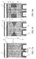
- variable resistances Ra(x) are realised in the connection layer 20 by introducing islands 10 with different resistivity with respect to the remaining conductive area. These islands can have different shapes as shown, only by way of example, in the series of figures 17, 18 and 19 .
- the determinant characteristic is that one or more geometric parameters can vary according to the distance x influencing, in a known way, the resistive contribution Ra(x).
- figure 15 shows a layout of a power MOS device 1 comprising a gate pad 30 connected to two vertical arms 13 with resistance R1 and R2, two external gate fingers 11 and an inner one whose incremental resistances are indicated as R b .
- the total value of the resistances, R b depends on the distance x from a reference which can be the gate pad 30 or an edge to which respect the gate pad 30 is realised.
- the reference is the left edge of the plate whereon the power MOS device 1 is realised.
- connection layer 20 varies when the distance x varies.
- Ra(x) indicates the resistances introduced into the connection layers 20 with the suitable islands 10 formed therein which allow to compensate the different resistance of the gate finger 11 according to the distance x from the left edge of the plate.
- the value of the resistance Ra(x) is chosen so as to exactly compensate the highest value of the resistive contribution of the gate finger 11, as schematised in the diagram reported in figure 16 .
- R b x is the product between the unitary resistance of the conductive layer forming the gate finger and the distance x from the reference side and it represents the resistive value introduces by the gate finger to that position.
- the resistance value Ra equal to the value of resistance Ra(x) which can be calculated with the above indicated formula according to the distance x, must be realised in series to one or to more conductive strips 8 in correspondence with the connection layer 20.
- the resistance Ra can be realised in the connection layer 20 which connects two strips 8 to the gate finger 11, by means of the formation of two independent islands 10, realised transversally to the connection layer 20 and placed at a distance D.
- the value of Ra can be obtained according to the example indicated in figure 19a .
- the islands 10 formed on the upper surface of the connection layer 20 are partially connected to each other to form a structure 21 which exhibits a substantially H-like conformation in plan comprising a central portion 22 and two transversal portions 23.
- the leading idea is that of introducing in the area 20 a resistance whose value varies inside the device so as to compensate the resistive contribution, or better, being dynamic stresses, the impedance introduced by the gate fingers.
- These resistances inside the area 20 can be realised by suitably modifying the shape and/or the number of the islands 10 of conductive material.
- the power MOS device 1, according to the present invention thus allows to realise a gate structure 12, comprising conductive strips 8 and possible structures 20 for connection to the gate fingers 11, with variable resistivity according to the islands 10 being formed which allow to suitably modify the gate global resistivity.
- a further advantage of the present invention is due to the fact that having the gate structure 12 a regulable resistivity, according to the dimensions and the material of the islands 10 formed, it is important to ensure a uniform resistance to each elementary MOS transistor 2 and this allows to uniform the time constant RC of the power MOS device 1 thus ensuring a controlled switch also at high operation frequencies.
- the power MOS device realised by means of the present invention, with a gate structure having programmable resistivity allows to improve and to balance the dynamic response to the signals coming from the gate pad.
Description
- The present invention relates to a power electronic device, such as a MOS device of the type comprising a very high integration of elementary MOS transistors and used in multiple applications both at low and high supply voltage.
- The invention particularly, relates to a power MOS device and the following description is made with reference to this field of application by way of illustration only.
- As it is well known, in power electronic devices, in particular in power devices of the MOS type, it is important to have the possibility of operating at higher and higher frequencies maintaining the component reliability high.
- The nowadays uses of MOS devices in fact require the possibility of operating, both at low supply voltage (20-100V) and at high supply voltage (200-1000V), but, however, at higher and higher frequencies next to the megahertz (MHz).
- Power devices are thus subjected to very high voltage and current gradients during the transients and/or during the switch steps which make the stresses to the device weakening the same burdensome and reduce its activity period in a drastic way.
- As it is well known some power MOS devices are realised by thousands or millions of elementary MOS transistors placed in parallel and individually contributing to the overall capacity in current of the device.
- Typically, elementary MOS transistors, as highlighted in
figure 1 , are realised on semiconductor or with polygonal cells or strips and they comprise a body region, which, in the case shown, is of the p type, formed on a suitable substrate, of the n type, and with a source region realised on top. - The body region, together with the source region, forms a channel region covered by an insulating layer, for example a silicon oxide, and by a conductive layer, for example suitably doped polysilicon.
- These two insulating and conductive layers represent, for each elementary MOS transistor, the gate dielectric and for the power MOS device they form a biasing mesh also called gate mesh.
- The gate mesh is connected to a terminal called gate pad and it allows to distribute the signals inside the MOS device as well as to turn on and/or off all the elementary MOS transistors composing the power MOS device.
- The gate mesh, due to the high polysilicon resistivity (> 10 Ohm/square), exhibits resistive contributions along the path which depend on the relative position with respect to the gate pad, as highlighted in the circuit of
figure 2 , this implies that gate resistance value of each elementary transistor also depends on the distance from the gate pad. - Thus, at each switch of the MOS device, each elementary MOS transistor responds with a time constant which will be distinct, being, as known, a function of the input capacity and of the gate resistance.
- The gate resistance is thus an important value because, together with the input capacity of the MOS device, forms an RC circuit whose time constant is one of the most important parameters influencing the switch speed of power MOS devices. These latter, having to operate at higher and higher frequencies, require a more and more reduced time constant. There is then an attempt to reduce the gate resistance and to make it homogeneous for the entire MOS device so as to ensure a good reliability even at high frequency.
- To try and solve such problem a known technique is that of carrying out a suitable metallisation of the gate, process consisting in creating connection buses also called gate fingers, realised in metallic material, so as to connect the gate pad to various points of the gate mesh by "short-circuiting" them, as shown in
figure 3 and in the corresponding circuit offigure 4 . - A technique is that of increasing the number of gate fingers so as to intersect the gate mesh in the greatest number of points as possible.
- Although advantageous under several aspects, such solution exhibits different drawbacks, the main one is linked to the presence of the gate fingers realised in metallic material which reduce the active area of the power MOS device since below the same it is not possible to integrate the elementary MOS transistors.
- Moreover, a further drawback linked to the presence of the gate fingers is due to the fact that they limit the number and the position of the wires connecting to the source pad thus negatively affecting the output resistance of the power MOS device.
- A further known solution to reduce the gate resistance provides the decrease of the gate mesh resistance by integrating there inside a very conductive layer. Such process makes use of metallic silicides, such as for example cobalt silicide (CoSi2), platinum silicide (PtSi), titanium silicide (TiSi2) or tungsten silicide (WSi2), all materials exhibiting a layer resistivity of about a lower magnitude order with respect to that of the polysilicon.
- For power MOS devices used in faster and faster applications with low gate resistance, problems however emerge linked to the great voltage and current gradients during the transients.
-
Figure 5 highlights a pattern in parallel of a pair of elementary MOS transistors which exhibit different gate resistances according to the position wherein they are with respect to the gate pad and to the gate fingers. - The diagram reported in
figure 6 shows how between elementary MOS transistors wherein there exists an unbalance in the resistance value, during the switch step of the MOS device, different wave forms are produced which distribute the current at stake in a non uniform way. In particular it can be verified how thecurrent intensity 12 crossing the slowest component, undergoes sudden increases negatively affecting the uniformity of the time constant of the MOS device. - Such behaviour in the power MOS device is exponentially increased for the plurality of elementary MOS transistors, this however jeopardises both the correct functionality and the operating duration of the MOS device itself.
- For the manufacturing process used in the realisation of a power MOS device of the known type it is inevitable that there are unbalances in the current progress. In fact it is good to remember that the distance between one gate finger and the other is around values of 200-2000 µm and in such space a lot of elementary MOS transistors are comprised whose gate biasing occurs by means of the gate mesh. In such case the elementary MOS transistors being closer to the gate fingers will be the fastest while the others will be slower and slower, as highlighted in
figure 7 . - Further unbalances are due to the fact that for problems due to the assembling step it is complex to realise continuous and equidistant gate fingers. Thus, the power MOS device obtained will exhibit areas with different distances between the gate fingers, as shown in the example of
figure 8 , and this implies the presence of a gate resistance influenced by the area with shortest distance between the gate fingers, since in the calculation of the parallel the areas with higher resistance will have less weight. - Moreover it is good to reveal that although the resistivity of the material used for realising the gate fingers is low, it is possible that their length is such as to introduce resistive contributions which can be compared with the total gate resistance of the power MOS device especially if, for lowering the metallisation mesh resistance, metallic silicides are used.
- As highlighted in the example of
figure 9 and in the associated circuit offigure 10 , the areas in correspondence with the points A and B although being near the gate finger exhibit a different resistance in series due to the contribution of the gate finger section AB, which could have an even higher weight than one Ohm, with a consequent unbalance between the different areas of the power MOS device. - Considering for example a width of the metallic tracks of the gate finger equal to 10-50 µm, a thickness of the metallic layer between 2-10 µm and fixing at 5mm the width of an aluminium track the values of the minimum resistance of the gate finger will be equal to 0,3 Ohm and the highest equal to 7 Ohm.
- It is good to remember that, in a fast power MOS device there is the need of having a total gate resistance equal to 1 Ohm and then the importance is understood of reducing or voiding the resistive contributions of the gate fingers.
- All these causes lead to have power MOS devices weakened by the presence of areas having different gate resistance with consequent negative effects on the switches and during the extreme dynamic stresses during which there are high values of dV/dt and/or dI/dt.
- The unbalance can also cause current focalisations which can cause the non correct operation and/or the breaking of the power MOS device.
- The article included in the Journal of Vacuum Science & Technology B6(1988)Nov./Dec., No.6, New York, US, pages 1740-1745 (Shenai et al.) discloses a power MOSFET structure fabricated with selectively silicided gate and source regions.
- The technical problem underlying the present invention is that of devising a power MOS device with a high integration density, comprising a plurality of elementary MOS transistors and with such a gate structure as to ensure a uniform resistance and thus a controlled switch and a simultaneous time constant, exhibiting in the meantime such structural and functional characteristics as to allow to overcome the drawbacks cited with reference to the prior art.
- Another aim of the invention is that of uniforming the gate resistance seen from each elementary MOS as much as possible.
- The solution idea underlying the present invention is that of realising a power MOS device comprising a plurality of elementary MOS transistors and a gate structure realised with a conductive material with programmable resistivity exhibiting a plurality of independent islands, suitably distributed and localised.
- On the basis of such solution idea the technical problem is solved by a power MOS device according to
claim 1. Specific embodiments are set out in the dependent claims. - The characteristics and the advantages of the power MOS device according to the invention will be apparent from the following description of embodiments given by way of indicative and non limiting example making reference to the annexed drawings.
-
-
figures 1 and 2 schematically show a section, in an intermediate step of the manufacturing process, of a portion of a power MOS device realised according to the prior art and a corresponding equivalent electric circuit wherein the gate resistance due to the signal distribution by means of the polysilicon mesh (polysilicon gate mesh) is highlighted; -
figure 3 shows, schematically and according to a flat view, the characteristic elements (gate pad, gate fingers, elementary MOS, etc.) of a power MOS device; -
figure 4 shows the equivalent electric scheme of a gate mesh which departs from the gate pad to reach all the elementary MOS; -
figures 5 and 6 show an electric circuit and a diagram reporting the wave forms in voltage and current of a turn off of two elementary MOS transistors of a power MOS device realised according to the prior art; -
figures 7 and 8 show a schematic layout of two different examples of a MOS device according to the prior art; -
figures 9, 9b and 10 schematically show a further example of a power MOS device according to the prior art with the corresponding equivalent circuit; -
figures 11 and 11b show a portion of a power MOS device realised according to the present invention; -
figure 12 shows an equivalent circuit of a portion of a gate structure reported infigure 11 ; -
figures 13 and 14 show a portion of a further embodiment of a power MOS device according to the present invention; -
figure 15 is a schematic view of an embodiment of the device according to the invention wherein the innovations brought according to the present invention with respect to the known solution offigure 9 are highlighted; -
figures 15a and 15c show an equivalent electric scheme in detail (FIG. 15a ) and in blocks (fig. 15c ) of a gate mesh of the device reported infigure 15 ; -
figure 15b shows, only by way of example, how it is possible to realise connection layers with variable resistance according to the present invention; -
figure 16 shows a diagram reporting the progress of a resistance of a gate finger as a function of the length and the progress of a compensation resistance; - the series of
figures 17 to 19a show some embodiments of a layout portion of a MOS device according to the present invention; -
figure 20 proposes again the MOS device offigure 8 wherein some characteristic lengths have been highlighted; -
figure 21 reports a simplified electric scheme of a series of elementary MOS present in the device offigure 20 wherein the value of the resistance in series on the gate is made change according to what has been said in the present invention. - With reference to such figures, and in particular to the embodiment of
figure 11 ,1 globally and schematically indicates a portion of power MOS device realised according to the present invention. - The
device 1 comprises a plurality of elementary MOS transistors 2, arranged in parallel to each other, realised on a silicon plate comprising a semiconductor layer 4 overlapped onto a substrate 3. The layer 4 exhibits a first type of conductivity which, in the case highlighted in the figure, is of the N- type while the substrate 3 is of the N+ type with increased doping. - The elementary MOS transistors 2 shown in the figures are realised only by way of indication with strip-like structures, even if the present invention can be applied on devices with elementary MOS transistors with cellular structure.
- The elementary MOS transistors 2 exhibit a
body region 5, realised with a second type of conductivity, asource region 6 contained abovesuch body region 5 and anoverlying gate oxide 7 which partially covers thebody 5 and thesource region 6 to define an underlying channel region 7a. - The
MOS device 1 exhibits agate structure 12 comprising a plurality ofstrips 8 realised with a first conductive material, such as for example polysilicon, arranged above thegate oxide 7 and self-aligned thereto. - The
strips 8, according to a standard layout, can be directly connected to agate pad 30, suitably provided on the upper surface of theMOS device 1, or they can be connected thereto by means of a plurality of gate fingers ormetallic tracks 11. - The
gate fingers 11, where present, are realised in particularly conductive material, such as a metal, and they thus allow to quickly transfer each signal coming from thegate pad 30 directly to the plurality ofconductive strips 8 and thus to the single elementary MOS transistors 2 electrically connected. - In the example reported in
figure 9 thegate fingers 11 are three, a central one and two lateral ones and, as well highlighted in the otherfigure 9B , between thegate fingers 11 and theconductive strips 8 there is aconnection layer 20 also preferably realised with a conductive material, such as for example polysilicon. This connectionconductive layer 20 introduces a further resistive contribution (Ra) in series to the conductive strips 8 (fig. 10 ) whose value depends on the number and on the dimensions of theislands 10. - The
gate structure 12 has programmable resistivity and it comprises a plurality ofislands 10 realised with at least a second conductive material having a different resistivity than that of the first conductive material. The plurality ofislands 10 are formed on anupper surface 9 of saidconductive strips 8. - Suitably, the plurality of
islands 10 is realised for example with a metallic silicide or by means of ionic implantation of doping species. In the most advantageous case these islands can be realised by means of selective silicidation of the polysilicon. - A further realisation could however provide that a group of
islands 10, or eachisland 10 of said plurality, can be realised with a conductive material different from another group or from anotherisland 10. - Each
island 10 exhibits, in plan, a polygonal conformation. In the preferred embodiment shown infigure 11 eachisland 10 has a rectangular conformation. - Preferably, the plurality of
islands 10 formed on theupper surface 9 of thestrip 8 are aligned along suchconductive strip 8 and they exhibit realisation parameters of length Co, of width X and of distance p from the preceding which, although varying, meet some relations as better specified hereafter. The depth of theseislands 10 depends on the formation process and it is a fix parameter inside the device. - The plurality of
islands 10 formed on theupper surface 9 allow to create resistances of suitable value to be connected in series and/or in parallel to theconductive strips 8 to compensate their resistive values. - Each
island 10 formed on theupper surface 9 of thestrip 8 projects therefrom, as shown in the section offigure 11b and it leans on a polysilicon layer. - According to different embodiments each
island 10 can be completely contained in the polysilicon layer or wrapped by the polysilicon layer of theconductive strip 8 with an upper surface coplanar with thesurface 9 of thestrip 8 or realised on thesurface 9 of thestrip 8. - Naturally, the values of such realisation parameters of the
islands 10 will have to be compatible with the technology used and the equipments employed. Moreover, the conductive material with which theislands 10 can be realised can vary according to the specific needs, being for example cobalt silicide (CoSi2), platinum silicide (PtSi), titanium silicide (TiSi2) or tungsten silicide (WSi2). - As already said, moreover, the
islands 10 can be realised also by means of selective ionic implantation of doping species which change the resistivity of thepolysilicon layer 8 inside theisland 10. - The determinant fact for the invention is that the
islands 10 have a different resistivity with respect to the remainingparts 15 of theconductive strip 8. - Thus, the
conductive strip 8 with programmable resistivity will havefirst portions 15 realised in a polysilicon layer alternative withsecond portions 16 realised by a polysilicon layer and with a silicide layer which defines theisland 10. - From the electric point of view the resistance of a
conductive strip 8, according to the present invention, has an equivalent circuit reported infigure 12 and it is considered as a series n, where n is the number of islands (10) suitably formed in said conductive strip (8), of polysylicon resistances Rpoly 1,2,..n of thefirst portions 15 alternated with polysilicon resistances Rpoly 1a,2a,...na in parallel with silicide resistances Rsil 1,2,...n of thesecond portions 16. - In particular, with reference to
figure 11 , the unitary resistance r of astrip element 8 havinglength 1, realised by afirst portion 15 and by asecond portion 16 being contiguous, will be given by the formula:
wherein: - s is the width of the
conductive strip 8 and x is the width of eachisland 10;
it results:
- rp the unitary resistance associated with the
first portion 15 in the section p of theconductive strip 8, i.e. rp=Rsp/s where Rsp is the layer resistance (sheet resistance) of thefirst portion 15; - rco the unitary resistance associated with the
second portion 16, section Co of theconductive strip 8, i.e. the parallel between the layer resistance of the polysilicon in the section (s-x) and of silicide+silicon in the section. - As it is well known, the resistance value of each
conductive strip 8 influences the time constant of the elementary MOS transistors 2 electrically connected to thestrip 8 and in particular the response of theMOS device 1 to each signal coming from thegate pad 30 is influenced. - Advantageously the values of the realisation parameters of the
islands 10 will be predefined so that eachconductive strip 8 responds to each signal coming from thegate pad 30 with a same time constant. - With a simplified analysis it results that the time constant of a
conductive strip 8 of length L is equal to (rL)*(cL) where r and c are respectively unitary resistance and capacity of thestrip 8. - Naturally, the unitary capacity c depends on the width s of the
conductive strip 8 and on the thickness of theunderlying gate oxide 7 and it is thus a constant according to the technologies used, in particular it will be independent from theislands 10 introduced. - Thus, indicating with Lmax the length of a
longer strip 8, schematically shown in the examples offigures 20 and 21 , and with L the one of ashorter strip 8 and wishing to uniform the time constant RC a relation between the various parameters is attained. - In such case, wishing to speed up the
longest strip 8 theislands 10 formed will realise a continuous strip with maximum width and thus with a unitary resistance which will be equal to: r= r(Lmax) = rco. Thus, imposing the equality between the time constants the following relation is obtained:
- Such relation links the realisation parameters of the plurality of
islands 10 to the ratio between the lengths of the smallest and greatestconductive strips 8. - By using realisation parameter, being variable but meeting the above indicated relation, the time constant of the
MOS device 1 can be corrected to ratios meeting the following relation:
- In such case according to the geometries typical of the technology used as well as to the resolution of the type of photolitographic equipments used (Lmax/L) values are attained being equal to about 3-5, values which allow to obtain a good definition of the time constant and thus of the response of the
power MOS device 1 to the external stresses. - Naturally, as above highlighted, the
islands 10 can have correlated realisation parameters and variable arrangements. In particular, according to a second embodiment, as highlighted infigure 13 , theislands 10 can be contiguous with at least one attached side, thus forming acontinuous strip 25 along theconductive strip 8. - According to such embodiment, the variable dimensional parameter of each
island 10 is the width X of thecontinuous strip 25. - In particular, wishing to uniform all the time constants of the
conductive strips 8, which realise thegate structure 12 of thepower MOS device 1, and the time constants being, as known, a function of RC, where R is the resistance and C the capacity, it is possible to vary the width of thecontinuous strip 25, for example by increasing the width X for making theshortest strips 8 become slower. - In the simplified embodiment highlighted in
figure 13 , the unitary resistance r is given by the parallel between: - the resistance of a polysilicon unitary portion, given by the ratio:

- Carrying out thus the calculation of the parallel the value of the unitary resistance is equal to:

wherein Lmax is the maximum length of theconductive strips 8 and xmax is the greatest width of thecontinuous strip 25 formed therein, this latter value depending on the technologies used, and imposing the equality of the time constants with anystrip 8 of parameters: L of length and x of width of thecontinuous strip 25, the following relation will result:
wherein - Rsp, is a resistance of the
strip portion 8 of the polysilicon layer with thickness a, will have values of about 30-45 Ohm/[], - Rspsi is a resistance of the
strip portion 8 realised by the parallel of the polysilicon layer with reduced thickness b and of the overlapped silicide layer of thecontinuous strip 25, will have values of about 0.5-5 Ohm/[] - s is the width of the
conductive strip 8. - Such solutions allow to solve, or however to attenuate, the unevenness effect of the gate resistance of the single elementary MOS due to the different length of the conductive strips 8 (see the case reported in
figure 8 ). - From the electric point of view, the
power MOS device 1 in the case shown infigure 9 exhibits the threegate fingers 11 which, being realised as metallic tracks, add resistances (Rb infig. 10 ) in series to the resistances of theconductive strips 8 which can, separately according to their dimensions, introduce, according to prior art, resistance values equal to 0,3-7 Ohm. - Since it is not possible to void such resistive contribution, a second aim of the present invention is that of compensating the effect of this contribution of each
gate finger 11 so as to uniform the resistive contribution seen from all the series of elementary MOS (strip 8) connected thereto. - According to the present invention, for reducing the unevenness of the gate resistance generated due to the resistances introduced by the
gate fingers 11, between eachgate finger 11 and one or moreconductive strips 8, resistances (Ra(x)) are realised whose value depends on the distance x from the gate pad or from the start of the gate finger (fig. 15a). Figure 15c reports a block equivalent electric scheme of the device offigure 15 wherein the resistances of the gate fingers (Rb) and the additional ones of theconnection layer 20 are highlighted whose value depends on the position. - Such resistances, also called balance resistances and realised in the
connection layer 20, allow to compensate the different resistive contribution of thegate fingers 11 according to the distance x from thegate pad 30. - The variable resistances Ra(x) are realised in the
connection layer 20 by introducingislands 10 with different resistivity with respect to the remaining conductive area. These islands can have different shapes as shown, only by way of example, in the series offigures 17, 18 and19 . - The determinant characteristic is that one or more geometric parameters can vary according to the distance x influencing, in a known way, the resistive contribution Ra(x).
- For example,
figure 15 shows a layout of apower MOS device 1 comprising agate pad 30 connected to twovertical arms 13 with resistance R1 and R2, twoexternal gate fingers 11 and an inner one whose incremental resistances are indicated as Rb. - Naturally, the total value of the resistances, Rb, depends on the distance x from a reference which can be the
gate pad 30 or an edge to which respect thegate pad 30 is realised. In the case shown infigure 15 the reference is the left edge of the plate whereon thepower MOS device 1 is realised. - An example of how the structure of the
connection layer 20 varies when the distance x varies is reported infigure 15b . - In such representation (
fig. 15a ) Ra(x) indicates the resistances introduced into the connection layers 20 with thesuitable islands 10 formed therein which allow to compensate the different resistance of thegate finger 11 according to the distance x from the left edge of the plate. - Advantageously according to the present invention the value of the resistance Ra(x) is chosen so as to exactly compensate the highest value of the resistive contribution of the
gate finger 11, as schematised in the diagram reported infigure 16 . - In such way the value of the series between the resistance Ra(x) and the resistance introduced by the gate finger to that position x will have to be constant and equal to the highest resistance. Thus the value of Ra(x), although depending on the distance x from the reference, will be highest for x=0 and minimum for x=xmax.
- Then, for carrying out the compensation of the resistive value of the gate finger Rb it is necessary to single out the farthest point in resistive terms from the
gate pad 30, so as to fix the highest resistance value (Rmax) to be compensated. - It is thus possible to calculate Ra(x) imposing that the value of the resistance to be compensated, due to the
gate finger 11, both equal to Rmax, i.e. that:
wherein: - R(x=0) is the resistance in series on the branch coming from the gate pad considered for x=0 (for example for the edge R(x=0)= R1 + R2, while for the central gate finger 11 (R(x=0)= R1).
- Rb x is the product between the unitary resistance of the conductive layer forming the gate finger and the distance x from the reference side and it represents the resistive value introduces by the gate finger to that position.
- Thus, making explicit with respect to Ra(x) the relation is obtained:

- Naturally, the resistance value Ra, equal to the value of resistance Ra(x) which can be calculated with the above indicated formula according to the distance x, must be realised in series to one or to more
conductive strips 8 in correspondence with theconnection layer 20. - In a preferred embodiment indicated in
figure 18a , the resistance Ra can be realised in theconnection layer 20 which connects twostrips 8 to thegate finger 11, by means of the formation of twoindependent islands 10, realised transversally to theconnection layer 20 and placed at a distance D. -
Such connection layer 20, with the twoislands 10, exhibits an additional resistance Ra of value equal to:
wherein:
- La is the width of theconnection layer 20 and in such case also of theislands 10;
D is the distance between the two islands and Rsp the resistance of theconnection layer 20 realised only in polysilicon;
Rspsi is the resistance of theconnection layer 20 realised as overlapping between the polysilicon layer and the islands (10) realised with silicide. - According to a further embodiment the value of Ra can be obtained according to the example indicated in
figure 19a . - Advantageously, the
islands 10 formed on the upper surface of theconnection layer 20, are partially connected to each other to form astructure 21 which exhibits a substantially H-like conformation in plan comprising acentral portion 22 and twotransversal portions 23. - Indicating with
- h the height and b the width of the central portion of the
structure 21; - La the width of the connection layer;
- Rsp the resistance of the parts of
connection layer 20 realised only in polysilicon, which, according to the present embodiment, are twoparts 24 lateral to thecentral portion 21; - Rspsi the resistance of the
connection layer 20 with thestructure 21 realised with silicide overlapped; - Thus, advantageously by predefining the values of height h, width b of the
structure 21 ofislands 10, and La width of theconnection layer 20 suitable additional resistances Ra of predetermined value can be realised. - The shapes taken by the
islands 10 and the cutting or narrowing positions can be obviously different according to the design needs.Figures 17 to 19 show in fact only an example. - The leading idea is that of introducing in the area 20 a resistance whose value varies inside the device so as to compensate the resistive contribution, or better, being dynamic stresses, the impedance introduced by the gate fingers.
- These resistances inside the
area 20 can be realised by suitably modifying the shape and/or the number of theislands 10 of conductive material. - The
power MOS device 1, according to the present invention, thus allows to realise agate structure 12, comprisingconductive strips 8 andpossible structures 20 for connection to thegate fingers 11, with variable resistivity according to theislands 10 being formed which allow to suitably modify the gate global resistivity. - The dimensional parameters with which the
islands 10 are realised are correlated with the elementary MOS positions inside the device, and the above indicated relations represent only an example. - In particular
plural islands 10 will be introduced whose resistances will be in series or in parallel to the resistances of theconductive strips 8 allowing to improve the time constant of eachconductive strip 8 and uniforming the response of thepower MOS device 1 to each signal coming from thegate pad 30. - An improvement will be thus obtained of the dynamic operation of the power MOS device which will result to be programmable on the basis of the dimensional values of the islands inserted.
- A further advantage of the present invention is due to the fact that having the gate structure 12 a regulable resistivity, according to the dimensions and the material of the
islands 10 formed, it is important to ensure a uniform resistance to each elementary MOS transistor 2 and this allows to uniform the time constant RC of thepower MOS device 1 thus ensuring a controlled switch also at high operation frequencies. - More in particular, the power MOS device realised by means of the present invention, with a gate structure having programmable resistivity allows to improve and to balance the dynamic response to the signals coming from the gate pad.
and of the unitary resistance of the

wherein Rspsi is the resistance of the polysilicon layer with reduced thickness b and the overlapped silicide layer, while x is the width of the

Claims (17)
- Power MOS device of the type comprising- a plurality of elementary power MOS transistors (2) having a body region (5) and a source region (6) above said body region (5); and- a gate structure (12) comprising a plurality of strips (8) realised with a first conductive material;wherein said gate structure (12) comprises a plurality of islands (10) realised with at least one second conductive material having a different resistivity than that of the first conductive material and projecting in said plurality of conductive strips (8), each of said conductive strips (8) comprises n of said islands (10) and exhibits an equivalent electric circuit formed by a series of first resistive elements, associated with said first conductive material with which said strips (8) are formed, and second resistive elements, each formed by a second resistance associated with said first conductive material in correspondence with the islands (10) in parallel with a third resistance associated with said second conductive material with which the islands (10) are realised, said first and second resistive elements being alternated with each other in said series,
and wherein said series of resistances vary from point to point inside the device. - Device according to claim 1 wherein said islands (10) exhibit, in plan, a polygonal conformation.
- Device according to claim 1 wherein said islands (10) exhibit, in plan, a rectangular conformation.
- Device according to claim 2 wherein said plurality of islands (10) are aligned along said strip (8).
- Device according to any one of the preceding claims wherein said islands (10) are contiguous with at least one side attached.
- Device according to claim 4 wherein said islands (10) with said at least one side attached form a continuous strip (25) along said conductive strip (8).
- Device according to claim 2 wherein each island (10) formed on said upper surface (9) realised with said second conductive material comprises realisation parameters of length Co, of width X and of distance p from the preceding island (10) which allow to create a resistance Rsi to be connected in series and/or in parallel to resistances Rsp created by said conductive strips (8).
- Device according to claim 1 wherein said conductive strips (8) are realised in polysilicon and have first portions (15) realised with a single polysilicon layer alternated with second portions (16) realised with a polysilicon layer overlapped with said island (10) formed with a silicide layer.
- Device according to claim 7 wherein said realisation parameters of each island (10) of said plurality of islands (10) are in relation to the values of the lengths of said strips (8).
- Device according to claim 7 wherein said realisation parameters of each island (10) of said plurality of islands (10) are in relation to the values of the lengths of said conductive strips (8) according to the following relation:

where 1 is said length of said element sum between said length p of said first portion (15) and said length Co of said second portion (16), rp said unitary resistance of said first portion (15) and rCo said unitary resistance of said second portion (16), L a length of said conductive strips (8) and Lmax a maximum length of said conductive strips (8). - Device according to claim 6 wherein said continuous strips (25) of islands (10) formed along said conductive strips (8) exhibit a dimensional width X in relation to the length L of said strips (8).
- Device according to claim 6 wherein indicating with Lmax a maximum length of said strips (8) and xmax a maximum width of said continuous strip (25) formed in said maximum strip (8), and L indicating the length of one of said conductive strips (8), a width of a continuous strip (25) formed on said strip (8) of length L meets the following relation:

whereinRsp is said resistance of said polysilicon portion;Rspsi is said polysilicon resistance comprising said continuous strip (25);s is a width of said conductive strip (8). - Device according to claim 12 wherein said resistance Rsp has values comprised between 30 and 45 Ohm/□ and in that said resistance Rspsi has values comprised between 0.5 and 5 Ohm/□.
- Device according to any one of the preceding claims comprising a gate pad (30) and one or more gate fingers (11) suitable to transmit signals from said gate pad (30) to said conductive strips (8) by means of a connection with a connection layer (20) realised with polysilicon wherein said connection layer (20) comprises at least one island (10) realised with a second conductive material.
- Device according to claim 14 wherein being Rmax a maximum resistance of said gate fingers (11) and being Ra(x) an additional resistance of said connection layer (20) comprising one or more of said islands (10) said additional resistance Ra(x) meets the following relation:

wherein:R(x=0) is a resistance in series to each of said gate fingers (11) according to the distance from said gate pad (30);Rbx is the resistance introduced by said gate finger (11) to a distance x; - Device according to claim 15 wherein said islands (10) realised in said connection layer (20) are two realised transversally and spaced by a distance D and in that said additional resistance Ra(x) is given by:

wherein:- L is a width and H a total length of said connection layer (20)- D is said distance between said two islands (10);- Rsp is a resistance of said connection layer (20) realised by a layer with only polysilicon;- Rspsi is a resistance of said connection layer (20) realised by said polysilicon layer overlapped with said islands (10). - Device according to claim 15 wherein said islands (10) realised in said connection layer (20) are partially connected to each other to form a structure (21) exhibiting a substantially H-like conformation in plan comprising a central portion (22) and two transversal portions (23), and in that said additional resistance Ra(x) is equal to:

wherein:- L is a width of said connection layer (20);- h and b are the height and width of said central portion (22) of said structure (21) realised in a polysilicon layer and a silicide layer being overlapped exhibiting a resistance equal to Rspsi;- Rsp is a resistance of said connection layer (20) realised in a single polysilicon layer.
Applications Claiming Priority (1)
| Application Number | Priority Date | Filing Date | Title |
|---|---|---|---|
| IT002245A ITMI20042245A1 (en) | 2004-11-19 | 2004-11-19 | MOS POWER ELECTRONIC DEVICE WITH CONTROLLED SWITCHING |
Publications (2)
| Publication Number | Publication Date |
|---|---|
| EP1659636A1 EP1659636A1 (en) | 2006-05-24 |
| EP1659636B1 true EP1659636B1 (en) | 2009-11-04 |
Family
ID=35589628
Family Applications (1)
| Application Number | Title | Priority Date | Filing Date |
|---|---|---|---|
| EP05025285A Expired - Fee Related EP1659636B1 (en) | 2004-11-19 | 2005-11-18 | Power MOS semiconductor device |
Country Status (3)
| Country | Link |
|---|---|
| EP (1) | EP1659636B1 (en) |
| DE (1) | DE602005017457D1 (en) |
| IT (1) | ITMI20042245A1 (en) |
Families Citing this family (2)
| Publication number | Priority date | Publication date | Assignee | Title |
|---|---|---|---|---|
| US8664713B2 (en) | 2008-12-31 | 2014-03-04 | Stmicroelectronics S.R.L. | Integrated power device on a semiconductor substrate having an improved trench gate structure |
| JP2024009766A (en) | 2022-07-11 | 2024-01-23 | エスティーマイクロエレクトロニクス エス.アール.エル. | Power mosfet device with improved isolated gate structure and manufacturing process thereof |
-
2004
- 2004-11-19 IT IT002245A patent/ITMI20042245A1/en unknown
-
2005
- 2005-11-18 DE DE602005017457T patent/DE602005017457D1/en active Active
- 2005-11-18 EP EP05025285A patent/EP1659636B1/en not_active Expired - Fee Related
Also Published As
| Publication number | Publication date |
|---|---|
| EP1659636A1 (en) | 2006-05-24 |
| DE602005017457D1 (en) | 2009-12-17 |
| ITMI20042245A1 (en) | 2005-02-19 |
Similar Documents
| Publication | Publication Date | Title |
|---|---|---|
| US7569883B2 (en) | Switching-controlled power MOS electronic device | |
| CN110945662B (en) | Integrated gate resistor for semiconductor power conversion device | |
| US6933563B2 (en) | High performance, integrated, MOS-type semiconductor device and related manufacturing process | |
| KR20090036831A (en) | Wiring structure in semiconductor device and method of forming the same | |
| US5801091A (en) | Method for current ballasting and busing over active device area using a multi-level conductor process | |
| EP1659636B1 (en) | Power MOS semiconductor device | |
| JP3677346B2 (en) | Semiconductor devices that can be controlled by field effects | |
| EP0544364B1 (en) | Monolithic semi-conductor device having a vertical structure with a deep-base and finger-emitter power transistor having a ballast resistance | |
| US6140680A (en) | Integrated power semiconductor transistor with current sensing | |
| US5977587A (en) | Semiconductor device and a method for wiring of a semiconductor device | |
| EP0731985A1 (en) | Improved mesh geometry for mos-gated semiconductor devices | |
| KR100298819B1 (en) | Structure for esd protection in semiconductor chips | |
| EP0330299A2 (en) | Semi-custom integrated circuit | |
| US7205880B2 (en) | Trimmer impedance component, semiconductor device and trimming method | |
| EP1618607B1 (en) | Semiconductor device comprising an ldmos field-effect transistor and method of operating the same | |
| WO2007146899A2 (en) | Rf power transistor device with high performance shunt capacitor and method thereof | |
| US7105912B2 (en) | Resistor structure and method for manufacturing the same | |
| EP1659638B1 (en) | Power MOS device and corresponding manufacturing method | |
| DE102018108561B3 (en) | TRANSISTOR COMPONENT WITH GATE RESISTANCE | |
| US20100289087A1 (en) | Semiconductor device and method of manufacturing a semiconductor device | |
| JPH0846198A (en) | Semiconductor device | |
| US7923751B2 (en) | Bipolar transistor with a low saturation voltage | |
| EP1296380B1 (en) | Variable capacitance capacitor | |
| US20040067610A1 (en) | RF semiconductor devices and methods for fabricating the same | |
| JP6800026B2 (en) | Semiconductor devices and methods for manufacturing semiconductor devices |
Legal Events
| Date | Code | Title | Description |
|---|---|---|---|
| PUAI | Public reference made under article 153(3) epc to a published international application that has entered the european phase |
Free format text: ORIGINAL CODE: 0009012 |
|
| AK | Designated contracting states |
Kind code of ref document: A1 Designated state(s): AT BE BG CH CY CZ DE DK EE ES FI FR GB GR HU IE IS IT LI LT LU LV MC NL PL PT RO SE SI SK TR |
|
| AX | Request for extension of the european patent |
Extension state: AL BA HR MK YU |
|
| 17P | Request for examination filed |
Effective date: 20061113 |
|
| 17Q | First examination report despatched |
Effective date: 20061215 |
|
| AKX | Designation fees paid |
Designated state(s): DE FR GB IT |
|
| GRAP | Despatch of communication of intention to grant a patent |
Free format text: ORIGINAL CODE: EPIDOSNIGR1 |
|
| GRAS | Grant fee paid |
Free format text: ORIGINAL CODE: EPIDOSNIGR3 |
|
| GRAA | (expected) grant |
Free format text: ORIGINAL CODE: 0009210 |
|
| AK | Designated contracting states |
Kind code of ref document: B1 Designated state(s): DE FR GB IT |
|
| REG | Reference to a national code |
Ref country code: GB Ref legal event code: FG4D |
|
| REF | Corresponds to: |
Ref document number: 602005017457 Country of ref document: DE Date of ref document: 20091217 Kind code of ref document: P |
|
| RAP2 | Party data changed (patent owner data changed or rights of a patent transferred) |
Owner name: STMICROELECTRONICS SRL |
|
| PLBE | No opposition filed within time limit |
Free format text: ORIGINAL CODE: 0009261 |
|
| STAA | Information on the status of an ep patent application or granted ep patent |
Free format text: STATUS: NO OPPOSITION FILED WITHIN TIME LIMIT |
|
| 26N | No opposition filed |
Effective date: 20100805 |
|
| GBPC | Gb: european patent ceased through non-payment of renewal fee |
Effective date: 20100204 |
|
| PG25 | Lapsed in a contracting state [announced via postgrant information from national office to epo] |
Ref country code: GB Free format text: LAPSE BECAUSE OF NON-PAYMENT OF DUE FEES Effective date: 20100204 |
|
| PGFP | Annual fee paid to national office [announced via postgrant information from national office to epo] |
Ref country code: IT Payment date: 20101103 Year of fee payment: 6 |
|
| PG25 | Lapsed in a contracting state [announced via postgrant information from national office to epo] |
Ref country code: IT Free format text: LAPSE BECAUSE OF NON-PAYMENT OF DUE FEES Effective date: 20121118 |
|
| PGFP | Annual fee paid to national office [announced via postgrant information from national office to epo] |
Ref country code: FR Payment date: 20131121 Year of fee payment: 9 Ref country code: DE Payment date: 20131022 Year of fee payment: 9 |
|
| REG | Reference to a national code |
Ref country code: DE Ref legal event code: R119 Ref document number: 602005017457 Country of ref document: DE |
|
| REG | Reference to a national code |
Ref country code: FR Ref legal event code: ST Effective date: 20150731 |
|
| PG25 | Lapsed in a contracting state [announced via postgrant information from national office to epo] |
Ref country code: DE Free format text: LAPSE BECAUSE OF NON-PAYMENT OF DUE FEES Effective date: 20150602 |
|
| PG25 | Lapsed in a contracting state [announced via postgrant information from national office to epo] |
Ref country code: FR Free format text: LAPSE BECAUSE OF NON-PAYMENT OF DUE FEES Effective date: 20141201 |