EP1659637A2 - Verfahren zur Herstellung einer MOS-Leistungsanordnung - Google Patents
Verfahren zur Herstellung einer MOS-Leistungsanordnung Download PDFInfo
- Publication number
- EP1659637A2 EP1659637A2 EP05025287A EP05025287A EP1659637A2 EP 1659637 A2 EP1659637 A2 EP 1659637A2 EP 05025287 A EP05025287 A EP 05025287A EP 05025287 A EP05025287 A EP 05025287A EP 1659637 A2 EP1659637 A2 EP 1659637A2
- Authority
- EP
- European Patent Office
- Prior art keywords
- layer
- power mos
- mos device
- dielectric layer
- hard mask
- Prior art date
- Legal status (The legal status is an assumption and is not a legal conclusion. Google has not performed a legal analysis and makes no representation as to the accuracy of the status listed.)
- Granted
Links
Images


Classifications
-
- H—ELECTRICITY
- H10—SEMICONDUCTOR DEVICES; ELECTRIC SOLID-STATE DEVICES NOT OTHERWISE PROVIDED FOR
- H10D—INORGANIC ELECTRIC SEMICONDUCTOR DEVICES
- H10D30/00—Field-effect transistors [FET]
- H10D30/60—Insulated-gate field-effect transistors [IGFET]
- H10D30/64—Double-diffused metal-oxide semiconductor [DMOS] FETs
- H10D30/66—Vertical DMOS [VDMOS] FETs
-
- H—ELECTRICITY
- H10—SEMICONDUCTOR DEVICES; ELECTRIC SOLID-STATE DEVICES NOT OTHERWISE PROVIDED FOR
- H10D—INORGANIC ELECTRIC SEMICONDUCTOR DEVICES
- H10D30/00—Field-effect transistors [FET]
- H10D30/01—Manufacture or treatment
- H10D30/021—Manufacture or treatment of FETs having insulated gates [IGFET]
- H10D30/028—Manufacture or treatment of FETs having insulated gates [IGFET] of double-diffused metal oxide semiconductor [DMOS] FETs
- H10D30/0291—Manufacture or treatment of FETs having insulated gates [IGFET] of double-diffused metal oxide semiconductor [DMOS] FETs of vertical DMOS [VDMOS] FETs
-
- H10D64/0133—
-
- H—ELECTRICITY
- H10—SEMICONDUCTOR DEVICES; ELECTRIC SOLID-STATE DEVICES NOT OTHERWISE PROVIDED FOR
- H10D—INORGANIC ELECTRIC SEMICONDUCTOR DEVICES
- H10D64/00—Electrodes of devices having potential barriers
- H10D64/20—Electrodes characterised by their shapes, relative sizes or dispositions
- H10D64/27—Electrodes not carrying the current to be rectified, amplified, oscillated or switched, e.g. gates
- H10D64/311—Gate electrodes for field-effect devices
- H10D64/411—Gate electrodes for field-effect devices for FETs
- H10D64/511—Gate electrodes for field-effect devices for FETs for IGFETs
- H10D64/517—Gate electrodes for field-effect devices for FETs for IGFETs characterised by the conducting layers
- H10D64/518—Gate electrodes for field-effect devices for FETs for IGFETs characterised by the conducting layers characterised by their lengths or sectional shapes
-
- H—ELECTRICITY
- H10—SEMICONDUCTOR DEVICES; ELECTRIC SOLID-STATE DEVICES NOT OTHERWISE PROVIDED FOR
- H10D—INORGANIC ELECTRIC SEMICONDUCTOR DEVICES
- H10D64/00—Electrodes of devices having potential barriers
- H10D64/20—Electrodes characterised by their shapes, relative sizes or dispositions
- H10D64/27—Electrodes not carrying the current to be rectified, amplified, oscillated or switched, e.g. gates
- H10D64/311—Gate electrodes for field-effect devices
- H10D64/411—Gate electrodes for field-effect devices for FETs
- H10D64/511—Gate electrodes for field-effect devices for FETs for IGFETs
- H10D64/517—Gate electrodes for field-effect devices for FETs for IGFETs characterised by the conducting layers
- H10D64/519—Gate electrodes for field-effect devices for FETs for IGFETs characterised by the conducting layers characterised by their top-view geometrical layouts
-
- H—ELECTRICITY
- H10—SEMICONDUCTOR DEVICES; ELECTRIC SOLID-STATE DEVICES NOT OTHERWISE PROVIDED FOR
- H10D—INORGANIC ELECTRIC SEMICONDUCTOR DEVICES
- H10D64/00—Electrodes of devices having potential barriers
- H10D64/60—Electrodes characterised by their materials
- H10D64/66—Electrodes having a conductor capacitively coupled to a semiconductor by an insulator, e.g. MIS electrodes
- H10D64/661—Electrodes having a conductor capacitively coupled to a semiconductor by an insulator, e.g. MIS electrodes the conductor comprising a layer of silicon contacting the insulator, e.g. polysilicon having vertical doping variation
- H10D64/662—Electrodes having a conductor capacitively coupled to a semiconductor by an insulator, e.g. MIS electrodes the conductor comprising a layer of silicon contacting the insulator, e.g. polysilicon having vertical doping variation the conductor further comprising additional layers, e.g. multiple silicon layers having different crystal structures
- H10D64/663—Electrodes having a conductor capacitively coupled to a semiconductor by an insulator, e.g. MIS electrodes the conductor comprising a layer of silicon contacting the insulator, e.g. polysilicon having vertical doping variation the conductor further comprising additional layers, e.g. multiple silicon layers having different crystal structures the additional layers comprising a silicide layer contacting the layer of silicon, e.g. polycide gates
Definitions
- the present invention relates to a process for the realisation of a high integration density power MOS device.
- the invention relates to a process for the realisation of a high integration density power MOS device comprising the steps of:
- VLSI Very Large-Scale Integration
- the need is added of driving power MOS devices, with lower and lower gate voltages, so as to allow the corresponding driving circuits [driver] a low voltage output (1.8-2.5 Volt).
- the gate dielectric thickness typically silicon oxide
- the gate dielectric thickness is more and more reduced so as to obtain threshold voltage values lower than the Volt without deteriorating the breakdown characteristics of the MOS device due to a possible punch through effect of the channel whose length is more and more reduced.
- the reduction of the gate dielectric thickness, together with the higher integration density implies an increase of the MOS device capacities and thus a slowdown in the switch.
- the switch speed does not exclusively depend on the capacity but also on the resistance seen from the driver for loading and unloading the capacitive elements of the power MOS device.
- Such resistance takes the name of inner gate resistance and it depends on the physical and geometrical characteristics of the group of all the elementary structures.
- Such elementary transistors have a common control terminal Gate and common conduction terminals Drain and Source.
- a first known solution turned towards minimising the capacity, consists in integrating, in MOS technologies, gate dielectrics different from thermal SiO 2 such as for example, hafnium oxide, aluminium oxide, multilayers of silicon oxide/silicon nitride, etc.
- a second known solution turned towards minimising the capacity, by increasing the switch speed of the device, provides a change of the geometry of the single transistor elementary structure of the power MOS device.
- this structure is changed in the gate dielectric in active area, which is realised with two layers having different thickness:
- the definition procedure of the gate electrode mainly requires a thermal growth of a silicon oxide thick film OX, its photolithographic definition in active area regions, the successive growth of a thin gate oxide film OXG which will surmount a channel ch.
- a gate poly electrode doped polysilicon or polysilicon stack / metallic silicide
- the definition of the gate geometries through suitable phototechnique maskings then follow.
- the prior art for the realisation of a gate with double oxide thickness, of a transistor elementary structure of power MOS devices clashes on the growing need of increasing the integration density however safeguarding the alignment of the planar structures in active area.
- the prior art provides the use of a photolithography to define the thick oxide region OX in the transistor elementary structure and of a successive and more delicate photolithography step for the definition of the gate poly electrode geometry.
- a margin indicated with L in figure 2 must be sufficiently wide as to ensure that possible maximum misalignments in the lithographic definition of the gate poly electrode do not determine a channel extension L ch under the thick oxide OX however in an asymmetrical way.
- FIG. 3 shows a structure 3 with double self-aligning gate thickness of power VDMOS devices.
- This structure has two VDMOS devices, indicated with T1 and T2, having a first gate dielectric thickness, indicated respectively with OXG1 and OXG2 and a second gate dielectric thickness, indicated respectively with OX1 and OX2.
- Opposite spacers SP delimit an opening IN, through which the plants for the formation of body wells are realised, from the start of the thick oxide OX1 and OX2.
- a margin L I comprised between the projection B I of an end of the opening IN through which the plants for the formation of body wells are realised and the projection A I of the end of the thick oxide OX1 nearer to the opening IN, is lower than the margin D1 shown in fig.2.
- the technical problem underlying the present invention is that of defining a process for realising a high integration density power MOS device, with gate electrode having double oxide thickness, having such structural characteristics as to be used also in technologies with scale dimensions VLSI, but with channel dimensions being not necessarily submicrometric, overcoming the limits and/or the drawbacks of the embodiments proposed by the prior art.
- the solution idea underlying the present invention is that of realising a high integration density power device with structure having double gate thickness, the structure being totally self-aligned with the gate electrode.
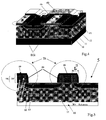
- FIG. 5 an enlarged vertical section view is shown of a high integration density power MOS device, comprising transistor elementary structures, according to a first embodiment of the present invention, is globally and schematically indicated with 5.
- the power device 5 essentially comprises a heavily doped semiconductor substrate of the N type (N+) to ensure the conduction and resistance characteristics in voltage of the desired power device.
- a second doped semiconductor layer of the N type is grown (N-) with lower conductivity with respect to the first layer.
- This layer of greater thickness defines a central portion 17 delimited by polysilicon lateral portions 18.
- a so called conductor polysilicon mesh realises the connection of all the elementary transistors Ti to define the high integration density power MOS device 5, as schematically shown in the prior art description, with reference to figure 1.
- the central portion 17 of thick dielectric is realised with a thermally grown silicon oxide; alternatively, it can be realised with a sequence of suitable layers such as, for example, multilayers of SixOy/SiwNz or SixOyNz.
- the gate structure 14 further comprises an upper nitride portion 19, arranged above the thick dielectric central portion 17 of the transistor mesh and of the polysilicon lateral portions 18; this nitride portion 19 insulates the entire upper base surface of the above portions 17 and 18.
- the gate structure 14, surmounted by the nitride portion 19, is flanked by two spacers 20 of conductive material, arranged so as to cover, with their own base, the opposite ends of the upper surface of the first thin layer 15 of gate oxide, left free since not overlapped neither by the thick dielectric central portion 17 of the transistor mesh nor by the lateral polysilicon portions 18.
- the two spacers 20 of conductive material serve as gate electrode.
- the above spacers 20 are realised with suitably doped polysilicon; alternatively, they can be realised with metal.
- the presence of the two spacers 20 allows a self-alignment of the gate structure 14 and of the body 12 and source 13 regions, facilitating the definition of the photolithography which realises the initial thick dielectric structure, as it will be shown in detail in the description of the process for realising the high integration density power MOS device.
- a transmission conductive layer 21 displays, in this case, the sole function of transmission line, i.e. it distributes the biasing signal to the elementary structures Ti composing the high integration density power MOS device.
- this transmission conductive layer 21 is realised in polysilicon.
- the transmission conductive layer 21, placed above a dielectric layer 16 being much thicker than the gate oxide can be made very conductive both by hyper-doping and entirely transforming it into a metallic layer, without jeopardising the faultiness of the spacer 20 serving as gate electrode.
- the transmission conductive layer 21, in particular, can be realised with a silicide layer occupying the whole thickness of the initial polysilicon either with a metallic layer overlapped onto the polysilicon layer or with a completely metallic layer.
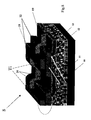
- the transmission conductive layer 21 of the transistor mesh and the spacer 20 serving as gate electrode must be electrically connected and this can easily occur by creating a polysilicon connection bridge 22 as shown in figure 8; in this figure, components and signals common to figures 7 and 6 will maintain the same reference identifiers.
- the speed of the device and the propagation mode of the driving signal will depend on the number of polysilicon connection bridges 22 and on their mutual distance.
- the invention provides the deposition, above the thick oxide 16, of a polysilicon layer 21, suitably doped and of suitable thickness.
- a polysilicon layer 21 suitably doped and of suitable thickness.
- An anisotropic etching follows of the polysilicon 21, suitably masked by means of photolithographic techniques, follows so as to form a spacer of said material which, having filled in the pre-existing cavities, takes the name of recess spacer 20.
- lithographic techniques allows to define both polysilicon paths overhanging the thick dielectric 16 (gate electrode on thick dielectric), and interconnection bridges 22, always in polysilicon, between the overhanging areas of the thick dielectric 16 and the areas with gate oxide, i.e. gate electrode on thin oxide.
- the area below the recess spacer 20 is advantageously used for the formation of the channel.
- the aforesaid polysilicon bridges 22 allow to distribute the signal propagated through the gate electrode on the thick dielectric towards the gate electrode on the thin oxide.
- the peculiarity of the invention consists in the self-alignment between the area of laterally etched thick dielectric 16 and the channel area.
- the process for the realisation of high integration density power MOS devices comprises the following steps:
- This etching step allows to laterally etch the thick dielectric layer 16 with respect to the nitride portions 19 used as hard mask.
- the process must be carried out so as to ensure a high etching selectivity between the thick dielectric layer 16 and the nitride portions 19 used as hard mask.
- FIG. 9 An enlarged vertical section view of a layered structure of a high integration density power MOS device realised at the end of the oxide lateral etching step is shown in figure 9, wherein it is evident that the process leads to the formation of a T-like structure with creation of opposite cavities [undercut] under the nitride portions 19.
- the lateral etching step can be realised by means of chemical solutions based on hydrofluoric acid or chemical solutions based on phosphoric acid or with a suitable isotropic etching in dry.
- a lateral etching step can be realised by means of an etching "in wet” with solutions based on hydrofluoric acid HF.
- BOE solutions Bovine Oxide Etcher
- etching speed 950 A/min
- etching unevenness 5%. This allows to control well the recession of the thick dielectric layer 16 with respect to the overhanging nitride portions 19, given that the nitride is not etched in solutions based on HF.
- the process provides further steps of:
- Figure 10 shows an image obtained by means of scanning electron microscopy [Scanning Electron Microscope] (SEM), of a layered structure of a power MOS device after the lateral etching of the thick dielectric layer 16 and the polysilicon 24 deposition.
- SEM scanning electron microscopy
- the self-alignment of the spacer 20 serving as gate electrode and especially the self-alignment of the body 12 and source 13 diffusions make the photolithography definition realising the initial thick dielectric structure less critical.
- the formation of the recess spacer 20 serving as gate electrode occurs in a process carried out without masking.
- the formation of the recess spacer 20 serving as gate electrode occurs in a process with masking.
- the method further provides the steps of:
- the process is carried out by means of an etching in plasma.
- an etching in plasma By exploiting the high anisotropy it is possible to define, in a simultaneous way, the spacer 20 serving as gate electrode, in correspondence with the step created by the laterally etched thick dielectric layer 16 and the polysilicon transmission conductive layers 21, in the regions masked with the resist 23.
- the spacer 20 serving as gate electrode, in correspondence with the step created by the laterally etched thick dielectric layer 16 and the polysilicon transmission conductive layers 21, in the regions masked with the resist 23.
- the nitride portions 19 and the gate oxide thin layer 15 uncovered at the end of the process will be used as stopping layers (and for the endpoint reading).
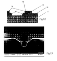
- FIG. 12 An enlarged vertical section view of a layered structure of a power MOS device, further to the anisotropic etching step described is shown in figure 12.
- the corresponding polysilicon recess spacer 20 serving as gate electrode can be seen in figure 13, wherein a section is shown obtained by means of scanning electron microscopy (SEM), of a layered structure of a power MOS device, further to the anisotropic etching step described.
- SEM scanning electron microscopy
- An advantage of the process proposed consists in the possibility of converting the polysilicon layer 24 on the thick dielectric into a suitable silicide (only by way of example cobalt silicide) in an almost complete way, without however risking damaging effects of the gate oxide or of mechanical stress.
- the process according to the invention solves the technical problem and it attains several advantages with respect to the prior art; the first of which is that of being compatible with the technologies VLSI.
- the process in fact, does not require particular alignment restrictions between the various masks necessary for the formation of the elementary MOS, avoiding premature breakdown problems.
- the margin L shown in figure 2 of the prior art description is in fact ensured not by an alignment between the two masks but by a deposition and etching process.
- the physical separation between the polysilicon of the transmission conductive layer (21) and the one placed on the gate oxide allows to transform the whole polysilicon thickness into a silicide without problems on the gate oxide (faultiness or mechanical stress).
Landscapes
- Insulated Gate Type Field-Effect Transistor (AREA)
- Engineering & Computer Science (AREA)
- Electrodes Of Semiconductors (AREA)
- Physics & Mathematics (AREA)
- Condensed Matter Physics & Semiconductors (AREA)
- General Physics & Mathematics (AREA)
- Manufacturing & Machinery (AREA)
- Computer Hardware Design (AREA)
- Microelectronics & Electronic Packaging (AREA)
- Power Engineering (AREA)
- Element Separation (AREA)
Priority Applications (1)
| Application Number | Priority Date | Filing Date | Title |
|---|---|---|---|
| EP10011934A EP2302684A3 (de) | 2004-11-19 | 2005-11-18 | MOS-Leistungsanordnung |
Applications Claiming Priority (1)
| Application Number | Priority Date | Filing Date | Title |
|---|---|---|---|
| IT002243A ITMI20042243A1 (it) | 2004-11-19 | 2004-11-19 | Processo per la realizzazione di un dispositivo mos di potenza ad alta densita' di integrazione |
Related Child Applications (1)
| Application Number | Title | Priority Date | Filing Date |
|---|---|---|---|
| EP10011934.6 Division-Into | 2010-09-30 |
Publications (3)
| Publication Number | Publication Date |
|---|---|
| EP1659637A2 true EP1659637A2 (de) | 2006-05-24 |
| EP1659637A3 EP1659637A3 (de) | 2006-07-19 |
| EP1659637B1 EP1659637B1 (de) | 2011-01-12 |
Family
ID=36088155
Family Applications (2)
| Application Number | Title | Priority Date | Filing Date |
|---|---|---|---|
| EP05025287A Expired - Lifetime EP1659637B1 (de) | 2004-11-19 | 2005-11-18 | Verfahren zur Herstellung einer MOS-Leistungsanordnung |
| EP10011934A Withdrawn EP2302684A3 (de) | 2004-11-19 | 2005-11-18 | MOS-Leistungsanordnung |
Family Applications After (1)
| Application Number | Title | Priority Date | Filing Date |
|---|---|---|---|
| EP10011934A Withdrawn EP2302684A3 (de) | 2004-11-19 | 2005-11-18 | MOS-Leistungsanordnung |
Country Status (4)
| Country | Link |
|---|---|
| US (2) | US7601610B2 (de) |
| EP (2) | EP1659637B1 (de) |
| DE (1) | DE602005025845D1 (de) |
| IT (1) | ITMI20042243A1 (de) |
Families Citing this family (7)
| Publication number | Priority date | Publication date | Assignee | Title |
|---|---|---|---|---|
| US9184278B2 (en) * | 2013-12-09 | 2015-11-10 | Micrel, Inc. | Planar vertical DMOS transistor with a conductive spacer structure as gate |
| US9178054B2 (en) | 2013-12-09 | 2015-11-03 | Micrel, Inc. | Planar vertical DMOS transistor with reduced gate charge |
| US9607635B1 (en) * | 2016-04-22 | 2017-03-28 | International Business Machines Corporation | Current perpendicular-to-plane sensors having hard spacers |
| US9947348B1 (en) | 2017-02-28 | 2018-04-17 | International Business Machines Corporation | Tunnel magnetoresistive sensor having leads supporting three-dimensional current flow |
| US10803889B2 (en) | 2019-02-21 | 2020-10-13 | International Business Machines Corporation | Apparatus with data reader sensors more recessed than servo reader sensor |
| US11074930B1 (en) | 2020-05-11 | 2021-07-27 | International Business Machines Corporation | Read transducer structure having an embedded wear layer between thin and thick shield portions |
| US11114117B1 (en) | 2020-05-20 | 2021-09-07 | International Business Machines Corporation | Process for manufacturing magnetic head having a servo read transducer structure with dielectric gap liner and a data read transducer structure with an embedded wear layer between thin and thick shield portions |
Family Cites Families (27)
| Publication number | Priority date | Publication date | Assignee | Title |
|---|---|---|---|---|
| US4055884A (en) | 1976-12-13 | 1977-11-01 | International Business Machines Corporation | Fabrication of power field effect transistors and the resulting structures |
| US4318759A (en) * | 1980-07-21 | 1982-03-09 | Data General Corporation | Retro-etch process for integrated circuits |
| US4748103A (en) * | 1986-03-21 | 1988-05-31 | Advanced Power Technology | Mask-surrogate semiconductor process employing dopant protective region |
| EP0518418A1 (de) * | 1991-06-10 | 1992-12-16 | Koninklijke Philips Electronics N.V. | Verfahren zum Herstellen einer Halbleiteranordnung, wobei in einer Oberfläche eines Siliziumkörpers durch Oxidation Feldoxidgebiete gebildet werden |
| US5430314A (en) | 1992-04-23 | 1995-07-04 | Siliconix Incorporated | Power device with buffered gate shield region |
| EP0693773B1 (de) | 1994-07-14 | 2005-02-09 | STMicroelectronics S.r.l. | VDMOS-Leistungsbauteil und Verfahren zur Herstellung desselben |
| US5795793A (en) * | 1994-09-01 | 1998-08-18 | International Rectifier Corporation | Process for manufacture of MOS gated device with reduced mask count |
| US5510281A (en) * | 1995-03-20 | 1996-04-23 | General Electric Company | Method of fabricating a self-aligned DMOS transistor device using SiC and spacers |
| JP3166148B2 (ja) | 1995-07-11 | 2001-05-14 | 横河電機株式会社 | 半導体装置 |
| EP0772242B1 (de) * | 1995-10-30 | 2006-04-05 | STMicroelectronics S.r.l. | Leistungsbauteil in MOS-Technologie mit einer einzelnen kritischen Grösse |
| EP0817274B1 (de) | 1996-07-05 | 2004-02-11 | STMicroelectronics S.r.l. | Asymmetrische MOS-Technologie-Leistungsanordnung |
| US6025230A (en) * | 1997-11-06 | 2000-02-15 | Mageposer Semiconductor Corporation | High speed MOSFET power device with enhanced ruggedness fabricated by simplified processes |
| US6187694B1 (en) * | 1997-11-10 | 2001-02-13 | Intel Corporation | Method of fabricating a feature in an integrated circuit using two edge definition layers and a spacer |
| GB9726829D0 (en) | 1997-12-19 | 1998-02-18 | Philips Electronics Nv | Power semiconductor devices |
| US6107649A (en) * | 1998-06-10 | 2000-08-22 | Rutgers, The State University | Field-controlled high-power semiconductor devices |
| US6215152B1 (en) * | 1998-08-05 | 2001-04-10 | Cree, Inc. | MOSFET having self-aligned gate and buried shield and method of making same |
| KR20000051294A (ko) * | 1999-01-20 | 2000-08-16 | 김덕중 | 전기적 특성이 향상된 디모스 전계 효과 트랜지스터 및 그 제조 방법 |
| JP4917709B2 (ja) | 2000-03-06 | 2012-04-18 | ローム株式会社 | 半導体装置 |
| US6710405B2 (en) | 2001-01-17 | 2004-03-23 | Ixys Corporation | Non-uniform power semiconductor device |
| US6756644B2 (en) * | 2001-03-28 | 2004-06-29 | International Rectifier Corporation | Ultra low QGD power MOSFET |
| DE10131917A1 (de) * | 2001-07-02 | 2003-01-23 | Infineon Technologies Ag | Verfahren zur Erzeugung einer stufenförmigen Struktur auf einem Substrat |
| US6706591B1 (en) * | 2002-01-22 | 2004-03-16 | Taiwan Semiconductor Manufacturing Company | Method of forming a stacked capacitor structure with increased surface area for a DRAM device |
| US7045845B2 (en) * | 2002-08-16 | 2006-05-16 | Semiconductor Components Industries, L.L.C. | Self-aligned vertical gate semiconductor device |
| US6979863B2 (en) * | 2003-04-24 | 2005-12-27 | Cree, Inc. | Silicon carbide MOSFETs with integrated antiparallel junction barrier Schottky free wheeling diodes and methods of fabricating the same |
| JP4179147B2 (ja) | 2003-11-28 | 2008-11-12 | 株式会社デンソー | 炭化珪素半導体装置 |
| US7105410B2 (en) * | 2004-04-09 | 2006-09-12 | Analog And Power Electronics Corp. | Contact process and structure for a semiconductor device |
| US20060086974A1 (en) | 2004-10-26 | 2006-04-27 | Power Integrations, Inc. | Integrated circuit with multi-length power transistor segments |
-
2004
- 2004-11-19 IT IT002243A patent/ITMI20042243A1/it unknown
-
2005
- 2005-11-18 DE DE602005025845T patent/DE602005025845D1/de not_active Expired - Lifetime
- 2005-11-18 EP EP05025287A patent/EP1659637B1/de not_active Expired - Lifetime
- 2005-11-18 EP EP10011934A patent/EP2302684A3/de not_active Withdrawn
- 2005-11-21 US US11/285,742 patent/US7601610B2/en not_active Expired - Fee Related
-
2009
- 2009-09-01 US US12/551,999 patent/US8013384B2/en not_active Expired - Fee Related
Non-Patent Citations (1)
| Title |
|---|
| None |
Also Published As
| Publication number | Publication date |
|---|---|
| US20090321826A1 (en) | 2009-12-31 |
| EP1659637B1 (de) | 2011-01-12 |
| EP2302684A3 (de) | 2012-03-14 |
| ITMI20042243A1 (it) | 2005-02-19 |
| US20060138537A1 (en) | 2006-06-29 |
| US7601610B2 (en) | 2009-10-13 |
| EP2302684A2 (de) | 2011-03-30 |
| DE602005025845D1 (de) | 2011-02-24 |
| EP1659637A3 (de) | 2006-07-19 |
| US8013384B2 (en) | 2011-09-06 |
Similar Documents
| Publication | Publication Date | Title |
|---|---|---|
| US11075297B2 (en) | Semiconductor device and method of manufacturing semiconductor device | |
| CN100481503C (zh) | 沟槽栅晶体管及其制造 | |
| US7176137B2 (en) | Method for multiple spacer width control | |
| US6953726B2 (en) | High-density split-gate FinFET | |
| KR100511045B1 (ko) | 리세스된 게이트 전극을 갖는 반도체 소자의 집적방법 | |
| CN102130015B (zh) | 用于高电压场效应晶体管的栅蚀刻工艺 | |
| KR100471189B1 (ko) | 수직채널을 갖는 전계효과 트랜지스터 및 그 제조방법 | |
| US6469345B2 (en) | Semiconductor device and method for manufacturing the same | |
| KR101560012B1 (ko) | 핀 트랜지스터들을 포함하는 시스템들 및 디바이스들, 및 그의 사용, 제조 및 동작 방법 | |
| JP4851080B2 (ja) | Ldmosトランジスタ装置、集積回路およびその製造方法 | |
| US9543298B1 (en) | Single diffusion break structure and cuts later method of making | |
| US8013384B2 (en) | Method for manufacturing a high integration density power MOS device | |
| US9536991B1 (en) | Single diffusion break structure | |
| JP5442921B2 (ja) | ゲート酸化膜の完全性を向上させた半導体トレンチ素子 | |
| CN1502127A (zh) | 半导体器件及其形成工艺 | |
| US6225175B1 (en) | Process for defining ultra-thin geometries | |
| US20010034109A1 (en) | Trench seimconductor devices reduced trench pitch | |
| CN103258741A (zh) | 纳米线场效应晶体管及其形成方法 | |
| KR100956558B1 (ko) | 반도체 기판 내에 좁은 트렌치 형성 방법 및 트렌치 mosfet 형성 방법 | |
| US20150287782A1 (en) | Integrated circuits and methods of fabrication thereof | |
| US7011929B2 (en) | Method for forming multiple spacer widths | |
| TWI277153B (en) | Semiconductor device with recessed channel and method of fabricating the same | |
| KR20050001193A (ko) | 초미세 채널 전계 효과 트랜지스터 및 그 제조방법 | |
| KR20100069954A (ko) | 미세 패턴 형성 방법 및 이를 이용한 트랜지스터 제조 방법 | |
| KR100732305B1 (ko) | 디램 셀 및 그 제조 방법 |
Legal Events
| Date | Code | Title | Description |
|---|---|---|---|
| PUAI | Public reference made under article 153(3) epc to a published international application that has entered the european phase |
Free format text: ORIGINAL CODE: 0009012 |
|
| AK | Designated contracting states |
Kind code of ref document: A2 Designated state(s): AT BE BG CH CY CZ DE DK EE ES FI FR GB GR HU IE IS IT LI LT LU LV MC NL PL PT RO SE SI SK TR |
|
| AX | Request for extension of the european patent |
Extension state: AL BA HR MK YU |
|
| PUAL | Search report despatched |
Free format text: ORIGINAL CODE: 0009013 |
|
| AK | Designated contracting states |
Kind code of ref document: A3 Designated state(s): AT BE BG CH CY CZ DE DK EE ES FI FR GB GR HU IE IS IT LI LT LU LV MC NL PL PT RO SE SI SK TR |
|
| AX | Request for extension of the european patent |
Extension state: AL BA HR MK YU |
|
| 17P | Request for examination filed |
Effective date: 20070117 |
|
| 17Q | First examination report despatched |
Effective date: 20070215 |
|
| AKX | Designation fees paid |
Designated state(s): DE FR GB IT |
|
| RAP1 | Party data changed (applicant data changed or rights of an application transferred) |
Owner name: STMICROELECTRONICS SRL |
|
| GRAP | Despatch of communication of intention to grant a patent |
Free format text: ORIGINAL CODE: EPIDOSNIGR1 |
|
| GRAS | Grant fee paid |
Free format text: ORIGINAL CODE: EPIDOSNIGR3 |
|
| GRAA | (expected) grant |
Free format text: ORIGINAL CODE: 0009210 |
|
| GRAL | Information related to payment of fee for publishing/printing deleted |
Free format text: ORIGINAL CODE: EPIDOSDIGR3 |
|
| GRAS | Grant fee paid |
Free format text: ORIGINAL CODE: EPIDOSNIGR3 |
|
| AK | Designated contracting states |
Kind code of ref document: B1 Designated state(s): DE FR GB IT |
|
| REG | Reference to a national code |
Ref country code: GB Ref legal event code: FG4D |
|
| REF | Corresponds to: |
Ref document number: 602005025845 Country of ref document: DE Date of ref document: 20110224 Kind code of ref document: P |
|
| REG | Reference to a national code |
Ref country code: DE Ref legal event code: R096 Ref document number: 602005025845 Country of ref document: DE Effective date: 20110224 |
|
| PLBE | No opposition filed within time limit |
Free format text: ORIGINAL CODE: 0009261 |
|
| STAA | Information on the status of an ep patent application or granted ep patent |
Free format text: STATUS: NO OPPOSITION FILED WITHIN TIME LIMIT |
|
| 26N | No opposition filed |
Effective date: 20111013 |
|
| REG | Reference to a national code |
Ref country code: DE Ref legal event code: R097 Ref document number: 602005025845 Country of ref document: DE Effective date: 20111013 |
|
| GBPC | Gb: european patent ceased through non-payment of renewal fee |
Effective date: 20111118 |
|
| REG | Reference to a national code |
Ref country code: DE Ref legal event code: R119 Ref document number: 602005025845 Country of ref document: DE Effective date: 20120601 |
|
| PG25 | Lapsed in a contracting state [announced via postgrant information from national office to epo] |
Ref country code: GB Free format text: LAPSE BECAUSE OF NON-PAYMENT OF DUE FEES Effective date: 20111118 |
|
| PGFP | Annual fee paid to national office [announced via postgrant information from national office to epo] |
Ref country code: FR Payment date: 20130107 Year of fee payment: 8 |
|
| PG25 | Lapsed in a contracting state [announced via postgrant information from national office to epo] |
Ref country code: DE Free format text: LAPSE BECAUSE OF NON-PAYMENT OF DUE FEES Effective date: 20120601 |
|
| PG25 | Lapsed in a contracting state [announced via postgrant information from national office to epo] |
Ref country code: IT Free format text: LAPSE BECAUSE OF NON-PAYMENT OF DUE FEES Effective date: 20121118 |
|
| REG | Reference to a national code |
Ref country code: FR Ref legal event code: ST Effective date: 20140731 |
|
| PG25 | Lapsed in a contracting state [announced via postgrant information from national office to epo] |
Ref country code: FR Free format text: LAPSE BECAUSE OF NON-PAYMENT OF DUE FEES Effective date: 20131202 |