EP1640992A2 - Magnetische Speicheranordnung - Google Patents
Magnetische Speicheranordnung Download PDFInfo
- Publication number
- EP1640992A2 EP1640992A2 EP05021012A EP05021012A EP1640992A2 EP 1640992 A2 EP1640992 A2 EP 1640992A2 EP 05021012 A EP05021012 A EP 05021012A EP 05021012 A EP05021012 A EP 05021012A EP 1640992 A2 EP1640992 A2 EP 1640992A2
- Authority
- EP
- European Patent Office
- Prior art keywords
- magnetic
- magnetic yoke
- magnetoresistive element
- yoke
- open ends
- Prior art date
- Legal status (The legal status is an assumption and is not a legal conclusion. Google has not performed a legal analysis and makes no representation as to the accuracy of the status listed.)
- Withdrawn
Links
Images




Classifications
-
- G—PHYSICS
- G11—INFORMATION STORAGE
- G11C—STATIC STORES
- G11C11/00—Digital stores characterised by the use of particular electric or magnetic storage elements; Storage elements therefor
- G11C11/02—Digital stores characterised by the use of particular electric or magnetic storage elements; Storage elements therefor using magnetic elements
- G11C11/16—Digital stores characterised by the use of particular electric or magnetic storage elements; Storage elements therefor using magnetic elements using elements in which the storage effect is based on magnetic spin effect
Definitions
- the present invention relates to a magnetic storage device that can store information therein by using a magnetoresistive effect.
- MRAM magnetic random access memory
- the magnetic storage device is required to efficiently perform writing to a magnetoresistive element in order to achieve improvement of an operation speed, reduction of writing current, and the like.
- a magnetic storage device is proposed that includes an approximately annular magnetic yoke for concentrating a magnetic flux generated around a wiring on a magnetoresistive element (see Japanese Patent Laid-Open Publications Nos. 2000-90658 and 2004-128430, for example).
- the intensity of a magnetic field generated from the magnetic yoke is determined by its material, shape, and the like. However, there was conventionally almost no specific proposal regarding the shape of the magnetic yoke and a relationship between the intensity of the magnetic field generated from the magnetic yoke and the shape of the magnetic yoke was not made apparent.
- various exemplary embodiments of this invention provide a magnetic storage device that can materialize a shape of a magnetic yoke and can increase a magnetic field generated from the magnetic yoke by optimizing the shape of the magnetic yoke so as to reduce writing current.
- the inventor of the present invention found the magnetic storage device that could materialize the shape of the magnetic yoke and could increase the magnetic field generated from the magnetic yoke by optimizing the shape of the magnetic yoke so as to reduce the writing current.
- the shape of the magnetic yoke can be materialized. Moreover, the magnetic field generated from the magnetic yoke can be increased by optimization of the shape of the magnetic yoke, thereby reducing the writing current.
- a magnetic storage device a plurality of storage areas each of which includes: a magnetoresistive element having a sensitive magnetic layer in which a magnetizing direction is changed by an external magnetic field; a wiring that provides the external magnetic field to the sensitive magnetic layer by writing current; and an approximately annular magnetic yoke having at least a pair of open ends opposed to each other with a gap interposed therebetween, the magnetic yoke being arranged to surround an outer circumference of the wiring at a portion in an extending direction of the wiring.
- a maximum thickness of each of the open ends of the magnetic yoke in a diameter direction of the magnetic yoke is set to be larger than a maximum thickness of the sensitive magnetic layer of the magnetoresistive element in the diameter direction of the magnetic yoke. Due to this structure, the present invention can materialize a shape of the magnetic yoke, and can increase a magnetic field generated from the magnetic yoke by optimization of the shape of the magnetic yoke so as to reduce writing current.
- a magnetic storage device includes a plurality of storage areas each of which includes: a magnetoresistive element having a sensitive magnetic layer in which a magnetizing direction is changed by an external magnetic field; a wiring that provides the external magnetic field to the sensitive magnetic layer by writing current; and an approximately annular magnetic yoke having at least a pair of open ends opposed to each other with a gap interposed therebetween, the magnetic yoke being arranged to surround an outer circumference of the wiring at a portion in an extending direction of the wiring.
- a product of a maximum thickness of each of the open ends of the magnetic yoke in a diameter direction of the magnetic yoke and saturated magnetization in the magnetic yoke is set to be larger than a product of a maximum thickness of the sensitive magnetic layer of the magnetoresistive element in the diameter direction of the magnetic yoke and saturated magnetization in the sensitive magnetic layer. Due to this, the present invention can overcome the above problem.
- a magnetic storage device includes a plurality of storage areas each of which includes: a magnetoresistive element having a sensitive magnetic layer in which a magnetizing direction is changed by an external magnetic field; a wiring that provides the external magnetic field to the sensitive magnetic layer by writing current; and an approximately annular magnetic yoke having at least a pair of open ends opposed to each other with a gap interposed therebetween, the magnetic yoke being arranged to surround an outer circumference of the wiring at a portion in an extending direction of the wiring.
- a width of each of the open ends of the magnetic yoke in an axial direction of the magnetic yoke is set to be equal to or larger than a width of the sensitive magnetic layer of the magnetoresistive element in the axial direction of the magnetic yoke and is set to be three times or less a length of the gap of the magnetic yoke in a circumferential direction of the magnetic yoke. Due to this, the present invention can overcome the above problem.
- a magnetic storage device includes a plurality of storage areas each of which includes: a magnetoresistive element having a sensitive magnetic layer in which a magnetizing direction is changed by an external magnetic field; a wiring that provides the external magnetic field to the sensitive magnetic layer by writing current; and an approximately annular magnetic yoke having at least a pair of open ends opposed to each other with a gap interposed therebetween, the magnetic yoke being arranged to surround an outer circumference of the wiring at a portion in an extending direction of the wiring.
- a length of the gap of the magnetic yoke in a circumferential direction of the magnetic yoke is set to be equal to or larger than a length of the sensitive magnetic layer of the magnetoresistive element in the circumferential direction of the magnetic yoke and is set to be equal to or smaller than 1 ⁇ m. Due to this, the present invention can overcome the above object.
- a magnetic storage device according to a first exemplary embodiment of the present invention is now described in detail, with reference to the drawings.
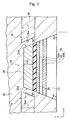
- the magnetic storage device 10 of the first exemplary embodiment includes a plurality of storage areas. As shown in Figs. 1 and 2, each storage area includes: a wiring 12 that provides an external magnetic field by a writing current; an approximately annular magnetic yoke 18 having a pair of open ends 14 and 16 opposed to each other with a gap interposed therebetween; and a magnetoresistive element 20 having a second magnetic layer (sensitive magnetic layer) 28 in which a magnetizing direction is changed by the external magnetic field.
- the magnetic yoke 18 is arranged to surround an outer circumference of the wiring 12 at a portion in an extending direction of the wiring 12.
- the wiring 12 is used for writing of magnetizing information to the magnetoresistive element 20 and is arranged to pass near an axial center 01 of the magnetic yoke 18 in the first exemplary embodiment.
- the magnetic yoke 18 is formed of Permalloy (NiFe) in the first exemplary embodiment as one unit that is magnetically and mechanically continuous.
- the structure and material of the magnetic yoke 18 are not limited thereto.
- ferrocobalt (CoFe) can be used as the material of the magnetic yoke 18.
- the magnetoresistive element 20 includes an antiferromagnetic layer 22, a first magnetic layer 24, a non-magnetic layer 26, and a second magnetic layer 28 that are sequentially formed.
- the magnetoresistive element 20 can be easily manufactured by depositing the antiferromagnetic layer 22, the first magnetic layer 24, the non-magnetic layer 26, and the second magnetic layer 28 on a substrate (not shown) in that order or a reversed order by sputtering or the like.
- the antiferromagnetic layer 22 is formed of a disordered alloy IrMn having a thickness of 90 nm in the first exemplary embodiment.
- a disordered alloy RuRhMn or an ordered alloy PtMn may be used for the antiferromagnetic layer 22, for example.
- the first magnetic layer 24 is a so-called fixed layer (pinned layer) in which an orientation of magnetization is fixed.
- the first magnetic layer 24 is formed to be in contact with the antiferromagnetic layer 22.
- an exchange-coupling magnetic field is generated at an interface between the antiferromagnetic layer 22 and the first magnetic layer 24, thereby the orientation of magnetization in the first magnetic layer 24 is fixed.
- the first magnetic layer 24 has a three-layer structure including a magnetic layer 30A, a non-magnetic conductive layer 32, and a magnetic layer 30B that are sequentially formed, in order to enhance a fixing force of the antiferromagnetic layer 22 for fixing the magnetizing direction in the first magnetic layer 24.
- the magnetic layer 30A is formed of a ferrocobalt alloy (CoFe) and has a thickness of 16 nm
- the non-magnetic conductive layer 32 is formed of ruthenium (Ru) and has a thickness of 8.5 nm
- the magnetic layer 30B is formed of a ferrocobalt alloy (CoFe) and has a thickness of 12 nm.
- cobalt (Co), cobalt-platinum alloys (CoPt), and nickel-iron-cobalt alloys (NiFeCo) can be used for the magnetic layers 30A and 30B, for example.
- the non-magnetic layer 26 is formed on the first magnetic layer 24.
- the non-magnetic layer 26 is formed of aluminum oxide (Al 2 O 3 ) having a thickness of 9 nm.
- the second magnetic layer 28 is a so-called sensitive magnetic layer (free layer) in which an orientation of magnetization can be changed.
- the second magnetic layer 28 is formed by forming a layer of a ferronickel alloy (NiFe) having a thickness of 30 nm on a layer of a ferrocobalt (CoFe) alloy having a thickness of 15 nm.
- the open ends 14 and 16 of the magnetic yoke 18 are arranged at approximately the same level as the second magnetic layer 28.
- the open ends 14 and 16 of the magnetic yoke 18 are arranged at approximately the same level as the second magnetic layer 28.
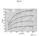
- Fig. 4 shows a result of measurement in which a maximum thickness T1 of each open end 14 or 16 of the magnetic yoke 18 and a ratio of magnetization reversal (Mx/MS2) in the second magnetic layer 28 of the magnetoresistive element 20 were measured when a maximum thickness T2 of the second magnetic layer 28 in a diameter direction Y of the magnetic yoke 18 was 5 nm, 10 nm, and 15 nm.
- the ratio of magnetization reversal (Mx/MS2) represents a ratio of magnetized components Mx in a direction of an axis of easy magnetization in the second magnetic layer 28 to saturated magnetization MS2 in the second magnetic layer 28.
- the maximum thickness T1 of each open end 14 or 16 is thicker than necessary, it is more difficult to saturate magnetization in the magnetic yoke 18.
- the maximum thickness T1 of each open end 14 or 16 be about 20 times or less the maximum thickness T2 of the second magnetic layer 28 of the magnetoresistive element 20 (T1 ⁇ T2 x 20) .
- a magnetic flux generated in the gap of the magnetic yoke 18 becomes larger in proportion to saturated magnetization MS1 in the magnetic yoke 18 and the thickness T1 of each of the open ends 14 and 16 of the magnetic yoke 18 in the diameter direction of the magnetic yoke 18.
- a demagnetization field in the second magnetic layer 28 of the magnetoresistive element 20 becomes larger in proportion to the thickness T2 of the second magnetic layer 28 and the saturated magnetization MS2 in the second magnetic layer 28.
- the magnetization reversal in the second magnetic layer 28 can be made controllable by making a product of the maximum thickness T1 of each of the open ends 14 and 16 of the magnetic yoke 18 and the saturated magnetization MS1 in the magnetic yoke 18 equal to or larger than a product of the maximum thickness T2 of the second magnetic layer 28 of the magnetoresistive element 20 and the saturated magnetization MS2 in the second magnetic layer 28 (T1 ⁇ MS1 ⁇ T2 ⁇ MS2).
- Axes of easy magnetization of the first and second magnetic layers 24 and 28 are set in such a manner that a stable magnetizing state in each of those layers is parallel or antiparallel to the axis of easy magnetization, and are set to be approximately coincident with an orientation of magnetic field lines inside the magnetic yoke 18 near a pair of open ends 14 and 16 of the magnetic yoke 18. Due to this structure, the orientation of the magnetic field lines inside the magnetic yoke 18 is parallel or antiparallel to the magnetizing direction in the second magnetic layer 28. Thus, the amount of the generated magnetic field that is required for magnetization reversal in the second magnetic layer 28 can be made minimum. It is preferable that the axes of easy magnetization of the first magnetic layer 24 and the second magnetic layer 28 be parallel to each other in order to make the magnetizing directions stable in a state where the magnetizing directions are parallel or antiparallel to each other.
- the magnetoresistive element 20 is arranged in such a manner that a pair of side faces 20A and 20B thereof (i.e., faces close to the magnetic yoke 18) are at least partially opposed to end faces 14A and 16A of a pair of open ends 14 and 16 of the magnetic yoke 18, respectively.
- a width W1 of each open end 14 or 16 of the magnetic yoke 18 in an axial direction Z of the magnetic yoke 18 is equal to or larger than a width W2 of the second magnetic layer 28 of the magnetoresistive element 20 in the axial direction Z of the magnetic yoke 18 (W1 ⁇ W2) in order to prevent distribution of the magnetic flux associated with the magnetoresistive element 20 from becoming uneven. It is preferable that the width W1 of each open end 14 or 16 of the magnetic yoke 18 be three times or less a length L1 of the gap of the magnetic yoke 18 in a circumferential direction X of the magnetic yoke 18 (W1 ⁇ L1 ⁇ 3).
- the length L1 of the gap of the magnetic yoke 18 is set to be equal to or larger than a length L2 of the second magnetic layer 28 of the magnetoresistive element 20 in the circumferential direction X of the magnetic yoke 18 and be equal to or smaller than 1 ⁇ m.
- the magnetic yoke 18 may be usually conductive, it has any form as long as the magnetoresistive element 20 can arranged within the gap. The magnetic yoke 18 may be in contact with the second magnetic layer 28 of the magnetoresistive element 20.
- the end faces 14A and 16A of the open ends 14 and 16 of the magnetic yoke 18 and the side faces 20A and 20B of the magnetoresistive element 20 are inclined at predetermined angles of ⁇ A, ⁇ B, ⁇ C, and ⁇ D, respectively, in such a manner that a distance between the end faces 14A and 16A and a distance between the side faces 20A and 20B become larger downwards.
- all of the inclination angles ⁇ A and ⁇ B of the end faces 14A and 16A of the open ends 14 and 16 of the magnetic yoke 18 and the inclination angles ⁇ C and ⁇ D of the side faces 20A and 20A of the magnetoresistive element 20 are set to approximately the same angle that is equal to or larger than 20 degrees and is smaller than 90 degrees.
- the side faces 20A and 20B of the magnetoresistive element 20 can be processed to be inclined by ion milling, reactive ion etching (RIE), or the like.
- ion milling discharge is generated by applying a voltage to argon gas under a predetermined pressure, thereby generating plasma. Then, a voltage of about 100 to 500 V is applied as an acceleration voltage to ions in the plasma so as to accelerate those ions in a predetermined direction.
- the thus accelerated ions ION are irradiated toward a surface of the magnetoresistive element 20 as shown in Fig. 4A to cause collision of the ions ION against the magnetoresistive element 20,.
- Fig. 4A reactive ion etching
- the magnetoresistive element 20 outside a region masked with a resist pattern 34 is removed by a sputtering phenomenon caused by the collision.
- the side faces 20A and 20B of the magnetoresistive element 20 can be inclined at an angle of about 20 degrees to about 90 degrees by controlling an irradiation angle and an irradiation time of the ions ION.
- anisotropic etching can be performed with high precision due to sputtering using ions and chemical reaction of etching gas that is changed to plasma.
- This reactive ion etching can incline the side faces 20A and 20B of the magnetoresistive element 20 at an angle of about 20 degrees to about 80 degrees.
- a cross-sectional area of a top of each open end 14 or 16 of the magnetic yoke 18 becomes smaller.
- saturation of magnetization occurs rapidly at the top of the magnetic yoke 18 and a magnetic flux can be more easily generated from the magnetic yoke 18.
- broadening of regions of the end faces 14A and 16A occurs in this case.
- the smaller inclination angle is not realistic and is unfavorable in terms of obtaining a high-density device. For this reason, it is preferable to design the inclination angle to be the most appropriate angle in a region of from 20 to 90 degrees in accordance with needs.
- an insulation layer 36 is formed from a non-conductive material such as aluminum oxide (Al 2 O 3 ) to have an approximately uniform thickness on the magnetoresistive element 20. Then, the open ends 14 and 16 of the magnetic yoke 18 are formed.
- a non-conductive material such as aluminum oxide (Al 2 O 3 )
- the second magnetic layer 28 can serve as a recording layer for storing magnetizing information therein.
- the shape of the magnetic yoke 18 is optimized in the magnetic storage device 10 of the first embodiment in various ways. More specifically, (1) the maximum thickness T1 of each of the open ends 14 and 16 of the magnetic yoke 18 in the diameter direction Y of the magnetic yoke 18 is set to be larger than the maximum thickness T2 of the second magnetic layer (sensitive magnetic layer) 28 of the magnetoresistive element 20 in the diameter direction Y of the magnetic yoke 18, (2) the product of the maximum thickness T1 of each open end 14 or 16 of the magnetic yoke 18 and the saturated magnetization MS1 in the magnetic yoke 18 is set to be larger than the product of the maximum thickness T2 of the second magnetic layer 28 of the magnetoresistive element 20 and the saturated magnetization MS2 of the second magnetic layer 28, (3) the width W1 of each open end 14 or 16 of the magnetic yoke 18 in the axial direction Z of the magnetic yoke 18 is set to be equal to or larger than the width W2 of the second magnetic layer 28 of the magnetoresistive element 20
- the shape of the magnetic yoke can be materialized. Moreover, the magnetic field generated from the magnetic yoke can be increased by optimization of the shape of the magnetic yoke, thereby reducing writing current.
- the side faces 20A and 20B of the magnetoresistive element 20 are at least partially opposed to the end faces 14A and 16A of the open ends of the magnetic yoke 18, respectively, and the side faces 20A and 20B of the magnetoresistive element 20 and the end faces 14A and 16A of the open ends 14 and 16 of the magnetic yoke 18 have predetermined inclination angles ⁇ A, ⁇ B, ⁇ C, and ⁇ D, respectively.
- surface areas of the end faces 14A and 16A of the open ends 14 and 16 of the magnetic yoke 18 and the side faces 20A and 20B of the magnetoresistive element 20 can be made larger.
- the magnetic flux of the magnetic field directed from the magnetic yoke 18 to the magnetoresistive element 20 can be increased and the writing current can be further reduced.
- the cross-sectional area of the top of each open end 14 or 16 of the magnetic yoke 18 can be made smaller.
- saturation of magnetization at the top of the magnetic yoke 18 can occur rapidly and therefore a magnetic flux can be more easily generated from the magnetic yoke 18. This can increase the magnetic flux of the magnetic field directed to the magnetoresistive element 20.
- the side faces 20A and 20B of the magnetoresistive element 20 and the end faces 14A and 16A of the open ends 14 and 16 of the magnetic yoke 18 are inclined at approximately the same angle, it is easy to process them. Furthermore, it is possible to uniformly direct the magnetic flux of the magnetic field generated from the magnetic yoke 18 to the magnetoresistive element 20. Therefore, the writing current can be further reduced. In addition, the magnitude of the magnetic flux directed to the magnetoresistive element 20 and a timing at which the magnetic flux is applied can be made approximately the same for a plurality of storage areas (cells). This can suppress variation in writing characteristics.
- magnetic resistance of the magnetic yoke 18 can be reduced. This equalizes the magnetic field lines passing inside the magnetic yoke 18, thus suppressing turbulence caused by the magnetic resistance.
- the wiring 12 is arranged to pass near the axial center 01 of the magnetic yoke 18, the magnetic flux of the magnetic field generated from the wiring 12 can be efficiently directed to the inside of the magnetic yoke 18. Thus, even when the magnitude of the writing current is small, writing can be performed efficiently and stably.
- the side faces 20A and 20B of the magnetoresistive element 20 are at least partially opposed to the end faces 14A and 16A of the open ends 14 and 16 of the magnetic yoke 18, respectively, and the orientation of the magnetic field lines inside the magnetic yoke 18 near the open ends 14 and 16 of the magnetic yoke 18 is approximately coincident with the orientation of the axis of easy magnetization of the magnetoresistive element 20.
- the magnetization in the magnetoresistive element 20 can be efficiently reversed while the magnetic storage device 10 can have a compact and simple structure, and the writing current can be reduced as compared with that in a conventional magnetic storage device.
- a wrong operation caused by tilt of magnetization in the sensitive magnetic layer because of an effect of residual magnetization in the magnetic yoke 18 does not occur.
- the magnetic storage device 10 can perform writing more stably.
- the insulation layer 36 that is formed of a non-conductive material and has an approximately uniform thickness is provided between a pair of side faces 20A and 20B of the magnetoresistive element 20 and the end faces 14A and 16A of the pair of open ends 14 and 16 of the magnetic yoke 18, a distance between the magnetoresistive element 20 and the magnetic yoke 18 can be kept constant. Thus, it is possible to make the intensity of the magnetic flux generated from the magnetic yoke 18 uniform and allow that magnetic flux to effectively affect the magnetoresistive element 20.
- the magnetoresistive element 20 includes at least the antiferromagnetic layer 22, the first magnetic layer 24, the non-magnetic layer 26, and the second magnetic layer 28 that are sequentially formed.
- the magnetoresistive element 20 can achieve a magnetoresistive effect in a low magnetic field. It is also possible to easily determine the magnetizing direction in the sensitive magnetic layer.
- the first magnetic layer 24 has a three-layer structure including the magnetic layer 30A, the non-magnetic conductive layer 32, and the magnetic layer 30B.
- the magnetizing direction in the first magnetic layer 24 serving as the fixed layer is not made unstable by a magnetic field generated from a gap in the magnetic yoke 18. Therefore, it is possible to make the orientation of magnetization in the fixed layer harder to reverse.
- the magnetic storage device of the present invention is not limited to the structure, shape, and the like of the magnetic storage device 10 according to the above first exemplary embodiment.
- a magnetic yoke 38 in which its cross-sectional shape in a diameter direction is approximately round, as shown in Fig. 5, or a magnetic yoke 40 in which its cross-sectional shape in the diameter direction is approximately oval, as shown in Fig. 6, may be used in place of the magnetic yoke 18 in the first embodiment, for example.
- the magnetic field lines passing inside the magnetic yoke 38 (40) can be made more uniform and therefore the magnetic field caused by the writing current can be stabilized.
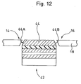
- the magnetic storage device 10 of present invention may be configured such that only faces 44A and 44B of a sensitive magnetic layer 44 that are close to the magnetic yoke 18 (i.e., at least a part of a pair of side faces of the magnetoresistive element 42) may be inclined as in a magnetoresistive element 42 shown in Fig. 7, for example.
- the magnetic storage device 10 of the present invention may be configured such that the inclination angles ⁇ A, ⁇ B, ⁇ C, and ⁇ D may be set to different angles.
Landscapes
- Engineering & Computer Science (AREA)
- Computer Hardware Design (AREA)
- Hall/Mr Elements (AREA)
- Mram Or Spin Memory Techniques (AREA)
- Semiconductor Memories (AREA)
Applications Claiming Priority (1)
| Application Number | Priority Date | Filing Date | Title |
|---|---|---|---|
| JP2004282566A JP2006100424A (ja) | 2004-09-28 | 2004-09-28 | 磁気記憶装置 |
Publications (1)
| Publication Number | Publication Date |
|---|---|
| EP1640992A2 true EP1640992A2 (de) | 2006-03-29 |
Family
ID=35462562
Family Applications (1)
| Application Number | Title | Priority Date | Filing Date |
|---|---|---|---|
| EP05021012A Withdrawn EP1640992A2 (de) | 2004-09-28 | 2005-09-27 | Magnetische Speicheranordnung |
Country Status (4)
| Country | Link |
|---|---|
| US (1) | US7460393B2 (de) |
| EP (1) | EP1640992A2 (de) |
| JP (1) | JP2006100424A (de) |
| CN (1) | CN1770315A (de) |
Cited By (1)
| Publication number | Priority date | Publication date | Assignee | Title |
|---|---|---|---|---|
| US8963544B2 (en) | 2008-09-29 | 2015-02-24 | The Research Institute For Electric And Magnetic Materials | Signal transmission device |
Families Citing this family (6)
| Publication number | Priority date | Publication date | Assignee | Title |
|---|---|---|---|---|
| JP2006344653A (ja) * | 2005-06-07 | 2006-12-21 | Toshiba Corp | 磁気ランダムアクセスメモリ |
| US7808229B2 (en) * | 2006-12-14 | 2010-10-05 | Tdk Corporation | Magnetic device and frequency analyzer |
| JP2008159613A (ja) * | 2006-12-20 | 2008-07-10 | Toshiba Corp | 磁気ランダムアクセスメモリ及びその書き込み方法 |
| US9236561B2 (en) * | 2011-09-12 | 2016-01-12 | Samsung Electronics Co., Ltd. | Method and system for providing multiple self-aligned logic cells in a single stack |
| WO2017090736A1 (ja) * | 2015-11-27 | 2017-06-01 | Tdk株式会社 | スピン流磁化反転型磁気抵抗効果素子及びスピン流磁化反転型磁気抵抗効果素子の製造方法 |
| US10411184B1 (en) | 2018-03-02 | 2019-09-10 | Samsung Electronics Co., Ltd. | Vertical spin orbit torque devices |
Family Cites Families (10)
| Publication number | Priority date | Publication date | Assignee | Title |
|---|---|---|---|---|
| US5587943A (en) * | 1995-02-13 | 1996-12-24 | Integrated Microtransducer Electronics Corporation | Nonvolatile magnetoresistive memory with fully closed flux operation |
| JP2000090658A (ja) | 1998-09-09 | 2000-03-31 | Sanyo Electric Co Ltd | 磁気メモリ素子 |
| US6627814B1 (en) * | 2002-03-22 | 2003-09-30 | David H. Stark | Hermetically sealed micro-device package with window |
| JP3959335B2 (ja) | 2002-07-30 | 2007-08-15 | 株式会社東芝 | 磁気記憶装置及びその製造方法 |
| US7020015B1 (en) * | 2002-10-03 | 2006-03-28 | Idaho Research Foundation, Inc. | Magnetic elements having unique shapes |
| JP4419408B2 (ja) * | 2003-03-14 | 2010-02-24 | Tdk株式会社 | 磁気抵抗効果素子および磁気メモリデバイス |
| JP4492052B2 (ja) * | 2003-08-21 | 2010-06-30 | Tdk株式会社 | 磁気記憶セルおよび磁気メモリデバイス |
| US6995462B2 (en) * | 2003-09-17 | 2006-02-07 | Micron Technology, Inc. | Image sensor packages |
| JP4438375B2 (ja) * | 2003-10-21 | 2010-03-24 | Tdk株式会社 | 磁気抵抗効果素子、磁気記憶セルおよび磁気メモリデバイス |
| JP2006100423A (ja) * | 2004-09-28 | 2006-04-13 | Tdk Corp | 磁気記憶装置 |
-
2004
- 2004-09-28 JP JP2004282566A patent/JP2006100424A/ja not_active Withdrawn
-
2005
- 2005-09-23 US US11/233,140 patent/US7460393B2/en not_active Expired - Fee Related
- 2005-09-27 EP EP05021012A patent/EP1640992A2/de not_active Withdrawn
- 2005-09-27 CN CNA200510106450XA patent/CN1770315A/zh active Pending
Cited By (1)
| Publication number | Priority date | Publication date | Assignee | Title |
|---|---|---|---|---|
| US8963544B2 (en) | 2008-09-29 | 2015-02-24 | The Research Institute For Electric And Magnetic Materials | Signal transmission device |
Also Published As
| Publication number | Publication date |
|---|---|
| JP2006100424A (ja) | 2006-04-13 |
| US7460393B2 (en) | 2008-12-02 |
| CN1770315A (zh) | 2006-05-10 |
| US20060067008A1 (en) | 2006-03-30 |
Similar Documents
| Publication | Publication Date | Title |
|---|---|---|
| USRE39799E1 (en) | Memory cell array and method for manufacturing it | |
| US7285835B2 (en) | Low power magnetoelectronic device structures utilizing enhanced permeability materials | |
| US9293698B2 (en) | Magnetoresistive structure having a metal oxide tunnel barrier and method of manufacturing same | |
| US6556473B2 (en) | Magnetic memory with reduced write current | |
| JP4658102B2 (ja) | 磁気的に軟らかい基準層を有する磁気抵抗素子のための読出し方法 | |
| JP4226295B2 (ja) | 磁気的に軟らかい基準層を有する磁気抵抗素子 | |
| US20140048896A1 (en) | Magnetic Tunnel Junction Device And Method Of Making Same | |
| US7696548B2 (en) | MRAM with super-paramagnetic sensing layer | |
| EP1498904A1 (de) | Magnetische Speicherzelle | |
| US8456903B2 (en) | Magnetic memory with porous non-conductive current confinement layer | |
| US7864569B2 (en) | Structure of magnetic random access memory using spin-torque transfer writing | |
| US20080299680A1 (en) | Methods of forming magnetic memory devices | |
| US20040042302A1 (en) | Method and article for concentrating fields at sense layers | |
| US20040092039A1 (en) | Magnetic memory cell having a soft reference layer | |
| US7068479B2 (en) | Magnetoresistance effect element comprising nano-contact portion not more than a fermi length, and magnetic head utilizing same | |
| US7460393B2 (en) | Magnetic storage device | |
| US7405961B2 (en) | Magnetic storage device | |
| US6927075B2 (en) | Magnetic memory with self-aligned magnetic keeper structure | |
| US6867468B2 (en) | Magnetic shielding for reducing magnetic interference | |
| US20230083328A1 (en) | Magnetic tunnel junction device and operating method therefor | |
| US6778433B1 (en) | High programming efficiency MRAM cell structure | |
| US6740948B2 (en) | Magnetic shielding for reducing magnetic interference | |
| WO2003036725A1 (fr) | Dispositif memoire magnetique | |
| US20070091668A1 (en) | Magnetic memory device and methods for making a magnetic memory device | |
| JP2003258209A (ja) | 磁気抵抗効果素子及びこれを用いたメモリ |
Legal Events
| Date | Code | Title | Description |
|---|---|---|---|
| PUAI | Public reference made under article 153(3) epc to a published international application that has entered the european phase |
Free format text: ORIGINAL CODE: 0009012 |
|
| AK | Designated contracting states |
Kind code of ref document: A2 Designated state(s): AT BE BG CH CY CZ DE DK EE ES FI FR GB GR HU IE IS IT LI LT LU LV MC NL PL PT RO SE SI SK TR |
|
| AX | Request for extension of the european patent |
Extension state: AL BA HR MK YU |
|
| STAA | Information on the status of an ep patent application or granted ep patent |
Free format text: STATUS: THE APPLICATION HAS BEEN WITHDRAWN |
|
| 18W | Application withdrawn |
Effective date: 20080828 |