EP1632590B1 - Dicke einkristalline Diamantschicht, Verfahren zur Herstellung der Schicht und Edelsteine hergestellt durch Bearbeitung der Schicht - Google Patents
Dicke einkristalline Diamantschicht, Verfahren zur Herstellung der Schicht und Edelsteine hergestellt durch Bearbeitung der Schicht Download PDFInfo
- Publication number
- EP1632590B1 EP1632590B1 EP05077372.0A EP05077372A EP1632590B1 EP 1632590 B1 EP1632590 B1 EP 1632590B1 EP 05077372 A EP05077372 A EP 05077372A EP 1632590 B1 EP1632590 B1 EP 1632590B1
- Authority
- EP
- European Patent Office
- Prior art keywords
- diamond
- layer
- etch
- single crystal
- substrate
- Prior art date
- Legal status (The legal status is an assumption and is not a legal conclusion. Google has not performed a legal analysis and makes no representation as to the accuracy of the status listed.)
- Expired - Lifetime
Links
- 239000010432 diamond Substances 0.000 title claims abstract description 131
- 229910003460 diamond Inorganic materials 0.000 title claims abstract description 131
- 238000000034 method Methods 0.000 title claims abstract description 67
- 239000013078 crystal Substances 0.000 title claims abstract description 43
- 239000010437 gem Substances 0.000 title claims abstract description 12
- 229910001751 gemstone Inorganic materials 0.000 title claims abstract description 12
- IJGRMHOSHXDMSA-UHFFFAOYSA-N Atomic nitrogen Chemical compound N#N IJGRMHOSHXDMSA-UHFFFAOYSA-N 0.000 claims abstract description 61
- 239000000758 substrate Substances 0.000 claims abstract description 53
- 230000007547 defect Effects 0.000 claims abstract description 39
- 229910052757 nitrogen Inorganic materials 0.000 claims abstract description 30
- 239000007789 gas Substances 0.000 claims description 43
- QVGXLLKOCUKJST-UHFFFAOYSA-N atomic oxygen Chemical compound [O] QVGXLLKOCUKJST-UHFFFAOYSA-N 0.000 claims description 20
- 239000001257 hydrogen Substances 0.000 claims description 20
- 229910052739 hydrogen Inorganic materials 0.000 claims description 20
- 239000001301 oxygen Substances 0.000 claims description 20
- 229910052760 oxygen Inorganic materials 0.000 claims description 20
- UFHFLCQGNIYNRP-UHFFFAOYSA-N Hydrogen Chemical compound [H][H] UFHFLCQGNIYNRP-UHFFFAOYSA-N 0.000 claims description 18
- 239000012535 impurity Substances 0.000 claims description 17
- XKRFYHLGVUSROY-UHFFFAOYSA-N Argon Chemical compound [Ar] XKRFYHLGVUSROY-UHFFFAOYSA-N 0.000 claims description 16
- 230000005284 excitation Effects 0.000 claims description 12
- 229910052786 argon Inorganic materials 0.000 claims description 11
- 238000005136 cathodoluminescence Methods 0.000 claims description 11
- 238000001069 Raman spectroscopy Methods 0.000 claims description 10
- 239000004575 stone Substances 0.000 claims description 9
- 238000004435 EPR spectroscopy Methods 0.000 claims description 7
- 238000011065 in-situ storage Methods 0.000 claims description 6
- 238000005530 etching Methods 0.000 claims description 5
- 238000005424 photoluminescence Methods 0.000 claims description 5
- 238000010494 dissociation reaction Methods 0.000 claims description 4
- 230000005593 dissociations Effects 0.000 claims description 4
- 230000000155 isotopic effect Effects 0.000 claims description 4
- 150000002431 hydrogen Chemical class 0.000 claims description 2
- 238000006862 quantum yield reaction Methods 0.000 claims description 2
- 238000001020 plasma etching Methods 0.000 claims 1
- 239000000523 sample Substances 0.000 description 38
- 239000002969 artificial stone Substances 0.000 description 19
- 239000000463 material Substances 0.000 description 16
- 238000004817 gas chromatography Methods 0.000 description 14
- 230000003287 optical effect Effects 0.000 description 14
- 230000015572 biosynthetic process Effects 0.000 description 10
- 238000005259 measurement Methods 0.000 description 10
- 230000037230 mobility Effects 0.000 description 9
- 238000012545 processing Methods 0.000 description 9
- 238000003786 synthesis reaction Methods 0.000 description 8
- OKTJSMMVPCPJKN-UHFFFAOYSA-N Carbon Chemical compound [C] OKTJSMMVPCPJKN-UHFFFAOYSA-N 0.000 description 7
- 229910052799 carbon Inorganic materials 0.000 description 7
- 239000002800 charge carrier Substances 0.000 description 7
- 238000001237 Raman spectrum Methods 0.000 description 6
- 238000010521 absorption reaction Methods 0.000 description 6
- -1 argon ion Chemical class 0.000 description 6
- 230000001419 dependent effect Effects 0.000 description 6
- 239000000203 mixture Substances 0.000 description 6
- 238000000103 photoluminescence spectrum Methods 0.000 description 6
- 238000002474 experimental method Methods 0.000 description 5
- 238000004519 manufacturing process Methods 0.000 description 5
- 238000002360 preparation method Methods 0.000 description 5
- 238000005086 pumping Methods 0.000 description 5
- 230000005855 radiation Effects 0.000 description 5
- 238000001228 spectrum Methods 0.000 description 5
- 238000000862 absorption spectrum Methods 0.000 description 4
- 238000001362 electron spin resonance spectrum Methods 0.000 description 4
- 229910052736 halogen Inorganic materials 0.000 description 4
- 150000002367 halogens Chemical class 0.000 description 4
- 239000002245 particle Substances 0.000 description 4
- 238000005498 polishing Methods 0.000 description 4
- 230000037452 priming Effects 0.000 description 4
- 239000000126 substance Substances 0.000 description 4
- 241000656145 Thyrsites atun Species 0.000 description 3
- 230000008901 benefit Effects 0.000 description 3
- 239000012159 carrier gas Substances 0.000 description 3
- 239000011261 inert gas Substances 0.000 description 3
- 238000002347 injection Methods 0.000 description 3
- 239000007924 injection Substances 0.000 description 3
- 238000001004 secondary ion mass spectrometry Methods 0.000 description 3
- 238000000926 separation method Methods 0.000 description 3
- WFKWXMTUELFFGS-UHFFFAOYSA-N tungsten Chemical compound [W] WFKWXMTUELFFGS-UHFFFAOYSA-N 0.000 description 3
- 229910052721 tungsten Inorganic materials 0.000 description 3
- 239000010937 tungsten Substances 0.000 description 3
- 238000002835 absorbance Methods 0.000 description 2
- 238000004458 analytical method Methods 0.000 description 2
- 230000000903 blocking effect Effects 0.000 description 2
- 230000015556 catabolic process Effects 0.000 description 2
- 238000005520 cutting process Methods 0.000 description 2
- 238000000151 deposition Methods 0.000 description 2
- 238000013461 design Methods 0.000 description 2
- 238000001514 detection method Methods 0.000 description 2
- 238000006073 displacement reaction Methods 0.000 description 2
- 230000005684 electric field Effects 0.000 description 2
- 238000001036 glow-discharge mass spectrometry Methods 0.000 description 2
- 239000010931 gold Substances 0.000 description 2
- 230000035515 penetration Effects 0.000 description 2
- BASFCYQUMIYNBI-UHFFFAOYSA-N platinum Chemical compound [Pt] BASFCYQUMIYNBI-UHFFFAOYSA-N 0.000 description 2
- 239000013074 reference sample Substances 0.000 description 2
- 230000002441 reversible effect Effects 0.000 description 2
- 238000005070 sampling Methods 0.000 description 2
- 230000003746 surface roughness Effects 0.000 description 2
- 238000012360 testing method Methods 0.000 description 2
- 239000002699 waste material Substances 0.000 description 2
- ZOXJGFHDIHLPTG-UHFFFAOYSA-N Boron Chemical compound [B] ZOXJGFHDIHLPTG-UHFFFAOYSA-N 0.000 description 1
- RYGMFSIKBFXOCR-UHFFFAOYSA-N Copper Chemical compound [Cu] RYGMFSIKBFXOCR-UHFFFAOYSA-N 0.000 description 1
- YZCKVEUIGOORGS-OUBTZVSYSA-N Deuterium Chemical compound [2H] YZCKVEUIGOORGS-OUBTZVSYSA-N 0.000 description 1
- 101000993059 Homo sapiens Hereditary hemochromatosis protein Proteins 0.000 description 1
- ZOKXTWBITQBERF-UHFFFAOYSA-N Molybdenum Chemical compound [Mo] ZOKXTWBITQBERF-UHFFFAOYSA-N 0.000 description 1
- XUIMIQQOPSSXEZ-UHFFFAOYSA-N Silicon Chemical compound [Si] XUIMIQQOPSSXEZ-UHFFFAOYSA-N 0.000 description 1
- YZCKVEUIGOORGS-NJFSPNSNSA-N Tritium Chemical compound [3H] YZCKVEUIGOORGS-NJFSPNSNSA-N 0.000 description 1
- 230000002411 adverse Effects 0.000 description 1
- 229910052782 aluminium Inorganic materials 0.000 description 1
- 239000004411 aluminium Substances 0.000 description 1
- XAGFODPZIPBFFR-UHFFFAOYSA-N aluminium Chemical compound [Al] XAGFODPZIPBFFR-UHFFFAOYSA-N 0.000 description 1
- 238000013459 approach Methods 0.000 description 1
- 229910052796 boron Inorganic materials 0.000 description 1
- 239000000969 carrier Substances 0.000 description 1
- 238000012512 characterization method Methods 0.000 description 1
- 238000012993 chemical processing Methods 0.000 description 1
- 238000005229 chemical vapour deposition Methods 0.000 description 1
- 229910052804 chromium Inorganic materials 0.000 description 1
- 238000004140 cleaning Methods 0.000 description 1
- 238000009838 combustion analysis Methods 0.000 description 1
- 238000002485 combustion reaction Methods 0.000 description 1
- 239000000356 contaminant Substances 0.000 description 1
- 238000011109 contamination Methods 0.000 description 1
- 238000007796 conventional method Methods 0.000 description 1
- 229910052802 copper Inorganic materials 0.000 description 1
- 239000010949 copper Substances 0.000 description 1
- 230000002950 deficient Effects 0.000 description 1
- 230000002939 deleterious effect Effects 0.000 description 1
- 230000008021 deposition Effects 0.000 description 1
- 229910052805 deuterium Inorganic materials 0.000 description 1
- 238000010790 dilution Methods 0.000 description 1
- 239000012895 dilution Substances 0.000 description 1
- 230000000694 effects Effects 0.000 description 1
- 238000010894 electron beam technology Methods 0.000 description 1
- 238000000295 emission spectrum Methods 0.000 description 1
- 238000005538 encapsulation Methods 0.000 description 1
- 238000011156 evaluation Methods 0.000 description 1
- 238000001704 evaporation Methods 0.000 description 1
- 230000008020 evaporation Effects 0.000 description 1
- PCHJSUWPFVWCPO-UHFFFAOYSA-N gold Chemical compound [Au] PCHJSUWPFVWCPO-UHFFFAOYSA-N 0.000 description 1
- 229910052737 gold Inorganic materials 0.000 description 1
- 238000004442 gravimetric analysis Methods 0.000 description 1
- 150000008282 halocarbons Chemical class 0.000 description 1
- 239000001307 helium Substances 0.000 description 1
- 229910052734 helium Inorganic materials 0.000 description 1
- SWQJXJOGLNCZEY-UHFFFAOYSA-N helium atom Chemical compound [He] SWQJXJOGLNCZEY-UHFFFAOYSA-N 0.000 description 1
- 229930195733 hydrocarbon Natural products 0.000 description 1
- 150000002430 hydrocarbons Chemical class 0.000 description 1
- 238000003384 imaging method Methods 0.000 description 1
- 238000007373 indentation Methods 0.000 description 1
- 229910001872 inorganic gas Inorganic materials 0.000 description 1
- 238000011835 investigation Methods 0.000 description 1
- 238000005468 ion implantation Methods 0.000 description 1
- 150000002500 ions Chemical class 0.000 description 1
- 239000007788 liquid Substances 0.000 description 1
- 238000004020 luminiscence type Methods 0.000 description 1
- 238000004949 mass spectrometry Methods 0.000 description 1
- 230000007246 mechanism Effects 0.000 description 1
- 238000001465 metallisation Methods 0.000 description 1
- 239000002808 molecular sieve Substances 0.000 description 1
- 229910052750 molybdenum Inorganic materials 0.000 description 1
- 239000011733 molybdenum Substances 0.000 description 1
- 238000012544 monitoring process Methods 0.000 description 1
- 229910052754 neon Inorganic materials 0.000 description 1
- GKAOGPIIYCISHV-UHFFFAOYSA-N neon atom Chemical compound [Ne] GKAOGPIIYCISHV-UHFFFAOYSA-N 0.000 description 1
- 230000005433 particle physics related processes and functions Effects 0.000 description 1
- 238000000206 photolithography Methods 0.000 description 1
- 229910052697 platinum Inorganic materials 0.000 description 1
- 238000007517 polishing process Methods 0.000 description 1
- 230000001681 protective effect Effects 0.000 description 1
- 238000010791 quenching Methods 0.000 description 1
- 230000000171 quenching effect Effects 0.000 description 1
- 238000011084 recovery Methods 0.000 description 1
- 230000004044 response Effects 0.000 description 1
- 230000000630 rising effect Effects 0.000 description 1
- 230000035945 sensitivity Effects 0.000 description 1
- 229910052710 silicon Inorganic materials 0.000 description 1
- 239000010703 silicon Substances 0.000 description 1
- HBMJWWWQQXIZIP-UHFFFAOYSA-N silicon carbide Chemical compound [Si+]#[C-] HBMJWWWQQXIZIP-UHFFFAOYSA-N 0.000 description 1
- 229910010271 silicon carbide Inorganic materials 0.000 description 1
- URGAHOPLAPQHLN-UHFFFAOYSA-N sodium aluminosilicate Chemical compound [Na+].[Al+3].[O-][Si]([O-])=O.[O-][Si]([O-])=O URGAHOPLAPQHLN-UHFFFAOYSA-N 0.000 description 1
- 241000894007 species Species 0.000 description 1
- 230000003595 spectral effect Effects 0.000 description 1
- 238000004544 sputter deposition Methods 0.000 description 1
- 229910001220 stainless steel Inorganic materials 0.000 description 1
- 239000010935 stainless steel Substances 0.000 description 1
- 230000007847 structural defect Effects 0.000 description 1
- 229920002994 synthetic fiber Polymers 0.000 description 1
- 238000012546 transfer Methods 0.000 description 1
- 229910052722 tritium Inorganic materials 0.000 description 1
- 238000011144 upstream manufacturing Methods 0.000 description 1
Images


Classifications
-
- C—CHEMISTRY; METALLURGY
- C30—CRYSTAL GROWTH
- C30B—SINGLE-CRYSTAL GROWTH; UNIDIRECTIONAL SOLIDIFICATION OF EUTECTIC MATERIAL OR UNIDIRECTIONAL DEMIXING OF EUTECTOID MATERIAL; REFINING BY ZONE-MELTING OF MATERIAL; PRODUCTION OF A HOMOGENEOUS POLYCRYSTALLINE MATERIAL WITH DEFINED STRUCTURE; SINGLE CRYSTALS OR HOMOGENEOUS POLYCRYSTALLINE MATERIAL WITH DEFINED STRUCTURE; AFTER-TREATMENT OF SINGLE CRYSTALS OR A HOMOGENEOUS POLYCRYSTALLINE MATERIAL WITH DEFINED STRUCTURE; APPARATUS THEREFOR
- C30B25/00—Single-crystal growth by chemical reaction of reactive gases, e.g. chemical vapour-deposition growth
- C30B25/02—Epitaxial-layer growth
- C30B25/10—Heating of the reaction chamber or the substrate
- C30B25/105—Heating of the reaction chamber or the substrate by irradiation or electric discharge
-
- A—HUMAN NECESSITIES
- A44—HABERDASHERY; JEWELLERY
- A44C—PERSONAL ADORNMENTS, e.g. JEWELLERY; COINS
- A44C17/00—Gems or the like
-
- B—PERFORMING OPERATIONS; TRANSPORTING
- B01—PHYSICAL OR CHEMICAL PROCESSES OR APPARATUS IN GENERAL
- B01J—CHEMICAL OR PHYSICAL PROCESSES, e.g. CATALYSIS OR COLLOID CHEMISTRY; THEIR RELEVANT APPARATUS
- B01J3/00—Processes of utilising sub-atmospheric or super-atmospheric pressure to effect chemical or physical change of matter; Apparatus therefor
- B01J3/06—Processes using ultra-high pressure, e.g. for the formation of diamonds; Apparatus therefor, e.g. moulds or dies
-
- C—CHEMISTRY; METALLURGY
- C30—CRYSTAL GROWTH
- C30B—SINGLE-CRYSTAL GROWTH; UNIDIRECTIONAL SOLIDIFICATION OF EUTECTIC MATERIAL OR UNIDIRECTIONAL DEMIXING OF EUTECTOID MATERIAL; REFINING BY ZONE-MELTING OF MATERIAL; PRODUCTION OF A HOMOGENEOUS POLYCRYSTALLINE MATERIAL WITH DEFINED STRUCTURE; SINGLE CRYSTALS OR HOMOGENEOUS POLYCRYSTALLINE MATERIAL WITH DEFINED STRUCTURE; AFTER-TREATMENT OF SINGLE CRYSTALS OR A HOMOGENEOUS POLYCRYSTALLINE MATERIAL WITH DEFINED STRUCTURE; APPARATUS THEREFOR
- C30B25/00—Single-crystal growth by chemical reaction of reactive gases, e.g. chemical vapour-deposition growth
- C30B25/02—Epitaxial-layer growth
- C30B25/18—Epitaxial-layer growth characterised by the substrate
- C30B25/20—Epitaxial-layer growth characterised by the substrate the substrate being of the same materials as the epitaxial layer
-
- C—CHEMISTRY; METALLURGY
- C30—CRYSTAL GROWTH
- C30B—SINGLE-CRYSTAL GROWTH; UNIDIRECTIONAL SOLIDIFICATION OF EUTECTIC MATERIAL OR UNIDIRECTIONAL DEMIXING OF EUTECTOID MATERIAL; REFINING BY ZONE-MELTING OF MATERIAL; PRODUCTION OF A HOMOGENEOUS POLYCRYSTALLINE MATERIAL WITH DEFINED STRUCTURE; SINGLE CRYSTALS OR HOMOGENEOUS POLYCRYSTALLINE MATERIAL WITH DEFINED STRUCTURE; AFTER-TREATMENT OF SINGLE CRYSTALS OR A HOMOGENEOUS POLYCRYSTALLINE MATERIAL WITH DEFINED STRUCTURE; APPARATUS THEREFOR
- C30B29/00—Single crystals or homogeneous polycrystalline material with defined structure characterised by the material or by their shape
- C30B29/02—Elements
- C30B29/04—Diamond
-
- B—PERFORMING OPERATIONS; TRANSPORTING
- B01—PHYSICAL OR CHEMICAL PROCESSES OR APPARATUS IN GENERAL
- B01J—CHEMICAL OR PHYSICAL PROCESSES, e.g. CATALYSIS OR COLLOID CHEMISTRY; THEIR RELEVANT APPARATUS
- B01J2203/00—Processes utilising sub- or super atmospheric pressure
- B01J2203/06—High pressure synthesis
- B01J2203/0605—Composition of the material to be processed
- B01J2203/062—Diamond
-
- B—PERFORMING OPERATIONS; TRANSPORTING
- B01—PHYSICAL OR CHEMICAL PROCESSES OR APPARATUS IN GENERAL
- B01J—CHEMICAL OR PHYSICAL PROCESSES, e.g. CATALYSIS OR COLLOID CHEMISTRY; THEIR RELEVANT APPARATUS
- B01J2203/00—Processes utilising sub- or super atmospheric pressure
- B01J2203/06—High pressure synthesis
- B01J2203/065—Composition of the material produced
- B01J2203/0655—Diamond
-
- Y—GENERAL TAGGING OF NEW TECHNOLOGICAL DEVELOPMENTS; GENERAL TAGGING OF CROSS-SECTIONAL TECHNOLOGIES SPANNING OVER SEVERAL SECTIONS OF THE IPC; TECHNICAL SUBJECTS COVERED BY FORMER USPC CROSS-REFERENCE ART COLLECTIONS [XRACs] AND DIGESTS
- Y10—TECHNICAL SUBJECTS COVERED BY FORMER USPC
- Y10T—TECHNICAL SUBJECTS COVERED BY FORMER US CLASSIFICATION
- Y10T428/00—Stock material or miscellaneous articles
- Y10T428/26—Web or sheet containing structurally defined element or component, the element or component having a specified physical dimension
- Y10T428/263—Coating layer not in excess of 5 mils thick or equivalent
-
- Y—GENERAL TAGGING OF NEW TECHNOLOGICAL DEVELOPMENTS; GENERAL TAGGING OF CROSS-SECTIONAL TECHNOLOGIES SPANNING OVER SEVERAL SECTIONS OF THE IPC; TECHNICAL SUBJECTS COVERED BY FORMER USPC CROSS-REFERENCE ART COLLECTIONS [XRACs] AND DIGESTS
- Y10—TECHNICAL SUBJECTS COVERED BY FORMER USPC
- Y10T—TECHNICAL SUBJECTS COVERED BY FORMER US CLASSIFICATION
- Y10T428/00—Stock material or miscellaneous articles
- Y10T428/30—Self-sustaining carbon mass or layer with impregnant or other layer
Definitions
- This invention relates to diamond and more particularly to diamond produced by chemical vapour deposition (hereinafter referred to as CVD).
- the method generally involves providing a gas mixture which, on dissociation, can provide hydrogen or a halogen (e.g. F,Cl) in atomic form and C or carbon-containing radicals and other reactive species, e.g. CH x , CF x wherein x can be 1 to 4.
- a gas mixture which, on dissociation, can provide hydrogen or a halogen (e.g. F,Cl) in atomic form and C or carbon-containing radicals and other reactive species, e.g. CH x , CF x wherein x can be 1 to 4.
- oxygen-containing sources may be present, as may sources for nitrogen, and for boron.
- inert gases such as helium, neon or argon are also present.
- Each gas may be present in its natural isotopic ratio, or the relative isotopic ratios may be artificially controlled; for example hydrogen may be present as deuterium or tritium, and carbon may be present as 12 C or 13 C.
- Dissociation of the source gas mixture is brought about by an energy source such as microwaves, RF energy, a flame, a hot filament, or a jet based technique and the reactive gas species so produced are allowed to deposit onto a substrate and form diamond.
- CVD diamond may be produced on a variety of substrates. Depending on the nature of the substrate and details of the process chemistry, polycrystalline or single crystal CVD diamond may be produced. The production of homoepitaxial CVD diamond layers has been reported in the literature. Prior art has generally concerned itself with the thermal, optical and mechanical properties of CVD diamond.
- Thick homoepitaxial diamond films are disclosed in Piano (Mat. Res. Soc. Symp. vol. 339, pg 307 ) and McCauley (applied Physics Letters 66, 1995, No.12, pg .
- a layer of single crystal CVD diamond according to claim 1 there is provided a layer of single crystal CVD diamond according to claim 1.
- the high quality of the diamond may be characterised by one or more of the following characteristics. These characteristics are observable in the majority volume of the layer or stone or in the ⁇ 100 ⁇ growth sector when present and discernible:
- the diamond of the invention has electronic characteristics which are significantly superior to those present in natural high quality diamond. This is surprising and provides the diamond with properties which are useful, for example, for electronic applications where thick layers are required and also for the economic production of thinner layers for other electronic devices. There is benefit in synthesising a single thick layer and processing it into multiple thinner layers because of the reduced overheads in terms of substrates and synthesis preparation.
- the diamond of the invention is also suitable for use as diamond anvils in high pressure experiments and manufacture where the low defect density of the diamond makes it much stronger than natural diamond and able to operate under more extreme conditions of temperature and pressure.
- the diamond of the invention has a thickness suitable to allow for the production through cutting, for example, of one or more gemstones therefrom.
- the diamond layer of the invention has one or more of the following characteristics:
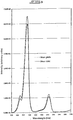
- the diamond may also exhibit 6) excellent optical properties having a UV/Visible and IR (infra-red) transparency close to the theoretical maximum for diamond and, more particularly, low or absent single substitutional nitrogen absorption at 270 nm in the UV, and low or absent C-H stretch absorption in the spectral range 2500 to 3400 cm -1 in the IR.
- excellent optical properties having a UV/Visible and IR (infra-red) transparency close to the theoretical maximum for diamond and, more particularly, low or absent single substitutional nitrogen absorption at 270 nm in the UV, and low or absent C-H stretch absorption in the spectral range 2500 to 3400 cm -1 in the IR.
- the characteristics described above will be observable in the majority volume of the layer or stone. There may be portions of the volume, generally less than 10 percent by volume, where the particular characteristic is not observable.
- the invention provides, according to another aspect, a synthetic diamond in the form of a gemstone produced from a layer of the type described above.
- the novel thick single crystal CVD diamond layer of the invention may be made by a method which forms yet another aspect of the invention. This method includes the steps of providing a diamond substrate having a surface substantially free of crystal defects, providing a source gas, dissociating the source gas and allowing homoepitaxial diamond growth on the surface of low defect level to occur in an atmosphere which contains less than 300 parts per billion nitrogen. It has been found that thick single crystal CVD diamond layers of high quality may be produced if a diamond substrate having a surface substantially free of crystal defects is used and if the homoepitaxial growth occurs in an atmosphere which contains less than 300 parts per billion molecular nitrogen.
- the invention further provides a CVD diamond produced from a single crystal CVD layer described above polished in the form of a gemstone characterised by having three orthogonal dimensions greater than 2 mm, and preferably greater than 2,5 mm, and more preferably greater than 3,0 mm, where at least one axis lies either along the ⁇ 100> crystal direction or along the principle symmetry axis of the stone.
- the diamond will be of high quality and may have one or more of the characteristics identified above.
- the single crystal CVD diamond layer of the invention has a thickness of at least 2 mm and is of high quality, and particularly is of high crystalline perfection and purity. This is evidenced by the diamond having one or more of the characteristics identified above.
- the collection distance may be determined by methods known in the art.
- the collection distances referred to in this specification were determined by the following procedure:
- the single crystal CVD diamond of the invention may, in one form of the invention, have, in the off state, a high resistivity at high applied fields and more particularly a resistivity R 1 exceeding 1 x 10 12 ⁇ cm, and preferably exceeding 2 x 10 13 ⁇ cm and more preferably exceeding 5 x 10 14 ⁇ cm, at an applied field of 50 V/ ⁇ m measured at 300 K.
- Such resistivities at such high applied fields are indicative of the purity of the diamond and the substantial absence of impurities and defects.
- Material of lower purity or crystal perfection can exhibit high resistivity at lower applied fields, e.g. ⁇ 30 V/ ⁇ m, but shows breakdown behaviour with rapidly rising leakage currents at applied fields greater than 30 V/ ⁇ m and generally by 45 V/ ⁇ m.
- the resistivity can be determined from a measurement of the leakage (dark) current by methods known in the art.
- a sample under test is prepared as a plate of uniform thickness, cleaned using standard diamond cleaning techniques in order to accept suitable contacts (evaporated, sputtered or doped diamond) to which external connections can be made to the voltage supply, and then partially or wholly encapsulated to minimise risk of flash-over. It is important to ensure that the encapsulation does not add significantly to the leakage current measured.
- Typical sample sizes are 0,01 - 0,5 mm thick by 3 x 3 mm - 50 x 50 mm laterally, but smaller or larger sizes may also be used.
- the single crystal CVD diamond of the invention may have a ⁇ product greater than 1,0 x 10 -6 cm 2 /V, preferably a ⁇ product of greater than 1,5 x 10 -6 cm 2 /V and more preferably a ⁇ product greater than 4,0 x 10 -6 cm 2 /V.
- the single crystal CVD diamond of the invention particularly in its preferred form, has a high ⁇ product which translates into a high charge collection distance.
- the CVD diamond layer of the invention may be attached to a diamond substrate (whether the substrate is synthetic, natural, or CVD diamond). Advantages of this approach include providing a greater overall thickness where the thickness limits the application, or providing support for a CVD layer whose thickness has been reduced by processing.
- the CVD diamond layer of this invention may form one layer in a multilayer device, where other diamond layers may, for example, be doped to provide electrical contact or electronic junctions to the diamond layer, or merely be present to provide support for the diamond layer.
- defects primarily means dislocations, other crystal defects and microcracks, but also includes twin boundaries, point defects, low angle boundaries and any other disruption to the crystal lattice.
- the substrate is a low birefringence type la or IIb natural, a Ib or IIa high pressure/high temperature synthetic diamond or a CVD synthesised single crystal diamond.
- the defect density is most easily characterised by optical evaluation after using a plasma or chemical etch optimised to reveal the defects (referred to as a revealing plasma etch), using for example a brief plasma etch of the type described below.
- a plasma or chemical etch optimised to reveal the defects referred to as a revealing plasma etch
- Two types of defects can be revealed:
- the preferred low density of defects is thus such that the density of surface etch features related to defects, as described above, is below 5 x 10 3 /mm 2 , and more preferably below 10 2 /mm 2 .
- the defect level at and below the substrate surface on which the CVD growth takes place may thus be minimised by careful preparation of the substrate.
- preparation includes any process applied to the material from mine recovery (in the case of natural diamond) or synthesis (in the case of synthetic material) as each stage can influence the defect density within the material at the plane which will ultimately form the substrate surface when processing to form a substrate is complete.
- Particular processing steps may include conventional diamond processes such as mechanical sawing, lapping and polishing conditions, and less conventional techniques such as laser processing or ion implantation and lift off techniques, chemical/mechanical polishing, and both liquid and plasma chemical processing techniques.
- the surface R A (arithmetic mean of the absolute deviation of surface profile measured by stylus profilometer, preferably over 0,08 mm length) should be minimised, typical values prior to any plasma etch being a few nanometers, i.e. less than 10 nm.
- One specific method of minimising the surface damage of the substrate is to include an in situ plasma etch on the surface on which the homoepitaxial diamond growth is to occur.
- this etch need not be in situ, nor immediately prior to the growth process, but the greatest benefit is achieved if it is in situ, because it avoids any risk of further physical damage or chemical contamination.
- An in situ etch is also generally most convenient when the growth process is also plasma based.
- the plasma etch can use similar conditions to the deposition or diamond growing process, but with the absence of any carbon containing source gas and generally at a slightly lower temperature to give better control of the etch rate.
- it can consist of one or more of:
- the etch consists of an oxygen etch followed by a hydrogen etch and then moving directly into synthesis by the introduction of the carbon source gas.
- the etch time/temperature is selected to enable any remaining surface damage from processing to be removed, and for any surface contaminants to be removed, but without forming a highly roughened surface and without etching extensively along extended defects (such as dislocations) which intersect the surface and thus causing deep pits.
- extended defects such as dislocations
- the hydrogen etch following the oxygen etch is less specific to crystal defects rounding off the angularities caused by the oxygen etch (which aggressively attacks such defects) and provides a smoother, better surface for subsequent growth.
- the surface or surfaces of the diamond substrate on which the CVD diamond growth occurs are preferably the ⁇ 100 ⁇ , ⁇ 110 ⁇ , ⁇ 113 ⁇ or ⁇ 111 ⁇ surfaces. Due to processing constraints, the actual sample surface orientation can differ from these orientations by up to 5°, and in some cases up to 10°, although this is less desirable as it adversely affects reproducibility.
- the impurity content of the environment in which the CVD growth takes place is properly controlled. More particularly, the diamond growth must take place in the presence of an atmosphere containing substantially no nitrogen, i.e. less than 300 parts per billion (ppb, as a molecular fraction of the total gas volume), and preferably less than 100 parts per billion.
- substantially no nitrogen i.e. less than 300 parts per billion (ppb, as a molecular fraction of the total gas volume)
- ppb parts per billion
- the source gas may be any known in the art and will contain a carbon-containing material which dissociates producing radicals or other reactive species.
- the gas mixture will also generally contain gases suitable to provide hydrogen or a halogen in atomic form.
- the dissociation of the gas source is preferably carried out using microwave energy in a reactor which may be any known in the art. However, the transfer of any impurities from the reactor should be minimised.
- a microwave system may be used to ensure that the plasma is placed away from all surfaces except the substrate surface on which diamond growth is to occur and its mount. Examples of preferred mount materials are: molybdenum, tungsten, silicon and silicon carbide. Examples of preferred reactor chamber materials are stainless steel, aluminium, copper, gold, platinum.
- a high plasma power density should be used, resulting from high microwave power (typically 3-60 kW, for substrate diameters of 50-150 mm) and high gas pressures (50-500 x 10 2 Pa, and preferably 100-450 x 10 2 Pa).
- Substrates suitable for synthesising a layer of CVD diamond of the invention may be prepared as follows:
- a high temperature/high pressure synthetic Ib diamond was grown in a high pressure press and prepared as a plate using the method described above to minimise subsurface defects.
- the final plate was 5,8 mm x 4,9 mm x 1,6 mm thick, with all faces ⁇ 100 ⁇ .
- the surface roughness at this point was less than 1 nm R A .
- This substrate (substrate 1a) was mounted, along with a second, similarly prepared, substrate (substrate 1b) on a tungsten substrate using a high temperature braze suitable for diamond. This was introduced into the reactor and an etch and growth cycle commenced as described above, and more particularly:
- the oxygen etch was at 780°C for 30 minutes and a net power of 7,8 kW.
- the hydrogen etch was at 795°C for 30 minutes.
- the atmosphere during growth contained ⁇ 100 ppb of N 2 .
- the CVD layer from substrate (2a) was 2,75 mm thick.
- This layer was processed as cut CVD synthetic in the form of a round brilliant gemstone for experimental purposes using conventional gemstone processing techniques.
- the final cut CVD synthetic stone had a weight of 0,3 ct, and had colour and quality grades equivalent to E and VS1 using the standard diamond grading system.
- a high temperature/high pressure synthetic type Ib diamond was grown in a high pressure press, and prepared using the method described in Example 1 to form a polished plate with low subsurface damage.
- the surface roughness at this stage was less than 1 nm R A .
- the substrate was mounted on a tungsten substrate using a high temperature braze suitable for diamond. This was introduced into a reactor and a growth cycle commenced as described above, and more particularly:
- the measured resistivity was in excess of 2 x 10 13 Ohm cm at an applied voltage of 50 V/ ⁇ m as measured at 300 K.
- the breakdown voltage exceeded 100 V/ ⁇ m.
Landscapes
- Chemical & Material Sciences (AREA)
- Organic Chemistry (AREA)
- Metallurgy (AREA)
- Engineering & Computer Science (AREA)
- Crystallography & Structural Chemistry (AREA)
- Materials Engineering (AREA)
- Chemical Kinetics & Catalysis (AREA)
- General Chemical & Material Sciences (AREA)
- Crystals, And After-Treatments Of Crystals (AREA)
- Chemical Vapour Deposition (AREA)
- Drying Of Semiconductors (AREA)
- Carbon And Carbon Compounds (AREA)
- Inorganic Insulating Materials (AREA)
Claims (28)
- Schicht aus Einkristall-CVD-Diamant mit einer Dicke von mehr als 2 mm, welche eines oder mehrere der folgenden Charakteristika aufweist:(i) einen hohen Ladungssammelabstand bei 300 K von mindestens 100 µm, gemessen bei einem angelegten Feld von 1 V/m;(ii) einen hohen Wert für das Produkt aus der durchschnittlichen Trägermobilität und Lebenszeit µτ, so dass es bei 300 K 1,0 x 10⁻⁶ cm2/V übersteigt;(iii) eine bei 300 K gemessene Elektronenmobilität (µe) von mehr als 2400 cm2V-1s-1;(iv) eine bei 300 K gemessene Löchermobilität (µh) von mehr als 2100 cm2V-1s-1; und(v) einen spezifischen Widerstand im Sperrzustand bei 300 K von mehr als 1012 Ωcm bei einem angelegten Feld von 50 v/µm;
und zusätzlich eines oder mehrere der folgenden Charakteristika:(a) ein Niveau an jedweder Einzelverunreinigung von nicht mehr als 1 ppm und einen Gesamtverunreinigungsgehalt von nicht mehr als 5 ppm, wobei Verunreinigung Wasserstoff und dessen isotope Formen ausschließt;(b) eine auf die Kathodolumineszenz- (CL-)Linie bei 575 nm bezogene Photolumineszenz- (PL-)Linie, gemessen bei 77 K unter Anregung mit einem 514 nm Ar-Ionenlaser (nominell 300 mW einfallender Strahl), die eine Peakhöhe < 1/25 des Raman-Peaks von Diamant bei 1332 cm-1 aufweist;(c) eine starke freie Exziton- (FE-)Emission, wobei die Stärke der durch einen 193 nm ArF-Excimer-Laser bei Raumtemperatur angeregten freien Exzitonemission derart ist, dass die Quantenausbeute für die freie Exzitonemission mindestens 10-5 beträgt;(d) ein einzelnes substitutionelles Stickstoffzentrum [N-C]° in einer Konzentration von <100 ppb in der Elektronenspinresonanz (EPR);(e) eine Spindichte von < 1 x 1017 cm-3 bei g=2,0028 in der EPR. - Schicht aus Einkristall-CVD-Diamant nach Anspruch 1, die eines oder mehrere der Charakteristika (b) bis (e) aufweist.
- Schicht aus Einkristall-CVD-Diamant nach Anspruch 1, die eines oder mehrere der Charakteristika (c) bis (e) aufweist.
- Schicht aus Einkristall-CVD-Diamant nach Anspruch 1, die eines oder mehrere der Charakteristika (d) bis (e) aufweist.
- Schicht aus Einkristall-CVD-Diamant nach Anspruch 1, die Charakteristikum (d) aufweist.
- Schicht aus Einkristall-CVD-Diamant nach einem der vorhergehenden Ansprüche mit einer Dicke von mehr als 2,5 mm.
- Schicht aus Einkristall-CVD-Diamant nach einem der vorhergehenden Ansprüche mit einer Dicke von mehr als 3 mm.
- Schicht aus Einkristall-CVD-Diamant nach einem der vorhergehenden Ansprüche, die mindestens teilweise an ein Substrat gebunden ist.
- Schicht aus Einkristall-CVD-Diamant nach einem der vorhergehenden Ansprüche, die mindestens teilweise an ein Diamantsubstrat gebunden ist.
- Diamant in Form eines Schmucksteins, der aus einer Schicht aus Einkristall-CVD-Diamant gemäß einem der Ansprüche 1 bis 7 hergestellt ist.
- Diamant nach Anspruch 10, gekennzeichnet durch drei orthogonale Dimensionen größer als 2 mm, wobei mindestens eine Achse entlang der <100>-Kristallrichtung oder entlang der Hauptsymmetrieachse des Steins liegt.
- Diamant nach Anspruch 11, gekennzeichnet durch drei orthogonale Dimensionen größer als 2,5 mm, wobei mindestens eine Achse entweder entlang der <100>-Kristallrichtung oder entlang der Hauptsymmetrieachse des Steins liegt.
- Diamant nach Anspruch 11, gekennzeichnet durch drei orthogonale Dimensionen größer als 3 mm, wobei mindestens eine Achse entweder entlang der <100>-Kristallrichtung oder entlang der Hauptsymmetrieachse des Steins liegt.
- Verfahren zum Herstellen einer Schicht aus Einkristall-CVD-Diamant nach einem der Ansprüche 1 bis 9, das die Schritte einschließt, in denen ein Diamantsubstrat mit einer Oberfläche bereitgestellt wird, die im Wesentlichen frei von Kristalldefekten ist, so dass eine offenlegende Plasmaätzung eine Dichte der defektbedingten Oberflächenätzmerkmale unter 5 x 10³/mm2 offenlegen würde, ein Quellgas bereitgestellt wird, das Quellgas dissoziiert wird und homoepitaxiales Diamantwachstum auf der Oberfläche, die im Wesentlichen frei von Kristalldefekten ist, in einer Atmosphäre zugelassen wird, die weniger als 300 ppb Stickstoff enthält.
- Verfahren nach Anspruch 14, bei dem das Substrat Diamant vom natürlichen Typ Ia oder IIb mit geringer Doppelbrechung oder ein synthetischer hoher Druck/hohe Temperatur-Diamant Ib oder IIa ist.
- Verfahren nach Anspruch 14, bei dem das Substrat CVDsynthetisierter Einkristalldiamant ist.
- Verfahren nach einem der Ansprüche 14 bis 16, bei dem die Oberfläche, auf der das Diamantwachstum stattfindet, eine Dichte der defektbedingten Oberflächenätzmerkmale unter 102/mm2 aufweist.
- Verfahren nach einem der Ansprüche 14 bis 17, bei dem die Oberfläche, auf der das Diamantwachstum stattfindet, Plasmaätzung unterzogen wird, um vor dem Diamantwachstum Oberflächenschäden der Oberfläche zu minimieren.
- Verfahren nach Anspruch 18, bei dem die Plasmaätzung eine in situ-Ätzung ist.
- Verfahren nach Anspruch 18 oder Anspruch 19, bei dem die Plasmaätzung eine Sauerstoffätzung unter Verwendung eines Ätzgases ist, das Wasserstoff und Sauerstoff enthält.
- Verfahren nach Anspruch 20, bei dem die Sauerstoffätzbedingungen ein Druck von 50 bis 450 x 102 Pa, ein Ätzgas, das einen Sauerstoffgehalt von 1 bis 4 %, einen Argongehalt bis zu 30 % und Wasserstoff als restlichen Bestandteil enthält, wobei sich alle Prozentsätze auf das Volumen beziehen, eine Substrattemperatur von 600 bis 1100°C und eine Ätzdauer von 3 bis 60 Minuten sind.
- Verfahren nach Anspruch 18 oder Anspruch 19, bei dem die Plasmaätzung eine Wasserstoffätzung ist.
- Verfahren nach Anspruch 22, bei dem die Wasserstoffätzbedingungen ein Druck von 50 bis 450 x 102 Pa, ein Ätzgas, das Wasserstoff und bis zu 30 Vol.% Argon enthält, eine Substrattemperatur von 600 bis 1100°C und eine Ätzdauer von 3 bis 60 Minuten sind.
- Verfahren nach einem der Ansprüche 18 bis 23, bei dem die Oberfläche, auf der das Diamantwachstum stattfindet, sowohl einer Sauerstoffätzung als auch einer Wasserstoffätzung unterzogen wird, um vor dem Diamantwachstum Schäden an der Oberfläche zu minimieren.
- Verfahren nach Anspruch 24, bei dem der Sauerstoffätzung eine Wasserstoffätzung folgt.
- Verfahren nach einem der Ansprüche 18 bis 25, bei dem die Oberfläche RA der Oberfläche, auf der das Diamantwachstum stattfindet, kleiner als 10 Nanometer ist, bevor diese Oberfläche der Plasmaätzung unterzogen wird.
- Verfahren nach einem der Ansprüche 14 bis 26, bei dem die Oberfläche, auf der das Diamantwachstum stattfindet, im Wesentlichen eine {100}-, {110}-, {113}- oder {111}-Oberfläche ist.
- Verfahren nach einem der Ansprüche 14 bis 27, bei dem die Dissoziation des Quellgases unter Verwendung von Mikrowellenenergie stattfindet.
Applications Claiming Priority (3)
| Application Number | Priority Date | Filing Date | Title |
|---|---|---|---|
| GB0014690A GB0014690D0 (en) | 2000-06-15 | 2000-06-15 | Diamond |
| GB0106929A GB0106929D0 (en) | 2001-03-20 | 2001-03-20 | Diamond |
| EP01943715A EP1290251B8 (de) | 2000-06-15 | 2001-06-14 | Dicke einkristalline diamantschicht, verfahren zur herstellung der schicht und edelsteine hergestellt durch bearbeitung der schicht |
Related Parent Applications (1)
| Application Number | Title | Priority Date | Filing Date |
|---|---|---|---|
| EP01943715A Division EP1290251B8 (de) | 2000-06-15 | 2001-06-14 | Dicke einkristalline diamantschicht, verfahren zur herstellung der schicht und edelsteine hergestellt durch bearbeitung der schicht |
Publications (3)
| Publication Number | Publication Date |
|---|---|
| EP1632590A2 EP1632590A2 (de) | 2006-03-08 |
| EP1632590A3 EP1632590A3 (de) | 2006-05-24 |
| EP1632590B1 true EP1632590B1 (de) | 2017-01-11 |
Family
ID=26244496
Family Applications (2)
| Application Number | Title | Priority Date | Filing Date |
|---|---|---|---|
| EP01943715A Expired - Lifetime EP1290251B8 (de) | 2000-06-15 | 2001-06-14 | Dicke einkristalline diamantschicht, verfahren zur herstellung der schicht und edelsteine hergestellt durch bearbeitung der schicht |
| EP05077372.0A Expired - Lifetime EP1632590B1 (de) | 2000-06-15 | 2001-06-14 | Dicke einkristalline Diamantschicht, Verfahren zur Herstellung der Schicht und Edelsteine hergestellt durch Bearbeitung der Schicht |
Family Applications Before (1)
| Application Number | Title | Priority Date | Filing Date |
|---|---|---|---|
| EP01943715A Expired - Lifetime EP1290251B8 (de) | 2000-06-15 | 2001-06-14 | Dicke einkristalline diamantschicht, verfahren zur herstellung der schicht und edelsteine hergestellt durch bearbeitung der schicht |
Country Status (16)
| Country | Link |
|---|---|
| US (3) | US7128974B2 (de) |
| EP (2) | EP1290251B8 (de) |
| JP (1) | JP4469552B2 (de) |
| KR (1) | KR100839707B1 (de) |
| CN (1) | CN1210445C (de) |
| AT (1) | ATE311486T1 (de) |
| AU (2) | AU6624601A (de) |
| CA (1) | CA2412855C (de) |
| CZ (1) | CZ302229B6 (de) |
| DE (1) | DE60115435T2 (de) |
| ES (1) | ES2252244T3 (de) |
| GB (1) | GB2379451B (de) |
| IL (2) | IL153381A0 (de) |
| RU (1) | RU2287028C2 (de) |
| TW (1) | TWI250231B (de) |
| WO (1) | WO2001096634A1 (de) |
Families Citing this family (76)
| Publication number | Priority date | Publication date | Assignee | Title |
|---|---|---|---|---|
| US8591856B2 (en) | 1998-05-15 | 2013-11-26 | SCIO Diamond Technology Corporation | Single crystal diamond electrochemical electrode |
| US6858080B2 (en) | 1998-05-15 | 2005-02-22 | Apollo Diamond, Inc. | Tunable CVD diamond structures |
| US6582513B1 (en) | 1998-05-15 | 2003-06-24 | Apollo Diamond, Inc. | System and method for producing synthetic diamond |
| DE60135653D1 (de) * | 2000-06-15 | 2008-10-16 | Element Six Pty Ltd | Einkristalldiamant hergestellt durch cvd |
| AU2001281404B2 (en) | 2001-08-08 | 2008-07-03 | Apollo Diamond, Inc. | System and method for producing synthetic diamond |
| DE10153310A1 (de) * | 2001-10-29 | 2003-05-22 | Infineon Technologies Ag | Photolithographisches Strukturierungsverfahren mit einer durch ein plasmaunterstützes Abscheideeverfahren hergestellten Kohlenstoff-Hartmaskenschicht diamantartiger Härte |
| GB0130004D0 (en) * | 2001-12-14 | 2002-02-06 | Diamanx Products Ltd | Coloured diamond |
| GB0130005D0 (en) * | 2001-12-14 | 2002-02-06 | Diamanx Products Ltd | Boron doped diamond |
| GB0220772D0 (en) * | 2002-09-06 | 2002-10-16 | Diamanx Products Ltd | Coloured diamond |
| RU2328563C2 (ru) * | 2002-09-06 | 2008-07-10 | Элемент Сикс Лимитед | Цветные алмазы |
| GB0220767D0 (en) * | 2002-09-06 | 2002-10-16 | Diamanx Products Ltd | Diamond radiation detector |
| GB0221949D0 (en) * | 2002-09-20 | 2002-10-30 | Diamanx Products Ltd | Single crystal diamond |
| GB0227261D0 (en) * | 2002-11-21 | 2002-12-31 | Element Six Ltd | Optical quality diamond material |
| FR2849867B1 (fr) | 2003-01-10 | 2005-03-25 | Centre Nat Rech Scient | Croissance diamant a grande vitesse par plasma micro-onde en regime pulse. |
| GB0303860D0 (en) * | 2003-02-19 | 2003-03-26 | Element Six Ltd | CVD diamond in wear applications |
| CA2548449C (en) | 2003-12-12 | 2014-06-03 | Element Six Limited | Method of incorporating a mark in cvd diamond |
| US7481879B2 (en) | 2004-01-16 | 2009-01-27 | Sumitomo Electric Industries, Ltd. | Diamond single crystal substrate manufacturing method and diamond single crystal substrate |
| JP4697514B2 (ja) * | 2004-01-16 | 2011-06-08 | 住友電気工業株式会社 | ダイヤモンド単結晶基板の製造方法およびダイヤモンド単結晶基板 |
| US7918293B1 (en) | 2005-03-09 | 2011-04-05 | Us Synthetic Corporation | Method and system for perceiving a boundary between a first region and a second region of a superabrasive volume |
| JP5002982B2 (ja) * | 2005-04-15 | 2012-08-15 | 住友電気工業株式会社 | 単結晶ダイヤモンドの製造方法 |
| GB0508889D0 (en) * | 2005-04-29 | 2005-06-08 | Element Six Ltd | Diamond transistor and method of manufacture thereof |
| KR101307032B1 (ko) * | 2005-06-22 | 2013-09-11 | 엘리멘트 식스 리미티드 | 고등급의 색을 갖는 다이아몬드 층 |
| US9133566B2 (en) | 2005-12-09 | 2015-09-15 | Element Six Technologies Limited | High crystalline quality synthetic diamond |
| GB0622695D0 (en) | 2006-11-14 | 2006-12-27 | Element Six Ltd | Robust radiation detector comprising diamond |
| JP5341774B2 (ja) | 2007-01-22 | 2013-11-13 | エレメント シックス リミテッド | ダイヤモンド表面のプラズマエッチング |
| JP5514552B2 (ja) * | 2007-01-29 | 2014-06-04 | カーネギー インスチチューション オブ ワシントン | 単結晶cvdダイヤモンドの新規なレーザー用途 |
| JP5223201B2 (ja) * | 2007-01-29 | 2013-06-26 | 日本電気株式会社 | 電界効果トランジスタ |
| JP5504565B2 (ja) * | 2008-02-07 | 2014-05-28 | 独立行政法人物質・材料研究機構 | ダイヤモンド紫外線センサー素子とその製造方法、並びに紫外線センサー装置 |
| WO2009114130A2 (en) * | 2008-03-13 | 2009-09-17 | Michigan State University | Process and apparatus for diamond synthesis |
| US20090260396A1 (en) * | 2008-04-16 | 2009-10-22 | Eitan Broukman | Methods for processing ornamental diamonds and corresponding ornamental diamonds |
| US8342164B2 (en) * | 2008-05-09 | 2013-01-01 | SCIO Diamond Technology Corporation | Gemstone production from CVD diamond plate |
| GB0813491D0 (en) * | 2008-07-23 | 2008-08-27 | Element Six Ltd | Diamond Material |
| GB0813490D0 (en) | 2008-07-23 | 2008-08-27 | Element Six Ltd | Solid state material |
| GB0819001D0 (en) | 2008-10-16 | 2008-11-26 | Diamond Detectors Ltd | Contacts on diamond |
| US9017632B2 (en) | 2009-06-26 | 2015-04-28 | Element Six Technologies Limited | Diamond material |
| JP5874932B2 (ja) * | 2009-06-26 | 2016-03-02 | エレメント シックス リミテッド | ダイヤモンド材料の処理方法及び得られた製品 |
| KR101130049B1 (ko) * | 2009-09-08 | 2012-03-28 | 김일천 | 다이아몬드상 카본 박막 코팅 피스톤 및 그 제조방법 |
| GB201000768D0 (en) * | 2010-01-18 | 2010-03-03 | Element Six Ltd | CVD single crystal diamond material |
| US9017633B2 (en) | 2010-01-18 | 2015-04-28 | Element Six Technologies Limited | CVD single crystal diamond material |
| JP2013532109A (ja) * | 2010-05-17 | 2013-08-15 | カーネギー インスチチューション オブ ワシントン | 大形、高純度、単結晶のcvdダイヤモンドの生成 |
| GB201013112D0 (en) | 2010-08-04 | 2010-09-22 | Element Six Ltd | A diamond optical element |
| US9277792B2 (en) * | 2010-08-24 | 2016-03-08 | Board Of Trustees Of Michigan State University | Multicolored single crystal diamond gemstones and methods for forming the same |
| GB201015260D0 (en) | 2010-09-14 | 2010-10-27 | Element Six Ltd | A microfluidic cell and a spin resonance device for use therewith |
| GB201021985D0 (en) | 2010-12-24 | 2011-02-02 | Element Six Ltd | Dislocation engineering in single crystal synthetic diamond material |
| GB201104579D0 (en) * | 2011-03-18 | 2011-05-04 | Element Six Ltd | Diamond based electrochemical sensors |
| GB201107730D0 (en) | 2011-05-10 | 2011-06-22 | Element Six Ltd | Diamond sensors, detectors and quantum devices |
| US20130026492A1 (en) * | 2011-07-30 | 2013-01-31 | Akhan Technologies Inc. | Diamond Semiconductor System and Method |
| GB201121642D0 (en) | 2011-12-16 | 2012-01-25 | Element Six Ltd | Single crtstal cvd synthetic diamond material |
| US8969833B1 (en) | 2011-12-16 | 2015-03-03 | Us Synthetic Corporation | Method and system for perceiving a boundary between a first region and a second region of a superabrasive volume |
| US8933462B2 (en) * | 2011-12-21 | 2015-01-13 | Akhan Semiconductor, Inc. | Method of fabricating diamond semiconductor and diamond semiconductor formed according to the method |
| US20130175546A1 (en) * | 2012-01-06 | 2013-07-11 | Akhan Technologies, Inc. | Diamond Semiconductor System and Method |
| GB201216697D0 (en) * | 2012-09-19 | 2012-10-31 | Element Six Ltd | Single crystal chemical vapour deposited synthetic diamond materials having uniform colour |
| CN103305807B (zh) * | 2013-05-07 | 2015-06-24 | 大连理工大学 | 一种制备氮掺杂纳米金刚石的方法及其电催化应用 |
| GB201320304D0 (en) * | 2013-11-18 | 2014-01-01 | Element Six Ltd | Methods of fabricating synthetic diamond materials using microwave plasma actived chemical vapour deposition techniques and products obtained using said |
| CN106574393B (zh) | 2014-07-22 | 2019-10-08 | 住友电气工业株式会社 | 单晶金刚石及其制造方法、包含单晶金刚石的工具和包含单晶金刚石的部件 |
| CN106661758A (zh) | 2014-08-08 | 2017-05-10 | 住友电气工业株式会社 | 制造金刚石的方法、金刚石、金刚石复合基板、金刚石接合基板和工具 |
| SG10201505413VA (en) * | 2015-01-14 | 2016-08-30 | Iia Technologies Pte Ltd | Electronic device grade single crystal diamonds and method of producing the same |
| DK3045570T3 (da) | 2015-01-14 | 2019-08-26 | Iia Tech Pte Ltd | Enkeltkrystaldiamanter af en kvalitet til elektroniske indretninger og fremgangsmåde til fremstilling deraf |
| CN104911702B (zh) * | 2015-04-29 | 2017-07-28 | 西安交通大学 | 基于自组装工艺的高质量单晶金刚石生长方法 |
| GB201516814D0 (en) | 2015-09-23 | 2015-11-04 | Element Six Technologies Ltd | Method of fabricating a plurality of single crystal CVD synthetic diamonds |
| SG11201805526PA (en) | 2016-01-22 | 2018-08-30 | Sumitomo Electric Industries | Single-crystal diamond, method for manufacturing single-crystal diamond, and chemical vapor deposition device used in same |
| GB201610053D0 (en) * | 2016-06-09 | 2016-07-27 | Element Six Tech Ltd | Synthetic diamond heat spreaders |
| US9922823B1 (en) * | 2016-09-07 | 2018-03-20 | Euclid Techlabs, Llc | CVD reactor and method for nanometric delta doping of diamond |
| GB201620413D0 (en) | 2016-12-01 | 2017-01-18 | Element Six Tech Ltd | Single crystal synthetic diamond material via chemical vapour deposition |
| ES2724214B2 (es) | 2018-03-01 | 2020-01-15 | Business Res And Diamonds S L | Procedimiento para la obtencion de diamantes sinteticos a partir de la sacarosa y equipo para llevar a cabo dicho procedimiento |
| GB201904435D0 (en) | 2019-03-29 | 2019-05-15 | Element Six Tech Ltd | Single crystal synthetic diamond material |
| CN109911894A (zh) * | 2019-03-31 | 2019-06-21 | 河北地质大学 | 微波等离子体化学气相沉积法生长多晶金刚石片的方法 |
| GB202003310D0 (en) * | 2020-03-06 | 2020-04-22 | Element Six Tech Ltd | Method for forming diamond product |
| US11185139B1 (en) | 2021-03-04 | 2021-11-30 | Oujie Kevin Tong | Coating compositions and method for jewelries |
| GB2614521A (en) | 2021-10-19 | 2023-07-12 | Element Six Tech Ltd | CVD single crystal diamond |
| GB2614068B (en) | 2021-12-21 | 2024-05-22 | Element Six Tech Ltd | Sensor device |
| GB2614530B (en) | 2021-12-23 | 2024-12-11 | Element Six Tech Ltd | Diamond sensor |
| CN114941173B (zh) * | 2022-05-26 | 2023-10-10 | 曲阜师范大学 | 一种高相干金刚石氮空穴及金刚石压砧的制备与应用 |
| GB202219497D0 (en) | 2022-12-22 | 2023-02-08 | Element Six Tech Ltd | Single crystal diamond |
| GB202305972D0 (en) | 2023-04-24 | 2023-06-07 | Element Six Tech Ltd | Method of manufacturing single crystal diamonds |
| GB2630986A (en) | 2023-06-16 | 2024-12-18 | Element Six Tech Ltd | Single crystal diamond product |
Family Cites Families (40)
| Publication number | Priority date | Publication date | Assignee | Title |
|---|---|---|---|---|
| US246762A (en) * | 1881-09-06 | Preserving wood | ||
| US248810A (en) * | 1881-10-25 | Ttorney | ||
| US2317176A (en) * | 1941-05-14 | 1943-04-20 | Marie A Byrd | Container bag and outer garment |
| JP2571795B2 (ja) | 1987-11-17 | 1997-01-16 | 住友電気工業株式会社 | 紫色ダイヤモンドおよびその製造方法 |
| JP2691219B2 (ja) | 1988-10-17 | 1997-12-17 | 並木精密宝石株式会社 | ダイヤモンドの合成法 |
| JP2730144B2 (ja) * | 1989-03-07 | 1998-03-25 | 住友電気工業株式会社 | 単結晶ダイヤモンド層形成法 |
| JP2730145B2 (ja) * | 1989-03-07 | 1998-03-25 | 住友電気工業株式会社 | 単結晶ダイヤモンド層の形成法 |
| US6007916A (en) * | 1989-04-06 | 1999-12-28 | Sumitomo Electric Industries, Ltd. | Synthetic single crystal diamond for wiring drawing dies and process for producing the same |
| US5127983A (en) * | 1989-05-22 | 1992-07-07 | Sumitomo Electric Industries, Ltd. | Method of producing single crystal of high-pressure phase material |
| AU634601B2 (en) * | 1989-12-11 | 1993-02-25 | General Electric Company | Single-crystal diamond of very high thermal conductivity |
| US5360479A (en) * | 1990-07-02 | 1994-11-01 | General Electric Company | Isotopically pure single crystal epitaxial diamond films and their preparation |
| US5704976A (en) * | 1990-07-06 | 1998-01-06 | The United States Of America As Represented By The Secretary Of The Navy | High temperature, high rate, epitaxial synthesis of diamond in a laminar plasma |
| CA2049673A1 (en) * | 1990-11-26 | 1992-05-27 | James F. Fleischer | Cvd diamond by alternating chemical reactions |
| JPH04305096A (ja) * | 1991-04-01 | 1992-10-28 | Sumitomo Electric Ind Ltd | 高品質気相合成ダイヤモンドの低温形成法 |
| US5614019A (en) * | 1992-06-08 | 1997-03-25 | Air Products And Chemicals, Inc. | Method for the growth of industrial crystals |
| US5443032A (en) | 1992-06-08 | 1995-08-22 | Air Products And Chemicals, Inc. | Method for the manufacture of large single crystals |
| EP0582397A3 (de) * | 1992-08-05 | 1995-01-25 | Crystallume | CVD-Diamant-Material für einen Strahlungsdetektor und Herstellungsverfahren. |
| US5334283A (en) * | 1992-08-31 | 1994-08-02 | The University Of North Carolina At Chapel Hill | Process for selectively etching diamond |
| US5474021A (en) | 1992-09-24 | 1995-12-12 | Sumitomo Electric Industries, Ltd. | Epitaxial growth of diamond from vapor phase |
| JPH06107494A (ja) | 1992-09-24 | 1994-04-19 | Sumitomo Electric Ind Ltd | ダイヤモンドの気相成長法 |
| JP3314444B2 (ja) | 1993-03-15 | 2002-08-12 | 住友電気工業株式会社 | 赤色ダイヤモンドおよび桃色ダイヤモンド |
| CA2127832C (en) * | 1993-07-20 | 2001-02-20 | Grant Lu | Cvd diamond radiation detector |
| US5390409A (en) * | 1993-08-27 | 1995-02-21 | General Electric Co. | Methods of manufacturing of generator stator frames |
| CN1087132A (zh) * | 1993-09-03 | 1994-05-25 | 国家建筑材料工业局人工晶体研究所 | 用于拉丝模的金刚石膜及其制法 |
| JP3484749B2 (ja) | 1994-04-04 | 2004-01-06 | 住友電気工業株式会社 | ダイヤモンドの合成法 |
| EP0688026A1 (de) | 1994-06-17 | 1995-12-20 | General Electric Company | Widerstand auf einem Substrat aus Diamant |
| US5587210A (en) * | 1994-06-28 | 1996-12-24 | The United States Of America As Represented By The Secretary Of The Navy | Growing and releasing diamonds |
| JP4291886B2 (ja) | 1994-12-05 | 2009-07-08 | 住友電気工業株式会社 | 低欠陥ダイヤモンド単結晶及びその合成方法 |
| JP3675577B2 (ja) * | 1995-07-05 | 2005-07-27 | 日本特殊陶業株式会社 | ダイヤモンド被覆物品の製造方法 |
| GB9616043D0 (en) * | 1996-07-31 | 1996-09-11 | De Beers Ind Diamond | Diamond |
| JP4032482B2 (ja) | 1997-04-18 | 2008-01-16 | 住友電気工業株式会社 | 単結晶ダイヤモンドの製造方法 |
| JPH11107596A (ja) | 1997-10-07 | 1999-04-20 | Osamu Ito | 地震揺れを検知して作動する自動解錠装置 |
| JP3125046B2 (ja) * | 1997-11-21 | 2001-01-15 | 工業技術院長 | ダイヤモンド単結晶薄膜製造方法 |
| US6582513B1 (en) * | 1998-05-15 | 2003-06-24 | Apollo Diamond, Inc. | System and method for producing synthetic diamond |
| DE60135653D1 (de) * | 2000-06-15 | 2008-10-16 | Element Six Pty Ltd | Einkristalldiamant hergestellt durch cvd |
| GB0130005D0 (en) | 2001-12-14 | 2002-02-06 | Diamanx Products Ltd | Boron doped diamond |
| GB0130004D0 (en) | 2001-12-14 | 2002-02-06 | Diamanx Products Ltd | Coloured diamond |
| RU2328563C2 (ru) | 2002-09-06 | 2008-07-10 | Элемент Сикс Лимитед | Цветные алмазы |
| GB0221949D0 (en) | 2002-09-20 | 2002-10-30 | Diamanx Products Ltd | Single crystal diamond |
| GB0227261D0 (en) | 2002-11-21 | 2002-12-31 | Element Six Ltd | Optical quality diamond material |
-
2001
- 2001-06-14 JP JP2002510742A patent/JP4469552B2/ja not_active Expired - Lifetime
- 2001-06-14 AU AU6624601A patent/AU6624601A/xx active Pending
- 2001-06-14 AT AT01943715T patent/ATE311486T1/de not_active IP Right Cessation
- 2001-06-14 AU AU2001266246A patent/AU2001266246B2/en not_active Ceased
- 2001-06-14 DE DE60115435T patent/DE60115435T2/de not_active Expired - Lifetime
- 2001-06-14 RU RU2002135628/15A patent/RU2287028C2/ru active
- 2001-06-14 CN CNB018127193A patent/CN1210445C/zh not_active Expired - Lifetime
- 2001-06-14 GB GB0300200A patent/GB2379451B/en not_active Expired - Lifetime
- 2001-06-14 IL IL15338101A patent/IL153381A0/xx active IP Right Grant
- 2001-06-14 EP EP01943715A patent/EP1290251B8/de not_active Expired - Lifetime
- 2001-06-14 KR KR1020027017121A patent/KR100839707B1/ko not_active Expired - Lifetime
- 2001-06-14 WO PCT/IB2001/001040 patent/WO2001096634A1/en not_active Ceased
- 2001-06-14 CZ CZ20024228A patent/CZ302229B6/cs not_active IP Right Cessation
- 2001-06-14 EP EP05077372.0A patent/EP1632590B1/de not_active Expired - Lifetime
- 2001-06-14 ES ES01943715T patent/ES2252244T3/es not_active Expired - Lifetime
- 2001-06-14 CA CA002412855A patent/CA2412855C/en not_active Expired - Lifetime
- 2001-11-06 TW TW090127518A patent/TWI250231B/zh not_active IP Right Cessation
-
2002
- 2002-12-11 IL IL153381A patent/IL153381A/en unknown
-
2003
- 2003-12-19 US US10/739,014 patent/US7128974B2/en not_active Expired - Lifetime
-
2006
- 2006-07-14 US US11/486,421 patent/US20070148079A1/en not_active Abandoned
-
2007
- 2007-03-05 US US11/681,840 patent/US7887628B2/en not_active Expired - Fee Related
Also Published As
Similar Documents
| Publication | Publication Date | Title |
|---|---|---|
| EP1632590B1 (de) | Dicke einkristalline Diamantschicht, Verfahren zur Herstellung der Schicht und Edelsteine hergestellt durch Bearbeitung der Schicht | |
| EP1292726B8 (de) | Einkristalldiamant hergestellt durch cvd | |
| AU2001266246A1 (en) | Thick single crystal diamond layer method for making it and gemstones produced from the layer | |
| AU2001274368A1 (en) | Single crystal diamond prepared by CVD | |
| EP1463849B1 (de) | Bordotierte diamant und verfahren zu ihrer herstellung | |
| ZA200210138B (en) | Thick single crystal diamond layer method for making it and gemstones produced from the layer. | |
| ZA200210140B (en) | Single crystal diamond prepared by CVD. |
Legal Events
| Date | Code | Title | Description |
|---|---|---|---|
| PUAI | Public reference made under article 153(3) epc to a published international application that has entered the european phase |
Free format text: ORIGINAL CODE: 0009012 |
|
| AC | Divisional application: reference to earlier application |
Ref document number: 1290251 Country of ref document: EP Kind code of ref document: P |
|
| AK | Designated contracting states |
Kind code of ref document: A2 Designated state(s): AT BE CH CY DE DK ES FI FR GB GR IE IT LI LU MC NL PT SE TR |
|
| PUAL | Search report despatched |
Free format text: ORIGINAL CODE: 0009013 |
|
| RIN1 | Information on inventor provided before grant (corrected) |
Inventor name: SCARSBROOK, GEOFFREY ALAN Inventor name: TWITCHEN, DANIEL JAMES Inventor name: COLLINS, JOHN LLOYD Inventor name: COOPER, ANDREW MICHAEL Inventor name: WHITEHEAD, ANDREW JOHN Inventor name: MARTINEAU, PHILIP MAURICE Inventor name: DORN, BAERBEL SUSANNE CHARLOTTE |
|
| AK | Designated contracting states |
Kind code of ref document: A3 Designated state(s): AT BE CH CY DE DK ES FI FR GB GR IE IT LI LU MC NL PT SE TR |
|
| 17P | Request for examination filed |
Effective date: 20061110 |
|
| AKX | Designation fees paid |
Designated state(s): AT BE CH CY DE DK ES FI FR GB GR IE IT LI LU MC NL PT SE TR |
|
| 17Q | First examination report despatched |
Effective date: 20070222 |
|
| APBK | Appeal reference recorded |
Free format text: ORIGINAL CODE: EPIDOSNREFNE |
|
| APBN | Date of receipt of notice of appeal recorded |
Free format text: ORIGINAL CODE: EPIDOSNNOA2E |
|
| APBR | Date of receipt of statement of grounds of appeal recorded |
Free format text: ORIGINAL CODE: EPIDOSNNOA3E |
|
| APAF | Appeal reference modified |
Free format text: ORIGINAL CODE: EPIDOSCREFNE |
|
| RAP1 | Party data changed (applicant data changed or rights of an application transferred) |
Owner name: ELEMENT SIX TECHNOLOGIES LIMITED |
|
| APBT | Appeal procedure closed |
Free format text: ORIGINAL CODE: EPIDOSNNOA9E |
|
| GRAP | Despatch of communication of intention to grant a patent |
Free format text: ORIGINAL CODE: EPIDOSNIGR1 |
|
| RIC1 | Information provided on ipc code assigned before grant |
Ipc: A44C 17/00 20060101ALI20160502BHEP Ipc: C30B 25/02 20060101AFI20160502BHEP Ipc: B01J 3/06 20060101ALI20160502BHEP Ipc: C30B 29/04 20060101ALI20160502BHEP Ipc: C23C 16/27 20060101ALI20160502BHEP Ipc: C30B 25/10 20060101ALI20160502BHEP Ipc: C30B 33/00 20060101ALI20160502BHEP Ipc: C30B 25/20 20060101ALI20160502BHEP |
|
| INTG | Intention to grant announced |
Effective date: 20160525 |
|
| GRAS | Grant fee paid |
Free format text: ORIGINAL CODE: EPIDOSNIGR3 |
|
| STAA | Information on the status of an ep patent application or granted ep patent |
Free format text: STATUS: GRANT OF PATENT IS INTENDED |
|
| GRAA | (expected) grant |
Free format text: ORIGINAL CODE: 0009210 |
|
| STAA | Information on the status of an ep patent application or granted ep patent |
Free format text: STATUS: THE PATENT HAS BEEN GRANTED |
|
| AC | Divisional application: reference to earlier application |
Ref document number: 1290251 Country of ref document: EP Kind code of ref document: P |
|
| AK | Designated contracting states |
Kind code of ref document: B1 Designated state(s): AT BE CH CY DE DK ES FI FR GB GR IE IT LI LU MC NL PT SE TR |
|
| REG | Reference to a national code |
Ref country code: GB Ref legal event code: FG4D |
|
| REG | Reference to a national code |
Ref country code: CH Ref legal event code: EP Ref country code: CH Ref legal event code: NV Representative=s name: E. BLUM AND CO. AG PATENT- UND MARKENANWAELTE , CH |
|
| REG | Reference to a national code |
Ref country code: AT Ref legal event code: REF Ref document number: 861367 Country of ref document: AT Kind code of ref document: T Effective date: 20170115 |
|
| REG | Reference to a national code |
Ref country code: IE Ref legal event code: FG4D |
|
| REG | Reference to a national code |
Ref country code: DE Ref legal event code: R096 Ref document number: 60150283 Country of ref document: DE |
|
| REG | Reference to a national code |
Ref country code: NL Ref legal event code: FP |
|
| REG | Reference to a national code |
Ref country code: AT Ref legal event code: MK05 Ref document number: 861367 Country of ref document: AT Kind code of ref document: T Effective date: 20170111 |
|
| REG | Reference to a national code |
Ref country code: FR Ref legal event code: PLFP Year of fee payment: 17 |
|
| PG25 | Lapsed in a contracting state [announced via postgrant information from national office to epo] |
Ref country code: FI Free format text: LAPSE BECAUSE OF FAILURE TO SUBMIT A TRANSLATION OF THE DESCRIPTION OR TO PAY THE FEE WITHIN THE PRESCRIBED TIME-LIMIT Effective date: 20170111 Ref country code: GR Free format text: LAPSE BECAUSE OF FAILURE TO SUBMIT A TRANSLATION OF THE DESCRIPTION OR TO PAY THE FEE WITHIN THE PRESCRIBED TIME-LIMIT Effective date: 20170412 |
|
| PG25 | Lapsed in a contracting state [announced via postgrant information from national office to epo] |
Ref country code: SE Free format text: LAPSE BECAUSE OF FAILURE TO SUBMIT A TRANSLATION OF THE DESCRIPTION OR TO PAY THE FEE WITHIN THE PRESCRIBED TIME-LIMIT Effective date: 20170111 Ref country code: ES Free format text: LAPSE BECAUSE OF FAILURE TO SUBMIT A TRANSLATION OF THE DESCRIPTION OR TO PAY THE FEE WITHIN THE PRESCRIBED TIME-LIMIT Effective date: 20170111 Ref country code: PT Free format text: LAPSE BECAUSE OF FAILURE TO SUBMIT A TRANSLATION OF THE DESCRIPTION OR TO PAY THE FEE WITHIN THE PRESCRIBED TIME-LIMIT Effective date: 20170511 Ref country code: AT Free format text: LAPSE BECAUSE OF FAILURE TO SUBMIT A TRANSLATION OF THE DESCRIPTION OR TO PAY THE FEE WITHIN THE PRESCRIBED TIME-LIMIT Effective date: 20170111 |
|
| REG | Reference to a national code |
Ref country code: DE Ref legal event code: R097 Ref document number: 60150283 Country of ref document: DE |
|
| PLBE | No opposition filed within time limit |
Free format text: ORIGINAL CODE: 0009261 |
|
| STAA | Information on the status of an ep patent application or granted ep patent |
Free format text: STATUS: NO OPPOSITION FILED WITHIN TIME LIMIT |
|
| PG25 | Lapsed in a contracting state [announced via postgrant information from national office to epo] |
Ref country code: DK Free format text: LAPSE BECAUSE OF FAILURE TO SUBMIT A TRANSLATION OF THE DESCRIPTION OR TO PAY THE FEE WITHIN THE PRESCRIBED TIME-LIMIT Effective date: 20170111 |
|
| 26N | No opposition filed |
Effective date: 20171012 |
|
| PG25 | Lapsed in a contracting state [announced via postgrant information from national office to epo] |
Ref country code: MC Free format text: LAPSE BECAUSE OF FAILURE TO SUBMIT A TRANSLATION OF THE DESCRIPTION OR TO PAY THE FEE WITHIN THE PRESCRIBED TIME-LIMIT Effective date: 20170111 |
|
| REG | Reference to a national code |
Ref country code: IE Ref legal event code: MM4A |
|
| PG25 | Lapsed in a contracting state [announced via postgrant information from national office to epo] |
Ref country code: LU Free format text: LAPSE BECAUSE OF NON-PAYMENT OF DUE FEES Effective date: 20170614 Ref country code: IE Free format text: LAPSE BECAUSE OF NON-PAYMENT OF DUE FEES Effective date: 20170614 |
|
| REG | Reference to a national code |
Ref country code: FR Ref legal event code: PLFP Year of fee payment: 18 |
|
| PG25 | Lapsed in a contracting state [announced via postgrant information from national office to epo] |
Ref country code: CY Free format text: LAPSE BECAUSE OF NON-PAYMENT OF DUE FEES Effective date: 20170111 |
|
| PG25 | Lapsed in a contracting state [announced via postgrant information from national office to epo] |
Ref country code: TR Free format text: LAPSE BECAUSE OF FAILURE TO SUBMIT A TRANSLATION OF THE DESCRIPTION OR TO PAY THE FEE WITHIN THE PRESCRIBED TIME-LIMIT Effective date: 20170111 |
|
| PGFP | Annual fee paid to national office [announced via postgrant information from national office to epo] |
Ref country code: DE Payment date: 20200618 Year of fee payment: 20 Ref country code: FR Payment date: 20200619 Year of fee payment: 20 Ref country code: CH Payment date: 20200618 Year of fee payment: 20 |
|
| PGFP | Annual fee paid to national office [announced via postgrant information from national office to epo] |
Ref country code: GB Payment date: 20200625 Year of fee payment: 20 Ref country code: NL Payment date: 20200625 Year of fee payment: 20 Ref country code: IT Payment date: 20200623 Year of fee payment: 20 Ref country code: BE Payment date: 20200625 Year of fee payment: 20 |
|
| REG | Reference to a national code |
Ref country code: DE Ref legal event code: R071 Ref document number: 60150283 Country of ref document: DE |
|
| REG | Reference to a national code |
Ref country code: NL Ref legal event code: MK Effective date: 20210613 |
|
| REG | Reference to a national code |
Ref country code: CH Ref legal event code: PL |
|
| REG | Reference to a national code |
Ref country code: GB Ref legal event code: PE20 Expiry date: 20210613 |
|
| REG | Reference to a national code |
Ref country code: BE Ref legal event code: MK Effective date: 20210614 |
|
| PG25 | Lapsed in a contracting state [announced via postgrant information from national office to epo] |
Ref country code: GB Free format text: LAPSE BECAUSE OF EXPIRATION OF PROTECTION Effective date: 20210613 |