EP1629063B2 - Organic electroluminescent devices and metal complex compounds - Google Patents
Organic electroluminescent devices and metal complex compounds Download PDFInfo
- Publication number
- EP1629063B2 EP1629063B2 EP04735658.9A EP04735658A EP1629063B2 EP 1629063 B2 EP1629063 B2 EP 1629063B2 EP 04735658 A EP04735658 A EP 04735658A EP 1629063 B2 EP1629063 B2 EP 1629063B2
- Authority
- EP
- European Patent Office
- Prior art keywords
- group
- carbon atoms
- compound
- derivatives
- layer
- Prior art date
- Legal status (The legal status is an assumption and is not a legal conclusion. Google has not performed a legal analysis and makes no representation as to the accuracy of the status listed.)
- Expired - Lifetime
Links
- 0 I*1(c2ccccc2C2C=CC=C(C3)*12)C(CCC=C1)=C1c1nc3ccc1 Chemical compound I*1(c2ccccc2C2C=CC=C(C3)*12)C(CCC=C1)=C1c1nc3ccc1 0.000 description 7
Classifications
-
- C—CHEMISTRY; METALLURGY
- C07—ORGANIC CHEMISTRY
- C07F—ACYCLIC, CARBOCYCLIC OR HETEROCYCLIC COMPOUNDS CONTAINING ELEMENTS OTHER THAN CARBON, HYDROGEN, HALOGEN, OXYGEN, NITROGEN, SULFUR, SELENIUM OR TELLURIUM
- C07F15/00—Compounds containing elements of Groups 8, 9, 10 or 18 of the Periodic Table
- C07F15/0006—Compounds containing elements of Groups 8, 9, 10 or 18 of the Periodic Table compounds of the platinum group
- C07F15/0086—Platinum compounds
- C07F15/0093—Platinum compounds without a metal-carbon linkage
-
- C—CHEMISTRY; METALLURGY
- C07—ORGANIC CHEMISTRY
- C07C—ACYCLIC OR CARBOCYCLIC COMPOUNDS
- C07C251/00—Compounds containing nitrogen atoms doubly-bound to a carbon skeleton
- C07C251/02—Compounds containing nitrogen atoms doubly-bound to a carbon skeleton containing imino groups
- C07C251/24—Compounds containing nitrogen atoms doubly-bound to a carbon skeleton containing imino groups having carbon atoms of imino groups bound to carbon atoms of six-membered aromatic rings
-
- C—CHEMISTRY; METALLURGY
- C07—ORGANIC CHEMISTRY
- C07D—HETEROCYCLIC COMPOUNDS
- C07D213/00—Heterocyclic compounds containing six-membered rings, not condensed with other rings, with one nitrogen atom as the only ring hetero atom and three or more double bonds between ring members or between ring members and non-ring members
- C07D213/02—Heterocyclic compounds containing six-membered rings, not condensed with other rings, with one nitrogen atom as the only ring hetero atom and three or more double bonds between ring members or between ring members and non-ring members having three double bonds between ring members or between ring members and non-ring members
- C07D213/04—Heterocyclic compounds containing six-membered rings, not condensed with other rings, with one nitrogen atom as the only ring hetero atom and three or more double bonds between ring members or between ring members and non-ring members having three double bonds between ring members or between ring members and non-ring members having no bond between the ring nitrogen atom and a non-ring member or having only hydrogen or carbon atoms directly attached to the ring nitrogen atom
- C07D213/06—Heterocyclic compounds containing six-membered rings, not condensed with other rings, with one nitrogen atom as the only ring hetero atom and three or more double bonds between ring members or between ring members and non-ring members having three double bonds between ring members or between ring members and non-ring members having no bond between the ring nitrogen atom and a non-ring member or having only hydrogen or carbon atoms directly attached to the ring nitrogen atom containing only hydrogen and carbon atoms in addition to the ring nitrogen atom
- C07D213/22—Heterocyclic compounds containing six-membered rings, not condensed with other rings, with one nitrogen atom as the only ring hetero atom and three or more double bonds between ring members or between ring members and non-ring members having three double bonds between ring members or between ring members and non-ring members having no bond between the ring nitrogen atom and a non-ring member or having only hydrogen or carbon atoms directly attached to the ring nitrogen atom containing only hydrogen and carbon atoms in addition to the ring nitrogen atom containing two or more pyridine rings directly linked together, e.g. bipyridyl
-
- C—CHEMISTRY; METALLURGY
- C07—ORGANIC CHEMISTRY
- C07D—HETEROCYCLIC COMPOUNDS
- C07D213/00—Heterocyclic compounds containing six-membered rings, not condensed with other rings, with one nitrogen atom as the only ring hetero atom and three or more double bonds between ring members or between ring members and non-ring members
- C07D213/02—Heterocyclic compounds containing six-membered rings, not condensed with other rings, with one nitrogen atom as the only ring hetero atom and three or more double bonds between ring members or between ring members and non-ring members having three double bonds between ring members or between ring members and non-ring members
- C07D213/04—Heterocyclic compounds containing six-membered rings, not condensed with other rings, with one nitrogen atom as the only ring hetero atom and three or more double bonds between ring members or between ring members and non-ring members having three double bonds between ring members or between ring members and non-ring members having no bond between the ring nitrogen atom and a non-ring member or having only hydrogen or carbon atoms directly attached to the ring nitrogen atom
- C07D213/24—Heterocyclic compounds containing six-membered rings, not condensed with other rings, with one nitrogen atom as the only ring hetero atom and three or more double bonds between ring members or between ring members and non-ring members having three double bonds between ring members or between ring members and non-ring members having no bond between the ring nitrogen atom and a non-ring member or having only hydrogen or carbon atoms directly attached to the ring nitrogen atom with substituted hydrocarbon radicals attached to ring carbon atoms
- C07D213/44—Radicals substituted by doubly-bound oxygen, sulfur, or nitrogen atoms, or by two such atoms singly-bound to the same carbon atom
- C07D213/53—Nitrogen atoms
-
- C—CHEMISTRY; METALLURGY
- C07—ORGANIC CHEMISTRY
- C07F—ACYCLIC, CARBOCYCLIC OR HETEROCYCLIC COMPOUNDS CONTAINING ELEMENTS OTHER THAN CARBON, HYDROGEN, HALOGEN, OXYGEN, NITROGEN, SULFUR, SELENIUM OR TELLURIUM
- C07F15/00—Compounds containing elements of Groups 8, 9, 10 or 18 of the Periodic Table
-
- C—CHEMISTRY; METALLURGY
- C07—ORGANIC CHEMISTRY
- C07F—ACYCLIC, CARBOCYCLIC OR HETEROCYCLIC COMPOUNDS CONTAINING ELEMENTS OTHER THAN CARBON, HYDROGEN, HALOGEN, OXYGEN, NITROGEN, SULFUR, SELENIUM OR TELLURIUM
- C07F15/00—Compounds containing elements of Groups 8, 9, 10 or 18 of the Periodic Table
- C07F15/0006—Compounds containing elements of Groups 8, 9, 10 or 18 of the Periodic Table compounds of the platinum group
- C07F15/0033—Iridium compounds
-
- C—CHEMISTRY; METALLURGY
- C07—ORGANIC CHEMISTRY
- C07F—ACYCLIC, CARBOCYCLIC OR HETEROCYCLIC COMPOUNDS CONTAINING ELEMENTS OTHER THAN CARBON, HYDROGEN, HALOGEN, OXYGEN, NITROGEN, SULFUR, SELENIUM OR TELLURIUM
- C07F15/00—Compounds containing elements of Groups 8, 9, 10 or 18 of the Periodic Table
- C07F15/0006—Compounds containing elements of Groups 8, 9, 10 or 18 of the Periodic Table compounds of the platinum group
- C07F15/0086—Platinum compounds
-
- C—CHEMISTRY; METALLURGY
- C09—DYES; PAINTS; POLISHES; NATURAL RESINS; ADHESIVES; COMPOSITIONS NOT OTHERWISE PROVIDED FOR; APPLICATIONS OF MATERIALS NOT OTHERWISE PROVIDED FOR
- C09K—MATERIALS FOR MISCELLANEOUS APPLICATIONS, NOT PROVIDED FOR ELSEWHERE
- C09K11/00—Luminescent materials, e.g. electroluminescent or chemiluminescent
- C09K11/06—Luminescent materials, e.g. electroluminescent or chemiluminescent containing organic luminescent materials
-
- H—ELECTRICITY
- H05—ELECTRIC TECHNIQUES NOT OTHERWISE PROVIDED FOR
- H05B—ELECTRIC HEATING; ELECTRIC LIGHT SOURCES NOT OTHERWISE PROVIDED FOR; CIRCUIT ARRANGEMENTS FOR ELECTRIC LIGHT SOURCES, IN GENERAL
- H05B33/00—Electroluminescent light sources
- H05B33/12—Light sources with substantially two-dimensional [2D] radiating surfaces
- H05B33/14—Light sources with substantially two-dimensional [2D] radiating surfaces characterised by the chemical or physical composition or the arrangement of the electroluminescent material, or by the simultaneous addition of the electroluminescent material in or onto the light source
-
- H—ELECTRICITY
- H10—SEMICONDUCTOR DEVICES; ELECTRIC SOLID-STATE DEVICES NOT OTHERWISE PROVIDED FOR
- H10K—ORGANIC ELECTRIC SOLID-STATE DEVICES
- H10K50/00—Organic light-emitting devices
- H10K50/10—OLEDs or polymer light-emitting diodes [PLED]
- H10K50/11—OLEDs or polymer light-emitting diodes [PLED] characterised by the electroluminescent [EL] layers
-
- H—ELECTRICITY
- H10—SEMICONDUCTOR DEVICES; ELECTRIC SOLID-STATE DEVICES NOT OTHERWISE PROVIDED FOR
- H10K—ORGANIC ELECTRIC SOLID-STATE DEVICES
- H10K50/00—Organic light-emitting devices
- H10K50/80—Constructional details
- H10K50/805—Electrodes
-
- H—ELECTRICITY
- H10—SEMICONDUCTOR DEVICES; ELECTRIC SOLID-STATE DEVICES NOT OTHERWISE PROVIDED FOR
- H10K—ORGANIC ELECTRIC SOLID-STATE DEVICES
- H10K85/00—Organic materials used in the body or electrodes of devices covered by this subclass
- H10K85/30—Coordination compounds
- H10K85/341—Transition metal complexes, e.g. Ru(II)polypyridine complexes
- H10K85/342—Transition metal complexes, e.g. Ru(II)polypyridine complexes comprising iridium
-
- H—ELECTRICITY
- H10—SEMICONDUCTOR DEVICES; ELECTRIC SOLID-STATE DEVICES NOT OTHERWISE PROVIDED FOR
- H10K—ORGANIC ELECTRIC SOLID-STATE DEVICES
- H10K85/00—Organic materials used in the body or electrodes of devices covered by this subclass
- H10K85/30—Coordination compounds
- H10K85/341—Transition metal complexes, e.g. Ru(II)polypyridine complexes
- H10K85/346—Transition metal complexes, e.g. Ru(II)polypyridine complexes comprising platinum
-
- C—CHEMISTRY; METALLURGY
- C09—DYES; PAINTS; POLISHES; NATURAL RESINS; ADHESIVES; COMPOSITIONS NOT OTHERWISE PROVIDED FOR; APPLICATIONS OF MATERIALS NOT OTHERWISE PROVIDED FOR
- C09K—MATERIALS FOR MISCELLANEOUS APPLICATIONS, NOT PROVIDED FOR ELSEWHERE
- C09K2211/00—Chemical nature of organic luminescent or tenebrescent compounds
- C09K2211/10—Non-macromolecular compounds
- C09K2211/1018—Heterocyclic compounds
- C09K2211/1025—Heterocyclic compounds characterised by ligands
- C09K2211/1029—Heterocyclic compounds characterised by ligands containing one nitrogen atom as the heteroatom
-
- C—CHEMISTRY; METALLURGY
- C09—DYES; PAINTS; POLISHES; NATURAL RESINS; ADHESIVES; COMPOSITIONS NOT OTHERWISE PROVIDED FOR; APPLICATIONS OF MATERIALS NOT OTHERWISE PROVIDED FOR
- C09K—MATERIALS FOR MISCELLANEOUS APPLICATIONS, NOT PROVIDED FOR ELSEWHERE
- C09K2211/00—Chemical nature of organic luminescent or tenebrescent compounds
- C09K2211/10—Non-macromolecular compounds
- C09K2211/1018—Heterocyclic compounds
- C09K2211/1025—Heterocyclic compounds characterised by ligands
- C09K2211/1029—Heterocyclic compounds characterised by ligands containing one nitrogen atom as the heteroatom
- C09K2211/1037—Heterocyclic compounds characterised by ligands containing one nitrogen atom as the heteroatom with sulfur
-
- C—CHEMISTRY; METALLURGY
- C09—DYES; PAINTS; POLISHES; NATURAL RESINS; ADHESIVES; COMPOSITIONS NOT OTHERWISE PROVIDED FOR; APPLICATIONS OF MATERIALS NOT OTHERWISE PROVIDED FOR
- C09K—MATERIALS FOR MISCELLANEOUS APPLICATIONS, NOT PROVIDED FOR ELSEWHERE
- C09K2211/00—Chemical nature of organic luminescent or tenebrescent compounds
- C09K2211/10—Non-macromolecular compounds
- C09K2211/1018—Heterocyclic compounds
- C09K2211/1025—Heterocyclic compounds characterised by ligands
- C09K2211/1044—Heterocyclic compounds characterised by ligands containing two nitrogen atoms as heteroatoms
-
- C—CHEMISTRY; METALLURGY
- C09—DYES; PAINTS; POLISHES; NATURAL RESINS; ADHESIVES; COMPOSITIONS NOT OTHERWISE PROVIDED FOR; APPLICATIONS OF MATERIALS NOT OTHERWISE PROVIDED FOR
- C09K—MATERIALS FOR MISCELLANEOUS APPLICATIONS, NOT PROVIDED FOR ELSEWHERE
- C09K2211/00—Chemical nature of organic luminescent or tenebrescent compounds
- C09K2211/10—Non-macromolecular compounds
- C09K2211/1018—Heterocyclic compounds
- C09K2211/1025—Heterocyclic compounds characterised by ligands
- C09K2211/1059—Heterocyclic compounds characterised by ligands containing three nitrogen atoms as heteroatoms
-
- C—CHEMISTRY; METALLURGY
- C09—DYES; PAINTS; POLISHES; NATURAL RESINS; ADHESIVES; COMPOSITIONS NOT OTHERWISE PROVIDED FOR; APPLICATIONS OF MATERIALS NOT OTHERWISE PROVIDED FOR
- C09K—MATERIALS FOR MISCELLANEOUS APPLICATIONS, NOT PROVIDED FOR ELSEWHERE
- C09K2211/00—Chemical nature of organic luminescent or tenebrescent compounds
- C09K2211/10—Non-macromolecular compounds
- C09K2211/1018—Heterocyclic compounds
- C09K2211/1025—Heterocyclic compounds characterised by ligands
- C09K2211/1092—Heterocyclic compounds characterised by ligands containing sulfur as the only heteroatom
-
- C—CHEMISTRY; METALLURGY
- C09—DYES; PAINTS; POLISHES; NATURAL RESINS; ADHESIVES; COMPOSITIONS NOT OTHERWISE PROVIDED FOR; APPLICATIONS OF MATERIALS NOT OTHERWISE PROVIDED FOR
- C09K—MATERIALS FOR MISCELLANEOUS APPLICATIONS, NOT PROVIDED FOR ELSEWHERE
- C09K2211/00—Chemical nature of organic luminescent or tenebrescent compounds
- C09K2211/18—Metal complexes
- C09K2211/182—Metal complexes of the rare earth metals, i.e. Sc, Y or lanthanide
-
- C—CHEMISTRY; METALLURGY
- C09—DYES; PAINTS; POLISHES; NATURAL RESINS; ADHESIVES; COMPOSITIONS NOT OTHERWISE PROVIDED FOR; APPLICATIONS OF MATERIALS NOT OTHERWISE PROVIDED FOR
- C09K—MATERIALS FOR MISCELLANEOUS APPLICATIONS, NOT PROVIDED FOR ELSEWHERE
- C09K2211/00—Chemical nature of organic luminescent or tenebrescent compounds
- C09K2211/18—Metal complexes
- C09K2211/185—Metal complexes of the platinum group, i.e. Os, Ir, Pt, Ru, Rh or Pd
-
- H—ELECTRICITY
- H10—SEMICONDUCTOR DEVICES; ELECTRIC SOLID-STATE DEVICES NOT OTHERWISE PROVIDED FOR
- H10K—ORGANIC ELECTRIC SOLID-STATE DEVICES
- H10K2101/00—Properties of the organic materials covered by group H10K85/00
- H10K2101/10—Triplet emission
-
- Y—GENERAL TAGGING OF NEW TECHNOLOGICAL DEVELOPMENTS; GENERAL TAGGING OF CROSS-SECTIONAL TECHNOLOGIES SPANNING OVER SEVERAL SECTIONS OF THE IPC; TECHNICAL SUBJECTS COVERED BY FORMER USPC CROSS-REFERENCE ART COLLECTIONS [XRACs] AND DIGESTS
- Y10—TECHNICAL SUBJECTS COVERED BY FORMER USPC
- Y10S—TECHNICAL SUBJECTS COVERED BY FORMER USPC CROSS-REFERENCE ART COLLECTIONS [XRACs] AND DIGESTS
- Y10S428/00—Stock material or miscellaneous articles
- Y10S428/917—Electroluminescent
Definitions
- the present invention relates to organic electroluminescent devices (luminescent devices or EL devices) to convert electric energy into light. Further, the present invention relates to metal complexes to be used suitably in the organic electroluminescent devices.
- organic electroluminescent (EL) devices are promising display devices capable of emitting light of high luminance under low applied voltage.
- luminescent devices using a red-emitting phosphorescent material those using a cyclic tetradentate ligand-containing platinum porphyrin complex as a light-emitting material are known by, for example, Nature 395, 151 (1998 ) and U.S. Patent No. 6,303,231 B1 .
- these devices are low in maximum luminance (brightness), enhancement of the maximum luminance has been desired.
- LAURENT CHASSOT ET AL cis-Bis(2-Phenylpyridine)platinum (II) (CBPPP).
- a Simple Molecular Platinum Compound HELVETICA, CHIMICA ACTA: volume 66, no. 8, 1983, pages 2443-2444 , discloses a compound that does not include a methylene bridge between the two pyridine moieties in the ligand structure of the complex.
- the present invention is directed to a compound as defined in claim 1 and an organic electroluminescent device according to claim 4.
- the present invention is defined by the appended claims. Embodiments not falling under these claims are for reference purposes only.
- the present invention is directed to a compound represented by formula (11): wherein, R C1 and R C2 each represent a hydrogen atom or a substituent; R C3 , R C4 , R C5 , and R C6 each represent a substituent; n C3 and n C6 each represent an integer of 0 to 3; n C4 and n C5 each represent an integer of 0 to 4; when a plurality of R C3 , R C4 , R C5 or R C6 exists, the respective R C3 s, R C4 s, R C5 s or R C6 s may be the same or different from each other, and, respectively, the R C3 s, R C4 s, R C5 s, or R C6 s may bond to each other to form a condensed ring.
- Specific compounds as disclosed in claim 1 are excluded from the scope of protection.
- chain ligand used in this specification means ligands except cyclic ligands such as porphyrin and phthalocyanine.
- the organic electroluminescent device of the present invention as defined in claim 4 (hereinafter sometimes referred to as a device of the present invention) is characterized in that the device contains a pair of electrodes and at least one organic layer including a luminescent layer (the organic layer may consist of organic compounds, or may additionally contain inorganic compounds), between the pair of electrodes, in which any layer between the pair of electrodes contains a phosphorescent emissive metal complex as defined in claim 1, having a tridentate- or higher polydentate-chain ligand.
- the organic layer may consist of organic compounds, or may additionally contain inorganic compounds
- the compound may emit fluorescence at the same time.
- the phosphorescent material for use in the present invention prefferably has a phosphorescent quantum yield (20°C) of not less than 10% and the phosphorescent ⁇ max (phosphorescent emission maximum) in the range of from 400 nm to 700 nm, more preferably a phosphorescent quantum yield (20°C) of not less than 15% and the phosphorescent ⁇ max in the range of from 400 nm to 575 nm, and furthermore preferably a phosphorescent quantum yield (20°C) of not less than 20% and the phosphorescent ⁇ max in the range of from 400 nm to 560 nm.
- the metal complex of the present invention is incorporated in any layer between a pair of electrodes, preferably it is incorporated in a hole injection/hole transporting layer and/or a luminescent layer (light-emitting layer), and more preferably in a luminescent layer.
- a density of the phosphorescent emissive compound in the luminescent layer is preferably in the range of from 1 to 30% by mass, more preferably in the range of from 2 to 20% by mass, and further more preferably in the range of from 3 to 15% by mass, based on the mass of the luminescent layer respectively.
- a reference metal complex of the present invention having a tetradentate or higher polydentate ligand is represented by formula (2).
- a reference metal complex represented by formula (2) is one represented by formula (3).
- Q 21 and Q 22 each represent a group for forming a nitrogen-containing heterocycle (a ring containing a nitrogen atom that coordinates to M 21 ).
- the nitrogen-containing heterocycle formed by Q 21 or Q 22 is not particularly limited, and examples include a pyridine ring, a pyrazine ring, a pyrimidine ring, a triazine ring, a thiazole ring, an oxazole ring, a pyrrole ring, a triazole ring, a condensed ring containing any of these rings (e.g., quinoline, benzoxazole, benzimidazole, and indolenine rings); and a tautomer of these rings.
- the nitrogen-containing heterocycle formed by Q 21 or Q 22 is preferably a pyridine ring, a pyrazine ring, a pyrimidine ring, a pyridazine ring, a triazine ring, a pyrazole ring, an imidazole ring, an oxazole ring, a pyrrole ring, a benzazole ring, a condensed ring containing any of these rings (e.g., quinoline, benzoxazole, and benzimidazole rings); and a tautomer of any of these rings.
- the nitrogen-containing heterocycle formed by Q 21 or Q 22 is more preferably a pyridine ring, a pyrazine ring, a pyrimidine ring, an imidazole ring, a pyrrole ring, a condensed ring containing any of these rings (e.g., quinoline ring); and a tautomer of any of these rings.
- the nitrogen-containing heterocycle formed by Q 21 or Q 22 is further preferably a pyridine ring, a condensed ring containing a pyridine ring (e.g., quinoline ring); and particularly preferably a pyridine ring.
- X 21 and X 22 each are preferably an oxygen atom, a sulfur atom, or a substituted or unsubstituted nitrogen atom. They each are more preferably an oxygen atom, a sulfur atom, or a substituted nitrogen atom; further preferably an oxygen atom or a sulfur atom; and particularly preferably an oxygen atom.
- Y 22 and Y 23 each represent a single bond or a linking group, and preferably a single bond.
- the linking group is not particularly restricted. Examples of the linking group include a carbonyl-linking group, a thiocarbonyl-linking group, an alkylene group, an alkenylene group, an arylene group, a hetero arylene group, an oxygen atom-linking group, a nitrogen atom-linking group, and a linking group formed by a combination of any of these linking groups.
- a carbonyl linking group, an alkylene linking group and an alkenylene linking group are preferable.
- a carbonyl linking group and an alkenylene linking group are more preferable with the carbonyl-linking group being furthermore preferable.
- R 21 , R 22 , R 23 , and R 24 each represent a hydrogen atom, or a substituent.
- the substituent is not particularly limited.
- the substituent include an alkyl group (preferably having 1 to 30 atoms, more preferably having 1 to 20 carbon atoms, and particularly preferably having 1 to 10 carbon atoms, e.g., methyl, ethyl, iso-propyl, tert-butyl, n-octyl, n-decyl, n-hexadecyl, cyclopropyl, cyclopentyl, cyclohexyl), an alkenyl group (preferably having 2 to 30 carbon atoms, more preferably having 2 to 20 carbon atoms, and particularly preferably having 2 to 10 carbon atoms, e.g., vinyl, allyl, 2-butenyl, 3-pentenyl), an alkynyl group (preferably having 2 to 30 carbon atoms, more preferably having 2
- R 21 , R 22 , R 23 , and R 24 each are an alkyl group, an aryl group, a group that forms a condensed ring (for example, benzo-condensed rings, pyridine-condensed rings) by forming a bond between R 21 and R 22 , or between R 23 and R 24 .
- R 21 , R 22 , R 23 , and R 24 each are a group that forms a condensed ring (for example, benzo-condensed rings, pyridine-condensed rings) by forming a bond between R 21 and R 22 , or between R 23 and R 24 .
- Z 31 , Z 32 , Z 33 , Z 34 , Z 35 , and Z 36 each represent a substituted or unsubstituted carbon atom or a nitrogen atom, with the substituted or unsubstituted carbon atom being preferable.
- substituent on the carbon atom include those explained in the aforementioned R 21 .
- Z 31 and Z 32 and Z 33 , Z 33 and Z 34 , Z 34 and Z 35 , Z 35 and Z 36 each may bond to each other via a linking group, to form a condensed ring (for example, a benzo-condensed ring, a pyridine-condensed ring).
- Z 31 and T 31 , and Z 36 and T 38 each may bond to each other via a linking group, to form a condensed ring (for example, a benzo-condensed ring, a pyridine-condensed ring).
- a condensed ring for example, a benzo-condensed ring, a pyridine-condensed ring.
- an alkyl group, an alkoxy group, an alkylamino group, an aryl group, a group to form a condensed ring for example, a-benzo-condensed ring, a pyridine-condensed ring
- a halogen atom for example, an alkylamino group, an aryl group and a group to form a condensed ring (for example, a benzo-condensed ring, a pyridine-condensed ring) are more preferable.
- An aryl group and a group to form a condensed ring are furthermore preferable.
- a group to form a condensed ring is most preferable.
- T 31 , T 32 , T 33 , T 34 , T 35 , T 36 , T 37 , and T 38 each represent a substituted or unsubstituted carbon atom or a nitrogen atom, with the substituted or unsubstituted carbon atom being preferable.
- the substituent on the carbon atom include those explained in the aforementioned R 21 .
- T 31 and T 32 , T 32 and T 33 , T 33 and T 34 , T 35 and T 36 , T 36 and T 37 , T 37 and T 38 each may bond to each other via a linking group, to form a condensed ring (for example, a benzo-condensed ring).
- an alkyl group, an alkoxy group, an alkylamino group, an aryl group, a group to form a condensed ring (for example, a benzo-condensed ring, a pyridine-condensed ring) and a halogen atom are preferable.
- an aryl group, a group to form a condensed ring (for example, a benzo-condensed ring, a pyridine-condensed ring), and a halogen atom are more preferable.
- An aryl group and a halogen atom are furthermore preferable. An aryl group is most preferable.
- X 31 and X 32 have the same meanings as those of the aforementioned X 21 and X 22 , respectively, with the same preferable ranges.
- R c1 and R c2 each represent a hydrogen atom or a substituent.
- the substituent represents an alkyl group or aryl group illustrated as examples of the substituent of R 21 to R 24 in formula (2).
- the substituents represented by R c3 , R c4 , R c5 , and R c6 also have the same meanings as those of R 21 to R 24 in formula (2).
- n c3 and n c6 each represent an integer of 0 to 3.
- n c4 and n c5 each represent an integer of 0 to 4.
- R c3 , R c4 , R c5 s or R c6 s When there are two or more R c3 s, R c4 s, R c5 s or R c6 s, the respective R c3 s, R c4 s, R c5 s or R c6 s may be the same or different from each other, and they may bond to each other to form a ring respectively.
- R c3 , R c4 , R c5 , and R c6 each are preferably an alkyl group, an aryl group, a hetero aryl group, and a halogen atom.
- the compound of the present invention may be a low molecular compound, or may be an oligomer compound or a polymer compound, or may be an oligomer compound or a polymer compound having a weight-average molecular weight calculated in terms of polystyrene preferably in the range of 1,000 to 5,000,000, more preferably in the range of 3,000 to 100,000.
- the structure represented, for example, by formula (1) may be contained in a main chain of the polymer, or in a side chain of the polymer.
- the polymer compound may be a homopolymer or a copolymer.
- the compound of the present invention is preferably a low molecular compound.
- the metal complexes according to the present invention i.e., compounds represented by formula (11)
- the compounds can be obtained by reacting a ligand or its dissociated product with a metal compound, in the presence of a solvent (e.g., a halogen-series solvent, an alcohol-series solvent, an ether-series solvent, an ester-series solvent, a ketone-series solvent, a nitrile-series solvent, an amide-series solvent, a sulfone-series solvent, a sulfoxide-series solvent and water), or in the absence of solvent, in the presence of a base (various inorganic or organic bases, such as sodium methoxide, potassium t-butoxide, triethylamine and potassium carbonate), or in the absence of a base, at room temperature or below, or alternatively by heating (in addition to an ordinary heating, a method of heating by means of microwave is also effective).
- a solvent e.g., a halogen-series solvent, an alcohol-series solvent, an ether-series solvent,
- reaction time that is applied in synthesizing the metal complex of the present invention varies depending upon activity of raw materials, and there is no particular limitation as to the reaction time, but preferably the reaction time is in the range of from 1 minute to 5 days, more preferably in the range of from 5 minutes to 3 days, and furthermore preferably in the range of from 10 minutes to 1 day.
- reaction temperature that is applied in synthesizing the metal complex of the present invention varies depending upon reaction activity, and there is no particular limitation as to the reaction temperature, but the reaction temperature is preferably in the range of from 0°C to 300°C, more preferably in the range of from 5°C to 250°C, and furthermore preferably in the range of from 10°C to 200°C.
- the metal complexes of the present invention can be synthesized by properly selecting a ligand that forms a partial structure of the objective complex.
- the reference compounds represented by formula (3) can be synthesized by adding a ligand such as 6,6'-bis(2-hydroxyphenyl)-2,2'-bipyridyl or its derivatives (ligands such as 2,9-bis(2-hydroxyphenyl)-1,10-phenanthroline, 2,9-bis(2-hydroxyphenyl)-4,7-diphenyl-1,10-phenanthroline and 6,6'-bis(2-hydroxy-5-tert-butylphenyl)-2,2'-bipyridyl) in an amount of preferably from 0.1 to 10 equivalents, more preferably from 0.3 to 6 equivalents, furthermore preferably from 0.5 to 4 equivalents, to a metal compound, respectively.
- the reaction solvent, the reaction time and the reaction temperature that are used in the synthesis method of the compounds represented by formula (3) are
- the derivatives of the 6,6'-bis(2-hydroxyphenyl)-2,2'-bipyridyl ligand can be synthesized according to various known methods. For example, they can be synthesized by subjecting 2,2'-bipyridyl derivatives (e.g., 1,10-phenanthroline) and anisole derivatives (e.g., 4-fluoroanisole) to a reaction according to the method described in Journal of Organic Chemistry, 741, 11 (1946 ).
- 2,2'-bipyridyl derivatives e.g., 1,10-phenanthroline
- anisole derivatives e.g., 4-fluoroanisole
- halogenated 2,2'-bipyridyl derivatives e.g., 2,9-dibromo-1,10-phenanthroline
- 2-methoxyphenylboronic acid derivatives e.g., 2-methoxy-5-fluorophenylboronic acid
- Suzuki coupling reaction followed by release of the methyl group as a protecting group according to, for example, the method described in Journal of Organic Chemistry, 741, 11 (1946 ), or the method of heating the reaction mixture in the presence of pyridine hydrochloride.
- 2,2'-bipyridyl boronic acid derivatives e.g., 6,6'-bis(4,4,5,5-tetramethyl-1,3,2-dioxaborolyl)-2,2'-bipyridyl
- halogenated anisole derivatives e.g., 2-bromoanisole
- the luminescent devices of the present invention are not particularly restricted, for example, in their system, driving method and form in use, so long as the metal complexes of the present invention are used therein.
- organic EL (electroluminescent) devices are recited.
- the luminescent device of the present invention is an organic electroluminescent device comprising a pair of electrodes and at least one organic layer including a luminescent layer between the pair of electrodes.
- Said organic layer preferably contains a hole-transporting layer and a luminescent layer, and further at least one layer selected from an exciton-blocking layer, a hole injection layer, a hole-blocking layer and an electron-transporting layer.
- the luminescent device of the present invention preferably has, between a negative electrode and a luminescent layer, a layer containing a compound having ionization potential of 5.9 eV or more (more preferably 6.0 eV or more), and more preferably has an electron-transporting layer having ionization potential of 5.9 eV or more.
- a method of forming an organic layer of the luminescent device containing the metal complex of the present invention is not particularly limited.
- various methods such as a resistance heating vapor deposition method, an electron-beam method, a sputtering method, a molecular lamination method, a coating method (e.g., a spray coating method, dip coating method, dipping method, roll coating method, gravure coating method, reverse coating method, roll brushing method, air knife coating method, curtain coating method, spin coating method, flow coating method, bar coating method, micro gravure coating method, air doctor coating method, blade coating method, squeeze coating method, transfer roll coating method, kiss coating method, cast coating method, extrusion coating method, wire bar coating method and screen coating method), an inkjet method, a printing method, and a transfer method, can be adopted. From the viewpoints of characteristics and production, a resistance heating vapor deposition method, a coating method and a transfer method are preferable.
- the positive electrode is to supply positive holes to a positive hole-injecting layer, a positive hole-transporting layer, a luminescent layer, and the like; and metals, alloys, metal oxides, electrically conductive compounds, or mixtures of these can be used therefor, and materials having a work function of 4 eV or more are preferably used.
- the materials include electrically conductive metal oxides, such as tin oxide, zinc oxide, indium oxide, and indium tin oxide (ITO); metals, such as gold, silver, chromium, and nickel; mixtures or laminations of these metals with electrically conductive metal oxides; inorganic electrically conductive substances, such as copper iodide and copper sulfide; organic electrically conductive substances, such as polyaniline, polythiophene, and polypyrrole; and laminations of these materials with ITO. Electrically conductive metal oxides are preferably used, and ITO is particularly preferably used in view of producibility, high conductivity and transparency.
- ITO indium tin oxide
- the film thickness of the positive electrode can be selected arbitrarily according to materials to be used, but is generally preferably from 10 nm to 5 ⁇ m, more preferably from 50 nm to 1 ⁇ m, and still more preferably from 100 nm to 500 nm.
- the positive electrode generally comprises a layer(s) formed on a soda-lime glass, non-alkali glass or transparent resin substrate.
- a glass substrate non-alkali glass is preferably used for lessening elution of ions from the glass.
- soda-lime glass it is preferred to provide a barrier coat such as silica.
- the thickness of the substrate is not particularly limited so long as it can sufficiently maintain mechanical strength. When glass is used, the thickness is generally 0.2 mm or more, preferably 0.7 mm or more.
- a thin layer film(s) is formed by an electron beam process, a sputtering process, a resistance heating vapor deposition process, a chemical reaction process (e.g., a sol-gel process), or the process of coating a dispersion of an indium tin oxide.
- the negative electrode is to supply electrons to an electron-injecting layer, an electron-transporting layer, a luminescent layer, and the like, and the negative electrode is selected taking into consideration the adhesion with the layer adjacent to the negative electrode, such as an electron-injecting layer, electron-transporting layer, or luminescent layer; ionization potential, stability, and the like.
- materials of the negative electrode metals, alloys, metal halides, metal oxides, electrically conductive compounds, or mixtures of these materials can be used.
- alkali metals e.g., Li, Na, K
- alkaline earth metals e.g., Mg, Ca
- materials having a work function of 4 eV or less and more preferably aluminum, lithium-aluminum alloys or mixed metals thereof, and magnesium-silver alloys or mixed metals thereof.
- the negative electrode structure may be not only a single layer of the aforementioned compound or mixture thereof, but also a laminate comprised of the aforementioned compound or mixture thereof.
- laminate structures of aluminum/lithium fluoride, or aluminum/lithium oxide are preferable.
- the film thickness of the negative electrode can be selected arbitrarily according to materials to be used, but is generally preferably from 10 nm to 5 nm, more preferably from 50 nm to 1 ⁇ m, and still more preferably from 100 nm to 1 ⁇ m.
- Processes such as an electron beam process, a sputtering process, a resistance heating vapor deposition process, a coating process, and a transfer method are used in the manufacture of the negative electrode, and a single metal can be vapor-deposited or two or more components can be vapor-deposited at the same time. Further, a plurality of metals can be vapor-deposited at the same time to form an alloy electrode, alternatively a previously prepared alloy can be vapor-deposited.
- the sheet resistance of the positive electrode and the negative electrode be low, preferably several hundreds ⁇ / ⁇ or less.
- the material for a luminescent layer may be any of materials capable of forming a layer that can function so as to accept both injection of holes from the positive electrode, the hole injection layer or the hole-transporting layer and injection of electrons from the negative electrode, the electron injection layer or the electron-transporting layer when electric field is applied thereto, or to let the charges injected therein to transfer, or to enable the emission of light by providing a site for recombining the holes and the electrons.
- examples of the material include various metal complexes typically exemplified by metal complex or rare earth complex of benzoxazole derivatives, benzimidazole derivatives, benzothiazole derivatives, styrylbenzene derivatives, polyphenyl derivatives, diphenylbutadiene derivatives, tetraphenylbutadiene derivatives, naphthalimide derivatives, coumarin derivatives, perylene derivatives, perinone derivatives, oxadiazole derivatives, aldazine derivatives, pyraridine derivatives, cyclopentadiene derivatives, bisstyrylanthracene derivatives, quinacridone derivatives, pyrrolopyridine derivatives, thiadiazolopyridine derivatives, cyclopentadiene derivatives, styrylamine derivatives, aromatic dimethylidyne compounds, and 8-quinolinol derivatives; polymeric compounds, such as polythiophene, polyphenylbutadiene derivatives
- amine compounds for example, triarylamine compounds
- metal chelate oxynoid compounds compounds having a metal-oxygen bond
- the metal is aluminum, zinc or transition metals, and a ligand is 8-hydroxyquinoline derivatives, 2-(2-pyridino)phenol derivatives or the like
- polyarylene compounds for example, hexaphenyl benzene derivatives
- condensed aromatic carbocyclic compounds and non-complex aromatic nitrogen-containing heterocyclic compounds for example, carbazole derivatives.
- the host material of the luminescent layer may be a mixture of at least two compounds.
- the film thickness of the luminescent layer is not particularly restricted, but it is generally preferably from 1 nm to 5 ⁇ m, more preferably from 5 nm to 1 ⁇ m, and still more preferably from 10 nm to 500 nm.
- the luminescent layer may be formed of a single compound, or two or more kinds of compounds. Further, the luminescent layer may have a single layer structure, or a multiple-layer structure made of at least two layers.
- Each layer may emit light of a different luminescent color so that the luminescent layer can emit, for example, a white light.
- a single luminescent layer may emit a white light.
- each layer may be formed of a single material, or at least two compounds or materials.
- Materials of the positive hole-injecting layer and the positive hole-transporting layer are sufficient if they have any of the functions of injecting positive holes from the positive electrode, transporting positive holes, and blocking the electrons injected from the negative electrode.
- Specific examples of the materials include carbazole derivatives, triazole derivatives, oxazole derivatives, triazole derivatives, oxazole derivatives, oxadiazole derivatives, imidazole derivatives, polyarylalkane derivatives, pyrazoline derivatives, pyrazolone derivatives, phenylenediamine derivatives, arylamine derivatives, amino-substituted chalcone derivatives, styrylanthracene derivatives, fluorenone derivatives, hydrazone derivatives, stilbene derivatives, silazane derivatives, aromatic tertiary amine compounds, styrylamine compounds, aromatic dimethylidyne-series compounds, porphyrin-series compounds, polysilane-series
- the film thickness of the hole-injection layer is not particularly limited, and in general, it is preferably from 1 nm to 5 ⁇ m, more preferably from 5 nm to 1 ⁇ m, and further preferably from 10 nm to 500 nm.
- the film thickness of the hole-transporting layer is not particularly limited, and in general, it is preferably from 1 nm to 5 ⁇ m, more preferably from 5 nm to 1 ⁇ m, and further preferably from 10 to 500 nm.
- the hole-injecting layer or hole-transporting layer may have a single layer structure of one kind or two or more kinds of the above materials, or alternatively, a multilayer structure comprising plural layers having the same composition or different compositions.
- copper phthalocyanine and star burst-type amine compounds are preferable.
- Examples of a method of forming the hole-injecting layer and the hole-transporting layer include a vacuum deposition method, an LB method, the process of dissolving or dispersing the above-described hole-injecting/transporting material in a solvent and coating; an ink jet method, a printing method, and a transfer method.
- a positive hole-injecting/transporting material can be dissolved or dispersed with a resin component.
- resin components include polyvinyl chloride, polycarbonate, polystyrene, polymethyl methacrylate, polybutyl methacrylate, polyester, polysulfone, polyphenylene oxide, polybutadiene, poly(N-vinylcarbazole), hydrocarbon resin, ketone resin, phenoxy resin, polyamide, ethyl cellulose, vinyl acetate, ABS resin, polyurethane, melamine resin, unsaturated polyester resin, alkyd resin, epoxy resin, silicone resin, and the like.
- Materials of the electron-injecting layer and the electron-transporting layer are sufficient if they have any of the functions of injecting electrons from the negative electrode, transporting electrons, and blocking (as a barrier off) the positive holes injected from the positive electrode.
- materials for the electron-transporting layer metal chelate oxynoid compounds, polyarylene compounds, condensed aromatic carbocyclic compounds and non-complex aromatic heterocyclic compounds are preferable.
- the materials include triazole derivatives, oxazole derivatives, oxadiazole derivatives, imidazole derivatives, fluorenone derivatives, anthraquinodimethane derivatives, anthrone derivatives, diphenylquinone derivatives, thiopyrandioxide derivatives, carbodiimide derivatives, fluorenylidenemethane derivatives, distyrylpyrazine derivatives, tetracarboxylic acid anhydrides of aromatic rings such as naphthalene and perylene, phthalocyanine derivatives, various metal complexes represented by metal complexes of 8-quinolinol derivatives, metallophthalocyanines and metal complexes having benzoxazole or benzothiazole ligands, organosilane compounds.
- the film thickness of the electron-injecting layer and the electron-transporting layer is not particularly restricted, but it is generally preferably from 1 nm to 5 ⁇ m, more preferably from 5 nm to 1 ⁇ m, and still more preferably from 10 nm to 500 nm.
- the electron-injecting layer and the electron-transporting layer may be a single layer structure comprising one or two or more of the above materials, or may be a multilayer structure comprising a plurality of layers of the same composition or different compositions.
- Examples of a method of forming the electron injecting layer and the electron transporting layer include a vacuum deposition method, an LB method, the process of dissolving or dispersing the above-described electron-injecting/transporting material in a solvent and coating; an ink jet method, a printing method, and a transfer method.
- an electron injecting/transporting material can be dissolved or dispersed with a resin component.
- the resin components for example, those exemplified in the positive hole-injecting and transporting layers can be applied.
- Materials of the protective layer are sufficient if they have the function of preventing substances which accelerate deterioration of the device or element, such as water or oxygen, from entering the device or element.
- the materials include metals such as In, Sn, Pb, Au, Cu, Ag, A1, Ti and Ni; metal oxides such as MgO, SiO, SiO 2 , Al 2 O 3 , GeO, NiO, CaO, BaO, Fe 2 O 3 , Y 2 O 3 , and TiO 2 ; metal fluorides such as MgF 2 , LiF, AlF 3 , and CaF 2 ; metal nitrides such as SiN x and SiO x N y ; polyethylene, polypropylene, polymethyl methacrylate, polyimide, polyurea, polytetrafluoroethylene, polychlorotrifluoroethylene, polydichlorodifluoroethylene, copolymers of chlorotrifluoroethylene and dichlorodifluoroethylene, copolymers prepared by copolymerizing a monomer mixture of tetrafluoroethylene and at least one comonomer, fluorine-containing copolymers having metal oxides
- the forming process of the protective layer is also not particularly restricted, and, for example, a vacuum deposition process, a sputtering process, a reactive sputtering process, an MBE (molecular beam epitaxy) process, a cluster ion beam process, an ion-plating process, a plasma polymerization process (a high frequency exciting ion-plating process), a plasma CVD (chemical vapor deposition) process, a laser CVD process, a heat CVD process, a gas source CVD process, a coating process, a printing process, and a transfer process can be applied.
- a vacuum deposition process for example, a vacuum deposition process, a sputtering process, a reactive sputtering process, an MBE (molecular beam epitaxy) process, a cluster ion beam process, an ion-plating process, a plasma polymerization process (a high frequency exciting ion-plating process), a plasma CVD (chemical vapor deposition) process
- 6,6'-bis(2-hydroxyphenyl)-2,2'-bipyridyl used as a starting material in the aforementioned reaction can be synthesized according to the method described in Journal of Organic Chemistry, 741, 11 (1946 ). Alternatively, the compound can be synthesized according to the scheme described below.
- ⁇ max of light emitted from Compound (79) in dichloroethane was 512 nm
- ⁇ max of light emitted from Reference Compound (88) in dichloroethane was 620 nm.
- the compounds represented by formula (11) in which the substituents each are an alkyl group, an aryl group, a heteroaryl group, or a halogen atom, can be also synthesized according to the aforementioned method.
- a cleaned ITO substrate was placed in a vacuum evaporator, and onto the substrate TPD (N,N-diphenyl-N,N-di(m-tolyl)benzidine) was evaporated to form a film having a thickness of 50 nm, then PtOEP (octaethyl porphyrin platinum complex) and Compound A (a rato by mass of 1:17) were co-evaporated to form a film having a thickness of 36 nm, and then Compound A was evaporated to form a film having a thickness of 36 nm.
- TPD N,N-diphenyl-N,N-di(m-tolyl)benzidine
- a patterned mask (for adjusting each emission area to 4 mm x 5 mm) was set on the organic thin layers, and further thereon, inside the vacuum evaporator, lithium fluoride was evaporated to form a film having a thickness of 3 nm, followed by deposition of a 400 nm-thick aluminum.
- the thus produced EL device was subjected to luminescence by applying thereto a DC constant voltage by means of a course measure unit, Model 2400 (trade name), made by Toyo Technica Co., Ltd. and the luminance that the EL device showed was measured using a luminometer BM-8 (trade name), made by Topcon Co.
- a luminometer BM-8 trade name
- a cleaned ITO substrate was placed in a vacuum evaporator, and onto the substrate TPD (N,N-diphenyl-N,N-di(m-tolyl)benzidine) was evaporated to form a film having a thickness of 50 nm, then Compound (1) and Compound A (a ratio by mass of 1:17) were co-evaporated to form a film having a thickness of 36 nm, and then Compound B was evaporated to form a film having a thickness of 36 nm.
- TPD N,N-diphenyl-N,N-di(m-tolyl)benzidine
- a patterned mask (for adjusting each emission area to 4 nm x 5 nm) was set on the organic thin layers, and further thereon, inside the vacuum evaporator, lithium fluoride was evaporated to form a film having a thickness of 3 nm, followed by deposition of a 400 nm-thick aluminum film.
- the thus produced EL device was subjected to luminescence by applying thereto a DC constant voltage by means of a source measure unit, Model 2400 (trade name), made by Toyo Technica Co., Ltd. and the luminance that the EL device showed was measured using a luminometer BM-8 (trade name), made by Topcon Co.
- a source measure unit Model 2400 (trade name), made by Toyo Technica Co., Ltd.
- the luminance that the EL device showed was measured using a luminometer BM-8 (trade name), made by Topcon Co.
- the light emission that the EL device gave was found to be a luminescence of 200 cd/m 2 with external quantum efficiency of 2.8% and the maximum luminance of 1090 cd/m 2 .
- a cleaned ITO substrate was placed in a vacuum evaporator, and onto the substrate TPD (N,N-diphenyl-N,N-di(m-tolyl)benzidine) was evaporated to form a film having a thickness of 50 nm, then Compound (1) and Compound A (a ratio by mass of 1:2) were co-evaporated to form a film having a thickness of 36 nm, and then Compound B was evaporated to form a film having a thickness of 36 nm in this order.
- TPD N,N-diphenyl-N,N-di(m-tolyl)benzidine
- a patterned mask (for adjusting each emission area to 4 mm x 5 mm) was set on the organic thin layers, and further thereon, inside the vacuum evaporator, lithium fluoride was evaporated to form a film having a thickness of 3 nm, followed by deposition of a 400 nm-thick aluminum film.
- the thus produced EL device was subjected to luminescence by applying thereto a DC constant voltage by means of a source measure unit, Model 2400 (trade name), made by Toyo Technica Co., Ltd. and the luminance that the EL device showed was measured using a luminometer BM-8 (trade name), made by Topcon Co.
- a source measure unit Model 2400 (trade name), made by Toyo Technica Co., Ltd.
- the luminance that the EL device showed was measured using a luminometer BM-8 (trade name), made by Topcon Co.
- the light emission that the EL device gave was found to be a luminescence of 200 cd/m 2 with external quantum efficiency of 4.4% and the maximum luminance of 3820 cd/m 2 .
- An EL device (Device No-101) was prepared according to the method described in Example 8 of U.S. Patent No. 6,653,654 B1 .
- a cleaned ITO substrate was placed in a vacuum evaporator, and onto the substrate ⁇ -NPD was evaporated to form a hole-transporting layer having a thickness of 50 nm.
- Bepp 2 as a host and Compound (65) as a luminescent material were co-evaporated for 0.4 nm/sec and 0.02 nm/sec respectively so as to become 40 nm in film thickness, thereby to form a luminescent layer.
- a patterned mask for adjusting each emission area to 2 mm x 2 mm
- lithium was evaporated to form a film having a thickness of 1.5 nm, followed by deposition of a 200 nm-thick aluminum film.
- the device was sealed after incorporation of a drying agent therein, to prepare an EL device (Device No-102).
- another EL device (Device No-103) was prepared in the same manner as described above, except that the luminescent material was replaced with Compound (1).
- a luminescent layer was formed in the same manner as in Comparative Example 3, except for changing the film thickness of host to 36 nm. Thereon, Compound B was evaporated to form an electron-transporting layer having a thickness of 36 nm. Then, a patterned mask (for adjusting each emission area to 2 mm x 2 mm) was set on the organic thin layers, and further thereon, inside the vacuum evaporator, lithium fluoride was evaporated to form a film having a thickness of 5 nm, followed by deposition of a 500 nm-thick aluminum film. Subsequently, the device was sealed after incorporation of a drying agent therein, to prepare an EL device (Device No-104). In addition, another EL device (Device No-105) was prepared in the same manner as described above, except that the host material was replaced with Compound A.
- a cleaned ITO substrate was placed in a vacuum evaporator, and onto the substrate copper phthalocyanine was evaporated to form a film having a thickness of 10 nm, and thereon ⁇ -NPD was evaporated to be a thickness of 20 nm thereby to form a hole-transporting layer.
- Compound A as a host and Compound (1) as a luminescent material were co-evaporated for 0.4 nm/sec and 0.02 nm/sec respectively so as to become 30 nm in film thickness, thereby to form a luminescent layer.
- each EL device thus produced was evaluated as shown below:
- the EL devices and of comparison were subjected to luminescence by applying thereto a DC constant voltage by means of a source measure unit, Model 2400 (trade name), made by Toyo Technica Co., Ltd. and the luminance that each EL device showed was measured using a luminometer BM-8 (trade name), made by Topcon Co. and emission wavelength was measured using a spectrum analyzer PMA-11 (trade name), made by Hamamatsu Photonics KK, to obtain luminous efficiency.
- durability was evaluated as follows: First, the device was driven at the rate of 1 mA/4 mm 2 , and the initial luminance was measured.
- Luminescent material Dope concentration
- Host material Ferm thickness
- Electron-transporting layer(Film thickness) Maintenance rate of luminance Remarks 101 Compound (65) 2% Bepp 2 (40 nm) - 6% Comparative example (The element described in US 6 653 564 B1 ) 102 Compound (65) 5% Bepp 2 (40 nm) - 11% Comparative example (The element described in US 6 653 564 B1 ) 103 Compound (1) 5% Bepp 2 (40 nm) - 8% Comparative example (The element described in US 6 653 564 B1 ) 104 Compound (1) 5% Bepp 2 (40 nm) Compound B (36 nm) 21% Reference example 105 Compound (1) 5% Compound A (36 nm) Compound B (36 nm) 32% Reference example Element configuration: ITO/NPD (50nm)/5wt% Luminescent material-Host material/Electron-transporting material/LiF-Al
- Luminescent material Host material Light-emission ⁇ max Maintenance rate of luminescence Remarks 201 Compound (1) Compound A 615 nm 81% Reference example 202 Compound (15) Compound A 586 nm 88% Reference example 204 Compound (79) Compound A 509 nm 83% This invention 205 Compound (88) Compound A 620 nm 79% Reference example 206 Compound (15) BAlq 585 nm 92% Reference example Element configuration: ITO/CuPc(10 nm)/NPD(20 nm)/5 wt% Luminescent material-Host material (30 nm)BAlq(10 nm)Alq(40 nm)/LiF-Al
- the results demonstrate that the use of both copper phthalocyanine (CuPc), acting as a hole-injection layer, and BAlq, acting as a hole-blocking layer, further improved on the durability of the device, and the compounds of the present invention enabled emitting red light and green light with excellent color purity. Further, the compounds of the present invention also enable emitting light of a shorter wavelength.
- CuPc copper phthalocyanine
- BAlq a hole-blocking layer
- the luminescent devices of the present invention are high in both external quantum efficiency and maximum luminance, and excellent in luminescent characteristics (performances). Further, the luminescent devices are excellent in durability.
- the luminescent device of the present invention can be preferably used in such fields as display devices, displays, backlights, electrophotography, illuminating light sources, recording light sources, exposing light sources, reading light sources, signs, signboards, interiors, and optical communications. Further, the compounds of the present invention can be utilized for the electroluminescent devices, as well as medical usage, brightening agents, photographic materials, UV absorbing materials, laser dyes, recording media materials, inkjet pigments, color filter dyes, color conversion filters, and the like.
- the novel complexes of the present invention are suitable for producing such excellent luminescent devices as described above.
Landscapes
- Chemical & Material Sciences (AREA)
- Organic Chemistry (AREA)
- Materials Engineering (AREA)
- Engineering & Computer Science (AREA)
- Physics & Mathematics (AREA)
- Inorganic Chemistry (AREA)
- Crystallography & Structural Chemistry (AREA)
- Optics & Photonics (AREA)
- Electroluminescent Light Sources (AREA)
- Pyridine Compounds (AREA)
- Organic Low-Molecular-Weight Compounds And Preparation Thereof (AREA)
- Devices For Indicating Variable Information By Combining Individual Elements (AREA)
- Nitrogen Condensed Heterocyclic Rings (AREA)
Description
- The present invention relates to organic electroluminescent devices (luminescent devices or EL devices) to convert electric energy into light. Further, the present invention relates to metal complexes to be used suitably in the organic electroluminescent devices.
- Recently, a variety of types of display devices are actively researched and developed. Among these, much attention is focused on organic electroluminescent (EL) devices. This is because organic EL devices are promising display devices capable of emitting light of high luminance under low applied voltage.
- Recently, application of organic EL devices to color displays and white light sources has been actively studied. However, development on high-grade color displays and white light sources requires enhancing the characteristics (performances) of blue-, green-, and red-emitting devices.
- On the other hand, as luminescent devices using a red-emitting phosphorescent material, those using a cyclic tetradentate ligand-containing platinum porphyrin complex as a light-emitting material are known by, for example, Nature 395, 151 (1998) and
U.S. Patent No. 6,303,231 B1 . However, because these devices are low in maximum luminance (brightness), enhancement of the maximum luminance has been desired. - LAURENT CHASSOT ET AL: cis-Bis(2-Phenylpyridine)platinum (II) (CBPPP). A Simple Molecular Platinum Compound", HELVETICA, CHIMICA ACTA: volume 66, no. 8, 1983, pages 2443-2444, discloses a compound that does not include a methylene bridge between the two pyridine moieties in the ligand structure of the complex.
- International patent publication
WO 09/70395 - Further, there are reports on platinum porphyrin complexes containing a bipyridine-series or phenanthroline-series chain tetradentate ligand (see Chem. Eur. J., 9, No. 6, 1264 (2003),
U.S. Patent No. 6,653,654 B1 andWO 03/093283 A1 - The present invention is directed to a compound as defined in claim 1 and an organic electroluminescent device according to claim 4. The present invention is defined by the appended claims. Embodiments not falling under these claims are for reference purposes only.
- Further described herein is:
- An organic electroluminescent device, comprising a pair of electrodes, and at least one organic layer including a luminescent layer between the pair of electrodes,
- wherein at least one layer between the pair of electrodes comprises at least one metal complex having a tridentate- or higher polydentate-chain structure ligand.
- The organic electroluminescent device described above, wherein the metal complex is a compound represented by formula (2):

- The present invention is directed to a compound represented by formula (11):

- The term "chain ligand" used in this specification means ligands except cyclic ligands such as porphyrin and phthalocyanine.
- Other and further features and advantages of the invention will appear more fully from the following description.
- The organic electroluminescent device of the present invention as defined in claim 4 (hereinafter sometimes referred to as a device of the present invention) is characterized in that the device contains a pair of electrodes and at least one organic layer including a luminescent layer (the organic layer may consist of organic compounds, or may additionally contain inorganic compounds), between the pair of electrodes, in which any layer between the pair of electrodes contains a phosphorescent emissive metal complex as defined in claim 1, having a tridentate- or higher polydentate-chain ligand.
- Preferred are compounds to emit phosphorescence preferably at not less than -30°C, more preferably at not less than -10°C, furthermore preferably at not less than 0°C, and particularly preferably at not less than 10°C. The compound may emit fluorescence at the same time. In this case, preferred are compounds whose intensity of phosphorescence at 20°C is not less than 2 times, more preferably not less than 10 times, furthermore preferably not less than 100 times, the intensity of fluorescence.
- It is preferable for the phosphorescent material for use in the present invention to have a phosphorescent quantum yield (20°C) of not less than 10% and the phosphorescent λmax (phosphorescent emission maximum) in the range of from 400 nm to 700 nm, more preferably a phosphorescent quantum yield (20°C) of not less than 15% and the phosphorescent λmax in the range of from 400 nm to 575 nm, and furthermore preferably a phosphorescent quantum yield (20°C) of not less than 20% and the phosphorescent λmax in the range of from 400 nm to 560 nm.
- The metal complex of the present invention is incorporated in any layer between a pair of electrodes, preferably it is incorporated in a hole injection/hole transporting layer and/or a luminescent layer (light-emitting layer), and more preferably in a luminescent layer. In the case where the metal complex of the present invention is incorporated in the luminescent layer, a density of the phosphorescent emissive compound in the luminescent layer is preferably in the range of from 1 to 30% by mass, more preferably in the range of from 2 to 20% by mass, and further more preferably in the range of from 3 to 15% by mass, based on the mass of the luminescent layer respectively.
- A reference metal complex of the present invention having a tetradentate or higher polydentate ligand is represented by formula (2).
- A reference metal complex represented by formula (2) is one represented by formula (3).

- Next, the reference compound represented by formula (2) will be described.
- Q21 and Q22 each represent a group for forming a nitrogen-containing heterocycle (a ring containing a nitrogen atom that coordinates to M21). The nitrogen-containing heterocycle formed by Q21 or Q22 is not particularly limited, and examples include a pyridine ring, a pyrazine ring, a pyrimidine ring, a triazine ring, a thiazole ring, an oxazole ring, a pyrrole ring, a triazole ring, a condensed ring containing any of these rings (e.g., quinoline, benzoxazole, benzimidazole, and indolenine rings); and a tautomer of these rings.
- The nitrogen-containing heterocycle formed by Q21 or Q22 is preferably a pyridine ring, a pyrazine ring, a pyrimidine ring, a pyridazine ring, a triazine ring, a pyrazole ring, an imidazole ring, an oxazole ring, a pyrrole ring, a benzazole ring, a condensed ring containing any of these rings (e.g., quinoline, benzoxazole, and benzimidazole rings); and a tautomer of any of these rings. The nitrogen-containing heterocycle formed by Q21 or Q22 is more preferably a pyridine ring, a pyrazine ring, a pyrimidine ring, an imidazole ring, a pyrrole ring, a condensed ring containing any of these rings (e.g., quinoline ring); and a tautomer of any of these rings. The nitrogen-containing heterocycle formed by Q21 or Q22 is further preferably a pyridine ring, a condensed ring containing a pyridine ring (e.g., quinoline ring); and particularly preferably a pyridine ring.
- X21 and X22 each are preferably an oxygen atom, a sulfur atom, or a substituted or unsubstituted nitrogen atom. They each are more preferably an oxygen atom, a sulfur atom, or a substituted nitrogen atom; further preferably an oxygen atom or a sulfur atom; and particularly preferably an oxygen atom.
- Y22 and Y23 each represent a single bond or a linking group, and preferably a single bond. The linking group is not particularly restricted. Examples of the linking group include a carbonyl-linking group, a thiocarbonyl-linking group, an alkylene group, an alkenylene group, an arylene group, a hetero arylene group, an oxygen atom-linking group, a nitrogen atom-linking group, and a linking group formed by a combination of any of these linking groups.
- As the afore-mentioned linking group, a carbonyl linking group, an alkylene linking group and an alkenylene linking group are preferable. Of these, a carbonyl linking group and an alkenylene linking group are more preferable with the carbonyl-linking group being furthermore preferable.
- R21, R22, R23, and R24 each represent a hydrogen atom, or a substituent. The substituent is not particularly limited. Examples of the substituent include an alkyl group (preferably having 1 to 30 atoms, more preferably having 1 to 20 carbon atoms, and particularly preferably having 1 to 10 carbon atoms, e.g., methyl, ethyl, iso-propyl, tert-butyl, n-octyl, n-decyl, n-hexadecyl, cyclopropyl, cyclopentyl, cyclohexyl), an alkenyl group (preferably having 2 to 30 carbon atoms, more preferably having 2 to 20 carbon atoms, and particularly preferably having 2 to 10 carbon atoms, e.g., vinyl, allyl, 2-butenyl, 3-pentenyl), an alkynyl group (preferably having 2 to 30 carbon atoms, more preferably having 2 to 20 carbon atoms, and particularly preferably having 2 to 10 carbon atoms, e.g., propargyl, 3-pentynyl), an aryl group (preferably having 6 to 30 carbon atoms, more preferably having 6 to 20 carbon atoms, and particularly preferably having 6 to 12 carbon atoms, e.g., phenyl, p-methylphenyl, naphthyl, anthranyl), an amino group (preferably having 0 to 30 carbon atoms, more preferably having 0 to 20 carbon atoms, and particularly preferably having 0 to 10 carbon atoms, e.g., amino, methylamino, dimethylamino, diethylamino, dibenzylamino, diphenylamino, ditolylamino), an alkoxy group (preferably having 1 to 30 carbon atoms, more preferably having 1 to 20 carbon atoms, and particularly preferably having having 1 to 10 carbon atoms, e.g., methoxy, ethoxy, butoxy, 2-ethylhexyloxy), an aryloxy group (preferably having 6 to 30 carbon atoms, more preferably having 6 to 20 carbon atoms, and particularly preferably having 6 to 12 carbon atoms, e.g., phenyloxy, 1-naphthyloxy, 2-naphthyloxy), a heterocyclic oxy group (preferably having 1 to 30 carbon atoms, more preferably having 1 to 20 carbon atoms, and particularly preferably having 1 to 12 carbon atoms, e.g., pyridyloxy, pyrazyloxy, pyrimidyloxy, quinolyloxy), an acyl group (preferably having 1 to 30 carbon atoms, more preferably having 1 to 20 carbon atoms, and particularly preferably having 1 to 12 carbon atoms, e.g., acetyl, benzoyl, formyl, pivaloyl), an alkoxycarbonyl group (preferably having 2 to 30 carbon atoms, more preferably having 2 to 20 carbon atoms, and particularly preferably having 2 to 12 carbon atoms, e.g., methoxycarbonyl, ethoxycarbonyl), an aryloxycarbonyl group (preferably having 7 to 30 carbon atoms, more preferably having 7 to 20 carbon atoms, and particularly preferably having 7 to 12 carbon atoms, e.g., phenyloxycarbonyl), an acyloxy group (preferably having 2 to 30 carbon atoms, more preferably having 2 to 20 carbon atoms, and particularly preferably having 2 to 10 carbon atoms, e.g., acetoxy, benzoyloxy), an acylamino group (preferably having 2 to 30 carbon atoms, more preferably having 2 to 20 carbon atoms, and particularly preferably having 2 to 10 carbon atoms, e.g., acetylamino, benzoylamino), an alkoxycarbonylamino group (preferably having 2 to 30 carbon atoms, more preferably having 2 to 20 carbon atoms, and particularly preferably having 2 to 12 carbon atoms, e.g., methoxycarbonylamino), an aryloxycarbonylamino group (preferably having 7 to 30 carbon atoms, more preferably having 7 to 20 carbon atoms, and particularly preferably having 7 to 12 carbon atoms, e.g., phenyloxycarbonylamino), a sulfonylamino group (preferably having 1 to 30 carbon atoms, more preferably having 1 to 20 carbon atoms, and particularly preferably having 1 to 12 carbon atoms, e.g., methanesulfonylamino, benzenesulfonylamino), a sulfamoyl group (preferably having 0 to 30 carbon atoms, more preferably having 0 to 20 carbon atoms, and particularly preferably having 0 to 12 carbon atoms, e.g., sulfamoyl, methylsulfamoyl, dimethylsulfamoyl, phenylsulfamoyl), a carbamoyl group (preferably having 1 to 30 carbon atoms, more preferably having 1 to 20 carbon atoms, and particularly preferably having 1 to 12 carbon atoms, e.g., carbamoyl, methylcarbamoyl, diethylcarbamoyl, phenylcarbamoyl), an alkyl thio group (preferably having 1 to 30 carbon atoms, more preferably having 1 to 20 carbon atoms, and particularly preferably having 1 to 12 carbon atoms, e.g., methylthio, ethylthio), an aryl thio group (preferably having 6 to 30 carbon atoms, more preferably having 6 to 20 carbon atoms, and particularly preferably having 6 to 12 carbon atoms, e.g., phenylthio), a heterocyclic thio group (preferably having 1 to 30 carbon atoms, more preferably having 1 to 20 carbon atoms, and particularly preferably having 1 to 12 carbon atoms, e.g., pyridyl thio, 2-benzimidazolyl thio, 2-benzoxazolyl thio, 2-benzthiazolyl thio), a sulfonyl group (preferably having 1 to 30 carbon atoms, more preferably having 1 to 20 carbon atoms, and particularly preferably having 1 to 12 carbon atoms, e.g., mesyl, tosyl), a sulfinyl group (preferably having 1 to 30 carbon atoms, more preferably having 1 to 20 carbon atoms, and particularly preferably having 1 to 12 carbon atoms, e.g., methanesulfinyl, benzenesulfinyl), an ureido group (preferably having 1 to 30 carbon atoms, more preferably having 1 to 20 carbon atoms, and particularly preferably having 1 to 12 carbon atoms, e.g., ureido, methylureido, phenylureido), a phosphoric acid amido group (preferably having 1 to 30 carbon atoms, more preferably having 1 to 20 carbon atoms, and particularly preferably having 1 to 12 carbon atoms, e.g., diethyl phosphoamido, phenyl phosphoamido), a hydroxyl group, a mercapto group, a halogen atom (e.g., fluorine, chlorine, bromine, iodine), a cyano group, a sulfo group, a carboxyl group, a nitro group, a hydroxamic acid group, a sulfino group, a hydrazino group, an imino group, a heterocyclic group (preferably having 1 to 30 carbon atoms, more preferably having 1 to 12 carbon atoms, and containing a hetero atom such as nitrogen, oxygen and sulfur, specifically for example, imidazolyl, pyridyl, quinolyl, furyl, thienyl, piperidyl, morpholino, benzoxazolyl, benzimidazolyl, benzthiazolyl, carbazolyl, azepinyl), a silyl group (preferably having 3 to 40 carbon atoms, more preferably having 3 to 30 carbon atoms, and particularly preferably having 3 to 24 carbon atoms, e.g., trimethylsilyl, triphenylsilyl), and a silyloxy group (preferably having 3 to 40 carbon atoms, more preferably having 3 to 30 carbon atoms, and particularly preferably having 3 to 24 carbon atoms, e.g., trimethylsilyloxy, triphenylsilyloxy). These substituents may be further substituted by another substituent.
- Preferably, R21, R22, R23, and R24, each are an alkyl group, an aryl group, a group that forms a condensed ring (for example, benzo-condensed rings, pyridine-condensed rings) by forming a bond between R21 and R22, or between R23 and R24. More preferably, R21, R22, R23, and R24, each are a group that forms a condensed ring (for example, benzo-condensed rings, pyridine-condensed rings) by forming a bond between R21 and R22, or between R23 and R24.
- Among reference metal complexes represented by formula (2), those in which the ring formed by Q21 and the ring formed by Q22 each are a pyridine ring and Y21 represents a linking group; those in which the ring formed by Q21 and the ring formed by Q22 each are a pyridine ring, Y21 represents a single bond or a double bond and X21 and X22 each represent a sulfur atom or a substituted or unsubstituted nitrogen atom; and those in which the ring formed by Q21 and the ring formed by Q22 each are a nitrogen-containing 5-membered heterocycle or a nitrogen-containing 6-membered heterocycle containing two or more nitrogen atoms, are preferable.
- Next, the reference compound represented by formula (3) will be described.
- Z31, Z32, Z33, Z34, Z35, and Z36 each represent a substituted or unsubstituted carbon atom or a nitrogen atom, with the substituted or unsubstituted carbon atom being preferable. Examples of the substituent on the carbon atom include those explained in the aforementioned R21. Further, Z31 and Z32 and Z33, Z33 and Z34, Z34 and Z35, Z35 and Z36 each may bond to each other via a linking group, to form a condensed ring (for example, a benzo-condensed ring, a pyridine-condensed ring). Alternatively, Z31 and T31, and Z36 and T38 each may bond to each other via a linking group, to form a condensed ring (for example, a benzo-condensed ring, a pyridine-condensed ring).
- As the aforementioned substituent on the carbon atom, an alkyl group, an alkoxy group, an alkylamino group, an aryl group, a group to form a condensed ring (for example, a-benzo-condensed ring, a pyridine-condensed ring) and a halogen atom are preferable. Of these, an alkylamino group, an aryl group and a group to form a condensed ring (for example, a benzo-condensed ring, a pyridine-condensed ring) are more preferable. An aryl group and a group to form a condensed ring (for example, a benzo-condensed ring, a pyridine-condensed ring) are furthermore preferable. A group to form a condensed ring (for example, a benzo-condensed ring, a pyridine-condensed ring) is most preferable.
- T31, T32, T33, T34, T35, T36, T37, and T38 each represent a substituted or unsubstituted carbon atom or a nitrogen atom, with the substituted or unsubstituted carbon atom being preferable. Examples of the substituent on the carbon atom include those explained in the aforementioned R21. T31 and T32, T32 and T33, T33 and T34, T35 and T36, T36 and T37, T37 and T38 each may bond to each other via a linking group, to form a condensed ring (for example, a benzo-condensed ring).
- As the afore-mentioned substituent on the carbon atom, an alkyl group, an alkoxy group, an alkylamino group, an aryl group, a group to form a condensed ring (for example, a benzo-condensed ring, a pyridine-condensed ring) and a halogen atom are preferable. Of these, an aryl group, a group to form a condensed ring (for example, a benzo-condensed ring, a pyridine-condensed ring), and a halogen atom are more preferable. An aryl group and a halogen atom are furthermore preferable. An aryl group is most preferable.
- X31 and X32 have the same meanings as those of the aforementioned X21 and X22, respectively, with the same preferable ranges.
- The inventive compound represented by formula (11) will be described below.
- Rc1 and Rc2 each represent a hydrogen atom or a substituent. The substituent represents an alkyl group or aryl group illustrated as examples of the substituent of R21 to R24 in formula (2). The substituents represented by Rc3, Rc4, Rc5, and Rc6 also have the same meanings as those of R21 to R24 in formula (2). nc3 and nc6 each represent an integer of 0 to 3. nc4 and nc5 each represent an integer of 0 to 4. When there are two or more Rc3s, Rc4s, Rc5s or Rc6s, the respective Rc3s, Rc4s, Rc5s or Rc6s may be the same or different from each other, and they may bond to each other to form a ring respectively. Rc3, Rc4, Rc5, and Rc6 each are preferably an alkyl group, an aryl group, a hetero aryl group, and a halogen atom.
- The compound of the present invention may be a low molecular compound, or may be an oligomer compound or a polymer compound, or may be an oligomer compound or a polymer compound having a weight-average molecular weight calculated in terms of polystyrene preferably in the range of 1,000 to 5,000,000, more preferably in the range of 3,000 to 100,000. With respect to the polymer compound, the structure represented, for example, by formula (1) may be contained in a main chain of the polymer, or in a side chain of the polymer. Further, the polymer compound may be a homopolymer or a copolymer. The compound of the present invention is preferably a low molecular compound.
- Specific examples of the compound of the present invention are shown below, but the present invention is not limited to these compounds.


- The metal complexes according to the present invention (i.e., compounds represented by formula (11)) can be synthesized according to various methods.
- For example, the compounds can be obtained by reacting a ligand or its dissociated product with a metal compound, in the presence of a solvent (e.g., a halogen-series solvent, an alcohol-series solvent, an ether-series solvent, an ester-series solvent, a ketone-series solvent, a nitrile-series solvent, an amide-series solvent, a sulfone-series solvent, a sulfoxide-series solvent and water), or in the absence of solvent, in the presence of a base (various inorganic or organic bases, such as sodium methoxide, potassium t-butoxide, triethylamine and potassium carbonate), or in the absence of a base, at room temperature or below, or alternatively by heating (in addition to an ordinary heating, a method of heating by means of microwave is also effective).
- A reaction time that is applied in synthesizing the metal complex of the present invention varies depending upon activity of raw materials, and there is no particular limitation as to the reaction time, but preferably the reaction time is in the range of from 1 minute to 5 days, more preferably in the range of from 5 minutes to 3 days, and furthermore preferably in the range of from 10 minutes to 1 day.
- A reaction temperature that is applied in synthesizing the metal complex of the present invention varies depending upon reaction activity, and there is no particular limitation as to the reaction temperature, but the reaction temperature is preferably in the range of from 0°C to 300°C, more preferably in the range of from 5°C to 250°C, and furthermore preferably in the range of from 10°C to 200°C.
- The metal complexes of the present invention, such as the compounds represented by formula (11), can be synthesized by properly selecting a ligand that forms a partial structure of the objective complex. For example, the reference compounds represented by formula (3) can be synthesized by adding a ligand such as 6,6'-bis(2-hydroxyphenyl)-2,2'-bipyridyl or its derivatives (ligands such as 2,9-bis(2-hydroxyphenyl)-1,10-phenanthroline, 2,9-bis(2-hydroxyphenyl)-4,7-diphenyl-1,10-phenanthroline and 6,6'-bis(2-hydroxy-5-tert-butylphenyl)-2,2'-bipyridyl) in an amount of preferably from 0.1 to 10 equivalents, more preferably from 0.3 to 6 equivalents, furthermore preferably from 0.5 to 4 equivalents, to a metal compound, respectively. The reaction solvent, the reaction time and the reaction temperature that are used in the synthesis method of the compounds represented by formula (3) are each the same as described in the above-mentioned synthesis of the metal complexes of the present invention.
- The derivatives of the 6,6'-bis(2-hydroxyphenyl)-2,2'-bipyridyl ligand can be synthesized according to various known methods. For example, they can be synthesized by subjecting 2,2'-bipyridyl derivatives (e.g., 1,10-phenanthroline) and anisole derivatives (e.g., 4-fluoroanisole) to a reaction according to the method described in Journal of Organic Chemistry, 741, 11 (1946). Alternatively, they can be synthesized by subjecting halogenated 2,2'-bipyridyl derivatives (e.g., 2,9-dibromo-1,10-phenanthroline) and 2-methoxyphenylboronic acid derivatives (e.g., 2-methoxy-5-fluorophenylboronic acid) as starting materials, to the Suzuki coupling reaction, followed by release of the methyl group as a protecting group according to, for example, the method described in Journal of Organic Chemistry, 741, 11 (1946), or the method of heating the reaction mixture in the presence of pyridine hydrochloride. Alternatively, they can be synthesized by subjecting 2,2'-bipyridyl boronic acid derivatives (e.g., 6,6'-bis(4,4,5,5-tetramethyl-1,3,2-dioxaborolyl)-2,2'-bipyridyl) and halogenated anisole derivatives (e.g., 2-bromoanisole) as starting materials, to the Suzuki coupling reaction, followed by release of the methyl group as a protection group according to, for example, the method described in Journal of Organic Chemistry, 741, 11 (1946), or the method of heating the reaction mixture in the presence of pyridine hydrochloride.
- The luminescent devices containing the metal complex of the present invention are explained below.
- The luminescent devices of the present invention are not particularly restricted, for example, in their system, driving method and form in use, so long as the metal complexes of the present invention are used therein. As a typical luminescent device, organic EL (electroluminescent) devices are recited.
- The luminescent device of the present invention is an organic electroluminescent device comprising a pair of electrodes and at least one organic layer including a luminescent layer between the pair of electrodes. Said organic layer preferably contains a hole-transporting layer and a luminescent layer, and further at least one layer selected from an exciton-blocking layer, a hole injection layer, a hole-blocking layer and an electron-transporting layer.
- The luminescent device of the present invention preferably has, between a negative electrode and a luminescent layer, a layer containing a compound having ionization potential of 5.9 eV or more (more preferably 6.0 eV or more), and more preferably has an electron-transporting layer having ionization potential of 5.9 eV or more.
- A method of forming an organic layer of the luminescent device containing the metal complex of the present invention is not particularly limited. As the method, various methods, such as a resistance heating vapor deposition method, an electron-beam method, a sputtering method, a molecular lamination method, a coating method (e.g., a spray coating method, dip coating method, dipping method, roll coating method, gravure coating method, reverse coating method, roll brushing method, air knife coating method, curtain coating method, spin coating method, flow coating method, bar coating method, micro gravure coating method, air doctor coating method, blade coating method, squeeze coating method, transfer roll coating method, kiss coating method, cast coating method, extrusion coating method, wire bar coating method and screen coating method), an inkjet method, a printing method, and a transfer method, can be adopted. From the viewpoints of characteristics and production, a resistance heating vapor deposition method, a coating method and a transfer method are preferable.
- The positive electrode is to supply positive holes to a positive hole-injecting layer, a positive hole-transporting layer, a luminescent layer, and the like; and metals, alloys, metal oxides, electrically conductive compounds, or mixtures of these can be used therefor, and materials having a work function of 4 eV or more are preferably used. Specific examples of the materials include electrically conductive metal oxides, such as tin oxide, zinc oxide, indium oxide, and indium tin oxide (ITO); metals, such as gold, silver, chromium, and nickel; mixtures or laminations of these metals with electrically conductive metal oxides; inorganic electrically conductive substances, such as copper iodide and copper sulfide; organic electrically conductive substances, such as polyaniline, polythiophene, and polypyrrole; and laminations of these materials with ITO. Electrically conductive metal oxides are preferably used, and ITO is particularly preferably used in view of producibility, high conductivity and transparency. The film thickness of the positive electrode can be selected arbitrarily according to materials to be used, but is generally preferably from 10 nm to 5 µm, more preferably from 50 nm to 1 µm, and still more preferably from 100 nm to 500 nm.
- The positive electrode generally comprises a layer(s) formed on a soda-lime glass, non-alkali glass or transparent resin substrate. When a glass substrate is used, non-alkali glass is preferably used for lessening elution of ions from the glass. Further, when soda-lime glass is used, it is preferred to provide a barrier coat such as silica. The thickness of the substrate is not particularly limited so long as it can sufficiently maintain mechanical strength. When glass is used, the thickness is generally 0.2 mm or more, preferably 0.7 mm or more.
- Various processes are used in the manufacture of the positive electrode according to the materials to be used. In the case of using ITO, for example, a thin layer film(s) is formed by an electron beam process, a sputtering process, a resistance heating vapor deposition process, a chemical reaction process (e.g., a sol-gel process), or the process of coating a dispersion of an indium tin oxide.
- It is possible to reduce the driving voltage or increase the luminescent efficacy of the device or element, by a process such as washing of the positive electrode. In the case of using ITO, for example, UV-ozone processing or plasma treatment is effective.
- The negative electrode is to supply electrons to an electron-injecting layer, an electron-transporting layer, a luminescent layer, and the like, and the negative electrode is selected taking into consideration the adhesion with the layer adjacent to the negative electrode, such as an electron-injecting layer, electron-transporting layer, or luminescent layer; ionization potential, stability, and the like. As materials of the negative electrode, metals, alloys, metal halides, metal oxides, electrically conductive compounds, or mixtures of these materials can be used. Specific examples include alkali metals (e.g., Li, Na, K) or their fluorides or oxides, alkaline earth metals (e.g., Mg, Ca) or their fluorides or oxides, gold, silver, lead, aluminum, sodium-potassium alloys or mixed metals thereof, lithium-aluminum alloys or mixed metals thereof, magnesium-silver alloys or mixed metals thereof, and rare earth metals, such as indium, ytterbium, and the like; preferably materials having a work function of 4 eV or less, and more preferably aluminum, lithium-aluminum alloys or mixed metals thereof, and magnesium-silver alloys or mixed metals thereof. The negative electrode structure may be not only a single layer of the aforementioned compound or mixture thereof, but also a laminate comprised of the aforementioned compound or mixture thereof. For example, laminate structures of aluminum/lithium fluoride, or aluminum/lithium oxide are preferable. The film thickness of the negative electrode can be selected arbitrarily according to materials to be used, but is generally preferably from 10 nm to 5 nm, more preferably from 50 nm to 1 µm, and still more preferably from 100 nm to 1 µm.
- Processes such as an electron beam process, a sputtering process, a resistance heating vapor deposition process, a coating process, and a transfer method are used in the manufacture of the negative electrode, and a single metal can be vapor-deposited or two or more components can be vapor-deposited at the same time. Further, a plurality of metals can be vapor-deposited at the same time to form an alloy electrode, alternatively a previously prepared alloy can be vapor-deposited.
- It is preferred that the sheet resistance of the positive electrode and the negative electrode be low, preferably several hundreds Ω/□ or less.
- The material for a luminescent layer may be any of materials capable of forming a layer that can function so as to accept both injection of holes from the positive electrode, the hole injection layer or the hole-transporting layer and injection of electrons from the negative electrode, the electron injection layer or the electron-transporting layer when electric field is applied thereto, or to let the charges injected therein to transfer, or to enable the emission of light by providing a site for recombining the holes and the electrons. Besides the compound of the present invention, examples of the material include various metal complexes typically exemplified by metal complex or rare earth complex of benzoxazole derivatives, benzimidazole derivatives, benzothiazole derivatives, styrylbenzene derivatives, polyphenyl derivatives, diphenylbutadiene derivatives, tetraphenylbutadiene derivatives, naphthalimide derivatives, coumarin derivatives, perylene derivatives, perinone derivatives, oxadiazole derivatives, aldazine derivatives, pyraridine derivatives, cyclopentadiene derivatives, bisstyrylanthracene derivatives, quinacridone derivatives, pyrrolopyridine derivatives, thiadiazolopyridine derivatives, cyclopentadiene derivatives, styrylamine derivatives, aromatic dimethylidyne compounds, and 8-quinolinol derivatives; polymeric compounds, such as polythiophene, polyphenylene, and polyphenylenevinylene; organic silages, transition metal complexes (e.g., iridium trisphenylpridine and platinum porphyrin, and derivatives thereof).
- As the host material of the luminescent layer, there are preferably illustrated amine compounds (for example, triarylamine compounds); metal chelate oxynoid compounds (compounds having a metal-oxygen bond) in which the metal is aluminum, zinc or transition metals, and a ligand is 8-hydroxyquinoline derivatives, 2-(2-pyridino)phenol derivatives or the like; polyarylene compounds (for example, hexaphenyl benzene derivatives), condensed aromatic carbocyclic compounds and non-complex aromatic nitrogen-containing heterocyclic compounds (for example, carbazole derivatives). The host material of the luminescent layer may be a mixture of at least two compounds.
- The film thickness of the luminescent layer is not particularly restricted, but it is generally preferably from 1 nm to 5 µm, more preferably from 5 nm to 1 µm, and still more preferably from 10 nm to 500 nm.
- Although there is no particular limitation on methods for forming the luminescent (light emitting) layers, methods such as resistance heating vapor deposition, electron beam processing, sputtering, molecular lamination, coating, inkjet process, printing, LB (Langmuir-Blodgett) processing, and transfer process can be used. Preferred are a resistance heating vapor deposition method and a coating method.
- The luminescent layer may be formed of a single compound, or two or more kinds of compounds. Further, the luminescent layer may have a single layer structure, or a multiple-layer structure made of at least two layers.
- Each layer may emit light of a different luminescent color so that the luminescent layer can emit, for example, a white light. A single luminescent layer may emit a white light. When the luminescent layer is a plurality of layers, each layer may be formed of a single material, or at least two compounds or materials.
- Materials of the positive hole-injecting layer and the positive hole-transporting layer are sufficient if they have any of the functions of injecting positive holes from the positive electrode, transporting positive holes, and blocking the electrons injected from the negative electrode. Specific examples of the materials include carbazole derivatives, triazole derivatives, oxazole derivatives, triazole derivatives, oxazole derivatives, oxadiazole derivatives, imidazole derivatives, polyarylalkane derivatives, pyrazoline derivatives, pyrazolone derivatives, phenylenediamine derivatives, arylamine derivatives, amino-substituted chalcone derivatives, styrylanthracene derivatives, fluorenone derivatives, hydrazone derivatives, stilbene derivatives, silazane derivatives, aromatic tertiary amine compounds, styrylamine compounds, aromatic dimethylidyne-series compounds, porphyrin-series compounds, polysilane-series compounds, poly(N-vinylcarbazole) derivatives, aniline-series copolymers, electrically conductive high molecular weight oligomers, such as thiophene oligomers and polythiophene; organic silane compounds, carbon film, and the compounds of the present invention. The film thickness of the hole-injection layer is not particularly limited, and in general, it is preferably from 1 nm to 5µm, more preferably from 5 nm to 1 µm, and further preferably from 10 nm to 500 nm. The film thickness of the hole-transporting layer is not particularly limited, and in general, it is preferably from 1 nm to 5 µm, more preferably from 5 nm to 1 µm, and further preferably from 10 to 500 nm. The hole-injecting layer or hole-transporting layer may have a single layer structure of one kind or two or more kinds of the above materials, or alternatively, a multilayer structure comprising plural layers having the same composition or different compositions.
- As the materials for the hole-injection layer, copper phthalocyanine and star burst-type amine compounds are preferable.
- Examples of a method of forming the hole-injecting layer and the hole-transporting layer include a vacuum deposition method, an LB method, the process of dissolving or dispersing the above-described hole-injecting/transporting material in a solvent and coating; an ink jet method, a printing method, and a transfer method. In the case of a coating process, a positive hole-injecting/transporting material can be dissolved or dispersed with a resin component. Examples of such resin components include polyvinyl chloride, polycarbonate, polystyrene, polymethyl methacrylate, polybutyl methacrylate, polyester, polysulfone, polyphenylene oxide, polybutadiene, poly(N-vinylcarbazole), hydrocarbon resin, ketone resin, phenoxy resin, polyamide, ethyl cellulose, vinyl acetate, ABS resin, polyurethane, melamine resin, unsaturated polyester resin, alkyd resin, epoxy resin, silicone resin, and the like.
- Materials of the electron-injecting layer and the electron-transporting layer are sufficient if they have any of the functions of injecting electrons from the negative electrode, transporting electrons, and blocking (as a barrier off) the positive holes injected from the positive electrode. As the materials for the electron-transporting layer, metal chelate oxynoid compounds, polyarylene compounds, condensed aromatic carbocyclic compounds and non-complex aromatic heterocyclic compounds are preferable. Specific examples of the materials include triazole derivatives, oxazole derivatives, oxadiazole derivatives, imidazole derivatives, fluorenone derivatives, anthraquinodimethane derivatives, anthrone derivatives, diphenylquinone derivatives, thiopyrandioxide derivatives, carbodiimide derivatives, fluorenylidenemethane derivatives, distyrylpyrazine derivatives, tetracarboxylic acid anhydrides of aromatic rings such as naphthalene and perylene, phthalocyanine derivatives, various metal complexes represented by metal complexes of 8-quinolinol derivatives, metallophthalocyanines and metal complexes having benzoxazole or benzothiazole ligands, organosilane compounds. The film thickness of the electron-injecting layer and the electron-transporting layer is not particularly restricted, but it is generally preferably from 1 nm to 5 µm, more preferably from 5 nm to 1 µm, and still more preferably from 10 nm to 500 nm. The electron-injecting layer and the electron-transporting layer may be a single layer structure comprising one or two or more of the above materials, or may be a multilayer structure comprising a plurality of layers of the same composition or different compositions.
- Examples of a method of forming the electron injecting layer and the electron transporting layer include a vacuum deposition method, an LB method, the process of dissolving or dispersing the above-described electron-injecting/transporting material in a solvent and coating; an ink jet method, a printing method, and a transfer method. In the case of a coating process, an electron injecting/transporting material can be dissolved or dispersed with a resin component. As the resin components, for example, those exemplified in the positive hole-injecting and transporting layers can be applied. Materials of the protective layer are sufficient if they have the function of preventing substances which accelerate deterioration of the device or element, such as water or oxygen, from entering the device or element. Specific examples of the materials include metals such as In, Sn, Pb, Au, Cu, Ag, A1, Ti and Ni; metal oxides such as MgO, SiO, SiO2, Al2O3, GeO, NiO, CaO, BaO, Fe2O3, Y2O3, and TiO2; metal fluorides such as MgF2, LiF, AlF3, and CaF2; metal nitrides such as SiNx and SiOxNy; polyethylene, polypropylene, polymethyl methacrylate, polyimide, polyurea, polytetrafluoroethylene, polychlorotrifluoroethylene, polydichlorodifluoroethylene, copolymers of chlorotrifluoroethylene and dichlorodifluoroethylene, copolymers prepared by copolymerizing a monomer mixture of tetrafluoroethylene and at least one comonomer, fluorine-containing copolymers having cyclic structures on the main chain, water-absorbing substances having a water absorption rate of at least 1%, and moisture-proof substances having a water absorption rate of at most 0.1%.
- The forming process of the protective layer is also not particularly restricted, and, for example, a vacuum deposition process, a sputtering process, a reactive sputtering process, an MBE (molecular beam epitaxy) process, a cluster ion beam process, an ion-plating process, a plasma polymerization process (a high frequency exciting ion-plating process), a plasma CVD (chemical vapor deposition) process, a laser CVD process, a heat CVD process, a gas source CVD process, a coating process, a printing process, and a transfer process can be applied.
- The present invention will be explained in more detail with reference to the examples below, but the embodiments for carrying out the present invention should not construed to be limited to these.
- To 6,6'-bis(2-hydroxyphenyl)-2,2'-bipyridyl (0.1 g) and PtCl2 (0.16 g), benzonitrile (10 ml) was added and heated under reflux for 3 hours under a nitrogen atmosphere. After cooling the reaction solution to a room temperature, methanol was added to the reaction solution to cause precipitation, and the precipitate was suction filtered. The solid obtained was purified using silica gel chromatography (chloroform as a developing solvent), to obtain 0.06 g of Compound (1). The structure of Compound (1) was identified by mass spectrometry. Upon irradiation of UV light to a chloroform solution containing Compound (1) under a nitrogen atmosphere, reddish orange-colored light-emission (λmax=624 nm) was obtained.

- 6,6'-bis(2-hydroxyphenyl)-2,2'-bipyridyl used as a starting material in the aforementioned reaction, can be synthesized according to the method described in Journal of Organic Chemistry, 741, 11 (1946). Alternatively, the compound can be synthesized according to the scheme described below.

- To a mixture of 6,6'-dibromo-2,2'-bipyridyl (1.15 g), 2-methoxyphenyl boronic acid (1.45 g), PPh3 (0.167 g), potassium carbonate (2.2 g) and Pd(OAc)2 (36 mg), dimethoxyethane (10 ml) and water (10 ml) were added and heated under reflex for 4 hours under a nitrogen atmosphere. After cooling the reaction solution to a room temperature, chloroform (20 ml) and water (20 ml) were added to the reaction solution for separation. Thereafter, the organic layer was concentrated. Purification by silica gel chromatography (chloroform as a developing solvent) was carried out, to obtain 0.9 g of 6,6'-bis(2-methoxyphenyl)-2,2'-bipyridyl.
- A mixture of a 6,6'-bis(2-methoxyphenyl)-2,2'-bipyridylligand (0.3 g) and pyridine hydrochloride (10 g) was heated for 4 hours at 160°C under a nitrogen atmosphere. After cooling the reaction solution to a room temperature, chloroform (20 ml) and water (20 ml) were added to the reaction solution for separation. Thereafter, the organic layer was concentrated. Purification by silica gel chromatography (chloroform as a developing solvent) was carried out, to obtain 0.2 g of 6,6'-bis(2-hydroxyphenyl)-2,2'-bipyridyl.
- Synthesis schemes of compound (79) and reference compound (88) that were synthesized according to the same method as mentioned above are shown below.


- λmax of light emitted from Compound (79) in dichloroethane was 512 nm, while λmax of light emitted from Reference Compound (88) in dichloroethane was 620 nm.
- The compounds represented by formula (11) in which the substituents each are an alkyl group, an aryl group, a heteroaryl group, or a halogen atom, can be also synthesized according to the aforementioned method.
- A cleaned ITO substrate was placed in a vacuum evaporator, and onto the substrate TPD (N,N-diphenyl-N,N-di(m-tolyl)benzidine) was evaporated to form a film having a thickness of 50 nm, then PtOEP (octaethyl porphyrin platinum complex) and Compound A (a rato by mass of 1:17) were co-evaporated to form a film having a thickness of 36 nm, and then Compound A was evaporated to form a film having a thickness of 36 nm. Then, a patterned mask (for adjusting each emission area to 4 mm x 5 mm) was set on the organic thin layers, and further thereon, inside the vacuum evaporator, lithium fluoride was evaporated to form a film having a thickness of 3 nm, followed by deposition of a 400 nm-thick aluminum.
- The thus produced EL device was subjected to luminescence by applying thereto a DC constant voltage by means of a course measure unit, Model 2400 (trade name), made by Toyo Technica Co., Ltd. and the luminance that the EL device showed was measured using a luminometer BM-8 (trade name), made by Topcon Co. As a result of the measurement, the light emission that the EL device gave was found to be a luminescence of 200 cd/m2 with external quantum efficiency of 1.1% and the maximum luminance of 390 cd/m2.
- A cleaned ITO substrate was placed in a vacuum evaporator, and onto the substrate TPD (N,N-diphenyl-N,N-di(m-tolyl)benzidine) was evaporated to form a film having a thickness of 50 nm, then Compound (1) and Compound A (a ratio by mass of 1:17) were co-evaporated to form a film having a thickness of 36 nm, and then Compound B was evaporated to form a film having a thickness of 36 nm. Then a patterned mask (for adjusting each emission area to 4 nm x 5 nm) was set on the organic thin layers, and further thereon, inside the vacuum evaporator, lithium fluoride was evaporated to form a film having a thickness of 3 nm, followed by deposition of a 400 nm-thick aluminum film.
- The thus produced EL device was subjected to luminescence by applying thereto a DC constant voltage by means of a source measure unit, Model 2400 (trade name), made by Toyo Technica Co., Ltd. and the luminance that the EL device showed was measured using a luminometer BM-8 (trade name), made by Topcon Co. As a result of the measurement, the light emission that the EL device gave was found to be a luminescence of 200 cd/m2 with external quantum efficiency of 2.8% and the maximum luminance of 1090 cd/m2.
- A cleaned ITO substrate was placed in a vacuum evaporator, and onto the substrate TPD (N,N-diphenyl-N,N-di(m-tolyl)benzidine) was evaporated to form a film having a thickness of 50 nm, then Compound (1) and Compound A (a ratio by mass of 1:2) were co-evaporated to form a film having a thickness of 36 nm, and then Compound B was evaporated to form a film having a thickness of 36 nm in this order. Then, a patterned mask (for adjusting each emission area to 4 mm x 5 mm) was set on the organic thin layers, and further thereon, inside the vacuum evaporator, lithium fluoride was evaporated to form a film having a thickness of 3 nm, followed by deposition of a 400 nm-thick aluminum film.
- The thus produced EL device was subjected to luminescence by applying thereto a DC constant voltage by means of a source measure unit, Model 2400 (trade name), made by Toyo Technica Co., Ltd. and the luminance that the EL device showed was measured using a luminometer BM-8 (trade name), made by Topcon Co. As a result of the measurement, the light emission that the EL device gave was found to be a luminescence of 200 cd/m2 with external quantum efficiency of 4.4% and the maximum luminance of 3820 cd/m2.
- An EL device (Device No-101) was prepared according to the method described in Example 8 of
U.S. Patent No. 6,653,654 B1 . - A cleaned ITO substrate was placed in a vacuum evaporator, and onto the substrate α-NPD was evaporated to form a hole-transporting layer having a thickness of 50 nm. Then Bepp2 as a host and Compound (65) as a luminescent material were co-evaporated for 0.4 nm/sec and 0.02 nm/sec respectively so as to become 40 nm in film thickness, thereby to form a luminescent layer. Then, a patterned mask (for adjusting each emission area to 2 mm x 2 mm) was set on the organic thin layers, and further thereon, inside the vacuum evaporator, lithium was evaporated to form a film having a thickness of 1.5 nm, followed by deposition of a 200 nm-thick aluminum film. Subsequently, the device was sealed after incorporation of a drying agent therein, to prepare an EL device (Device No-102). In addition, another EL device (Device No-103) was prepared in the same manner as described above, except that the luminescent material was replaced with Compound (1).
- A luminescent layer was formed in the same manner as in Comparative Example 3, except for changing the film thickness of host to 36 nm. Thereon, Compound B was evaporated to form an electron-transporting layer having a thickness of 36 nm. Then, a patterned mask (for adjusting each emission area to 2 mm x 2 mm) was set on the organic thin layers, and further thereon, inside the vacuum evaporator, lithium fluoride was evaporated to form a film having a thickness of 5 nm, followed by deposition of a 500 nm-thick aluminum film. Subsequently, the device was sealed after incorporation of a drying agent therein, to prepare an EL device (Device No-104). In addition, another EL device (Device No-105) was prepared in the same manner as described above, except that the host material was replaced with Compound A.
- A cleaned ITO substrate was placed in a vacuum evaporator, and onto the substrate copper phthalocyanine was evaporated to form a film having a thickness of 10 nm, and thereon α-NPD was evaporated to be a thickness of 20 nm thereby to form a hole-transporting layer. Thereon, Compound A as a host and Compound (1) as a luminescent material were co-evaporated for 0.4 nm/sec and 0.02 nm/sec respectively so as to become 30 nm in film thickness, thereby to form a luminescent layer. On the luminescent layer, BAlq was evaporated to form a hole-blocking layer having a thickness of 10 nm, and then Alq was evaporated to form an electron-transporting layer having a thickness of 40 nm. Then, a patterned mask (for adjusting each emission area to 2 mm x 2 mm) was set on the organic thin layers, and further thereon, inside the vacuum evaporator, lithium fluoride was evaporated to form a film having a thickness of 5 nm, followed by deposition of a 500 nm-thick aluminum film. Subsequently, the device was sealed after incorporation of a drying agent therein, to prepare an EL device (Device No-201). In addition, other EL devices (Device No-202 to 206) were prepared in the same manner as described above, except for changing the host material as shown in Table 2.


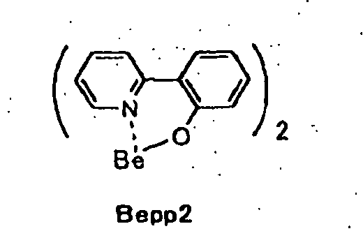
- Next, each EL device thus produced was evaluated as shown below:
The EL devices and of comparison were subjected to luminescence by applying thereto a DC constant voltage by means of a source measure unit, Model 2400 (trade name), made by Toyo Technica Co., Ltd. and the luminance that each EL device showed was measured using a luminometer BM-8 (trade name), made by Topcon Co. and emission wavelength was measured using a spectrum analyzer PMA-11 (trade name), made by Hamamatsu Photonics KK, to obtain luminous efficiency. Next, durability was evaluated as follows: First, the device was driven at the rate of 1 mA/4 mm2, and the initial luminance was measured. Then, after 200 h low-current driving of the device at the rate of 1 mA/4 mm2, luminescence was measured. The maintenance rate of luminance was obtained by comparing the 200 h luminance with the initial luminance. The results are shown in Tables 1 and 2.Table 1 Element Nos. Luminescent material (Dope concentration) Host material (Film thickness) Electron-transporting layer(Film thickness) Maintenance rate of luminance Remarks 101 Compound (65) 2% Bepp2 (40 nm) - 6% Comparative example (The element described in US 6 653 564 B1 )102 Compound (65) 5% Bepp2 (40 nm) - 11% Comparative example (The element described in US 6 653 564 B1 )103 Compound (1) 5% Bepp2 (40 nm) - 8% Comparative example (The element described in US 6 653 564 B1 )104 Compound (1) 5% Bepp2 (40 nm) Compound B (36 nm) 21% Reference example 105 Compound (1) 5% Compound A (36 nm) Compound B (36 nm) 32% Reference example Element configuration: ITO/NPD (50nm)/5wt% Luminescent material-Host material/Electron-transporting material/LiF-Al - The results demonstrate that the reference devices, containing an electron-transporting layer, exhibited an enhanced maintenance rate of luminance that led to excellent durability of the device, compared with the devices of the Comparative Examples. In addition, the durability of the device was further improved by altering the host material to a non-complex aromatic heterocyclic compound such as Compound A.
Table 2 Element Nos. Luminescent material Host material Light-emission λmax Maintenance rate of luminescence Remarks 201 Compound (1) Compound A 615 nm 81% Reference example 202 Compound (15) Compound A 586 nm 88% Reference example 204 Compound (79) Compound A 509 nm 83% This invention 205 Compound (88) Compound A 620 nm 79% Reference example 206 Compound (15) BAlq 585 nm 92% Reference example Element configuration: ITO/CuPc(10 nm)/NPD(20 nm)/5 wt% Luminescent material-Host material (30 nm)BAlq(10 nm)Alq(40 nm)/LiF-Al - Further, the results demonstrate that the use of both copper phthalocyanine (CuPc), acting as a hole-injection layer, and BAlq, acting as a hole-blocking layer, further improved on the durability of the device, and the compounds of the present invention enabled emitting red light and green light with excellent color purity. Further, the compounds of the present invention also enable emitting light of a shorter wavelength.
- The luminescent devices of the present invention are high in both external quantum efficiency and maximum luminance, and excellent in luminescent characteristics (performances). Further, the luminescent devices are excellent in durability. The luminescent device of the present invention can be preferably used in such fields as display devices, displays, backlights, electrophotography, illuminating light sources, recording light sources, exposing light sources, reading light sources, signs, signboards, interiors, and optical communications. Further, the compounds of the present invention can be utilized for the electroluminescent devices, as well as medical usage, brightening agents, photographic materials, UV absorbing materials, laser dyes, recording media materials, inkjet pigments, color filter dyes, color conversion filters, and the like. The novel complexes of the present invention are suitable for producing such excellent luminescent devices as described above.
Claims (4)
- A compound represented by formula (11):


- The compound of claim 1, wherein Rc3, Rc4, Rc5 and Rc6 are selected from the group consisting of an alkyl group, an aryl group, a hetero aryl group and a halogen atom.
- The compound of claim 1, selected from the following compounds:
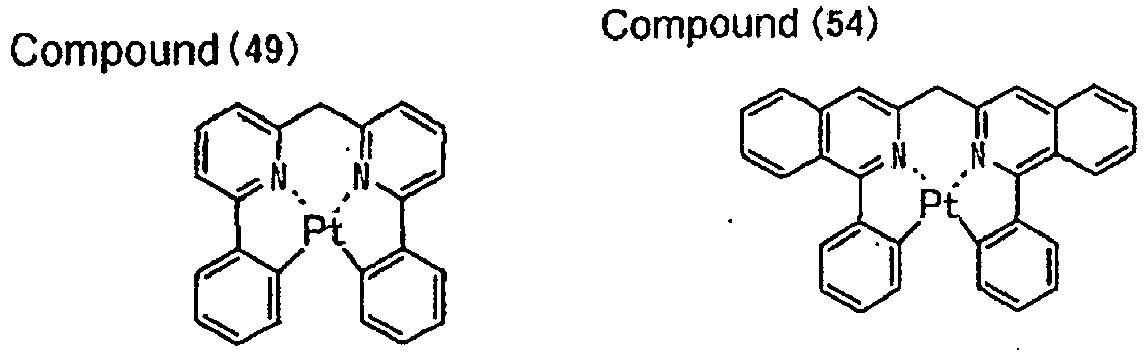


- An organic electroluminescent device, comprising a pair of electrodes and at least one organic layer including a luminescent layer between the pair of electrodes, wherein at least layer between the pair of electrodes comprises at least one metal complex as defined in any one of claims 1 to 3.
Priority Applications (4)
| Application Number | Priority Date | Filing Date | Title |
|---|---|---|---|
| EP15001367.0A EP2924094B1 (en) | 2003-06-02 | 2004-06-01 | Organic electroluminescent devices and metal complex compounds |
| EP21172459.6A EP3901235B1 (en) | 2003-06-02 | 2004-06-01 | Organic electroluminescent devices and metal complex compounds |
| EP19206006.9A EP3623444B1 (en) | 2003-06-02 | 2004-06-01 | Organic electroluminescent devices and metal complex compounds |
| EP17163955.2A EP3211057B2 (en) | 2003-06-02 | 2004-06-01 | Organic electroluminescent devices and metal complex compounds |
Applications Claiming Priority (3)
| Application Number | Priority Date | Filing Date | Title |
|---|---|---|---|
| JP2003157006 | 2003-06-02 | ||
| JP2004092274 | 2004-03-26 | ||
| PCT/JP2004/007882 WO2004108857A1 (en) | 2003-06-02 | 2004-06-01 | Organic electroluminescent devices and metal complex compounds |
Related Child Applications (6)
| Application Number | Title | Priority Date | Filing Date |
|---|---|---|---|
| EP15001367.0A Division EP2924094B1 (en) | 2003-06-02 | 2004-06-01 | Organic electroluminescent devices and metal complex compounds |
| EP15001367.0A Division-Into EP2924094B1 (en) | 2003-06-02 | 2004-06-01 | Organic electroluminescent devices and metal complex compounds |
| EP17163955.2A Division EP3211057B2 (en) | 2003-06-02 | 2004-06-01 | Organic electroluminescent devices and metal complex compounds |
| EP17163955.2A Division-Into EP3211057B2 (en) | 2003-06-02 | 2004-06-01 | Organic electroluminescent devices and metal complex compounds |
| EP21172459.6A Division EP3901235B1 (en) | 2003-06-02 | 2004-06-01 | Organic electroluminescent devices and metal complex compounds |
| EP19206006.9A Division EP3623444B1 (en) | 2003-06-02 | 2004-06-01 | Organic electroluminescent devices and metal complex compounds |
Publications (4)
| Publication Number | Publication Date |
|---|---|
| EP1629063A1 EP1629063A1 (en) | 2006-03-01 |
| EP1629063A4 EP1629063A4 (en) | 2012-03-07 |
| EP1629063B1 EP1629063B1 (en) | 2015-05-13 |
| EP1629063B2 true EP1629063B2 (en) | 2019-07-17 |
Family
ID=33513361
Family Applications (5)
| Application Number | Title | Priority Date | Filing Date |
|---|---|---|---|
| EP04735658.9A Expired - Lifetime EP1629063B2 (en) | 2003-06-02 | 2004-06-01 | Organic electroluminescent devices and metal complex compounds |
| EP19206006.9A Expired - Lifetime EP3623444B1 (en) | 2003-06-02 | 2004-06-01 | Organic electroluminescent devices and metal complex compounds |
| EP21172459.6A Expired - Lifetime EP3901235B1 (en) | 2003-06-02 | 2004-06-01 | Organic electroluminescent devices and metal complex compounds |
| EP17163955.2A Expired - Lifetime EP3211057B2 (en) | 2003-06-02 | 2004-06-01 | Organic electroluminescent devices and metal complex compounds |
| EP15001367.0A Expired - Lifetime EP2924094B1 (en) | 2003-06-02 | 2004-06-01 | Organic electroluminescent devices and metal complex compounds |
Family Applications After (4)
| Application Number | Title | Priority Date | Filing Date |
|---|---|---|---|
| EP19206006.9A Expired - Lifetime EP3623444B1 (en) | 2003-06-02 | 2004-06-01 | Organic electroluminescent devices and metal complex compounds |
| EP21172459.6A Expired - Lifetime EP3901235B1 (en) | 2003-06-02 | 2004-06-01 | Organic electroluminescent devices and metal complex compounds |
| EP17163955.2A Expired - Lifetime EP3211057B2 (en) | 2003-06-02 | 2004-06-01 | Organic electroluminescent devices and metal complex compounds |
| EP15001367.0A Expired - Lifetime EP2924094B1 (en) | 2003-06-02 | 2004-06-01 | Organic electroluminescent devices and metal complex compounds |
Country Status (5)
| Country | Link |
|---|---|
| US (7) | US7569692B2 (en) |
| EP (5) | EP1629063B2 (en) |
| JP (5) | JP5278911B2 (en) |
| KR (1) | KR101098807B1 (en) |
| WO (1) | WO2004108857A1 (en) |
Families Citing this family (146)
| Publication number | Priority date | Publication date | Assignee | Title |
|---|---|---|---|---|
| EP1620525B1 (en) | 2003-05-09 | 2011-09-28 | FUJIFILM Corporation | Organic electroluminescent device and platinum compound |
| WO2004108857A1 (en) * | 2003-06-02 | 2004-12-16 | Fuji Photo Film Co., Ltd. | Organic electroluminescent devices and metal complex compounds |
| DE10350722A1 (en) * | 2003-10-30 | 2005-05-25 | Covion Organic Semiconductors Gmbh | metal complexes |
| EP1683804B1 (en) | 2003-11-04 | 2013-07-31 | Takasago International Corporation | Platinum complex and luminescent element |
| US7332232B2 (en) * | 2004-02-03 | 2008-02-19 | Universal Display Corporation | OLEDs utilizing multidentate ligand systems |
| US8084145B2 (en) | 2004-04-02 | 2011-12-27 | Semiconductor Energy Laboratory Co., Ltd. | Organometallic complex, light emitting element using the complex, light emitting device using the element, and electric apparatus using the device |
| US7393599B2 (en) | 2004-05-18 | 2008-07-01 | The University Of Southern California | Luminescent compounds with carbene ligands |
| US7655323B2 (en) | 2004-05-18 | 2010-02-02 | The University Of Southern California | OLEDs utilizing macrocyclic ligand systems |
| GB0411580D0 (en) * | 2004-05-24 | 2004-06-23 | Cambridge Display Tech Ltd | Light-emitting device |
| JP2006093665A (en) * | 2004-08-26 | 2006-04-06 | Fuji Photo Film Co Ltd | Organic electroluminescence device |
| JP4500735B2 (en) | 2004-09-22 | 2010-07-14 | 富士フイルム株式会社 | Organic electroluminescence device |
| JP4531509B2 (en) * | 2004-09-27 | 2010-08-25 | 富士フイルム株式会社 | Light emitting element |
| US7754346B2 (en) * | 2004-11-10 | 2010-07-13 | Fujifilm Corporation | Organic electroluminescent device |
| JP4762527B2 (en) | 2004-11-10 | 2011-08-31 | 富士フイルム株式会社 | Organic electroluminescence device |
| US20060134461A1 (en) * | 2004-12-17 | 2006-06-22 | Shouquan Huo | Organometallic materials and electroluminescent devices |
| TWI258881B (en) * | 2005-01-06 | 2006-07-21 | Au Optronics Corp | Photoelectric device |
| JPWO2006082742A1 (en) * | 2005-02-04 | 2008-06-26 | コニカミノルタホールディングス株式会社 | ORGANIC ELECTROLUMINESCENT ELEMENT MATERIAL, ORGANIC ELECTROLUMINESCENT ELEMENT, DISPLAY DEVICE AND LIGHTING DEVICE |
| JP4773109B2 (en) * | 2005-02-28 | 2011-09-14 | 高砂香料工業株式会社 | Platinum complex and light emitting device |
| US7771845B2 (en) * | 2005-03-14 | 2010-08-10 | Fujifilm Corporation | Organic electroluminescent device |
| EP2562840A1 (en) | 2005-03-16 | 2013-02-27 | UDC Ireland Limited | Platinum complex compound and organic electroluminescent device |
| EP1869059B1 (en) * | 2005-03-17 | 2014-04-23 | Semiconductor Energy Laboratory Co., Ltd. | Organometallic complex, and light-emitting element, light-emitting device and electronic device using the organometallic complex |
| TWI391027B (en) | 2005-04-25 | 2013-03-21 | Fujifilm Corp | Organic electroluminescent device |
| JP4801928B2 (en) | 2005-04-25 | 2011-10-26 | 富士フイルム株式会社 | Organic electroluminescence device |
| TWI418606B (en) * | 2005-04-25 | 2013-12-11 | Udc Ireland Ltd | Organic electroluminescent device |
| US7498437B2 (en) * | 2005-04-27 | 2009-03-03 | Au Optronics Corporation | Phosphorescent light-emitting device with doped iridium-complex |
| JP4533796B2 (en) * | 2005-05-06 | 2010-09-01 | 富士フイルム株式会社 | Organic electroluminescence device |
| US20100264812A1 (en) * | 2005-09-09 | 2010-10-21 | Sumitomo Chemical Company, Limited | Metal complex, light-emitting material, and light-emitting device |
| JP2007110067A (en) * | 2005-09-14 | 2007-04-26 | Fujifilm Corp | Composition for organic electroluminescent device, method for producing organic electroluminescent device, and organic electroluminescent device |
| JP4789556B2 (en) * | 2005-09-21 | 2011-10-12 | 富士フイルム株式会社 | Organic electroluminescence device |
| US8206839B2 (en) | 2005-10-04 | 2012-06-26 | Fujifilm Corporation | Organic electroluminescent element |
| CN104497054B (en) | 2005-12-05 | 2017-09-22 | 株式会社半导体能源研究所 | Organometallic complex and use its light-emitting component, luminaire and electronic equipment |
| JP4770699B2 (en) * | 2005-12-16 | 2011-09-14 | ソニー株式会社 | Display element |
| CN101415718B (en) | 2006-02-10 | 2013-05-29 | 通用显示公司 | Cyclometallated imidazo[1,2-f]phenanthridine and diimidazo[1,2-a:1',2'-c]quinazoline ligands and their isoelectronic and benzocyclization analogs metal complexes |
| JP4871607B2 (en) | 2006-02-23 | 2012-02-08 | 富士フイルム株式会社 | Organic electroluminescence device |
| US8273467B2 (en) | 2006-02-28 | 2012-09-25 | Fujifilm Corporation | Organic electroluminescent device |
| TWI481616B (en) * | 2006-03-21 | 2015-04-21 | Semiconductor Energy Lab | Organometallic complex and light-emitting element using the same, light-emitting device and electronic device |
| JP2008037848A (en) * | 2006-08-10 | 2008-02-21 | Takasago Internatl Corp | Platinum complex and light emitting device |
| WO2008030624A2 (en) * | 2006-09-08 | 2008-03-13 | The Research Foundation Of State University Of New York | Nanoparticles for two-photon activated photodynamic therapy and imaging |
| US20080233051A1 (en) * | 2006-09-08 | 2008-09-25 | Prasad Paras N | Nanoparticles for two-photon activated photodynamic therapy and imaging |
| JP5282260B2 (en) | 2006-11-27 | 2013-09-04 | ユー・ディー・シー アイルランド リミテッド | Organic electroluminescence device |
| EP2087063B1 (en) * | 2006-11-30 | 2016-10-19 | Semiconductor Energy Laboratory Co, Ltd. | Light-emitting device |
| ATE512206T1 (en) * | 2007-03-28 | 2011-06-15 | Fujifilm Corp | ORGANIC ELECTROLUMINESCENCE DEVICE |
| JP5430073B2 (en) | 2007-03-30 | 2014-02-26 | ユー・ディー・シー アイルランド リミテッド | Organic electroluminescence device |
| DE102007017656A1 (en) * | 2007-04-12 | 2008-10-16 | Henkel Ag & Co. Kgaa | Biheteroaryl metal complexes as bleaching catalysts |
| KR20100018036A (en) * | 2007-06-05 | 2010-02-16 | 가부시키가이샤 한도오따이 에네루기 켄큐쇼 | Organometallic complex, and light-emitting material, light-emitting element, light-emitting device and electronic device |
| KR101548382B1 (en) * | 2007-09-14 | 2015-08-28 | 유디씨 아일랜드 리미티드 | Organic electroluminescence device |
| JP4579320B2 (en) * | 2007-09-14 | 2010-11-10 | 富士フイルム株式会社 | Organic electroluminescence device |
| JP5243972B2 (en) | 2008-02-28 | 2013-07-24 | ユー・ディー・シー アイルランド リミテッド | Organic electroluminescence device |
| JP4531836B2 (en) | 2008-04-22 | 2010-08-25 | 富士フイルム株式会社 | Organic electroluminescent device, novel platinum complex compound and novel compound that can be a ligand |
| JP4531842B2 (en) * | 2008-04-24 | 2010-08-25 | 富士フイルム株式会社 | Organic electroluminescence device |
| DE102008027005A1 (en) | 2008-06-05 | 2009-12-10 | Merck Patent Gmbh | Organic electronic device containing metal complexes |
| DE102008057050B4 (en) | 2008-11-13 | 2021-06-02 | Merck Patent Gmbh | Materials for organic electroluminescent devices |
| DE102008057051B4 (en) | 2008-11-13 | 2021-06-17 | Merck Patent Gmbh | Materials for organic electroluminescent devices |
| WO2010075101A2 (en) * | 2008-12-15 | 2010-07-01 | Dcb-Usa, Llc | Treating picornavirus infection by targeting microrna mir-141 |
| JP2010232163A (en) | 2009-03-03 | 2010-10-14 | Fujifilm Corp | Method of manufacturing light-emitting display device, light-emitting display device, and light-emitting display |
| DE102009013041A1 (en) | 2009-03-13 | 2010-09-16 | Merck Patent Gmbh | Materials for organic electroluminescent devices |
| JP5604505B2 (en) | 2009-04-06 | 2014-10-08 | アリゾナ ボード オブ リージェンツ アクティング フォー アンド オン ビハーフ オブ アリゾナ ステイト ユニバーシティ | Synthesis of four-coordinate platinum complexes and their application to light-emitting devices |
| JP2011046699A (en) * | 2009-07-31 | 2011-03-10 | Sumitomo Chemical Co Ltd | Metal complex, composition including the same, and light-emitting element using the same |
| EP2461387A4 (en) | 2009-07-31 | 2013-01-23 | Udc Ireland Ltd | Vapor deposition material for organic device and method for manufacturing organic device |
| DE102009042693A1 (en) | 2009-09-23 | 2011-03-24 | Merck Patent Gmbh | Materials for electronic devices |
| JP2010093294A (en) * | 2010-01-15 | 2010-04-22 | Fujifilm Corp | Organic electroluminescent light emitting element |
| US8288187B2 (en) | 2010-01-20 | 2012-10-16 | Universal Display Corporation | Electroluminescent devices for lighting applications |
| EP2550691A1 (en) * | 2010-03-23 | 2013-01-30 | Merck Patent GmbH | Materials for organic electroluminescent devices |
| KR101832003B1 (en) | 2010-03-31 | 2018-02-26 | 유디씨 아일랜드 리미티드 | Organic electric-field light-emitting device material, organic electric-field light-emitting device formed of same, and method for manufacturing organic electric-field light-emitting device |
| DE112011101526T5 (en) | 2010-04-30 | 2013-05-16 | Arizona Board Of Regents Acting For And On Behalf Of Arizona State University | Synthesis of four-coordinate palladium complexes and their applications in light-emitting devices |
| US9324957B2 (en) | 2010-04-30 | 2016-04-26 | Arizona Board Of Regents On Behalf Of Arizona State University | Synthesis of four coordinated gold complexes and their applications in light emitting devices thereof |
| TWI541247B (en) | 2011-02-18 | 2016-07-11 | 美國亞利桑那州立大學董事會 | Four-coordinate platinum and palladium complex with geometrically distortion charge transfer state and its application in illuminating devices |
| WO2012142387A1 (en) | 2011-04-14 | 2012-10-18 | Arizona Board Of Regents Acting For And On Behalf Of Arizona State University | Pyridine-oxyphenyl coordinated iridium (iii) complexes and methods of making and using |
| WO2012162488A1 (en) | 2011-05-26 | 2012-11-29 | Arizona Board Of Regents Acting For And On Behalf Of Arizona State University | Synthesis of platinum and palladium complexes as narrow-band phosphorescent emitters for full color displays |
| WO2012163471A1 (en) | 2011-06-03 | 2012-12-06 | Merck Patent Gmbh | Metal complexes |
| US9783564B2 (en) | 2011-07-25 | 2017-10-10 | Universal Display Corporation | Organic electroluminescent materials and devices |
| KR101967014B1 (en) | 2011-08-10 | 2019-04-08 | 메르크 파텐트 게엠베하 | Metal complexes |
| JP2014225484A (en) * | 2011-11-24 | 2014-12-04 | ユー・ディー・シー アイルランド リミテッド | Organic electroluminescent element, and light emitting device, display device and lighting system using the organic electroluminescent element |
| JP5913938B2 (en) | 2011-11-30 | 2016-05-11 | 富士フイルム株式会社 | Light diffusing transfer material, method of forming light diffusing layer, and method of manufacturing organic electroluminescent device |
| KR102012047B1 (en) | 2012-01-06 | 2019-08-19 | 유니버셜 디스플레이 코포레이션 | Highly efficient phosphorescent materials |
| US9386657B2 (en) | 2012-03-15 | 2016-07-05 | Universal Display Corporation | Organic Electroluminescent materials and devices |
| WO2014009715A1 (en) * | 2012-07-10 | 2014-01-16 | Cambridge Display Technology Limited | Light-emitting compound |
| US9540329B2 (en) | 2012-07-19 | 2017-01-10 | Universal Display Corporation | Organic electroluminescent materials and devices |
| US9312502B2 (en) | 2012-08-10 | 2016-04-12 | Arizona Board Of Regents Acting For And On Behalf Of Arizona State University | Iridium complexes demonstrating broadband emission through controlled geometric distortion and applications thereof |
| WO2014031977A1 (en) | 2012-08-24 | 2014-02-27 | Arizona Board Of Regents For And On Behalf Of Arizona State University | Metal compounds and methods and uses thereof |
| WO2014047616A1 (en) | 2012-09-24 | 2014-03-27 | Arizona Board Of Regents For And On Behalf Of Arizona State University | Metal compounds, methods, and uses thereof |
| US9252363B2 (en) | 2012-10-04 | 2016-02-02 | Universal Display Corporation | Aryloxyalkylcarboxylate solvent compositions for inkjet printing of organic layers |
| WO2014109814A2 (en) | 2012-10-26 | 2014-07-17 | Arizona Board Of Regents Acting For And On Behalf Of Arizona State University | Metal complexes, methods, and uses thereof |
| KR102000211B1 (en) | 2012-10-29 | 2019-09-30 | 삼성디스플레이 주식회사 | Organometallic compound and organic light emitting diode comprising the same |
| US9196860B2 (en) | 2012-12-04 | 2015-11-24 | Universal Display Corporation | Compounds for triplet-triplet annihilation upconversion |
| US8716484B1 (en) | 2012-12-05 | 2014-05-06 | Universal Display Corporation | Hole transporting materials with twisted aryl groups |
| US9653691B2 (en) | 2012-12-12 | 2017-05-16 | Universal Display Corporation | Phosphorescence-sensitizing fluorescence material system |
| KR102081280B1 (en) | 2013-01-30 | 2020-05-28 | 삼성디스플레이 주식회사 | Organic light emitting diode comprising the same |
| US10400163B2 (en) | 2013-02-08 | 2019-09-03 | Universal Display Corporation | Organic electroluminescent materials and devices |
| KR102349659B1 (en) | 2013-06-10 | 2022-01-11 | 아리조나 보드 오브 리젠츠 온 비하프 오브 아리조나 스테이트 유니버시티 | Phosphorescent tetradentate metal complexes having modified emission spectra |
| JP6804823B2 (en) * | 2013-10-14 | 2020-12-23 | アリゾナ・ボード・オブ・リージェンツ・オン・ビハーフ・オブ・アリゾナ・ステイト・ユニバーシティーArizona Board of Regents on behalf of Arizona State University | Platinum complex and device |
| US10644251B2 (en) * | 2013-12-04 | 2020-05-05 | Universal Display Corporation | Organic electroluminescent materials and devices |
| US9224963B2 (en) | 2013-12-09 | 2015-12-29 | Arizona Board Of Regents On Behalf Of Arizona State University | Stable emitters |
| US9876173B2 (en) | 2013-12-09 | 2018-01-23 | Universal Display Corporation | Organic electroluminescent materials and devices |
| US10135008B2 (en) | 2014-01-07 | 2018-11-20 | Universal Display Corporation | Organic electroluminescent materials and devices |
| US10020455B2 (en) | 2014-01-07 | 2018-07-10 | Arizona Board Of Regents On Behalf Of Arizona State University | Tetradentate platinum and palladium complex emitters containing phenyl-pyrazole and its analogues |
| US10056567B2 (en) | 2014-02-28 | 2018-08-21 | Arizona Board Of Regents On Behalf Of Arizona State University | Chiral metal complexes as emitters for organic polarized electroluminescent devices |
| US9450198B2 (en) | 2014-04-15 | 2016-09-20 | Universal Display Corporation | Organic electroluminescent materials and devices |
| US9941479B2 (en) | 2014-06-02 | 2018-04-10 | Arizona Board Of Regents On Behalf Of Arizona State University | Tetradentate cyclometalated platinum complexes containing 9,10-dihydroacridine and its analogues |
| KR102237823B1 (en) | 2014-07-09 | 2021-04-08 | 삼성전자주식회사 | Organometallic compound and organic light-emitting device including the same |
| CN105273712B (en) | 2014-07-11 | 2017-07-25 | 广东阿格蕾雅光电材料有限公司 | Luminescent materials for light-emitting diodes |
| US9923155B2 (en) | 2014-07-24 | 2018-03-20 | Arizona Board Of Regents On Behalf Of Arizona State University | Tetradentate platinum (II) complexes cyclometalated with functionalized phenyl carbene ligands and their analogues |
| US9502671B2 (en) | 2014-07-28 | 2016-11-22 | Arizona Board Of Regents On Behalf Of Arizona State University | Tridentate cyclometalated metal complexes with six-membered coordination rings |
| US9818959B2 (en) | 2014-07-29 | 2017-11-14 | Arizona Board of Regents on behlaf of Arizona State University | Metal-assisted delayed fluorescent emitters containing tridentate ligands |
| US10793546B2 (en) | 2014-08-15 | 2020-10-06 | Arizona Board Of Regents On Behalf Of Arizona State University | Non-platinum metal complexes for excimer based single dopant white organic light emitting diodes |
| US11329244B2 (en) | 2014-08-22 | 2022-05-10 | Arizona Board Of Regents On Behalf Of Arizona State University | Organic light-emitting diodes with fluorescent and phosphorescent emitters |
| US9920242B2 (en) | 2014-08-22 | 2018-03-20 | Arizona Board Of Regents On Behalf Of Arizona State University | Metal-assisted delayed fluorescent materials as co-host materials for fluorescent OLEDs |
| US10033003B2 (en) | 2014-11-10 | 2018-07-24 | Arizona Board Of Regents On Behalf Of Arizona State University | Tetradentate metal complexes with carbon group bridging ligands |
| US9865825B2 (en) | 2014-11-10 | 2018-01-09 | Arizona Board Of Regents On Behalf Of Arizona State University | Emitters based on octahedral metal complexes |
| KR101814673B1 (en) * | 2014-11-28 | 2018-01-04 | 삼성에스디아이 주식회사 | Novel compound,photosensitive resin composition comprising the same and color filter |
| KR102344885B1 (en) | 2015-01-09 | 2021-12-29 | 삼성전자주식회사 | Organometallic compound and organic light-emitting device including the same |
| US9871214B2 (en) | 2015-03-23 | 2018-01-16 | Universal Display Corporation | Organic electroluminescent materials and devices |
| US9711739B2 (en) | 2015-06-02 | 2017-07-18 | Arizona Board Of Regents On Behalf Of Arizona State University | Tetradentate metal complexes containing indoloacridine and its analogues |
| US9879039B2 (en) | 2015-06-03 | 2018-01-30 | Arizona Board Of Regents On Behalf Of Arizona State University | Tetradentate and octahedral metal complexes containing naphthyridinocarbazole and its analogues |
| US11930662B2 (en) | 2015-06-04 | 2024-03-12 | Arizona Board Of Regents On Behalf Of Arizona State University | Transparent electroluminescent devices with controlled one-side emissive displays |
| US10158091B2 (en) | 2015-08-04 | 2018-12-18 | Arizona Board Of Regents On Behalf Of Arizona State University | Tetradentate platinum (II) and palladium (II) complexes, devices, and uses thereof |
| EP3133078B1 (en) | 2015-08-18 | 2019-01-30 | Samsung Electronics Co., Ltd. | Organometallic compound and organic light-emitting device including the same |
| KR102684614B1 (en) * | 2015-12-21 | 2024-07-15 | 유디씨 아일랜드 리미티드 | Transition metal complexes with tripodal ligands and the use thereof in oleds |
| US10153442B2 (en) | 2015-12-31 | 2018-12-11 | National Tsing Hua University | Iridium complex, OLED using the same, and nitrogen-containing tridentate ligand having carbene unit |
| US11335865B2 (en) | 2016-04-15 | 2022-05-17 | Arizona Board Of Regents On Behalf Of Arizona State University | OLED with multi-emissive material layer |
| US11228003B2 (en) * | 2016-04-22 | 2022-01-18 | Universal Display Corporation | Organic electroluminescent materials and devices |
| US11228002B2 (en) * | 2016-04-22 | 2022-01-18 | Universal Display Corporation | Organic electroluminescent materials and devices |
| US10672997B2 (en) | 2016-06-20 | 2020-06-02 | Universal Display Corporation | Organic electroluminescent materials and devices |
| US10177323B2 (en) | 2016-08-22 | 2019-01-08 | Arizona Board Of Regents On Behalf Of Arizona State University | Tetradentate platinum (II) and palladium (II) complexes and octahedral iridium complexes employing azepine functional groups and their analogues |
| KR102888327B1 (en) | 2016-10-12 | 2025-11-18 | 아리조나 보드 오브 리젠츠 온 비하프 오브 아리조나 스테이트 유니버시티 | Narrow band red phosphorescent tetradentate platinum (ii) complexes |
| US11183670B2 (en) | 2016-12-16 | 2021-11-23 | Arizona Board Of Regents On Behalf Of Arizona State University | Organic light emitting diode with split emissive layer |
| US20180190915A1 (en) * | 2017-01-03 | 2018-07-05 | Universal Display Corporation | Organic electroluminescent materials and devices |
| US11765968B2 (en) * | 2017-01-23 | 2023-09-19 | Universal Display Corporation | Organic electroluminescent materials and devices |
| US11708385B2 (en) | 2017-01-27 | 2023-07-25 | Arizona Board Of Regents On Behalf Of Arizona State University | Metal-assisted delayed fluorescent emitters employing pyrido-pyrrolo-acridine and analogues |
| US10516117B2 (en) | 2017-05-19 | 2019-12-24 | Arizona Board Of Regents On Behalf Of Arizona State University | Metal-assisted delayed fluorescent emttters employing benzo-imidazo-phenanthridine and analogues |
| US11101435B2 (en) | 2017-05-19 | 2021-08-24 | Arizona Board Of Regents On Behalf Of Arizona State University | Tetradentate platinum and palladium complexes based on biscarbazole and analogues |
| US11594688B2 (en) | 2017-10-17 | 2023-02-28 | Arizona Board Of Regents On Behalf Of Arizona State University | Display and lighting devices comprising phosphorescent excimers with preferred molecular orientation as monochromatic emitters |
| US11647643B2 (en) | 2017-10-17 | 2023-05-09 | Arizona Board Of Regents On Behalf Of Arizona State University | Hole-blocking materials for organic light emitting diodes |
| KR102486392B1 (en) * | 2017-11-24 | 2023-01-09 | 삼성전자주식회사 | Organic light emitting device and method for preparing the same |
| KR102474831B1 (en) | 2017-12-08 | 2022-12-08 | 삼성디스플레이 주식회사 | Organic electroluminescence device and organometallic compound for organic electroluminescence device |
| US12037348B2 (en) | 2018-03-09 | 2024-07-16 | Arizona Board Of Regents On Behalf Of Arizona State University | Blue and narrow band green and red emitting metal complexes |
| WO2020018476A1 (en) | 2018-07-16 | 2020-01-23 | Jian Li | Fluorinated porphyrin derivatives for optoelectronic applications |
| CN110586188B (en) * | 2018-09-30 | 2022-07-01 | 邯郸学院 | Catalyst system for ethylene selective oligomerization, preparation method and ethylene oligomerization reaction method |
| US11878988B2 (en) | 2019-01-24 | 2024-01-23 | Arizona Board Of Regents On Behalf Of Arizona State University | Blue phosphorescent emitters employing functionalized imidazophenthridine and analogues |
| US11594691B2 (en) | 2019-01-25 | 2023-02-28 | Arizona Board Of Regents On Behalf Of Arizona State University | Light outcoupling efficiency of phosphorescent OLEDs by mixing horizontally aligned fluorescent emitters |
| KR102820738B1 (en) * | 2019-05-30 | 2025-06-16 | 삼성디스플레이 주식회사 | Organometallic compound and organic light emitting device including the same |
| US11785838B2 (en) | 2019-10-02 | 2023-10-10 | Arizona Board Of Regents On Behalf Of Arizona State University | Green and red organic light-emitting diodes employing excimer emitters |
| US11945985B2 (en) | 2020-05-19 | 2024-04-02 | Arizona Board Of Regents On Behalf Of Arizona State University | Metal assisted delayed fluorescent emitters for organic light-emitting diodes |
| CN113683625B (en) | 2020-05-19 | 2025-06-10 | 亚利桑那州立大学董事会 | Metal-assisted delayed fluorescence emitters for organic light emitting diodes |
| US20220013733A1 (en) * | 2020-06-16 | 2022-01-13 | Arizona Board Of Regents On Behalf Of Arizona State University | White oleds employing blue fluorescent emitters and orange phosphorescent excimers |
| KR102284600B1 (en) * | 2021-01-28 | 2021-08-02 | (주)랩토 | Organometallic complex and organic elcetroluminescent device including the same |
Family Cites Families (78)
| Publication number | Priority date | Publication date | Assignee | Title |
|---|---|---|---|---|
| US4392858A (en) | 1981-07-16 | 1983-07-12 | Sherwood Medical Company | Wound drainage device |
| HU199443B (en) | 1984-06-25 | 1990-02-28 | Chinoin Gyogyszer Es Vegyeszet | Bactericidal and/or fungicidal synergic plant protective comprising nitrofuran derivatives |
| JP2891783B2 (en) | 1991-02-06 | 1999-05-17 | パイオニア株式会社 | Organic electroluminescence device |
| EP0723701B1 (en) * | 1994-08-11 | 2000-01-12 | Koninklijke Philips Electronics N.V. | Solid-state image intensifier and x-ray examination apparatus comprising a solid-state image intensifier |
| GB9601603D0 (en) | 1996-01-26 | 1996-03-27 | Isis Innovations Ltd | Terpyridine-platinum (II) complexes |
| JP3195265B2 (en) | 1997-01-18 | 2001-08-06 | 東京応化工業株式会社 | Coating solution for forming Bi-based ferroelectric thin film, ferroelectric thin film formed using the same, and ferroelectric memory |
| US6303238B1 (en) | 1997-12-01 | 2001-10-16 | The Trustees Of Princeton University | OLEDs doped with phosphorescent compounds |
| DE19829948A1 (en) | 1998-07-04 | 2000-01-05 | Bayer Ag | Electroluminescent device using azomethine metal complexes |
| US6316130B1 (en) * | 1998-07-04 | 2001-11-13 | Bayer Aktiengesellschaft | Electroluminescent assemblies using azomethine-metal complexes |
| US6159888A (en) * | 1998-09-09 | 2000-12-12 | Phillips Petroleum Company | Polymerization catalyst systems, their preparation, and use |
| JP2000091084A (en) * | 1998-09-16 | 2000-03-31 | Trustees Of Princeton Univ | Ball injection improved electrode |
| KR101166264B1 (en) | 1999-03-23 | 2012-07-17 | 유니버시티 오브 서던 캘리포니아 | Cyclometallated metal complexes as phosphorescent dopants in organic leds |
| KR100913568B1 (en) | 1999-05-13 | 2009-08-26 | 더 트러스티즈 오브 프린스턴 유니버시티 | Very high efficiency organic light emitting devices based on electrophosphorescence |
| US6310360B1 (en) | 1999-07-21 | 2001-10-30 | The Trustees Of Princeton University | Intersystem crossing agents for efficient utilization of excitons in organic light emitting devices |
| GB0007002D0 (en) * | 2000-03-22 | 2000-05-10 | Borealis Polymers Oy | Catalysts |
| JP4048521B2 (en) * | 2000-05-02 | 2008-02-20 | 富士フイルム株式会社 | Light emitting element |
| DE10023174A1 (en) | 2000-05-11 | 2001-11-22 | Bosch Gmbh Robert | Electric hand tool, e.g. drill with speed control has automatic reset for adjuster, returning it to initial setting in accordance with an operational parameter |
| JP4504512B2 (en) | 2000-05-30 | 2010-07-14 | 三井化学株式会社 | Organic electroluminescence device |
| JP4344494B2 (en) * | 2000-08-24 | 2009-10-14 | 富士フイルム株式会社 | Light emitting device and novel polymer element |
| JP4154140B2 (en) | 2000-09-26 | 2008-09-24 | キヤノン株式会社 | Metal coordination compounds |
| JP4086499B2 (en) * | 2000-11-29 | 2008-05-14 | キヤノン株式会社 | Metal coordination compound, light emitting device and display device |
| DE10104426A1 (en) | 2001-02-01 | 2002-08-08 | Covion Organic Semiconductors | Process for the production of high-purity, tris-ortho-metallated organo-iridium compounds |
| JP3965319B2 (en) | 2001-03-08 | 2007-08-29 | ザ ユニヴァーシティ オブ ホンコン | Organometallic light emitting material |
| JP2002305083A (en) | 2001-04-04 | 2002-10-18 | Mitsubishi Chemicals Corp | Organic electroluminescent device |
| JP4006266B2 (en) | 2001-06-15 | 2007-11-14 | キヤノン株式会社 | Light emitting device and method for manufacturing light emitting device |
| JP4310077B2 (en) * | 2001-06-19 | 2009-08-05 | キヤノン株式会社 | Metal coordination compound and organic light emitting device |
| JP2003133071A (en) * | 2001-08-13 | 2003-05-09 | Victor Co Of Japan Ltd | Organic electroluminescent element and its manufacturing method |
| JP4409942B2 (en) * | 2001-08-29 | 2010-02-03 | ザ トラスティーズ オブ プリンストン ユニバーシテイ | Organic light-emitting device having a carrier transport layer containing a metal complex |
| JP2003073355A (en) * | 2001-09-04 | 2003-03-12 | Toyota Central Res & Dev Lab Inc | Metal complex compound and organic electroluminescent device using the same |
| JP3840085B2 (en) | 2001-10-09 | 2006-11-01 | キヤノン株式会社 | Organic light emitting device |
| JP2003123981A (en) * | 2001-10-12 | 2003-04-25 | Canon Inc | Organic light emitting device |
| JP4467876B2 (en) * | 2001-10-30 | 2010-05-26 | 株式会社半導体エネルギー研究所 | Light emitting device |
| JP3863759B2 (en) * | 2001-11-09 | 2006-12-27 | 竹子 松村 | Organic electroluminescent material using high-brightness organic iridium complex and method for producing organic electroluminescent element |
| JP3952140B2 (en) | 2001-11-22 | 2007-08-01 | 三甲株式会社 | Card holder |
| JP2004006066A (en) * | 2002-04-15 | 2004-01-08 | Sony Corp | Organic electroluminescent element and light emitting device |
| US6653654B1 (en) | 2002-05-01 | 2003-11-25 | The University Of Hong Kong | Electroluminescent materials |
| JP2004047387A (en) * | 2002-07-15 | 2004-02-12 | Fuji Electric Holdings Co Ltd | Organic multicolor light emitting display device and method of manufacturing the same |
| SE523028C2 (en) * | 2002-07-18 | 2004-03-23 | Sonnie Hermansson | Device for closing a vehicle door, a vehicle with a door and method for mounting a device for opening and closing a door |
| WO2004017137A1 (en) * | 2002-07-22 | 2004-02-26 | Idemitsu Kosan Co., Ltd. | Organic electroluminescence device |
| AU2003275645A1 (en) | 2002-11-01 | 2004-05-25 | Japan Broadcasting Corporation | Luminescents |
| DE10310887A1 (en) * | 2003-03-11 | 2004-09-30 | Covion Organic Semiconductors Gmbh | Matallkomplexe |
| JP2004331506A (en) | 2003-03-11 | 2004-11-25 | Nippon Kasei Chem Co Ltd | Epoxy terminal (meth) acrylate |
| US6833202B2 (en) * | 2003-03-13 | 2004-12-21 | City University Of Hong Kong | Electroluminescent devices |
| JP2004331508A (en) * | 2003-04-30 | 2004-11-25 | Takasago Internatl Corp | Platinum complex |
| DE10320259A1 (en) * | 2003-05-07 | 2004-11-25 | Bayer Technology Services Gmbh | Novel glucose dehydrogenase and its production |
| EP1620525B1 (en) * | 2003-05-09 | 2011-09-28 | FUJIFILM Corporation | Organic electroluminescent device and platinum compound |
| JP4460952B2 (en) | 2003-06-02 | 2010-05-12 | 富士フイルム株式会社 | Organic electroluminescent device and complex compound |
| WO2004108857A1 (en) * | 2003-06-02 | 2004-12-16 | Fuji Photo Film Co., Ltd. | Organic electroluminescent devices and metal complex compounds |
| DE10350722A1 (en) * | 2003-10-30 | 2005-05-25 | Covion Organic Semiconductors Gmbh | metal complexes |
| EP1683804B1 (en) | 2003-11-04 | 2013-07-31 | Takasago International Corporation | Platinum complex and luminescent element |
| US7029766B2 (en) * | 2003-12-05 | 2006-04-18 | Eastman Kodak Company | Organic element for electroluminescent devices |
| KR100537621B1 (en) | 2004-02-02 | 2005-12-19 | 삼성에스디아이 주식회사 | Iridium compound and organic electroluminescent display device using the same |
| US7332232B2 (en) * | 2004-02-03 | 2008-02-19 | Universal Display Corporation | OLEDs utilizing multidentate ligand systems |
| US20050170206A1 (en) * | 2004-02-03 | 2005-08-04 | Bin Ma | OLEDs utilizing multidentate ligand systems |
| US7361415B2 (en) * | 2004-04-16 | 2008-04-22 | The University Of Hong Kong | System and method for producing light with organic light-emitting devices |
| US7579090B2 (en) * | 2004-09-20 | 2009-08-25 | Eastman Kodak Company | Organic element for electroluminescent devices |
| JP4500735B2 (en) | 2004-09-22 | 2010-07-14 | 富士フイルム株式会社 | Organic electroluminescence device |
| JP4531509B2 (en) | 2004-09-27 | 2010-08-25 | 富士フイルム株式会社 | Light emitting element |
| JP2006120811A (en) | 2004-10-21 | 2006-05-11 | Canon Inc | Light emitting element and display device |
| US20060134461A1 (en) * | 2004-12-17 | 2006-06-22 | Shouquan Huo | Organometallic materials and electroluminescent devices |
| US7597967B2 (en) * | 2004-12-17 | 2009-10-06 | Eastman Kodak Company | Phosphorescent OLEDs with exciton blocking layer |
| JP2006182921A (en) * | 2004-12-28 | 2006-07-13 | Konica Minolta Holdings Inc | Organic EL element material, organic EL element, display device and lighting device |
| JP4399429B2 (en) | 2005-03-16 | 2010-01-13 | 富士フイルム株式会社 | Organic electroluminescence device |
| JP4399382B2 (en) | 2005-03-16 | 2010-01-13 | 富士フイルム株式会社 | Organic electroluminescence device |
| EP2562840A1 (en) | 2005-03-16 | 2013-02-27 | UDC Ireland Limited | Platinum complex compound and organic electroluminescent device |
| JP4934345B2 (en) | 2005-04-25 | 2012-05-16 | 富士フイルム株式会社 | Organic electroluminescence device |
| US7758971B2 (en) | 2005-04-25 | 2010-07-20 | Fujifilm Corporation | Organic electroluminescent device |
| JP2007073845A (en) | 2005-09-08 | 2007-03-22 | Fujifilm Holdings Corp | Organic laser oscillator |
| JP2008037848A (en) | 2006-08-10 | 2008-02-21 | Takasago Internatl Corp | Platinum complex and light emitting device |
| JP2008103535A (en) | 2006-10-19 | 2008-05-01 | Takasago Internatl Corp | Light emitting element |
| JP5282260B2 (en) * | 2006-11-27 | 2013-09-04 | ユー・ディー・シー アイルランド リミテッド | Organic electroluminescence device |
| KR101548382B1 (en) * | 2007-09-14 | 2015-08-28 | 유디씨 아일랜드 리미티드 | Organic electroluminescence device |
| CN101873968A (en) | 2007-11-26 | 2010-10-27 | 埃克森美孚石油公司 | Labeling method and device |
| JP5610848B2 (en) * | 2009-06-11 | 2014-10-22 | ユー・ディー・シー アイルランド リミテッド | Organic electroluminescence device |
| JP5735229B2 (en) * | 2009-07-31 | 2015-06-17 | ユー・ディー・シー アイルランド リミテッド | Organic electroluminescence device |
| JP4551480B1 (en) * | 2009-08-31 | 2010-09-29 | 富士フイルム株式会社 | Organic electroluminescence device |
| JP5770441B2 (en) * | 2009-09-30 | 2015-08-26 | ユー・ディー・シー アイルランド リミテッド | Material for organic electroluminescence device and organic electroluminescence device |
| KR102673810B1 (en) * | 2016-09-27 | 2024-06-10 | 삼성전자주식회사 | Organometallic compound, organic light emitting device including the same and a composition for diagnosing including the same |
-
2004
- 2004-06-01 WO PCT/JP2004/007882 patent/WO2004108857A1/en not_active Ceased
- 2004-06-01 EP EP04735658.9A patent/EP1629063B2/en not_active Expired - Lifetime
- 2004-06-01 EP EP19206006.9A patent/EP3623444B1/en not_active Expired - Lifetime
- 2004-06-01 EP EP21172459.6A patent/EP3901235B1/en not_active Expired - Lifetime
- 2004-06-01 EP EP17163955.2A patent/EP3211057B2/en not_active Expired - Lifetime
- 2004-06-01 EP EP15001367.0A patent/EP2924094B1/en not_active Expired - Lifetime
- 2004-06-01 US US10/551,653 patent/US7569692B2/en not_active Expired - Lifetime
-
2005
- 2005-11-18 KR KR1020057022089A patent/KR101098807B1/en not_active Expired - Lifetime
-
2009
- 2009-02-27 US US12/395,358 patent/US8211553B2/en not_active Expired - Lifetime
- 2009-10-26 JP JP2009245769A patent/JP5278911B2/en not_active Expired - Lifetime
- 2009-12-24 JP JP2009293567A patent/JP2010080982A/en active Pending
- 2009-12-24 JP JP2009293566A patent/JP5081221B2/en not_active Expired - Lifetime
-
2012
- 2012-03-14 US US13/420,289 patent/US8940415B2/en not_active Expired - Lifetime
- 2012-09-28 JP JP2012216750A patent/JP2013048256A/en active Pending
- 2012-09-28 JP JP2012216751A patent/JP2013033985A/en active Pending
-
2014
- 2014-11-26 US US14/554,725 patent/US10153444B2/en not_active Expired - Lifetime
-
2017
- 2017-11-29 US US15/825,566 patent/US10396299B2/en not_active Expired - Lifetime
-
2019
- 2019-07-31 US US16/527,363 patent/US11393989B2/en not_active Expired - Lifetime
-
2022
- 2022-06-30 US US17/854,874 patent/US20220344601A1/en not_active Abandoned
Also Published As
Similar Documents
| Publication | Publication Date | Title |
|---|---|---|
| EP1629063B1 (en) | Organic electroluminescent devices and metal complex compounds | |
| JP4340401B2 (en) | Light emitting device and iridium complex | |
| EP1919928B1 (en) | Platinum complex compound and organic electroluminescent device | |
| US7306856B2 (en) | Light-emitting element and iridium complex | |
| US8609259B2 (en) | Organic electroluminescent device and platinum compound | |
| JP4048525B2 (en) | Novel indole derivative and light emitting device using the same | |
| JP2002193952A (en) | New nitrogen-containing heterocyclic compound, material for light emitting element and light emitting elements using them | |
| JP2000351966A (en) | Specific silane compound, light emission element material comprising the same and light emission element containing the same | |
| JP2001055447A (en) | Arylsilane compound, light emitting device material and light emitting device using the same | |
| EP1652241B1 (en) | Organic electroluminescent device | |
| JP2001247858A (en) | Benzimidazole derivative, luminescent element material and luminescent element | |
| US20070232800A1 (en) | Organic electroluminescent device, and azepine compound and method for producing the same | |
| JP2001031961A (en) | Novel methine compound, luminescent element material, and luminescent element prepared from the material | |
| JP4700029B2 (en) | Light emitting element | |
| JPH11185959A (en) | Styryl compound and manufacture thereof and electroluminescent element employing the same |
Legal Events
| Date | Code | Title | Description |
|---|---|---|---|
| PUAI | Public reference made under article 153(3) epc to a published international application that has entered the european phase |
Free format text: ORIGINAL CODE: 0009012 |
|
| 17P | Request for examination filed |
Effective date: 20051122 |
|
| AK | Designated contracting states |
Kind code of ref document: A1 Designated state(s): AT BE BG CH CY CZ DE DK EE ES FI FR GB GR HU IE IT LI LU MC NL PL PT RO SE SI SK TR |
|
| DAX | Request for extension of the european patent (deleted) | ||
| RAP1 | Party data changed (applicant data changed or rights of an application transferred) |
Owner name: FUJIFILM CORPORATION |
|
| A4 | Supplementary search report drawn up and despatched |
Effective date: 20120202 |
|
| RIC1 | Information provided on ipc code assigned before grant |
Ipc: C07D 213/53 20060101ALI20120127BHEP Ipc: C07D 213/74 20060101ALI20120127BHEP Ipc: C07F 15/00 20060101ALI20120127BHEP Ipc: C09K 11/06 20060101AFI20120127BHEP Ipc: H05B 33/14 20060101ALI20120127BHEP Ipc: C07D 207/20 20060101ALI20120127BHEP Ipc: C07D 471/04 20060101ALI20120127BHEP |
|
| 17Q | First examination report despatched |
Effective date: 20120716 |
|
| RAP1 | Party data changed (applicant data changed or rights of an application transferred) |
Owner name: UDC IRELAND LIMITED |
|
| GRAP | Despatch of communication of intention to grant a patent |
Free format text: ORIGINAL CODE: EPIDOSNIGR1 |
|
| RIC1 | Information provided on ipc code assigned before grant |
Ipc: C07D 213/53 20060101ALI20141114BHEP Ipc: C09K 11/06 20060101AFI20141114BHEP Ipc: C07F 15/00 20060101ALI20141114BHEP Ipc: C07D 471/04 20060101ALI20141114BHEP Ipc: C07D 207/20 20060101ALI20141114BHEP Ipc: C07C 251/24 20060101ALI20141114BHEP Ipc: C07D 213/74 20060101ALI20141114BHEP Ipc: C07D 213/22 20060101ALI20141114BHEP |
|
| INTG | Intention to grant announced |
Effective date: 20141205 |
|
| GRAS | Grant fee paid |
Free format text: ORIGINAL CODE: EPIDOSNIGR3 |
|
| GRAA | (expected) grant |
Free format text: ORIGINAL CODE: 0009210 |
|
| AK | Designated contracting states |
Kind code of ref document: B1 Designated state(s): AT BE BG CH CY CZ DE DK EE ES FI FR GB GR HU IE IT LI LU MC NL PL PT RO SE SI SK TR |
|
| REG | Reference to a national code |
Ref country code: GB Ref legal event code: FG4D |
|
| REG | Reference to a national code |
Ref country code: CH Ref legal event code: EP |
|
| REG | Reference to a national code |
Ref country code: IE Ref legal event code: FG4D |
|
| REG | Reference to a national code |
Ref country code: FR Ref legal event code: PLFP Year of fee payment: 12 |
|
| REG | Reference to a national code |
Ref country code: AT Ref legal event code: REF Ref document number: 726845 Country of ref document: AT Kind code of ref document: T Effective date: 20150615 |
|
| REG | Reference to a national code |
Ref country code: DE Ref legal event code: R096 Ref document number: 602004047175 Country of ref document: DE Effective date: 20150625 |
|
| REG | Reference to a national code |
Ref country code: AT Ref legal event code: MK05 Ref document number: 726845 Country of ref document: AT Kind code of ref document: T Effective date: 20150513 |
|
| REG | Reference to a national code |
Ref country code: NL Ref legal event code: MP Effective date: 20150513 |
|
| PG25 | Lapsed in a contracting state [announced via postgrant information from national office to epo] |
Ref country code: PT Free format text: LAPSE BECAUSE OF FAILURE TO SUBMIT A TRANSLATION OF THE DESCRIPTION OR TO PAY THE FEE WITHIN THE PRESCRIBED TIME-LIMIT Effective date: 20150914 Ref country code: FI Free format text: LAPSE BECAUSE OF FAILURE TO SUBMIT A TRANSLATION OF THE DESCRIPTION OR TO PAY THE FEE WITHIN THE PRESCRIBED TIME-LIMIT Effective date: 20150513 Ref country code: ES Free format text: LAPSE BECAUSE OF FAILURE TO SUBMIT A TRANSLATION OF THE DESCRIPTION OR TO PAY THE FEE WITHIN THE PRESCRIBED TIME-LIMIT Effective date: 20150513 |
|
| PG25 | Lapsed in a contracting state [announced via postgrant information from national office to epo] |
Ref country code: BG Free format text: LAPSE BECAUSE OF FAILURE TO SUBMIT A TRANSLATION OF THE DESCRIPTION OR TO PAY THE FEE WITHIN THE PRESCRIBED TIME-LIMIT Effective date: 20150813 Ref country code: GR Free format text: LAPSE BECAUSE OF FAILURE TO SUBMIT A TRANSLATION OF THE DESCRIPTION OR TO PAY THE FEE WITHIN THE PRESCRIBED TIME-LIMIT Effective date: 20150814 Ref country code: AT Free format text: LAPSE BECAUSE OF FAILURE TO SUBMIT A TRANSLATION OF THE DESCRIPTION OR TO PAY THE FEE WITHIN THE PRESCRIBED TIME-LIMIT Effective date: 20150513 |
|
| REG | Reference to a national code |
Ref country code: DE Ref legal event code: R026 Ref document number: 602004047175 Country of ref document: DE |
|
| PG25 | Lapsed in a contracting state [announced via postgrant information from national office to epo] |
Ref country code: EE Free format text: LAPSE BECAUSE OF FAILURE TO SUBMIT A TRANSLATION OF THE DESCRIPTION OR TO PAY THE FEE WITHIN THE PRESCRIBED TIME-LIMIT Effective date: 20150513 Ref country code: DK Free format text: LAPSE BECAUSE OF FAILURE TO SUBMIT A TRANSLATION OF THE DESCRIPTION OR TO PAY THE FEE WITHIN THE PRESCRIBED TIME-LIMIT Effective date: 20150513 Ref country code: IT Free format text: LAPSE BECAUSE OF FAILURE TO SUBMIT A TRANSLATION OF THE DESCRIPTION OR TO PAY THE FEE WITHIN THE PRESCRIBED TIME-LIMIT Effective date: 20150513 |
|
| REG | Reference to a national code |
Ref country code: CH Ref legal event code: PL |
|
| PLBI | Opposition filed |
Free format text: ORIGINAL CODE: 0009260 |
|
| PG25 | Lapsed in a contracting state [announced via postgrant information from national office to epo] |
Ref country code: SK Free format text: LAPSE BECAUSE OF FAILURE TO SUBMIT A TRANSLATION OF THE DESCRIPTION OR TO PAY THE FEE WITHIN THE PRESCRIBED TIME-LIMIT Effective date: 20150513 Ref country code: MC Free format text: LAPSE BECAUSE OF FAILURE TO SUBMIT A TRANSLATION OF THE DESCRIPTION OR TO PAY THE FEE WITHIN THE PRESCRIBED TIME-LIMIT Effective date: 20150513 Ref country code: PL Free format text: LAPSE BECAUSE OF FAILURE TO SUBMIT A TRANSLATION OF THE DESCRIPTION OR TO PAY THE FEE WITHIN THE PRESCRIBED TIME-LIMIT Effective date: 20150513 Ref country code: CZ Free format text: LAPSE BECAUSE OF FAILURE TO SUBMIT A TRANSLATION OF THE DESCRIPTION OR TO PAY THE FEE WITHIN THE PRESCRIBED TIME-LIMIT Effective date: 20150513 Ref country code: RO Free format text: LAPSE BECAUSE OF NON-PAYMENT OF DUE FEES Effective date: 20150513 |
|
| 26 | Opposition filed |
Opponent name: MERCK PATENT GMBH Effective date: 20160127 |
|
| PLAX | Notice of opposition and request to file observation + time limit sent |
Free format text: ORIGINAL CODE: EPIDOSNOBS2 |
|
| REG | Reference to a national code |
Ref country code: IE Ref legal event code: MM4A |
|
| GBPC | Gb: european patent ceased through non-payment of renewal fee |
Effective date: 20150813 |
|
| PG25 | Lapsed in a contracting state [announced via postgrant information from national office to epo] |
Ref country code: IE Free format text: LAPSE BECAUSE OF NON-PAYMENT OF DUE FEES Effective date: 20150601 Ref country code: CH Free format text: LAPSE BECAUSE OF NON-PAYMENT OF DUE FEES Effective date: 20150630 Ref country code: LI Free format text: LAPSE BECAUSE OF NON-PAYMENT OF DUE FEES Effective date: 20150630 |
|
| REG | Reference to a national code |
Ref country code: FR Ref legal event code: PLFP Year of fee payment: 13 |
|
| PG25 | Lapsed in a contracting state [announced via postgrant information from national office to epo] |
Ref country code: SI Free format text: LAPSE BECAUSE OF FAILURE TO SUBMIT A TRANSLATION OF THE DESCRIPTION OR TO PAY THE FEE WITHIN THE PRESCRIBED TIME-LIMIT Effective date: 20150513 |
|
| PLAF | Information modified related to communication of a notice of opposition and request to file observations + time limit |
Free format text: ORIGINAL CODE: EPIDOSCOBS2 |
|
| PG25 | Lapsed in a contracting state [announced via postgrant information from national office to epo] |
Ref country code: GB Free format text: LAPSE BECAUSE OF NON-PAYMENT OF DUE FEES Effective date: 20150813 |
|
| PG25 | Lapsed in a contracting state [announced via postgrant information from national office to epo] |
Ref country code: BE Free format text: LAPSE BECAUSE OF FAILURE TO SUBMIT A TRANSLATION OF THE DESCRIPTION OR TO PAY THE FEE WITHIN THE PRESCRIBED TIME-LIMIT Effective date: 20150513 |
|
| PLBB | Reply of patent proprietor to notice(s) of opposition received |
Free format text: ORIGINAL CODE: EPIDOSNOBS3 |
|
| REG | Reference to a national code |
Ref country code: FR Ref legal event code: PLFP Year of fee payment: 14 |
|
| PG25 | Lapsed in a contracting state [announced via postgrant information from national office to epo] |
Ref country code: HU Free format text: LAPSE BECAUSE OF FAILURE TO SUBMIT A TRANSLATION OF THE DESCRIPTION OR TO PAY THE FEE WITHIN THE PRESCRIBED TIME-LIMIT; INVALID AB INITIO Effective date: 20040601 |
|
| PG25 | Lapsed in a contracting state [announced via postgrant information from national office to epo] |
Ref country code: NL Free format text: LAPSE BECAUSE OF FAILURE TO SUBMIT A TRANSLATION OF THE DESCRIPTION OR TO PAY THE FEE WITHIN THE PRESCRIBED TIME-LIMIT Effective date: 20150513 Ref country code: CY Free format text: LAPSE BECAUSE OF FAILURE TO SUBMIT A TRANSLATION OF THE DESCRIPTION OR TO PAY THE FEE WITHIN THE PRESCRIBED TIME-LIMIT Effective date: 20150513 Ref country code: SE Free format text: LAPSE BECAUSE OF FAILURE TO SUBMIT A TRANSLATION OF THE DESCRIPTION OR TO PAY THE FEE WITHIN THE PRESCRIBED TIME-LIMIT Effective date: 20150513 |
|
| PG25 | Lapsed in a contracting state [announced via postgrant information from national office to epo] |
Ref country code: TR Free format text: LAPSE BECAUSE OF FAILURE TO SUBMIT A TRANSLATION OF THE DESCRIPTION OR TO PAY THE FEE WITHIN THE PRESCRIBED TIME-LIMIT Effective date: 20150513 |
|
| PG25 | Lapsed in a contracting state [announced via postgrant information from national office to epo] |
Ref country code: LU Free format text: LAPSE BECAUSE OF NON-PAYMENT OF DUE FEES Effective date: 20150601 |
|
| REG | Reference to a national code |
Ref country code: FR Ref legal event code: PLFP Year of fee payment: 15 |
|
| PLAY | Examination report in opposition despatched + time limit |
Free format text: ORIGINAL CODE: EPIDOSNORE2 |
|
| PLBC | Reply to examination report in opposition received |
Free format text: ORIGINAL CODE: EPIDOSNORE3 |
|
| APBM | Appeal reference recorded |
Free format text: ORIGINAL CODE: EPIDOSNREFNO |
|
| APBP | Date of receipt of notice of appeal recorded |
Free format text: ORIGINAL CODE: EPIDOSNNOA2O |
|
| APAH | Appeal reference modified |
Free format text: ORIGINAL CODE: EPIDOSCREFNO |
|
| APBU | Appeal procedure closed |
Free format text: ORIGINAL CODE: EPIDOSNNOA9O |
|
| PUAH | Patent maintained in amended form |
Free format text: ORIGINAL CODE: 0009272 |
|
| STAA | Information on the status of an ep patent application or granted ep patent |
Free format text: STATUS: PATENT MAINTAINED AS AMENDED |
|
| 27A | Patent maintained in amended form |
Effective date: 20190717 |
|
| AK | Designated contracting states |
Kind code of ref document: B2 Designated state(s): AT BE BG CH CY CZ DE DK EE ES FI FR GB GR HU IE IT LI LU MC NL PL PT RO SE SI SK TR |
|
| REG | Reference to a national code |
Ref country code: DE Ref legal event code: R102 Ref document number: 602004047175 Country of ref document: DE |
|
| P01 | Opt-out of the competence of the unified patent court (upc) registered |
Effective date: 20230421 |
|
| PGFP | Annual fee paid to national office [announced via postgrant information from national office to epo] |
Ref country code: FR Payment date: 20230626 Year of fee payment: 20 Ref country code: DE Payment date: 20230626 Year of fee payment: 20 |
|
| REG | Reference to a national code |
Ref country code: DE Ref legal event code: R071 Ref document number: 602004047175 Country of ref document: DE |