EP1622263A1 - Surface mounted crystal unit - Google Patents
Surface mounted crystal unit Download PDFInfo
- Publication number
- EP1622263A1 EP1622263A1 EP05254717A EP05254717A EP1622263A1 EP 1622263 A1 EP1622263 A1 EP 1622263A1 EP 05254717 A EP05254717 A EP 05254717A EP 05254717 A EP05254717 A EP 05254717A EP 1622263 A1 EP1622263 A1 EP 1622263A1
- Authority
- EP
- European Patent Office
- Prior art keywords
- lead terminal
- sealing glass
- tip end
- base
- casing wall
- Prior art date
- Legal status (The legal status is an assumption and is not a legal conclusion. Google has not performed a legal analysis and makes no representation as to the accuracy of the status listed.)
- Withdrawn
Links
Images


Classifications
-
- H—ELECTRICITY
- H03—ELECTRONIC CIRCUITRY
- H03H—IMPEDANCE NETWORKS, e.g. RESONANT CIRCUITS; RESONATORS
- H03H9/00—Networks comprising electromechanical or electro-acoustic elements; Electromechanical resonators
- H03H9/15—Constructional features of resonators consisting of piezoelectric or electrostrictive material
- H03H9/17—Constructional features of resonators consisting of piezoelectric or electrostrictive material having a single resonator
- H03H9/19—Constructional features of resonators consisting of piezoelectric or electrostrictive material having a single resonator consisting of quartz
-
- H—ELECTRICITY
- H03—ELECTRONIC CIRCUITRY
- H03H—IMPEDANCE NETWORKS, e.g. RESONANT CIRCUITS; RESONATORS
- H03H9/00—Networks comprising electromechanical or electro-acoustic elements; Electromechanical resonators
- H03H9/02—Details
- H03H9/05—Holders or supports
- H03H9/10—Mounting in enclosures
- H03H9/1007—Mounting in enclosures for bulk acoustic wave [BAW] devices
- H03H9/1014—Mounting in enclosures for bulk acoustic wave [BAW] devices the enclosure being defined by a frame built on a substrate and a cap, the frame having no mechanical contact with the BAW device
-
- H—ELECTRICITY
- H03—ELECTRONIC CIRCUITRY
- H03H—IMPEDANCE NETWORKS, e.g. RESONANT CIRCUITS; RESONATORS
- H03H9/00—Networks comprising electromechanical or electro-acoustic elements; Electromechanical resonators
- H03H9/02—Details
-
- H—ELECTRICITY
- H03—ELECTRONIC CIRCUITRY
- H03H—IMPEDANCE NETWORKS, e.g. RESONANT CIRCUITS; RESONATORS
- H03H9/00—Networks comprising electromechanical or electro-acoustic elements; Electromechanical resonators
- H03H9/02—Details
- H03H9/05—Holders or supports
- H03H9/0504—Holders or supports for bulk acoustic wave devices
- H03H9/0514—Holders or supports for bulk acoustic wave devices consisting of mounting pads or bumps
Definitions
- the present invention relates to a surface mounting base for an oscillator that uses a J lead terminal, and to a crystal oscillator that uses the surface mounting base (hereinafter, referred to as a "surface mounted crystal unit"), and in particular to a surface mounted crystal unit having excellent compatibility with a set substrate that mounts the surface mounted crystal unit.
- a surface mounted crystal unit is small in size and is light weight, it is used particularly inside portable electronic devices.
- a crystal element is mounted on a surface mounting base and is hermetically sealed.
- a surface mounting base that takes into consideration its compatibility with a set substrate on which the surface mounted crystal unit is mounted, has been proposed (see Japanese Unexamined Laid-open Patent Publication No. 2003-297453).
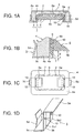
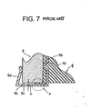
- FIG. 5 is a diagram for explaining a conventional example, wherein FIG. 5A is a vertical sectional view of a conventional surface mounted crystal unit, and FIG. 5B is a plan view of the crystal element thereof.
- the surface mounted crystal unit is constructed such that a crystal element 2 is mounted on a surface mounting base 1 and is covered and hermetically sealed with a cover 3.
- the surface mounting base 1 comprises an insulation base 4, lead terminals 5, and a sealing glass 6.
- the insulation base 4 is made from alumina ceramic for example, and has a pair of through holes 7 on its opposite end sides. In these pair of through holes 7, the sealing glass 6 with the lead terminals 5 passing therethrough, is embedded in gaps between the through holes 7 and the lead terminals 5, forming a so-called airtight terminal.
- Each lead terminal 5 is made from metal such as Cu, and has a crank shaped cross-section as shown in FIG. 5A, and comprises a holding part 5a, a through part 5b, and a mounting terminal part 5c.
- the holding part 5a and the mounting terminal part 5c are formed bent in horizontally reversed directions on the top and bottom sides of the through part 5b, as shown in the diagram.
- the sealing glass 6 is made from solid state powdered glass, and is poured into the pair of through holes 7, and is melted integrally with the insulation base 4 and the lead terminals 5.
- the crystal element 2 is, for example, an AT-cut crystal as shown in FIG. 5B. Its both principal surfaces have an excitation electrode 8, from both ends of which extension electrodes 9 extend,. In addition, both end parts of the crystal element 2 from which the extension electrodes 9 extend are fixed to the holding part 5a of the lead terminal 5 by an electrically conductive adhesive (not shown).
- the cover 3 is made from insulating material such as ceramic, and as shown in FIG. 5A, is bonded on the periphery, which is one principal surface side of the surface mounting base 1 (insulation base 4), by glass sealing for example.
- the mounting terminal part 5c of the lead terminal 5 is bonded on a circuit terminal part of a set substrate (not shown) by means of soldering for example.
- the mounting terminal part 5c since the mounting terminal part 5c is made from metal and has elasticity, it absorbs any difference in an expansion coefficient, between the surface mounting base (ceramic) 1 and the set substrate (such as a glass epoxy substrate). Therefore, when the surface mounted crystal unit is in use, external impact acting on the bonding part between them (the surface mounting base and the set substrate) due to heat cycling and the like is lessened, and for example, the generation of a crack or chip that might occur in the solder is prevented. As a result, the compatibility between the surface mounting base 1 and the set substrate becomes excellent.
- the lead terminals 5 are inserted into the through holes 7 and are clamped using a jig, and powdered glass is poured into the through holes 7 and is melted to integrate them.
- the through parts 5b of the lead terminals 5 are loose in the hollow part in the through holes 7 and their positioning becomes unstable, causing difficulty in manufacturing.
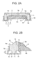
- FIG. 6A is a vertical sectional view of another conventional surface mounted crystal unit
- FIG. 6B is a transverse sectional view (partial enlargement) along the line A-A of FIG. 6A.
- an insulation base 4 that functions as a surface mounting base, comprises an annular casing wall 4a having a single through hole 7. Furthermore, a pair of lead terminals 5 is made from Cu, and is constructed such that a folded part 5d is added to a holding part 5a, a through part 5b, and a mounting terminal part 5c. A projection 10 formed on the through part 5b, and an elbow shaped part of the folded part 5d are elastically contacted with the outside and inside of the insulation base 4 (casing wall 4a).
- the lead terminal 5 is referred to as a J lead terminal that clamps the casing wall 4a (insulation base 4) (for information about J lead terminals refer to FIG. 15 and its description in http://www.lodestonepacific.com/techlib/tmappnotel.html).
- the J lead terminal 5 passes through the sealing glass 6 and clamps the inside and outside of the annular casing wall 4a (insulation base 4), and has the holding part 5a for the crystal element 2 positioned above the top surface 6a of the sealing glass 6, which is one principal surface side of the insulation base 4.
- the J lead terminal 5 is formed from the through part 5b which is embedded in the sealing glass 6, and projects from the bottom surface 6b of the sealing glass 6, the mounting terminal part (tip end part) 5c which extends from the inside of the annular casing wall 4d across the tip end surface to the outside of the annular casing wall 4a, and bends in a concave shape, and the folded part 5d.
- the J lead terminal 5 is soldered onto the insulation base 4.
- a slit 12 is provided in the center area on the through part 5b of the J lead terminal 5, and first and second bifurcated through parts 5b1 and 5b2 are formed. Moreover, the first and second bifurcated through parts 5b1 and 5b2 respectively have projections 10 that contact with the inside of the casing wall 4a (base 4).
- the tip end part (mounting terminal 5c) which is the flat bent part, pressed against the tip end surface 4b of the annular casing wall 4a (base 4)
- solid state powdered glass is filled into the single hole 7, and the sealing glass 6 is fired to integrate them.
- the J lead terminal 5 elastically clamps the inside and outside of the insulation base 4, disengagement of the J lead terminal 5 from the insulation base 4, or movement can be prevented without requiring a jig. Furthermore, since the projection 10 is provided on the through part 5b of the J lead terminal 5, a gap is created between the inside of the insulation base 4 (annular casing wall 4a) and the J lead terminal 5.
- the through part 5b of the J lead terminal 5 is constructed from the first and second bifurcated through parts 5b1 and 5b2, and the slit 12 is provided between them. Therefore, in the through hole 7, the molten glass readily enters into the gap with the inside of the casing wall 4a, from both sides of the through part 5b and from the center slit 12. As a result, manufacturing of the surface mounting base becomes easier.
- this insulation base 4a since the through hole 7 formed in this insulation base 4a is a single one, a large amount of powdered glass can be filled thereinto. Therefore, molten glass will readily enter the gap between the insulation base 4 and the lead terminal 5 at the time of melting, thus realizing an effect that manufacturing can be made even easier. This effect becomes greater when the size of the insulation base 4 is small and the amount of powdered glass to be filled is small.
- an object of the present invention is to provide a surface mounting base of enhanced compatibility, which prevents distortion when mounting a surface mounted crystal unit onto a set substrate, and to provide a highly reliable surface mounted crystal unit that uses this surface mounting base.
- the present invention is a surface mounting base for an oscillator that is provided with: an insulation base comprising a casing wall having a single through hole; a sealing glass that is filled into the through hole and forms a space part on one principal surface side of the insulation base; and a J lead terminal, which passes through the sealing glass and clamps an inner surface and an outer surface of the casing wall, and which has a holding part for a crystal element on a top surface of the sealing glass that is one principal surface side of the insulation glass, and which has a tip end part bent in a concave shape projecting from a bottom surface of the sealing glass and extending from the inside of the casing wall towards the outside across a tip end surface, and in which the tip end part is soldered to the insulation base; being a crystal unit surface mounting base provided with the J lead terminal from the bottom surface of the sealing glass, and is constructed such that a base part of the J lead terminal projects from the bottom surface of the sealing glass, and the inner surface of the tip end part is distanced from the bottom surface of the sealing glass
- the base part of the J lead terminal projects from the bottom surface of the sealing glass, and the distance from the bottom surface of the sealing glass to the tip end part of the J lead terminal can be made long. Therefore, even in the case where molten glass enters between the base part (one part of the through part) of the J lead terminal, and the casing wall of the base, the molten glass stops halfway through the base part, and does not enter between the tip end part of the J lead terminal and the tip end surface of the casing wall of the base.
- parts that do not contact with the molten glass occur in the tip end part as well as in the base part of the J lead terminal, and in particular the non-contacting part of the base part comes to function as a stress absorbing part moving freely with respect to externally applied stress.
- the tip end surface of the J lead terminal is fixed directly to the insulation base by soldering. Moreover, the free movement on the outer surface of that base part is suppressed by the solder that creeps up on it. However, since the inner surface sides of the tip end part and base part contact with neither the solder nor the sealing glass, they function sufficiently as stress absorbing parts that freely move.
- the tip end surface of the casing wall of the base projects from the bottom surface of the sealing glass.
- a projecting part is provided on the tip end surface of the casing wall, and the projecting part projects from the bottom surface of the sealing glass.
- the tip end surface of the casing wall and the tip end part of the J lead terminal are separated. According to these constructions, since the tip end part and base part of the J lead terminal that project from the bottom surface of the sealing glass contact with neither the sealing glass nor the solder, these function sufficiently as stress absorbing parts that freely move.
- the number of the through holes formed in the insulation base is just one.
- a large amount of powdered glass can be filled, and its entry between the lead terminal and the inside of the casing wall becomes excellent.
- the casing wall which is on one principal surface side of the insulation base, has a space part that holds the crystal element, which is in a position above the sealing glass. As a result, the crystal element is protected, and contact with external devices during manufacture is prevented.
- the crystal oscillator is constructed such that the holding part of the crystal element holds the periphery part of the crystal element, which has its extension electrodes extending from an excitation electrode, and a cover is placed over the surface mounting base for the crystal oscillator, to hermetically seal the crystal element.
- compatibility of the insulation base with the set substrate can be made excellent, and a highly reliable crystal oscillator can be obtained.
- FIG. 1 is a diagram for explaining a first embodiment of a surface mounted crystal unit of the present invention, wherein FIG. 1A is a vertical sectional view of the surface mounted crystal unit, FIG. 1B is a partially enlarged vertical sectional view of the surface mounted crystal unit, FIG. 1C is a plan view of the surface mounted crystal unit with the cover removed, and FIG. 1D is a perspective view of a J lead terminal of a surface mounted crystal unit of the present invention.
- a crystal element 2 is mounted on a surface mounting base 1 and is covered and hermetically sealed with a cover 3.
- the surface mounting base 1 comprises an insulation base 4 made of ceramic or the like, a sealing glass 6, and a J lead terminal 5 (refer to the description in " Background Art " for details of the J lead terminal).
- the insulation base 4 is formed from an annular casing wall 4a having a single through hole 7.
- the height of the sealing glass 6 is made lower than that of the insulation base 4 as shown in FIG. 1A, and a space part 4c for accommodating the crystal element 2 is provided on one principal surface of the sealing glass 6.
- the J lead terminal 5 is made from Cu, and has a U shape section as shown in FIG. 1A, FIG. 1B, and FIG. 1D, and comprises a holding part 5a, a through part 5b (as shown in FIG. 1D, this may be as a bifurcated through part 5b1 and 5b2), a mounting terminal part 5c, and a folded part 5d.
- the J lead terminal 5 has the holding part 5a for the crystal element 2 on a top surface 6a of the sealing glass 6, which is one principal surface of the insulation base 4 that is formed with the annular casing wall 4a.
- the through part 5b of the J lead terminal 5 projects from a bottom surface 6b of the sealing glass 6, and extends from inside of the annular casing wall 4a of the insulation base 4 across its tip end surface toward the outside of the casing wall 4a, bending in a concave shape to form the mounting terminal 5c.
- This terminal part 5c is soldered onto the insulation base 4.
- the elbow shaped folded part 5d is extended upward from the mounting terminal part (tip end part) 5c.
- the two projections 10 which face the inside of the annular casing wall 4a, are formed on the through part 5b of the lead terminal 5 as shown in FIG. 1D, and are elastically contacted with the inside in the annular casing wall 4a.
- a base part (one part of the through part 5b) of the J lead terminal 5 projects from the bottom surface 6b of the sealing glass 6 so that the inner surface of the tip end part 5c is distanced from the bottom surface 6b of the sealing glass 6.
- the tip end surface of the casing wall 4a where the J lead terminal 5 extends is made to project downward from the bottom surface 6b of the sealing glass 6.
- a distance d between the inner surface of the tip end part 5c of the J lead terminal 5 and the sealing glass 6 is at least equal to or greater than a thickness t of the J lead terminal 5.
- the thickness t of the J lead terminal 5 is 0.1 mm
- the distance d is 0.5 mm.
- a plan dimension of the insulation base (annular casing wall 4a) 4 is 5.0 x 3.2 mm and its height is 1.8 mm (excluding the thickness of the J lead terminal 5)
- a plan dimension of the sealing glass 6 is 3.8 x 2.0 mm
- the height from the bottom end of the insulation base 4 to the one principal surface (top surface) of the crystal element 2 is 1.3 mm.
- the distance d from the bottom surface 6b of the sealing glass 6 to the inner surface of the concave shaped tip end part 5c can be made long at the base part of the J lead terminal 5 which projects from the bottom surface of the sealing glass 6. Therefore, molten glass that has entered between the base part of the J lead terminal 5 and the inner surface of the annular casing wall 4a stops halfway down the base part (the through part 5b projecting from the bottom surface of the sealing glass) of the J lead terminal 5 as shown in FIG. 1B. Therefore the molten glass does not enter between the inner surface of the tip end part 5c of the J lead terminal 5 and the tip end surface 4b of the annular casing wall 4a.
- the J lead terminal 5 functions as a stress absorbing part that moves freely with respect to the sealing glass 6.
- the base part of the J lead terminal 5 extends in a vertical direction, its function as a stress absorbing part is improved.
- solder adheres directly to the tip end part 5c of the J lead terminal 5, especially on its tip end surface. Moreover, the solder that has crept up from the bottom surface adheres to the outer surface (one part of the through part 5b) of the base part. On the other hand, the flooding of solder into the inner surface of the base part and the tip end part 5c of the J lead terminal is controlled, and the J lead terminal comes to contact with neither the sealing glass 6, nor the solder. Accordingly, distortion occurring between the surface mounted crystal unit and the set substrate due to a difference in expansion coefficients is sufficiently absorbed by these stress absorbing parts.
- the base part of the J lead terminal 5 projecting from the bottom surface 6b of the sealing glass 6 becomes longer, the non-contacting area becomes greater, and the function of the stress absorbing part improves. Furthermore, since the J lead terminal is made from Cu, it sufficiently functions as a stress absorbing part due to its having flexibility (elasticity).
- solder Since solder has a greater flexibility than the sealing glass 6, the function of the stress absorbing part functions more sufficiently in the case where the tip end part 5c and the outer surface of the base part of the J lead terminal 5 are integrated with solder than in the case where the tip end part 5c and the inner surface of the base part are integrated with the sealing glass 6 by means of firing.
- the non-contacting area at the base part of the J lead terminal 5 is greater, the function as a stress absorber is improved compared to either with the sealing glass 6 or the solder.
- the space part 4c is formed between them, and the crystal element 2 is accommodated therein. Accordingly, the crystal element 2 is surrounded by the annular casing wall 4a and is not exposed from above the one principal surface of the insulation base 4. As a result, damage to the crystal element 2 can be prevented, as it does not make contact with a jig or devices and so forth in the manufacturing process of the surface mounted crystal unit.
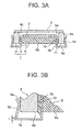
- FIG. 2 is a diagram for explaining a second embodiment of the surface mounted crystal unit of the present invention, wherein FIG. 2A is a vertical sectional view of the surface mounted crystal unit, and FIG. 2B is a partially enlarged vertical sectional view of the surface mounted crystal unit.
- the base part (part of the through part 5b) of the J lead terminal 5 projects from the bottom surface 6b of the sealing glass 6, and the inner surface of the concave shaped tip end part (mounting terminal part 5c) is distanced from the bottom surface 6b of the sealing glass 6.
- convex projecting parts 11 are symmetrically provided on opposite tip end surfaces of the annular casing wall 4a of the insulation base 4. The height d of the projecting parts 11 is at least equal to or greater than the thickness of the J lead terminal, from the bottom surface of the sealing glass 6.
- the base part of the J lead terminal 5 projects from the bottom surface 6b of the sealing glass 6, and its concaved tip end part (mounting terminal part 5c) extends from the inner surface to the outer surface across the tip end surface of the projecting part 11.
- small space parts S1 and S2 as shown in FIG. 2B are formed between the base part of the J lead terminal 5 and the insulation base 4, by the projecting part 11 provided on the tip end surface of the annular casing wall 4a. Therefore, even in the case where the J lead terminal 5 is elastically clamped on the inside and outside of the annular casing wall 4a, and the tip end part 5c is pressed against the tip end surface of the casing wall 4a, and powdered glass is sealed in and fired, due to the small space parts S1 and S2, capillary action does not occur, and molten glass does not enter further towards the tip end part 5c of the J lead terminal.
- FIG. 3 is a diagram for explaining a third embodiment of the surface mounted crystal unit of the present invention, wherein FIG. 3A is a vertical sectional view of the surface mounted crystal unit, and FIG. 3B is a partially enlarged vertical sectional view of the surface mounting base.
- the base part of the J lead terminal 5 projects from the bottom surface 6b of the sealing glass 6, and the inner surface of the tip end part (mounting terminal part 5c) is distanced from the bottom surface 6b of the sealing glass 6.
- the tip end surface of the annular casing wall 4a which is the projection side of the J lead terminal 5, and the inner surface of the tip end part of the J lead terminal 5 are distanced from each other by the thickness t of the J lead terminal, or more.
- the concave shaped tip end part 5c of the J lead terminal 5 is arranged so that it is spaced from the tip end surface 4b of the annular casing wall 4a.
- the tip end surface 4b of the annular casing wall 4a and the bottom surface 6b of the sealing glass 6 are here arranged on substantially the same plane.
- the base part of the J lead terminal 5 projects from the tip end surface 4b of the annular casing wall 4a, and from the bottom surface 6b of the sealing glass 6, which is arranged on the same plane, and the tip end part 5c of the J lead terminal 5 is distanced from the tip end surface 4b of the annular casing wall 4a. Therefore, even in the case where the J lead terminal 5 is elastically clamped on the annular casing wall 4a, and power glass is sealed into the space and fired, capillary action does not occur and molten glass does not enter into the base part and the tip end part 5c of the J lead terminal 5.
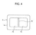
- the insulation base 4 is formed from the annular casing wall 4a, and the single through hole 7 is formed.
- a bridging part (beam) 12 may be provided over the center part of the insulation base 4 in order to enhance its strength.
- one principal surface side of the insulation base 4 has been made higher than the top surface 6a of the sealing glass 6. However, it may be arranged on the same plane as seen in the conventional example.
- the through parts 5b of the J lead terminal 5 are made into first and second bifurcated through parts 5b1 and 5b2 by having a single slit.
- a plurality of bifurcated through parts may be formed by a plurality of slits for example.
- molten glass only needs to readily enter the through part 5b.
- the slit may not be required.
- the projection 10 is provided on the through part 5b of the lead terminal 5, and the folded part 5d has an elbow shape.
- both may be made having projecting shapes or elbow shapes.
- the structure only needs to be able to elastically clamp from both surface sides of the annular casing wall 4a.
- a single through hole 7 is formed in the insulation base 4.
- a pair of through holes 7a and 7b may be provided to form an airtight terminal.
- having a single through hole 7 is more effective.
Landscapes
- Physics & Mathematics (AREA)
- Acoustics & Sound (AREA)
- Piezo-Electric Or Mechanical Vibrators, Or Delay Or Filter Circuits (AREA)
- Connections Arranged To Contact A Plurality Of Conductors (AREA)
Applications Claiming Priority (2)
| Application Number | Priority Date | Filing Date | Title |
|---|---|---|---|
| JP2004223152 | 2004-07-30 | ||
| JP2005010135A JP3837429B2 (ja) | 2004-07-30 | 2005-01-18 | 振動子用表面実装ベース及びこれを用いた水晶振動子 |
Publications (1)
| Publication Number | Publication Date |
|---|---|
| EP1622263A1 true EP1622263A1 (en) | 2006-02-01 |
Family
ID=35149397
Family Applications (1)
| Application Number | Title | Priority Date | Filing Date |
|---|---|---|---|
| EP05254717A Withdrawn EP1622263A1 (en) | 2004-07-30 | 2005-07-28 | Surface mounted crystal unit |
Country Status (4)
| Country | Link |
|---|---|
| US (1) | US7190235B2 (enExample) |
| EP (1) | EP1622263A1 (enExample) |
| JP (1) | JP3837429B2 (enExample) |
| KR (1) | KR20060048980A (enExample) |
Families Citing this family (26)
| Publication number | Priority date | Publication date | Assignee | Title |
|---|---|---|---|---|
| JP2006270944A (ja) * | 2005-02-25 | 2006-10-05 | Kyocera Corp | 圧電部品 |
| USD646236S1 (en) * | 2009-11-05 | 2011-10-04 | Seiko Instruments Inc. | Quartz crystal |
| USD643383S1 (en) * | 2009-11-06 | 2011-08-16 | Seiko Instruments Inc. | Quartz crystal |
| USD643385S1 (en) * | 2009-11-06 | 2011-08-16 | Seiko Instruments Inc. | Quartz crystal |
| USD653631S1 (en) * | 2009-11-06 | 2012-02-07 | Seiko Instruments Inc. | Quartz crystal |
| USD643382S1 (en) * | 2009-11-06 | 2011-08-16 | Seiko Instruments Inc. | Quartz crystal |
| USD634287S1 (en) * | 2009-11-06 | 2011-03-15 | Seiko Instruments Inc. | Quartz crystal |
| USD643387S1 (en) * | 2010-03-29 | 2011-08-16 | Seiko Instruments Inc. | Quartz crystal |
| USD653632S1 (en) * | 2010-03-29 | 2012-02-07 | Seiko Instruments Inc. | Quartz crystal |
| USD643384S1 (en) * | 2010-03-29 | 2011-08-16 | Seiko Instruments Inc. | Quartz crystal |
| USD646237S1 (en) * | 2010-03-29 | 2011-10-04 | Seiko Instruments Inc. | Quartz crystal |
| USD634288S1 (en) * | 2010-03-29 | 2011-03-15 | Seiko Instruments Inc. | Quartz crystal |
| USD643386S1 (en) * | 2010-03-29 | 2011-08-16 | Seiko Instruments Inc. | Quartz crystal |
| USD648288S1 (en) * | 2010-06-16 | 2011-11-08 | Seiko Instruments Inc. | Quartz crystal |
| USD646656S1 (en) * | 2010-06-16 | 2011-10-11 | Seiko Instruments Inc. | Quartz crystal |
| USD647071S1 (en) * | 2010-06-16 | 2011-10-18 | Seiko Instruments Inc. | Quartz crystal |
| USD646652S1 (en) * | 2010-06-16 | 2011-10-11 | Seiko Instruments Inc. | Quartz crystal |
| USD646655S1 (en) * | 2010-06-16 | 2011-10-11 | Seiko Instruments Inc. | Quartz crystal |
| USD646651S1 (en) * | 2010-06-16 | 2011-10-11 | Seiko Instruments Inc. | Quartz crystal |
| USD646649S1 (en) * | 2010-06-16 | 2011-10-11 | Seiko Instruments Inc. | Quartz crystal |
| USD637982S1 (en) * | 2010-06-16 | 2011-05-17 | Seiko Instruments Inc. | Quartz crystal |
| USD646654S1 (en) * | 2010-06-16 | 2011-10-11 | Seiko Instruments Inc. | Quartz crystal |
| USD646650S1 (en) * | 2010-06-16 | 2011-10-11 | Seiko Instruments Inc. | Quartz crystal |
| USD646648S1 (en) * | 2010-06-16 | 2011-10-11 | Seiko Instruments Inc. | Quartz crystal |
| USD646653S1 (en) * | 2010-06-16 | 2011-10-11 | Seiko Instruments Inc. | Quartz crystal |
| EP2806772A4 (en) * | 2012-01-24 | 2015-09-09 | Bunn O Matic Corp | brewing |
Citations (5)
| Publication number | Priority date | Publication date | Assignee | Title |
|---|---|---|---|---|
| JPH08279725A (ja) * | 1995-04-05 | 1996-10-22 | Nec Kansai Ltd | 表面実装型セラミックパッケージ |
| JPH1131939A (ja) * | 1997-07-14 | 1999-02-02 | Matsushita Electric Ind Co Ltd | 表面実装型水晶振動子およびその製造方法 |
| JPH11103231A (ja) * | 1997-09-26 | 1999-04-13 | Citizen Electronics Co Ltd | 圧電振動子とその製造方法 |
| JP2000286661A (ja) * | 1999-03-31 | 2000-10-13 | Kinseki Ltd | 表面実装型電子部品 |
| JP2003297453A (ja) | 2002-03-29 | 2003-10-17 | Matsushita Electric Ind Co Ltd | 表面実装型気密端子とそれを用いた水晶振動子 |
Family Cites Families (2)
| Publication number | Priority date | Publication date | Assignee | Title |
|---|---|---|---|---|
| JP3980954B2 (ja) * | 2002-07-15 | 2007-09-26 | 日本電波工業株式会社 | 表面実装水晶発振器 |
| US7076870B2 (en) * | 2004-08-16 | 2006-07-18 | Pericom Semiconductor Corp. | Manufacturing process for a surface-mount metal-cavity package for an oscillator crystal blank |
-
2005
- 2005-01-18 JP JP2005010135A patent/JP3837429B2/ja not_active Expired - Fee Related
- 2005-07-25 US US11/188,414 patent/US7190235B2/en not_active Expired - Fee Related
- 2005-07-28 EP EP05254717A patent/EP1622263A1/en not_active Withdrawn
- 2005-07-29 KR KR1020050069936A patent/KR20060048980A/ko not_active Withdrawn
Patent Citations (5)
| Publication number | Priority date | Publication date | Assignee | Title |
|---|---|---|---|---|
| JPH08279725A (ja) * | 1995-04-05 | 1996-10-22 | Nec Kansai Ltd | 表面実装型セラミックパッケージ |
| JPH1131939A (ja) * | 1997-07-14 | 1999-02-02 | Matsushita Electric Ind Co Ltd | 表面実装型水晶振動子およびその製造方法 |
| JPH11103231A (ja) * | 1997-09-26 | 1999-04-13 | Citizen Electronics Co Ltd | 圧電振動子とその製造方法 |
| JP2000286661A (ja) * | 1999-03-31 | 2000-10-13 | Kinseki Ltd | 表面実装型電子部品 |
| JP2003297453A (ja) | 2002-03-29 | 2003-10-17 | Matsushita Electric Ind Co Ltd | 表面実装型気密端子とそれを用いた水晶振動子 |
Non-Patent Citations (5)
| Title |
|---|
| PATENT ABSTRACTS OF JAPAN vol. 1997, no. 02 28 February 1997 (1997-02-28) * |
| PATENT ABSTRACTS OF JAPAN vol. 1999, no. 05 31 May 1999 (1999-05-31) * |
| PATENT ABSTRACTS OF JAPAN vol. 1999, no. 09 30 July 1999 (1999-07-30) * |
| PATENT ABSTRACTS OF JAPAN vol. 2000, no. 13 5 February 2001 (2001-02-05) * |
| PATENT ABSTRACTS OF JAPAN vol. 2003, no. 12 5 December 2003 (2003-12-05) * |
Also Published As
| Publication number | Publication date |
|---|---|
| KR20060048980A (ko) | 2006-05-18 |
| US7190235B2 (en) | 2007-03-13 |
| US20060022557A1 (en) | 2006-02-02 |
| JP3837429B2 (ja) | 2006-10-25 |
| JP2006066377A (ja) | 2006-03-09 |
Similar Documents
| Publication | Publication Date | Title |
|---|---|---|
| US7190235B2 (en) | Surface mounted crystal unit | |
| KR101117049B1 (ko) | 기밀 밀봉용 캡 및 그 제조 방법 | |
| US20080079505A1 (en) | Surface mounting piezoelectric oscillator | |
| JP3996904B2 (ja) | 電子素子用の表面実装ベース | |
| JPH06260582A (ja) | 半導体装置 | |
| CN100525095C (zh) | 表面安装晶体单元 | |
| JP2009105776A (ja) | 表面実装用の水晶デバイス | |
| JP4890914B2 (ja) | 水晶振動片の支持部構造 | |
| JP4364537B2 (ja) | チップ型圧電振動子 | |
| JP4373309B2 (ja) | 電子部品用パッケージ | |
| JP5101093B2 (ja) | 圧電発振器及びその製造方法 | |
| JP2006060106A (ja) | リード部材及び表面実装型半導体装置 | |
| JP2001028407A (ja) | 光半導体素子収納用パッケージ | |
| JP4731232B2 (ja) | 電子素子用の表面実装ベース | |
| JP4585847B2 (ja) | 水晶発振器及びその製造方法 | |
| JP5400634B2 (ja) | 圧電発振器 | |
| JP2001060842A (ja) | 小型電子部品 | |
| JP2008187751A (ja) | 表面実装型圧電発振器 | |
| JP2006041068A (ja) | 横置き型面実装電解コンデンサ | |
| JP4370616B2 (ja) | 表面実装型電子部品 | |
| JP2008166525A (ja) | 電子回路モジュール | |
| JP2005167508A (ja) | 圧電発振器 | |
| JP2000165180A (ja) | 表面実装用容器及び水晶振動子 | |
| JP2003023335A (ja) | 圧電振動子 | |
| JP2007036808A (ja) | 圧電発振器 |
Legal Events
| Date | Code | Title | Description |
|---|---|---|---|
| PUAI | Public reference made under article 153(3) epc to a published international application that has entered the european phase |
Free format text: ORIGINAL CODE: 0009012 |
|
| AK | Designated contracting states |
Kind code of ref document: A1 Designated state(s): AT BE BG CH CY CZ DE DK EE ES FI FR GB GR HU IE IS IT LI LT LU LV MC NL PL PT RO SE SI SK TR |
|
| AX | Request for extension of the european patent |
Extension state: AL BA HR MK YU |
|
| 17P | Request for examination filed |
Effective date: 20060720 |
|
| 17Q | First examination report despatched |
Effective date: 20060822 |
|
| AKX | Designation fees paid |
Designated state(s): AT BE BG CH CY CZ DE DK EE ES FI FR GB GR HU IE IS IT LI LT LU LV MC NL PL PT RO SE SI SK TR |
|
| GRAP | Despatch of communication of intention to grant a patent |
Free format text: ORIGINAL CODE: EPIDOSNIGR1 |
|
| STAA | Information on the status of an ep patent application or granted ep patent |
Free format text: STATUS: THE APPLICATION IS DEEMED TO BE WITHDRAWN |
|
| 18D | Application deemed to be withdrawn |
Effective date: 20110728 |