EP1619725A2 - Dispositif semiconducteur à couche mince et son procédé de fabrication, dispositif électro-optique et appareil électronique - Google Patents
Dispositif semiconducteur à couche mince et son procédé de fabrication, dispositif électro-optique et appareil électronique Download PDFInfo
- Publication number
- EP1619725A2 EP1619725A2 EP05013531A EP05013531A EP1619725A2 EP 1619725 A2 EP1619725 A2 EP 1619725A2 EP 05013531 A EP05013531 A EP 05013531A EP 05013531 A EP05013531 A EP 05013531A EP 1619725 A2 EP1619725 A2 EP 1619725A2
- Authority
- EP
- European Patent Office
- Prior art keywords
- layer
- protective circuit
- semiconductor
- thin film
- film
- Prior art date
- Legal status (The legal status is an assumption and is not a legal conclusion. Google has not performed a legal analysis and makes no representation as to the accuracy of the status listed.)
- Withdrawn
Links
- 239000004065 semiconductor Substances 0.000 title claims abstract description 183
- 239000010409 thin film Substances 0.000 title claims abstract description 92
- 238000004519 manufacturing process Methods 0.000 title claims description 22
- 230000001681 protective effect Effects 0.000 claims abstract description 151
- 239000010408 film Substances 0.000 claims abstract description 147
- 239000000758 substrate Substances 0.000 claims abstract description 51
- 239000012535 impurity Substances 0.000 claims description 44
- 238000000034 method Methods 0.000 claims description 29
- 239000010410 layer Substances 0.000 description 88
- 239000004973 liquid crystal related substance Substances 0.000 description 22
- 238000010586 diagram Methods 0.000 description 9
- 229910052751 metal Inorganic materials 0.000 description 5
- 239000002184 metal Substances 0.000 description 5
- 230000005611 electricity Effects 0.000 description 4
- 230000003068 static effect Effects 0.000 description 4
- 230000015572 biosynthetic process Effects 0.000 description 3
- 239000000470 constituent Substances 0.000 description 3
- 239000003990 capacitor Substances 0.000 description 2
- 239000000969 carrier Substances 0.000 description 2
- 230000015556 catabolic process Effects 0.000 description 2
- 230000001413 cellular effect Effects 0.000 description 2
- 230000000694 effects Effects 0.000 description 2
- 230000005684 electric field Effects 0.000 description 2
- 238000009413 insulation Methods 0.000 description 2
- 239000011229 interlayer Substances 0.000 description 2
- 239000011159 matrix material Substances 0.000 description 2
- 229920002120 photoresistant polymer Polymers 0.000 description 2
- 229910021420 polycrystalline silicon Inorganic materials 0.000 description 2
- 229920005591 polysilicon Polymers 0.000 description 2
- 239000000565 sealant Substances 0.000 description 2
- ZOKXTWBITQBERF-UHFFFAOYSA-N Molybdenum Chemical compound [Mo] ZOKXTWBITQBERF-UHFFFAOYSA-N 0.000 description 1
- VYPSYNLAJGMNEJ-UHFFFAOYSA-N Silicium dioxide Chemical compound O=[Si]=O VYPSYNLAJGMNEJ-UHFFFAOYSA-N 0.000 description 1
- 229910052782 aluminium Inorganic materials 0.000 description 1
- XAGFODPZIPBFFR-UHFFFAOYSA-N aluminium Chemical compound [Al] XAGFODPZIPBFFR-UHFFFAOYSA-N 0.000 description 1
- 230000005540 biological transmission Effects 0.000 description 1
- 238000010276 construction Methods 0.000 description 1
- 238000006731 degradation reaction Methods 0.000 description 1
- 239000007943 implant Substances 0.000 description 1
- 239000012212 insulator Substances 0.000 description 1
- 229910052750 molybdenum Inorganic materials 0.000 description 1
- 239000011733 molybdenum Substances 0.000 description 1
- 230000002093 peripheral effect Effects 0.000 description 1
- 229910052814 silicon oxide Inorganic materials 0.000 description 1
- 229910052715 tantalum Inorganic materials 0.000 description 1
- GUVRBAGPIYLISA-UHFFFAOYSA-N tantalum atom Chemical compound [Ta] GUVRBAGPIYLISA-UHFFFAOYSA-N 0.000 description 1
Images


Classifications
-
- G—PHYSICS
- G02—OPTICS
- G02F—OPTICAL DEVICES OR ARRANGEMENTS FOR THE CONTROL OF LIGHT BY MODIFICATION OF THE OPTICAL PROPERTIES OF THE MEDIA OF THE ELEMENTS INVOLVED THEREIN; NON-LINEAR OPTICS; FREQUENCY-CHANGING OF LIGHT; OPTICAL LOGIC ELEMENTS; OPTICAL ANALOGUE/DIGITAL CONVERTERS
- G02F1/00—Devices or arrangements for the control of the intensity, colour, phase, polarisation or direction of light arriving from an independent light source, e.g. switching, gating or modulating; Non-linear optics
- G02F1/01—Devices or arrangements for the control of the intensity, colour, phase, polarisation or direction of light arriving from an independent light source, e.g. switching, gating or modulating; Non-linear optics for the control of the intensity, phase, polarisation or colour
- G02F1/13—Devices or arrangements for the control of the intensity, colour, phase, polarisation or direction of light arriving from an independent light source, e.g. switching, gating or modulating; Non-linear optics for the control of the intensity, phase, polarisation or colour based on liquid crystals, e.g. single liquid crystal display cells
- G02F1/133—Constructional arrangements; Operation of liquid crystal cells; Circuit arrangements
- G02F1/136—Liquid crystal cells structurally associated with a semi-conducting layer or substrate, e.g. cells forming part of an integrated circuit
- G02F1/1362—Active matrix addressed cells
- G02F1/136204—Arrangements to prevent high voltage or static electricity failures
-
- H—ELECTRICITY
- H01—ELECTRIC ELEMENTS
- H01L—SEMICONDUCTOR DEVICES NOT COVERED BY CLASS H10
- H01L27/00—Devices consisting of a plurality of semiconductor or other solid-state components formed in or on a common substrate
- H01L27/02—Devices consisting of a plurality of semiconductor or other solid-state components formed in or on a common substrate including semiconductor components specially adapted for rectifying, oscillating, amplifying or switching and having at least one potential-jump barrier or surface barrier; including integrated passive circuit elements with at least one potential-jump barrier or surface barrier
- H01L27/0203—Particular design considerations for integrated circuits
- H01L27/0248—Particular design considerations for integrated circuits for electrical or thermal protection, e.g. electrostatic discharge [ESD] protection
- H01L27/0251—Particular design considerations for integrated circuits for electrical or thermal protection, e.g. electrostatic discharge [ESD] protection for MOS devices
- H01L27/0255—Particular design considerations for integrated circuits for electrical or thermal protection, e.g. electrostatic discharge [ESD] protection for MOS devices using diodes as protective elements
-
- H—ELECTRICITY
- H01—ELECTRIC ELEMENTS
- H01L—SEMICONDUCTOR DEVICES NOT COVERED BY CLASS H10
- H01L27/00—Devices consisting of a plurality of semiconductor or other solid-state components formed in or on a common substrate
- H01L27/02—Devices consisting of a plurality of semiconductor or other solid-state components formed in or on a common substrate including semiconductor components specially adapted for rectifying, oscillating, amplifying or switching and having at least one potential-jump barrier or surface barrier; including integrated passive circuit elements with at least one potential-jump barrier or surface barrier
- H01L27/12—Devices consisting of a plurality of semiconductor or other solid-state components formed in or on a common substrate including semiconductor components specially adapted for rectifying, oscillating, amplifying or switching and having at least one potential-jump barrier or surface barrier; including integrated passive circuit elements with at least one potential-jump barrier or surface barrier the substrate being other than a semiconductor body, e.g. an insulating body
-
- H—ELECTRICITY
- H01—ELECTRIC ELEMENTS
- H01L—SEMICONDUCTOR DEVICES NOT COVERED BY CLASS H10
- H01L29/00—Semiconductor devices adapted for rectifying, amplifying, oscillating or switching, or capacitors or resistors with at least one potential-jump barrier or surface barrier, e.g. PN junction depletion layer or carrier concentration layer; Details of semiconductor bodies or of electrodes thereof ; Multistep manufacturing processes therefor
- H01L29/66—Types of semiconductor device ; Multistep manufacturing processes therefor
- H01L29/68—Types of semiconductor device ; Multistep manufacturing processes therefor controllable by only the electric current supplied, or only the electric potential applied, to an electrode which does not carry the current to be rectified, amplified or switched
- H01L29/70—Bipolar devices
- H01L29/72—Transistor-type devices, i.e. able to continuously respond to applied control signals
- H01L29/739—Transistor-type devices, i.e. able to continuously respond to applied control signals controlled by field-effect, e.g. bipolar static induction transistors [BSIT]
- H01L29/7391—Gated diode structures
-
- H—ELECTRICITY
- H01—ELECTRIC ELEMENTS
- H01L—SEMICONDUCTOR DEVICES NOT COVERED BY CLASS H10
- H01L29/00—Semiconductor devices adapted for rectifying, amplifying, oscillating or switching, or capacitors or resistors with at least one potential-jump barrier or surface barrier, e.g. PN junction depletion layer or carrier concentration layer; Details of semiconductor bodies or of electrodes thereof ; Multistep manufacturing processes therefor
- H01L29/66—Types of semiconductor device ; Multistep manufacturing processes therefor
- H01L29/86—Types of semiconductor device ; Multistep manufacturing processes therefor controllable only by variation of the electric current supplied, or only the electric potential applied, to one or more of the electrodes carrying the current to be rectified, amplified, oscillated or switched
- H01L29/861—Diodes
- H01L29/868—PIN diodes
Definitions
- the present invention relates to a thin film semiconductor device, to a method of manufacturing the same, to an electro-optical device, and to an electronic apparatus.
- semiconductor integrated circuit devices or active-matrix-type electro-optical devices include a protective circuit for protecting internal circuits from static electricity.
- the electro-optical devices have a protective circuit disposed between internal circuits, such as a pixel switching element and a driving circuit, and a pad for drawing an electrode.
- the semiconductor integrated circuit devices use a diode as a protective circuit.
- the electro-optical devices use a diode-connected thin film transistor (hereinafter, referred to as a TFT).
- FIG. 9A is a diagram showing the structure of a protective circuit using a diode-connected TFT
- FIG. 9B is a cross-sectional view schematically showing the diode-connected TFT.
- two resistive elements R1 and R2 are interposed between a connection pad 219 and an internal circuit 217.
- Two diode-connected TFTs 30D are disposed along a path that connects connection pads 219b (Vdd) and 219c (Vss) between the resistive elements R1 and R2.
- Vdd connection pads 219b
- Vss 219c
- the diode-connected TFT 30D includes a semiconductor film 201 formed on a substrate 211, a gate electrode 213a disposed opposite to the semiconductor film 201 with a gate insulating film 212 interposed therebetween, and a source electrode 208 and a drain electrode 209, which are connected to the semiconductor film 201 through contact holes formed in the insulating films 212 and 216. Further, the drain electrode 209 and a connection electrode 213d connected to the gate electrode 213a through a contact hole formed in the insulating film 216 are short-circuited, thereby forming a TFT having the diode-connected structure.
- a positive surge voltage such as static electricity
- a current i flows through the diode-connected TFT 30D, thereby preventing an excessive current from flowing through the internal circuit 217.
- the protective circuit can be formed using the same process as the TFTs constituting an internal circuit.
- the electrical charge penetrates the gate insulating film 212, which is a thin insulating film, of the diode-connected TFT 30D, thus forming a short-circuit path bd.
- the gate electrode 213a is electrically connected to the source region 201b of the semiconductor film 201 through the short-circuit path bd.
- connection pads 219 shown in FIG. 9A and other connection pads 219b to 219c are electrically connected to each other, and the connection pad 219a cannot operate in a normal manner. This leads to problems in the semiconductor device.
- An advantage of the invention is that it provides a thin film semiconductor device having a protective circuit element for effectively protecting an internal circuit from a surge voltage with excellent reliability, whereby problems do not occur in the circuit structure even if the protective circuit is broken due to an excessive voltage, and a method of manufacturing the same.
- a thin film semiconductor device including a substrate, a semiconductor film formed on the substrate, and a protective circuit element that includes a PIN diode having the semiconductor film and a floating electrode disposed opposite to an I layer of the PIN diode with an insulating film interposed therebetween.
- the PIN diode is a diode having a semiconductor film in which a P layer (a P-type semiconductor layer), an I layer (an intrinsic semiconductor layer or a semiconductor layer into which an impurity of a low concentration is implanted), and an N layer (a N-type semiconductor layer) are defined, as well known.
- the floating electrode is an electrode, which is not connected to electrically controlled conductive films or a constituting member of a semiconductor layer, but is in an electrically 'floated' state.
- the protective circuit element provided in the thin film semiconductor device of the invention includes the PIN diode and the floating electrode disposed opposite to the I layer. Therefore, in a case in which the excessive current flows through the protective circuit element and the gate insulating film is broken and in an electrically conductive state, the P layer (or the N layer) of the PIN diode and the floating electrode are adapted to be short-circuited from each other. Since the floating electrode is not connected to the electrically controlled conductive layers or the semiconductor layer, it is possible to secure the insulation of the PIN diode even after the protective circuit element is broken. Therefore, if a protective circuit is constructed using the protective circuit element, an electrostatic protective circuit that can bypass the surge voltage due to static electricity, etc., can be constructed. It is also possible to provide a thin film semiconductor device that can normally operate even after the surge voltage that can break the protective circuit element is input.
- the thin film semiconductor device can have a protection function even against the surge voltage of a backward direction, which may have a bad influence on a TFT device, if it is a little.
- a thin film semiconductor device including a main circuit unit having a semiconductor element, a terminal unit extending from the main circuit unit, and a protective circuit unit disposed between the main circuit unit and the terminal unit, all of which are formed on a substrate.
- the protective circuit unit can a protective circuit element that includes a PIN diode having the semiconductor film, and a floating electrode disposed opposite to an I layer of the PIN diode with an insulating film interposed therebetween.
- the protective circuit element is adapted to secure the insulation of a PIN diode itself even when it is broken due to excessive current. For this reason, if the protective circuit unit having the protective circuit element is provided, the circuit structure that connects a terminal unit and a main circuit unit is not changed although the protective circuit element is broken due to the excessive surge current input from the terminal unit, unlike the protective circuit element made of the diode-connected TFT of the related art. Therefore, the invention can provide a thin film semiconductor device, which has high the reliability and a long life span and can normally operate even after the surge voltage that can break a protective circuit element is input.
- the semiconductor film constituting the PIN diode and a semiconductor film constituting the semiconductor element of the main circuit unit be a semiconductor film formed in the same layer on the substrate. According to this construction, the semiconductor element of the main circuit unit and the PIN diode can be formed in the same process. It is thus possible to improve the reliability of a thin film semiconductor device without changing a manufacturing process.
- the semiconductor element provided in the main circuit unit be a thin film transistor, and a conductive film constituting the floating electrode and a conductive film constituting a gate electrode of the thin film transistor be formed in the same layer on the substrate. According to the structure, there is an advantage in that the thin film transistor of the main circuit unit and the protective circuit element can be formed in the same process.
- the floating electrode and the I layer of the PIN diode be formed approximately at the same location in plan view.
- the I layer of the PIN diode can be formed in a self-aligned manner by introducing an impurity into a semiconductor film using a floating electrode as a mask.
- a protective circuit element can be fabricated by means of a simple process.
- an I layer of a PIN diode can be simultaneously formed at the same time through a process of forming a channel region in a self-aligned manner using a gate electrode of the thin film transistor as a mask. This results in a thin film semiconductor device with excellent manufacturing efficiency.
- a PIN diode In the thin film semiconductor device, it is preferable that a PIN diode have a low concentration impurity region, which has an impurity concentration lower than that of a P layer or a N layer, between the P layer and the I layer or the N layer and the I layer.
- a thin film transistor provided in a thin film semiconductor device frequently adopts the LDD (Lightly Doped Drain) structure in order to prevent degradation of electrical characteristics due to hot carriers.
- LDD Lightly Doped Drain
- a manufacturing process can be standardized in the case in which a protective circuit element is formed at the same time as the thin film transistor of the LDD structure.
- the withstand voltage of the PIN diode can further increase even in terms of electrical characteristics, and the protective circuit element with high reliability can be provided.
- the low concentration impurity region be formed in a region where it overlaps a floating electrode in plan view. If this structure is adopted, although the thin film transistor of the main circuit unit has the GOLDD (gate overlapped lightly doped drain) structure, the manufacturing process can be standardized and the withstand voltage of a PIN diode can further increase.
- GOLDD gate overlapped lightly doped drain
- the floating electrode disposed opposite to the I layer of the PIN diode with the insulating film interposed therebetween have a portion in which the floating electrode overlap some of the P layer or the N layer of the PIN diode in plan view.
- the main circuit and the protective circuit element can be fabricated by means of a common manufacturing process, and can also be fabricated by a separate process. As such, although a manufacturing process is different according to the situation, the same electrical characteristics of the protective circuit element as that described above can be obtained.
- the protective circuit element be directly connected to the terminal unit.
- a resistive element R1 is disposed between a connection pad 219a and a diode-connected TFT 30D.
- the resistive element R1 is an element usually having a N-type or a P-type semiconductor layer, but has a function of prohibiting the abrupt voltage rise due to the surge voltage inputted from a connection pad 219a, thereby protecting a diode-connected TFT 30D.
- a power supply line Vdd or Vss serves to directly prevent a short circuit with a connection pad 219a.
- the pad 219a becomes rarely short with Vdd or Vss of the power supply line even when the protective circuit element is broken, as described above. It is thus possible to secure the electrical connection between the terminal unit and the main circuit unit.
- the resistive element is disposed between the protective circuit element and the terminal unit, it can be broken when the input surge voltage is excessively high. Therefore, since the terminal unit and the internal circuit are disconnected, the thin film semiconductor device does not normally operate. Therefore, if the structure in which the protective circuit element and the terminal unit are directly connected is adopted, the thin film semiconductor device can guarantee the normal operation of the main circuit unit even if the voltage that can break the protective circuit unit is inputted.
- a method of manufacturing a thin film semiconductor device having a substrate and a semiconductor film formed on the substrate includes forming a protective circuit element.
- the forming of a protective circuit element includes forming a semiconductor film on a substrate, forming an insulating film on the semiconductor film, forming a conductive film on the insulating film, forming a floating electrode that overlaps the semiconductor film in plan view, and forming a P layer, an N layer, and an I layer in the semiconductor film by introducing an impurity into the semiconductor film using the floating electrode as a mask and forming a PIN diode.
- each layer of a PIN diode can be formed by introducing an impurity into a semiconductor film using the floating electrode as a mask. It is therefore possible to form a protective circuit element with excellent reliability in an efficient manner, and thus to manufacture a thin film semiconductor device with excellent reliability with easy and efficiency.
- a method of manufacturing a thin film semiconductor device including a main circuit unit having a semiconductor element, a terminal unit extending from the main circuit unit, and a protective circuit unit disposed between the main circuit unit and the terminal unit, all of which are formed on a substrate, the method includes forming the protective circuit unit which includes forming of a protective circuit element.
- the thin film semiconductor device includes an external connection terminal. It is possible to fabricate a thin film semiconductor device in a convenient and efficient manner, which can advantageously protect a main circuit unit from the surge voltage input from a terminal unit.
- the main circuit unit include a thin film transistor having a semiconductor film, and a gate electrode opposite to the semiconductor film with an insulating film interposed therebetween. It is preferable that the semiconductor film constituting the thin film transistor and a semiconductor film constituting the protective circuit element be formed in the same process, and the gate electrode constituting the thin film transistor and the floating electrode constituting the protective circuit element be formed in the same process. Further, it is preferable that a source or drain of the thin film transistor, and the P layer or the N layer of the PIN diode is preferably formed in the same impurity introducing process.
- a thin film transistor constituting a main circuit unit and a protective circuit element can be fabricated in the same process. It is thus possible to fabricate a thin film semiconductor device with excellent reliability without changing a manufacturing process.
- a low concentration impurity region having a lower impurity concentration than that of a neighboring impurity introduction region be formed in the semiconductor film of the thin film transistor and the semiconductor film of the protective circuit element. Therefore, a thin film transistor having the LDD structure, and a protective circuit element including a structure of the withstand voltage higher than that of the above-mentioned PIN diode can be formed in the same process.
- an electro-optical device having the above-mentioned thin film semiconductor device.
- the thin film semiconductor device can be used as a TFT array substrate of an active-matrix-type electro-optical device.
- a TFT is used as a switching element of a pixel, which constitutes an image display area.
- An inverter using a TFT is also formed in a driving circuit disposed in a frame region. Further, a terminal unit serving as an external connection terminal is disposed. If the above-mentioned structure is applied to such a TFT array substrate, the switching element or the driving circuit of the image display area constituting an internal circuit can be advantageously protected by means of the protective circuit unit. It is thus possible to construct electro-optical devices having excellent reliability and a long life span.
- an electronic apparatus including the above-mentioned electro-optical device.
- the electronic apparatus includes a protective circuit, which can advantageously protect an internal circuit from the excessive voltage such as the surge voltage. It is therefore possible to construct electronic apparatuses having a display unit of excellent reliability and a long life span.
- FIG. 1 is a diagram showing the structure of a thin film semiconductor device according to a first embodiment of the invention.
- the thin film semiconductor device according to the present embodiment includes an internal circuit (a main circuit unit) 17, a protective circuit unit 18, and a terminal unit 19.
- the terminal unit 19 includes a plurality of connection pads 19a to 19c.
- the protective circuit unit 18 is interposed between the connection pads 19a to 19c, and the internal circuit 17.
- the connection pads 19b and 19c are power input terminals (Vdd and Vss).
- the protective circuit unit 18 includes a plurality of protective circuit elements 181 and 182 which are connected in series to each other.
- a signal wiring line 23 extending from the connection pad 19a is connected between the two protective circuit elements 181 and 182 with a resistive element 18b therebetween.
- a signal wiring line 24 extending from the internal circuit 17 is connected to the protective circuit elements 181 and 182 and the signal wiring line 23, with a resistive element 18c interposed between the signal wiring line 23 and the signal wiring line 24.
- the protective circuit element 181 has one end (the cathode side) connected to the connection pad 19b (Vdd) serving as the power input terminal through a signal wiring line, and the protective circuit element 182 has another end (the anode side) connected to the connection pad 19c (Vss) through a signal wiring line.
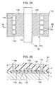
- FIG. 2A is a plan view showing the detailed structure of the protective circuit element 181 shown in FIG. 1, and FIG. 2B is a cross-sectional view of the protective circuit element taken along the line II-II in FIG. 2A.
- FIG. 2 shows only essential elements of the protective circuit element 181, except for wiring lines connected thereto, etc. Further, it should be noted that the protective circuit element 182 has the same structure as the protective circuit element 181.
- the protective circuit element 181 includes a PIN diode 181a, and a floating electrode 118g disposed to overlap a part of the PIN diode 181a.
- the PIN diode 181a includes a semiconductor film 118s, and a plurality (e.g., four in the drawing) of anode electrodes 118a and a plurality (e.g., four in the drawing) of cathode electrodes 118c connected to the semiconductor film 118s.
- the semiconductor film 118s includes a P layer 118p, an N layer 118n, and an I layer 118i disposed between the P layer 118p and the N layer 118n.
- the anode electrodes 118a are electrically connected to the P layer 118p.
- the cathode electrodes 118c are electrically connected to the N layer 118n.
- the floating electrode 118g is disposed in the I layer 118i of the PIN diode 181a in an opposite manner.
- the cross-sectional structure of the protective circuit element will now be described with reference to FIG. 2B.
- the semiconductor film 118s formed of, for example, a polysilicon film, is formed on a substrate 11.
- a first insulating film 2 formed of, for example, silicon oxide, is formed to cover the semiconductor film 118s.
- a second insulating film 6 is formed to cover the floating electrode 118g.
- anode electrode 118a and the cathode electrode 118c are buried in contact holes, which penetrate the second insulating film 6 and the first insulating film 2 to reach the semiconductor film 118s, and are then electrically connected to the P layer 118p and the N layer 118n, respectively.
- the floating electrode 118g formed in the thin film semiconductor element 181 is composed of a conductive film that is buried between the first insulating film 2 and the second insulating film 6, as shown in FIG. 2B.
- the floating electrode 118g is an electrode that is not electrically connected to other elements, is not connected to a ground, and has the predetermined voltage.
- the internal circuit 17 shown in FIG. 1 includes a semiconductor element that is formed using a thin semiconductor film formed on the substrate 11, in the same manner as the protective circuit unit 18.
- the internal circuit 17 can include, for example, a TFT (thin film transistor).
- the protective circuit unit 18 having the thin film semiconductor element 181 can effectively protect the internal circuit 17 from a positive surge voltage, such as static electricity, which is inputted through, e.g., the connection pad 19a. That is, if the surge voltage is inputted from the connection pad 19a, a current flows between the PIN diodes 181 and 182, whereby the surge current bypasses toward the power input terminal. It is thus possible to prevent an excessive current from flowing through the internal circuit 17.
- a positive surge voltage such as static electricity
- the thin film semiconductor device of the present embodiment has an advantage that cannot be obtained through the protective circuit according to the related art using the diode-connected TFT in that a problem does not occur in the electrical connection structure with the internal circuit 17 and the connection pad 19a even if the protective circuit elements 181 and 182 are broken due to the surge voltage exceeding the withstand voltage.
- the protective circuit element 181 shown in FIG. 2 As an example.
- the first insulating film 2 made of a thin insulating film is deteriorated due to the electrical charge in the same manner as a diode-connected TFT 30D shown in FIG. 9.
- This may make cause the P layer 118p (or the N layer 118n) of the PIN diode 181a and the floating electrode 118g to be short-circuited.
- the diode-connected TFT 30D according to the related art becomes conductive.
- the P layer 118p and the floating electrode 118g are short-circuited, but the floating electrode 118g is not electrically connected to the other constituent elements.
- the anode electrode 118a and the cathode electrode 118c of the PIN diode 181a are not short-circuited. Therefore, after breakage, the protective circuit element 181 serves as a simple insulator. As such, since the circuit structure connecting the connection pad 19a and the internal circuit 17 remains intact, the circuit can normally operate without causing a problem in the thin film semiconductor device, even if the surge voltage exceeding the withstand voltage of the protective circuit is inputted.
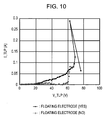
- FIG. 10 shows the results of measuring TLP (Transmission Line Pulse) characteristics of a PIN diode depending upon whether a floating electrode exists or not.
- TLP Transmission Line Pulse
- the horizontal axis indicates the load voltage in the reverse direction applied to a protective circuit element
- the vertical axis indicates the current flowing through the protective circuit element in this case.
- the solid line corresponds to a case in which the floating electrode exists
- the broken line corresponds to a case in which the floating electrode does not exist. From FIG.
- the graph showing the diode having the floating electrode has a gradient greater than that of the diode not having the floating electrode, in a region where the load voltage exceeds 20 V. Accordingly, the present embodiment is characterized in that the current flows even in a relatively low load voltage region even against a voltage in the reverse direction. Therefore, it is possible to form a protective circuit that can form a bypass for the low surge voltage in the reverse direction as well as the forward direction by using the protection element of the present embodiment. As such, the protective circuit element of the invention can have excellent protection performance as a protective element for both polarities.
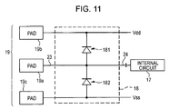
- the thin film semiconductor device having the protective circuit unit 18 showing the above effect can have a structure in which the protective circuit elements 181 and 182, and the connection pad 19a are directly connected through the wiring line 23 without forming the resistive element 18b shown in FIG. 1, as shown in FIG. 11.
- the resistive element 18b serves to protect the circuit by suppressing a rapid rise of the voltage in the circuit when the surge voltage is inputted from the connection pad 19a.
- the resistive element 18b can also be broken, which causing disconnection. If the resistive element 18b is disconnected, the connection pad 19a and the internal circuit 17 are disconnected, thus causing a problem in the operation of the thin film semiconductor device.
- the connection pad 19a and the internal circuit 17 can be still electrically connected to each other even when the protective circuit element is broken due to the excessive surge voltage. Therefore, since there is no possibility that the thin film semiconductor device itself may not operate due to the breakage of the protective circuit unit 18, the life span of the thin film semiconductor device can be improved.
- the thin film semiconductor device according to the above-mentioned embodiment can be constructed as an active-matrix-type electro-optical device.
- an active-matrix-type transmissive liquid crystal display device will be described as an example of the electro-optical device having the thin film semiconductor device shown in FIG. 1.
- FIG. 3A is a plan view of the liquid crystal display device according to the present embodiment, which is viewed from the side of the counter substrate together with the respective constituent elements.
- FIG. 3B is a cross-sectional view of the liquid crystal display device taken along the line III-III in FIG. 3A. Further, in the drawings used for the following description, the scale of each layer or member is adjusted in order to have a recognizable size in the drawings.
- the liquid crystal display device 10 has a structure in which a TFT array substrate 11 (a base substrate) and an counter substrate 12, each made of a transparent substrate, are bonded by sealants 13, and a liquid crystal layer 14 is sealed within a space defined by the sealant 13, as shown in FIGS. 3A and 3B.
- An image display area 17c is formed approximately at the center of the TFT array substrate 11.
- a data line driving circuit 17a is disposed at an area that extends along one side (a side extending in an X direction in FIG. 3) of the TFT array substrate 11.
- the data line driving circuit 17a is composed of unit circuits (not shown) in the same number as the number of pixels of the image display area 17c in the X direction.
- two scanning line driving circuits 17b are respectively formed at both sides of the image display area 17c along two short sides (sides extending in a Y direction in FIG. 3A) of the TFT array substrate 11.
- a plurality of wiring lines 22, which connects the two scanning line driving circuits 17b and 17b disposed at both sides of the image display area 17c, are provided at the one remaining side of the TFT array substrate 11.
- connection pads 19a for connecting an FPC (Flexible Printed Circuit) to the corresponding TFT array substrate 11 are disposed near one end of the data line driving circuit 17a of the TFT array substrate 11 at a predetermined pitch in the X direction.
- a protective circuit unit 18 is also disposed between the connection pads 19a and the data line driving circuit 17a.
- the data line driving circuit 17a, the two scanning line driving circuits 17b, and the image display area 17c are constituent elements corresponding to the internal circuit (main circuit unit) 17 shown in FIG. 1.
- the internal circuit and a connection unit 19 including the plurality of connection pads 19a are electrically connected with the protective circuit unit 18 disposed therebetween.
- the protective circuit unit 18 disposed between the data line driving circuit 17a and the connection pads 19a is an electrostatic protective circuit including the protective circuit elements 181 and 182 serving as main elements, as shown in FIGS. 1 and 2.
- the protective circuit unit 18 is adapted to protect the pixel switching elements formed within the image display area 17c or the driving circuits 17a and 17b by allowing the protective circuit elements 181 and 182 to bypass a surge current.
- two protective circuit units 18 are disposed for use.in the right side and the left side of the image display area 17c, respectively.
- inter-substrate conductive members 25 (upper and lower conductive units) for electrical connection between the TFT array substrate 11 and the counter substrate 12 are disposed at the corners of the counter substrate 12.
- a common electrode (not shown) is disposed in the counter substrate 12.
- a wiring line 32 for supplying a common potential to the common electrode is disposed on the TFT array substrate 11 with the inter-substrate conductive members 25 interposed therebetween, and is disposed on the outermost side of the TFT array substrate 11.
- a reference numeral 9 indicates a pixel electrode disposed for every pixel within the image display area 17c.
- FIG. 4A is a circuit diagram of the liquid crystal display device 10, and FIG. 4B is a cross-sectional view schematically showing the TFT 30 shown in FIG. 4A.
- a plurality of data lines 6a and a plurality of scanning lines 3a which extend to cross each other, are formed in the image display area 17c of the liquid crystal display device 10.
- a pixel X is formed at a rectangular shaped area, which is defined by the data lines 6a and the scanning line 3a. It should be noted that although only one pixel X is shown in FIG. 4, a plurality of pixels X are arranged in the image display area 17c in a matrix in plan view.
- a TFT 30 serving as a pixel switching element is disposed so as to correspond to a location where the data line 6a and the scanning line 3a intersect each other.
- the TFT 30 has a gate connected to the scanning line 3a, a source connected to the data lines 6a, and a drain connected to the pixel electrode 9, which applies an electric field to the liquid crystal layer 14.
- a storage capacitor 70 is connected in parallel to the pixel electrode 9, and an electrode opposite the pixel electrode 9 is connected to a capacitor line 3b.
- a semiconductor film 1a is formed on a TFT array substrate 11.
- a gate insulating film (a first insulating film) 2 is formed to cover the semiconductor film 1a.
- a gate electrode (a scanning line) 3a is formed opposite to the semiconductor film 1a with the gate insulating film 2 disposed therebetween.
- the semiconductor film 1a includes a source region 1b, a drain region 1c, and a channel region 1a'.
- the channel region 1a' is disposed opposite to the gate electrodes 3a in the semiconductor film 1a.
- An interlayer insulating film (a second insulating film) 6 is formed to cover the gate electrodes 3a and the gate insulating film 2.
- the TFT 30 may be a P channel type or an N channel type.
- FIG. 4C is a schematic cross-sectional view of an inverter (CMOS-TFT) 117 provided in the data line driving circuit 17a and the scanning line driving circuit 17b.
- the inverter 117 has a structure in which a P channel TFT 117P and an N channel TFT 117N are connected to each other through an electrode (an output terminal) 117c.
- the TFTs 117P and 117N are formed by using semiconductor films 117s formed on the TFT array substrate 11.
- Gate electrodes (input terminals) 117g and the semiconductor films 117s are disposed opposite to each other with the gate insulating film 2, which is formed to cover the semiconductor films 117s, therebetween.
- the semiconductor film 1a of the TFT 30 shown in FIG. 4B, the semiconductor films 117s of the inverter 117 shown in FIG. 4C, and the semiconductor film 118s of the protective circuit element 181 shown in FIG. 2B are all formed by using a semiconductor film formed in the same layer on the TFT array substrate 11. Further, the gate electrodes 3a of the TFT 30, the gate electrodes 117g of the inverter 117, and the floating electrode 118g of the protective circuit element 181 are all formed by a conductive film formed on the gate insulating film (the first insulating film) 2, which is formed to cover the semiconductor film.
- an intrinsic semiconductor area or the channel region 1a' serving as a region into which an impurity of a low concentration is implanted, the I layer 118i, and so on are disposed in the region in which the semiconductor film and the gate electrode (or the floating electrode) overlap each other in plan view.
- the liquid crystal display device 10 has the structure of the above-mentioned thin film semiconductor device. Therefore, it can protect internal circuits (the data line driving circuit 17a, the scanning line driving circuit 17b, and the image display area 17c) from the surge voltage inputted through the connection pad 19a by using the protective circuit unit 18. This leads to liquid crystal display devices with excellent reliability and a long life span, in which the internal circuits are seldom broken during manufacture or use. Further, even in a case in which the surge voltage exceeding the withstand voltage of a PIN diode constituting the protective circuit unit 18 is inputted and the PIN diode is broken, the protective circuit unit 18 has an advantage in that the connection pads 19a are not short-circuited. Therefore, there is an advantage in that failure dose not occur in the operation of the liquid crystal display device.
- the semiconductor elements (the TFT 30, the inverter 117 and the protective circuit element 181) that are provided in the liquid crystal display device 10 have a common structure in which the conducting layers are disposed opposite to the semiconductor film with the insulating film interposed therebetween.
- the formation process of the semiconductor films 1a, 117s and 118s, and the formation process of the gate electrodes 3a and 117g, and the floating electrode 118g can be a common formation process.
- the channel region of the transistor and the I layer of the PIN diode can be formed in a self-aligned manner by introducing the impurity into the semiconductor film using the gate electrodes 3a and 117g and the floating electrode 118g as masks.
- the protective circuit unit 18 serving as the electrostatic protective circuit of the data line driving circuit 17a, the scanning line driving circuit 17b and the image display area 17c, which constitute the internal circuits, can be formed by means of a process of forming the internal circuit at the same time. This does not make a manufacturing process complicated, and can improve the reliability of liquid crystal display devices.
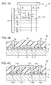
- FIG. 5 is a cross-sectional view schematically showing a protective circuit element provided in a thin film semiconductor device according to a second embodiment of the invention.
- FIG. 5 corresponds to FIG. 2B illustrating the first embodiment.
- the planar structure of a protective circuit element 281 according to the second embodiment is almost the same as that of the protective circuit element 181 shown in FIG. 2A.
- the protective circuit element 281 shown in FIG. 5 includes a PIN diode 281a and a floating electrode 118g serving as main elements.
- a low concentration impurity region 218n serving as a region whose impurity concentration is lower than that of an N layer 118n.
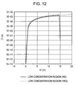
- FIG. 12 is a graph showing the results of comparing voltage-current characteristics between the protective circuit element according to the present embodiment and the protective circuit element according to the first embodiment.
- a horizontal axis indicates the application voltage
- a vertical axis indicates the current.
- a solid line indicates : characteristics of the element according to the first embodiment, which does not have the low concentration region between the I layer and the N layer
- a broken line indicates characteristics of a protection element according to the second embodiment, which has the low concentration region between the I layer and the N layer. From FIG. 12, it can be clearly seen that the broken line exceeds 15 V, and the withstand voltage of the protective circuit element according to the present embodiment increases.
- the withstand voltage of the protective circuit element can increase and the withstand voltage of the protective circuit can also increase, which the reliability is further improved.
- the LDD Lightly Doped Drain
- the TFT can be easily formed in the same process as the TFT of the internal circuits, in the same manner as the protective circuit element 181 according to the first embodiment.
- FIG. 6 is a cross-sectional view schematically showing a protective circuit element provided in a thin film semiconductor device according to a third embodiment of the invention.
- FIG. 6 corresponds to FIG. 2B illustrating the first embodiment.
- the planar structure of a protective circuit element 381 according to the present embodiment is the same as that of the protective circuit element 181 shown in FIG. 2A.
- the protective circuit element 381 shown in FIG. 6 includes a PIN diode 381a and a floating electrode 118g as main elements.
- the PIN diode 381a is the same as the PIN diode 281a shown in FIG. 5 in that between an N layer 118n and an I layer 118i disposed at a location where a semiconductor film 118s of the PIN diode 381a and the floating electrode 118g overlap each other in plan view, formed is a low concentration impurity region 318n serving as a region whose impurity concentration is lower than that of an N layer 118n.
- the low concentration impurity region 318n is formed at a location where it overlaps the floating electrode 118g in plan view.
- the structure of the protective circuit element 381 is similar to that of a TFT having a so-called GOLDD (Gate Overlapped Lightly Dopped Drain) structure.
- GOLDD Gate Overlapped Lightly Dopped Drain
- the protective circuit element can be easily formed in the same process as the internal circuits, and a PIN diode having the high withstand voltage can also be formed in the same manner as the second embodiment.
- the upper side metal film (a side opposite to a semiconductor film) of the corresponding gate electrode is formed to have an area narrower than that of the lower metal film thereof.
- an impurity is introduced into the semiconductor film by using the gate electrode as a mask.
- a low concentration impurity region can be formed in the semiconductor film in a self-aligned manner so as to correspond to the region where the lower metal film is larger than the upper metal film.
- the floating electrode 118g is formed to have the two-layer structure in the same manner as the gate electrode of the TFT having the GOLDD structure, and an impurity is implanted into the N layer 118n.
- the low concentration impurity region 318n can be thus formed within the planar region of the floating electrode 118g.
- FIG. 7 is a cross-sectional view schematically showing a protective circuit element provided in a thin film semiconductor device according to a fourth embodiment of the invention.
- FIG. 7 corresponds to FIG. 2B illustrating the first embodiment.
- the planar structure of a protective circuit element 481 according to the present embodiment is the same as that of the protective circuit element 181 shown in FIG. 2A.
- the protective circuit element 481 shown in FIG. 7 includes a PIN diode 481a and a floating electrode 118g serving as main elements.
- the present embodiment is the same as the above-mentioned first to third embodiments in that the I layer 118i is disposed at a location where the semiconductor film 118s of the PIN diode 481a and the floating electrode 118g overlap each other in plan view, but is different from the first to third embodiments in that the N layer 118n extends to a region where the floating electrode 118g and the semiconductor film 118s overlap each other in plan view. Even though the PIN diode 481a having this extending portion 418n of the N layer is used, the same effects as those of the above-mentioned embodiments can be obtained.
- the low concentration impurity regions 218n and 318n are provided between the P layer 118p and the I layer 118i and between the N layer 118n and I layer 118i and the floating electrode 118g extends up to over the P layer 118p or the N layer 118n of the PIN diode shown in the second and third embodiments, a protective circuit element having the same high withstand voltage and a protection function against the surge voltage of a backward direction can be provided.
- the gate electrode and the impurity-introduced region e.g., a drain region
- the TFT having the structure is formed as the internal circuit, it is effective to use a protective circuit element having the PIN diode 481a according to the present embodiment in terms of the standardization of the manufacturing process.
- FIG. 8 is a perspective view illustrating an example of a cellular phone.
- a reference numeral 1300 indicates a cellular phone body
- a reference numeral 1301 indicates a display unit using the liquid crystal display device.
- a reference numeral 1302 indicates an operating portion
- reference numerals 1303 and 1304 indicate an earpiece and a mouthpiece, respectively.
- the electronic apparatus shown in FIG. 8 has the display unit using the liquid crystal display device according to the above-described embodiments. It is thus possible to realize an electronic apparatus having the liquid crystal display unit with high reliability and a long life span.
- the invention has been described with reference to the particular illustrative embodiments, it is not limited to the embodiments but only by the appended claims. It is to be appreciated that those skilled in the art can change or modify the embodiments without departing from the scope and spirit of the invention.
- the invention can be applied to electro-optical devices using an active matrix substrate, and can also be applied to light-emitting devices of a current driving type, such as organic EL displays, as well as liquid crystal display devices.
- a current driving type such as organic EL displays
- the arrangement of peripheral circuits such as a data line driving circuit and a scanning line driving circuit, is not limited to the above-mentioned embodiments, but can be arbitrarily modified.
Applications Claiming Priority (2)
| Application Number | Priority Date | Filing Date | Title |
|---|---|---|---|
| JP2004215333 | 2004-07-23 | ||
| JP2005114230A JP2006060191A (ja) | 2004-07-23 | 2005-04-12 | 薄膜半導体装置及びその製造方法、電気光学装置、電子機器 |
Publications (2)
| Publication Number | Publication Date |
|---|---|
| EP1619725A2 true EP1619725A2 (fr) | 2006-01-25 |
| EP1619725A3 EP1619725A3 (fr) | 2009-04-08 |
Family
ID=35311881
Family Applications (1)
| Application Number | Title | Priority Date | Filing Date |
|---|---|---|---|
| EP05013531A Withdrawn EP1619725A3 (fr) | 2004-07-23 | 2005-06-23 | Dispositif semiconducteur à couche mince et son procédé de fabrication, dispositif électro-optique et appareil électronique |
Country Status (5)
| Country | Link |
|---|---|
| US (1) | US20060017139A1 (fr) |
| EP (1) | EP1619725A3 (fr) |
| JP (1) | JP2006060191A (fr) |
| KR (1) | KR100668272B1 (fr) |
| TW (1) | TWI283484B (fr) |
Cited By (7)
| Publication number | Priority date | Publication date | Assignee | Title |
|---|---|---|---|---|
| EP2012361A3 (fr) * | 2007-07-04 | 2010-08-18 | Samsung Mobile Display Co., Ltd. | Élément électroluminescent organique et son procédé de fabrication |
| US8174047B2 (en) | 2008-07-10 | 2012-05-08 | Semiconductor Energy Laboratory Co., Ltd. | Semiconductor device |
| US8368145B2 (en) | 2008-06-25 | 2013-02-05 | Semiconductor Energy Laboratory Co., Ltd. | Semiconductor device and electronic device |
| US8749930B2 (en) | 2009-02-09 | 2014-06-10 | Semiconductor Energy Laboratory Co., Ltd. | Protection circuit, semiconductor device, photoelectric conversion device, and electronic device |
| US9842863B2 (en) | 2012-11-28 | 2017-12-12 | Semiconductor Energy Laboratory Co., Ltd. | Display device and electronic device |
| WO2018116263A1 (fr) * | 2016-12-24 | 2018-06-28 | Indian Institute Of Science | Circuit de protection contre les décharges électrostatiques de faible puissance |
| EP3242159A4 (fr) * | 2015-01-04 | 2018-09-05 | Boe Technology Group Co. Ltd. | Substrat matriciel et son procédé de fabrication, panneau d'affichage et dispositif d'affichage |
Families Citing this family (19)
| Publication number | Priority date | Publication date | Assignee | Title |
|---|---|---|---|---|
| US20070069237A1 (en) * | 2005-09-29 | 2007-03-29 | Toppoly Optoelectronics Corp. | Systems for providing electrostatic discharge protection |
| DE102006023429B4 (de) * | 2006-05-18 | 2011-03-10 | Infineon Technologies Ag | ESD-Schutz-Element zur Verwendung in einem elektrischen Schaltkreis |
| US20070268637A1 (en) * | 2006-05-18 | 2007-11-22 | Prime View International Co., Ltd. | Active matrix device |
| US7781768B2 (en) * | 2006-06-29 | 2010-08-24 | Semiconductor Energy Laboratory Co., Ltd. | Display device, method for manufacturing the same, and electronic device having the same |
| WO2008001517A1 (fr) | 2006-06-30 | 2008-01-03 | Sharp Kabushiki Kaisha | Substrat de transistor à couches minces, panneau d'affichage et dispositif d'affichage munis d'un tel substrat de transistor à couches minces, et procédé de fabrication d'un substrat de transistor à couches minces |
| TW200947822A (en) * | 2008-05-09 | 2009-11-16 | Tpo Displays Corp | Electrostatic discharge (ESD) protection circuit and electronic system utilizing the same |
| US8363365B2 (en) * | 2008-06-17 | 2013-01-29 | Semiconductor Energy Laboratory Co., Ltd. | Semiconductor device |
| US8384180B2 (en) * | 2009-01-22 | 2013-02-26 | Palo Alto Research Center Incorporated | Gated co-planar poly-silicon thin film diode |
| JP5455753B2 (ja) * | 2009-04-06 | 2014-03-26 | 株式会社半導体エネルギー研究所 | Icカード |
| JP5728171B2 (ja) | 2009-06-29 | 2015-06-03 | 株式会社半導体エネルギー研究所 | 半導体装置 |
| WO2011043183A1 (fr) * | 2009-10-07 | 2011-04-14 | シャープ株式会社 | Dispositif à semi-conducteur, procédé de fabrication du dispositif à semi-conducteur et dispositif d'affichage équipé du dispositif à semi-conducteur |
| WO2011052437A1 (fr) * | 2009-10-30 | 2011-05-05 | Semiconductor Energy Laboratory Co., Ltd. | Élément non linéaire, dispositif d'affichage comprenant un élément non linéaire, et dispositif électronique comprenant un dispositif d'affichage |
| KR101113421B1 (ko) * | 2009-11-23 | 2012-03-13 | 삼성모바일디스플레이주식회사 | 액정 표시 장치 |
| US8698137B2 (en) | 2011-09-14 | 2014-04-15 | Semiconductor Energy Laboratory Co., Ltd. | Semiconductor device |
| TWI820614B (zh) * | 2012-11-28 | 2023-11-01 | 日商半導體能源研究所股份有限公司 | 顯示裝置 |
| KR20150026066A (ko) * | 2013-08-30 | 2015-03-11 | 삼성전자주식회사 | 터널링 전계 효과 트랜지스터 |
| JP6364891B2 (ja) * | 2014-04-01 | 2018-08-01 | セイコーエプソン株式会社 | 電気光学装置、電子機器および半導体装置 |
| JP2016015404A (ja) * | 2014-07-02 | 2016-01-28 | 株式会社ジャパンディスプレイ | 液晶表示装置 |
| US9397084B1 (en) * | 2015-03-02 | 2016-07-19 | United Microelectronics Corp. | Structure of ESD protection circuits on BEOL layer |
Citations (5)
| Publication number | Priority date | Publication date | Assignee | Title |
|---|---|---|---|---|
| WO1996022613A1 (fr) * | 1995-01-20 | 1996-07-25 | Peregrine Semiconductor Corporation | Procede et structure permettant de fournir une protection contre les decharges electriques pour des circuits integres silicium sur isolant |
| US5585949A (en) * | 1991-03-25 | 1996-12-17 | Semiconductor Energy Laboratory Co., Ltd. | Electro-optical device |
| US5616944A (en) * | 1990-05-21 | 1997-04-01 | Canon Kabushiki Kaisha | Diode and semiconductor device having a controlled intrinsic or low impurity concentration region between opposite conductivity type semiconductor regions |
| US6657240B1 (en) * | 2002-01-28 | 2003-12-02 | Taiwan Semiconductoring Manufacturing Company | Gate-controlled, negative resistance diode device using band-to-band tunneling |
| WO2004012267A2 (fr) * | 2002-07-30 | 2004-02-05 | Honeywell International Inc. | Protection contre les surtensions au moyen de diodes pin |
Family Cites Families (6)
| Publication number | Priority date | Publication date | Assignee | Title |
|---|---|---|---|---|
| JP3717227B2 (ja) * | 1996-03-29 | 2005-11-16 | 株式会社ルネサステクノロジ | 入力/出力保護回路 |
| JP4813743B2 (ja) * | 2002-07-24 | 2011-11-09 | 株式会社 日立ディスプレイズ | 画像表示装置の製造方法 |
| TWI357616B (en) * | 2002-09-20 | 2012-02-01 | Semiconductor Energy Lab | Display device and manufacturing method thereof |
| TW587345B (en) * | 2003-02-21 | 2004-05-11 | Toppoly Optoelectronics Corp | Method and structure of diode |
| JP2005043672A (ja) * | 2003-07-22 | 2005-02-17 | Toshiba Matsushita Display Technology Co Ltd | アレイ基板およびその製造方法 |
| US7314785B2 (en) * | 2003-10-24 | 2008-01-01 | Semiconductor Energy Laboratory Co., Ltd. | Display device and manufacturing method thereof |
-
2005
- 2005-04-12 JP JP2005114230A patent/JP2006060191A/ja active Pending
- 2005-06-08 US US11/147,250 patent/US20060017139A1/en not_active Abandoned
- 2005-06-23 EP EP05013531A patent/EP1619725A3/fr not_active Withdrawn
- 2005-07-19 KR KR1020050065151A patent/KR100668272B1/ko active IP Right Grant
- 2005-07-21 TW TW094124765A patent/TWI283484B/zh not_active IP Right Cessation
Patent Citations (5)
| Publication number | Priority date | Publication date | Assignee | Title |
|---|---|---|---|---|
| US5616944A (en) * | 1990-05-21 | 1997-04-01 | Canon Kabushiki Kaisha | Diode and semiconductor device having a controlled intrinsic or low impurity concentration region between opposite conductivity type semiconductor regions |
| US5585949A (en) * | 1991-03-25 | 1996-12-17 | Semiconductor Energy Laboratory Co., Ltd. | Electro-optical device |
| WO1996022613A1 (fr) * | 1995-01-20 | 1996-07-25 | Peregrine Semiconductor Corporation | Procede et structure permettant de fournir une protection contre les decharges electriques pour des circuits integres silicium sur isolant |
| US6657240B1 (en) * | 2002-01-28 | 2003-12-02 | Taiwan Semiconductoring Manufacturing Company | Gate-controlled, negative resistance diode device using band-to-band tunneling |
| WO2004012267A2 (fr) * | 2002-07-30 | 2004-02-05 | Honeywell International Inc. | Protection contre les surtensions au moyen de diodes pin |
Cited By (10)
| Publication number | Priority date | Publication date | Assignee | Title |
|---|---|---|---|---|
| EP2012361A3 (fr) * | 2007-07-04 | 2010-08-18 | Samsung Mobile Display Co., Ltd. | Élément électroluminescent organique et son procédé de fabrication |
| US8592881B2 (en) | 2007-07-04 | 2013-11-26 | Samsung Display Co., Ltd. | Organic light emitting element and method of manufacturing the same |
| US9368558B2 (en) | 2007-07-04 | 2016-06-14 | Samsung Display Co., Ltd. | Organic light emitting element and method of manufacturing the same |
| US8368145B2 (en) | 2008-06-25 | 2013-02-05 | Semiconductor Energy Laboratory Co., Ltd. | Semiconductor device and electronic device |
| US8174047B2 (en) | 2008-07-10 | 2012-05-08 | Semiconductor Energy Laboratory Co., Ltd. | Semiconductor device |
| US8860081B2 (en) | 2008-07-10 | 2014-10-14 | Semiconductor Energy Laboratory Co., Ltd. | Semiconductor device |
| US8749930B2 (en) | 2009-02-09 | 2014-06-10 | Semiconductor Energy Laboratory Co., Ltd. | Protection circuit, semiconductor device, photoelectric conversion device, and electronic device |
| US9842863B2 (en) | 2012-11-28 | 2017-12-12 | Semiconductor Energy Laboratory Co., Ltd. | Display device and electronic device |
| EP3242159A4 (fr) * | 2015-01-04 | 2018-09-05 | Boe Technology Group Co. Ltd. | Substrat matriciel et son procédé de fabrication, panneau d'affichage et dispositif d'affichage |
| WO2018116263A1 (fr) * | 2016-12-24 | 2018-06-28 | Indian Institute Of Science | Circuit de protection contre les décharges électrostatiques de faible puissance |
Also Published As
| Publication number | Publication date |
|---|---|
| EP1619725A3 (fr) | 2009-04-08 |
| TW200618304A (en) | 2006-06-01 |
| KR20060053881A (ko) | 2006-05-22 |
| US20060017139A1 (en) | 2006-01-26 |
| TWI283484B (en) | 2007-07-01 |
| JP2006060191A (ja) | 2006-03-02 |
| KR100668272B1 (ko) | 2007-01-12 |
Similar Documents
| Publication | Publication Date | Title |
|---|---|---|
| EP1619725A2 (fr) | Dispositif semiconducteur à couche mince et son procédé de fabrication, dispositif électro-optique et appareil électronique | |
| CN110366779B (zh) | 具有硅顶栅薄膜晶体管和半导体氧化物顶栅薄膜晶体管的显示器 | |
| US10256226B2 (en) | Display device including electrostatic discharge circuit | |
| US6671146B1 (en) | Electrostatic protection circuit and semiconductor integrated circuit using the same | |
| KR100235133B1 (ko) | 반도체장치 | |
| KR100249716B1 (ko) | 반도체 장치 | |
| KR101923763B1 (ko) | 레벨 쉬프트 회로 보호용 정전기 방전 보호 회로 및 소자 | |
| US20060237815A1 (en) | High voltage integrated circuit device including high-voltage resistant diode | |
| US6838700B2 (en) | Active matrix substrate | |
| US20070001949A1 (en) | Protective circuit for a thin film transistor and a liquid crystal display device | |
| US20210399142A1 (en) | Thin Film Transistor Array Substrate and Display Device | |
| KR100387189B1 (ko) | 절연체상반도체장치및그보호회로 | |
| US5739571A (en) | Semiconductor device having protection device for preventing the electrostatic breakdown of output buffer MOSFETs | |
| US20060118787A1 (en) | Electronic device with electrostatic discharge protection | |
| CN100454553C (zh) | 薄膜半导体装置及其制造方法、电光学装置、电子机器 | |
| US8072033B2 (en) | Semiconductor device having elongated electrostatic protection element along long side of semiconductor chip | |
| US20060001098A1 (en) | Electrostatic discharge protection device | |
| US5729044A (en) | Protection diode for a vertical semiconductor component | |
| KR100234860B1 (ko) | Cmos 반도체 장치 | |
| US7723794B2 (en) | Load driving device | |
| CN111564460B (zh) | 有源矩阵基板及具备该有源矩阵基板的光电转换拍摄面板 | |
| KR20030051388A (ko) | 폴리실리콘 유계 스냅백 장치 | |
| JP3141511B2 (ja) | 信号入力回路およびアクティブマトリクスパネル | |
| US11735581B2 (en) | Electrostatic protection structure comprising electrostatic protection units containing TFT's, TFT substrate, and display panel | |
| JP3442331B2 (ja) | 半導体装置 |
Legal Events
| Date | Code | Title | Description |
|---|---|---|---|
| PUAI | Public reference made under article 153(3) epc to a published international application that has entered the european phase |
Free format text: ORIGINAL CODE: 0009012 |
|
| AK | Designated contracting states |
Kind code of ref document: A2 Designated state(s): AT BE BG CH CY CZ DE DK EE ES FI FR GB GR HU IE IS IT LI LT LU MC NL PL PT RO SE SI SK TR |
|
| AX | Request for extension of the european patent |
Extension state: AL BA HR LV MK YU |
|
| PUAL | Search report despatched |
Free format text: ORIGINAL CODE: 0009013 |
|
| AK | Designated contracting states |
Kind code of ref document: A3 Designated state(s): AT BE BG CH CY CZ DE DK EE ES FI FR GB GR HU IE IS IT LI LT LU MC NL PL PT RO SE SI SK TR |
|
| AX | Request for extension of the european patent |
Extension state: AL BA HR LV MK YU |
|
| STAA | Information on the status of an ep patent application or granted ep patent |
Free format text: STATUS: THE APPLICATION HAS BEEN WITHDRAWN |
|
| 18W | Application withdrawn |
Effective date: 20090616 |