EP1617455B1 - Farbbildröhre - Google Patents
Farbbildröhre Download PDFInfo
- Publication number
- EP1617455B1 EP1617455B1 EP05253331A EP05253331A EP1617455B1 EP 1617455 B1 EP1617455 B1 EP 1617455B1 EP 05253331 A EP05253331 A EP 05253331A EP 05253331 A EP05253331 A EP 05253331A EP 1617455 B1 EP1617455 B1 EP 1617455B1
- Authority
- EP
- European Patent Office
- Prior art keywords
- curve
- sagging amount
- shadow mask
- panel
- point
- Prior art date
- Legal status (The legal status is an assumption and is not a legal conclusion. Google has not performed a legal analysis and makes no representation as to the accuracy of the status listed.)
- Ceased
Links
- 238000007665 sagging Methods 0.000 claims description 157
- OAICVXFJPJFONN-UHFFFAOYSA-N Phosphorus Chemical compound [P] OAICVXFJPJFONN-UHFFFAOYSA-N 0.000 claims description 38
- 238000010894 electron beam technology Methods 0.000 claims description 37
- XEEYBQQBJWHFJM-UHFFFAOYSA-N Iron Chemical compound [Fe] XEEYBQQBJWHFJM-UHFFFAOYSA-N 0.000 claims description 25
- 239000000463 material Substances 0.000 claims description 17
- 229910052742 iron Inorganic materials 0.000 claims description 12
- 239000003086 colorant Substances 0.000 claims description 4
- 238000002834 transmittance Methods 0.000 claims description 2
- 230000000694 effects Effects 0.000 description 13
- 230000015556 catabolic process Effects 0.000 description 9
- 238000006731 degradation reaction Methods 0.000 description 9
- 238000000465 moulding Methods 0.000 description 9
- 229910045601 alloy Inorganic materials 0.000 description 8
- 239000000956 alloy Substances 0.000 description 8
- PXHVJJICTQNCMI-UHFFFAOYSA-N Nickel Chemical compound [Ni] PXHVJJICTQNCMI-UHFFFAOYSA-N 0.000 description 6
- 229910001374 Invar Inorganic materials 0.000 description 5
- 230000007423 decrease Effects 0.000 description 5
- 238000004519 manufacturing process Methods 0.000 description 4
- 229910001030 Iron–nickel alloy Inorganic materials 0.000 description 3
- 230000003247 decreasing effect Effects 0.000 description 3
- 238000006073 displacement reaction Methods 0.000 description 3
- 238000000034 method Methods 0.000 description 3
- 229910000655 Killed steel Inorganic materials 0.000 description 2
- 229910052782 aluminium Inorganic materials 0.000 description 2
- XAGFODPZIPBFFR-UHFFFAOYSA-N aluminium Chemical compound [Al] XAGFODPZIPBFFR-UHFFFAOYSA-N 0.000 description 2
- 238000000137 annealing Methods 0.000 description 2
- 238000005336 cracking Methods 0.000 description 2
- 229910052759 nickel Inorganic materials 0.000 description 2
- 230000035882 stress Effects 0.000 description 2
- 229910000416 bismuth oxide Inorganic materials 0.000 description 1
- TYIXMATWDRGMPF-UHFFFAOYSA-N dibismuth;oxygen(2-) Chemical compound [O-2].[O-2].[O-2].[Bi+3].[Bi+3] TYIXMATWDRGMPF-UHFFFAOYSA-N 0.000 description 1
- 238000004880 explosion Methods 0.000 description 1
- 238000010438 heat treatment Methods 0.000 description 1
- 230000001678 irradiating effect Effects 0.000 description 1
- 230000002093 peripheral effect Effects 0.000 description 1
- 230000008646 thermal stress Effects 0.000 description 1
Images


Classifications
-
- H—ELECTRICITY
- H01—ELECTRIC ELEMENTS
- H01J—ELECTRIC DISCHARGE TUBES OR DISCHARGE LAMPS
- H01J29/00—Details of cathode-ray tubes or of electron-beam tubes of the types covered by group H01J31/00
- H01J29/02—Electrodes; Screens; Mounting, supporting, spacing or insulating thereof
- H01J29/06—Screens for shielding; Masks interposed in the electron stream
- H01J29/07—Shadow masks for colour television tubes
-
- H—ELECTRICITY
- H01—ELECTRIC ELEMENTS
- H01J—ELECTRIC DISCHARGE TUBES OR DISCHARGE LAMPS
- H01J29/00—Details of cathode-ray tubes or of electron-beam tubes of the types covered by group H01J31/00
- H01J29/86—Vessels; Containers; Vacuum locks
- H01J29/861—Vessels or containers characterised by the form or the structure thereof
-
- H—ELECTRICITY
- H01—ELECTRIC ELEMENTS
- H01J—ELECTRIC DISCHARGE TUBES OR DISCHARGE LAMPS
- H01J2229/00—Details of cathode ray tubes or electron beam tubes
- H01J2229/07—Shadow masks
- H01J2229/0727—Aperture plate
- H01J2229/0788—Parameterised dimensions of aperture plate, e.g. relationships, polynomial expressions
-
- H—ELECTRICITY
- H01—ELECTRIC ELEMENTS
- H01J—ELECTRIC DISCHARGE TUBES OR DISCHARGE LAMPS
- H01J2229/00—Details of cathode ray tubes or electron beam tubes
- H01J2229/07—Shadow masks
- H01J2229/0794—Geometrical arrangements, e.g. curvature
-
- H—ELECTRICITY
- H01—ELECTRIC ELEMENTS
- H01J—ELECTRIC DISCHARGE TUBES OR DISCHARGE LAMPS
- H01J2229/00—Details of cathode ray tubes or electron beam tubes
- H01J2229/86—Vessels and containers
- H01J2229/8613—Faceplates
- H01J2229/8616—Faceplates characterised by shape
- H01J2229/862—Parameterised shape, e.g. expression, relationship or equation
Definitions
- the present invention relates to a color picture tube provided with a shadow mask.
- a color picture tube includes an envelope composed of a substantially rectangular panel 3 in which a skirt portion 2 is provided on the periphery of a useful surface 1 formed of a curved surface, and a funnel 4 in a funnel shape connected to the skirt portion 2.
- a substantially rectangular shadow mask 7 having a curved surface, in which a number of electron beam passage apertures 6 are formed, is placed so as to be opposed to a phosphor screen 5 composed of three-color phosphor layers formed on an inner surface of the useful surface 1 of the panel 3.
- the shadow mask 7 is held by a substantially rectangular mask frame 8.
- a shadow mask structure 9 composed of the shadow mask 7 and the mask frame 8 is supported detachably with respect to the panel 3 with one end of a substantially V-shaped elastic support 15 attached to each corner portion or respectively on a short side and a long side of the mask frame 8, and the other end of the elastic support 15 engaged with a stud pin 16 fixed on an inner wall of the skirt portion 2 of the panel 3.
- An electron gun 12 emitting three electron beams 11 is housed in a neck 10 of the funnel 4.
- the three electron beams 11 emitted by the electron gun 12 are deflected by a magnetic field generated by a deflection apparatus 13 mounted on an outer side of the funnel 4, and allowed to scan the phosphor screen 5 in horizontal and vertical directions via the shadow mask 7, thereby displaying a color image.
- the three electron beams 11 passing through the electron beam passage apertures 6 formed in the shadow mask 7 should land correctly on the three-color phosphor layers of the phosphor screen 5 respectively.
- the relative amount of the electron beams 11 that pass through the electron beam passage apertures 6 of the shadow mask 7 to reach the phosphor screen 5 is 1/3 or less of the total amount of the electron beams emitted by the electron gun 12, and the other electron beams strike the shadow mask 7 to be converted into thermal energy.
- a so-called doming phenomenon occurs. That is, the shadow mask 7 is heated to expand thermally, and consequently, is deformed so as to swell on the phosphor screen 5 side.
- the interval q between the phosphor screen 5 and the shadow mask 7 exceeds an allowable range due to the doming, the landing position of the electron beams 11 with respect to the phosphor screen 5 shifts to degrade color purity.
- the magnitude of the landing positional shift of the electron beams 11 caused by the thermal expansion of the shadow mask 7 varies largely depending upon the brightness of an image pattern and the duration time of the pattern. Particularly, in the case of locally displaying an image pattern with high brightness, local doming occurs, and a local landing positional shift occurs within a short period of time. In the local doming, the amount of the landing positional shift is large.
- a center of the shadow mask 7 i.e., a point where a tube axis (Z-axis) crosses
- P0 an axis orthogonal to the tube axis and parallel to a long side
- X-axis an axis orthogonal to the tube axis and the major axis and parallel to a short side
- Y-axis an axis orthogonal to the tube axis and the major axis and parallel to a short side
- W an interval between the center P0 and an useful area end of the shadow mask 7 along the major axis
- the above-mentioned local doming occurs most remarkably in the case where a pattern with high brightness is displayed in an area on the phosphor screen 5 corresponding to an oval area 30 including a point P1 on the major axis away from the center P0 by (2/3) x W, and the landing positional shift of the electron beams in the area on the phosphor screen 5 corresponding to the area 30 is largest.
- an alloy mainly containing iron and nickel, having a low coefficient of thermal expansion is used generally as a material for the shadow mask 7.
- an iron-nickel alloy such as 36 Ni Invar alloy (see Table 3 described later) is used.
- Such an alloy entails high cost, while having a coefficient of thermal expansion of 1 to 2 x 10 -6 at 0°C to 100°C, and being effective for suppressing doming.
- the iron-nickel alloy has large elasticity after annealing, so that it is difficult to form a curved surface from such an alloy by molding and to obtain a desired curved surface. Even if the iron-nickel alloy is annealed, for example, at a high temperature of 900°C, the yield point strength is about 28 x 10 7 N/m 2 . Thus, it is necessary to treat the alloy at a considerably high temperature in order to set the yield point strength to be 20 x 10 7 N/m 2 or less at which molding generally is considered to be easy. Particularly, in a color picture tube with a flat panel outer surface, the curvature of the shadow mask 7 is small, so that molding is further difficult.
- the yield point strength can be set to be 20 x 10 7 N/m 2 or less by annealing at about 800°C, so that molding is very easy.
- the mold temperature it is not necessary to keep the mold temperature to be high in the course of molding, which is required in an Invar alloy, and the productivity also is satisfactory.
- the coefficient of thermal expansion of the material mainly containing iron with high purity is high (i.e., about 12 x 10 -6 at 0°C to 100°C), which is disadvantageous for doming.
- the coefficient of thermal expansion of the material mainly containing iron with high purity is high (i.e., about 12 x 10 -6 at 0°C to 100°C), which is disadvantageous for doming.
- a serious problem such as the significant degradation in color purity.
- JP 10(1998)-199436 A discloses a shadow mask in the shape of a substantially cylindrical surface, in which the radius of curvature in a major axis direction is almost infinite, and the radius of curvature in a minor axis direction is almost constant irrespective of the position in the major axis direction. Even such a shadow mask has an effect of suppressing doming to some degree. However, in the case of using an inexpensive iron material, a sufficient effect cannot be obtained.
- JP 2004-31305 A discloses a cathode-ray tube using an inexpensive iron material for a shadow mask by defining the radius of curvature of a panel inner surface.
- a sufficient effect of suppressing doming cannot be obtained, either, in the same way as in JP 10(1998)-199436 A .
- the weight of a panel increases, compared with the case of using an expensive Invar material.
- EP 1115139 describes a color picture tube.
- EP 1258904 describes a color cathode ray tube having a flat outer face.
- EP 1089313 describes a color cathode ray tube with a flat panel face.
- EP 1061548 describes a color cathode ray tube.
- EP 0692810 describes a color cathode ray tube.
- EP 0578251 describes a color cathode ray tube.
- a color picture tube can be provided having satisfactory visibility and less degradation in color purity caused by doming while having an inexpensive shadow mask.
- FIG. 1 is a cross-sectional view of a color picture tube.
- the color picture tube includes an envelope composed of a substantially rectangular panel 3 in which a skirt portion 2 is provided on the periphery of an useful surface 1 on which an image is displayed, and a funnel 4 in a funnel shape connected to the skirt portion 2.
- a substantially rectangular shadow mask 7 having a curved surface in which a number of electron beam passage apertures 6 are formed is placed so as to be opposed to a phosphor screen 5 made of three-color phosphor layers formed on an inner surface of the useful surface 1 of the panel 3.
- the shadow mask 7 is held by a substantially rectangular mask frame 8 having a substantially L-shaped cross-section.
- a shadow mask structure 9 composed of the shadow mask 7 and the mask frame 8 is supported detachably with respect to the panel 3 with one end of a substantially V-shaped elastic support 15 attached to each corner portion or respectively on a short side and a long side of the mask frame 8, and the other end of the elastic support 15 engaged with a stud pin 16 fixed on an inner wall of the skirt portion 2 of the panel 3.
- An electron gun 12 emitting three electron beams 11 is housed in a neck 10 of the funnel 4.
- the three electron beams 11 emitted by the electron gun 12 are deflected by a magnetic field generated by a deflection apparatus 13 mounted on an outer side of the funnel 4, and allowed to scan the phosphor screen 5 in horizontal and vertical directions via the shadow mask 7, thereby displaying a color image.
- the three electron beams 11 passing through the electron beam passage apertures 6 formed in the shadow mask 7 should land correctly on the three-color phosphor layers of the phosphor screen 5 respectively. For this purpose, it is necessary to maintain the correct position between the panel 3 and the shadow mask 7.
- the outer surface of the useful surface 1 of the panel 3 is being substantially flattened with a radius of curvature of 10,000 mm or more, and along with this, the shadow mask 7 also should be flattened.
- the present invention can solve the above-mentioned problems.
- One example thereof will be described below.
- FIG. 2 shows the sagging amount of a surface of the shadow mask 7 used for a color picture tube with a diagonal useful size of 51 cm, an aspect ratio of 4 : 3, and a radius of curvature of an outer surface of the useful surface 1 of the panel 3 of 20,000 mm.
- the sagging amount refers to a displacement amount (the side of the electron gun 12 is assumed to be positive) in a tube axis (Z-axis) direction of the surface (surface opposed to the phosphor screen 5) of the shadow mask 7.
- a center (i.e., a point where the tube axis (Z-axis) crosses) of the substantially rectangular shadow mask 7 is P0
- an axis orthogonal to the tube axis and parallel to a long side is a major axis (X-axis)
- an axis orthogonal to the tube axis and the major axis and parallel to a short side is a minor axis (Y-axis).
- a "major axis” represents a sagging amount change curve along a curve C1 on the surface of the shadow mask 7, which a plane passing through the center P0 and parallel to the tube axis and the major axis crosses in FIG. 3.
- a position (reference point) at which the "coordinate” of a horizontal axis is 0 in FIG 2, corresponds to the center P0.
- the "useful area" of the shadow mask 7 refers to an area on the shadow mask 7 in which a number of electron beam passage apertures are formed.
- a “minor axis” represents a sagging amount change curve along a curve C3 on the surface of the shadow mask 7, which a plane passing through the center P0 and parallel to the tube axis and the minor axis crosses in FIG. 3.
- a position (reference point), at which the "coordinate" of the horizontal axis is 0 in FIG. 2 corresponds to the center P0.
- a "short side” represents a sagging amount change curve along a curve C4 on the surface of the shadow mask 7, which a plane passing through the major axis end PL and parallel to the tube axis and the minor axis crosses in FIG. 3.
- a position (reference point), at which the "coordinate" of the horizontal axis is 0 in FIG. 2 corresponds to the major axis end PL.
- the vertical axis in FIG. 2 shows a sagging amount with respect to the center P0.
- the shadow mask 7 has a spline curved surface in which the sagging amount change curves shown in FIG. 2 along the curves C 1, C2 satisfy the following conditions.
- a sagging amount at the useful area end with respect to the reference point is Ze
- a first sagging amount curve representing a first sagging amount Z1 at a point at a distance d from the reference point in a direction vertical to the tube axis represented by the following Formula 1
- a second sagging amount curve representing a second sagging amount Z2 at a point at the distance d from the reference point in the direction vertical to the tube axis represented by the following Formula 2
- Z ⁇ 1 ⁇ Ze • 1 - rf ⁇ 1 / L 2 ⁇ d 2 + ( Ze • rf ⁇ 1 ) / L 4 • d 4
- Z ⁇ 2 ⁇ Ze • 1 - rf ⁇ 2 / L 2 ⁇ d 2 + ( Ze • rf ⁇ 2 ) / L 4 • d 4
- the sagging amount change curve shown in FIG. 2 along the curve C1 satisfies the following Condition 1.
- the sagging amount change curve shown in FIG. 2 along the curve C2 satisfies the following Condition 2.
- the sagging amount change curve shown in FIG. 2 along the curve C3 satisfies the following Condition 3.
- the sagging amount change curve shown in FIG. 2 along the curve C4 satisfies the following Condition 4.
- FIG. 4 shows a relationship between the sagging amount change curve along the curve C1 and the doming.
- a "major axis midpoint” represents a doming amount at a midpoint between the center P0 and the major axis end PL
- a “diagonal midpoint” represents a doming amount at a midpoint between the center P0 and the diagonal end PD
- an "average” represents an average value of the doming amounts at both positions. At these positions, the doming amount is likely to become maximum in the shadow mask.
- FIG. 5 shows a relationship between the sagging amount change curve along the curve C2 and the doming.
- a "major axis midpoint” represents a doming amount at a midpoint between the center P0 and the major axis end PL
- a “diagonal midpoint” represents a doming amount at a midpoint between the center P0 and the diagonal end PD
- an "average” represents an average value of the doming amounts at both the positions. At these positions, the doming amount is likely to become maximum in the shadow mask.
- the sagging amount change curve along the curve C2 has a particularly large influence on doming.
- the following is found: when -0.4 ⁇ rf ⁇ 0 which satisfies the above-mentioned Condition 2, the balance between the doming amounts at both the positions is satisfactory, and the average value thereof is small, so that doming is suppressed effectively.
- Table 1 shows a maximum value of an electron beam movement amount on a screen caused by doming, when rf is varied in three ways in the sagging amount change curves obtained by the above-mentioned Formula 5 along the curves C1 and C2.
- L and Ze the same values as those in FIGS. 4 and 5 are used.
- Table 1 rf Maximum movement amount of electron beam caused by doming ( ⁇ m) Sagging amount change curve along curve C1 0.4 350 1.0 (present invention) 255 1.4 270 Sagging amount change curve along curve C2 -0.6 287 -0.2 (present invention) 255 0.4 320
- the sagging amount change curve along the curve C3 satisfies the above-mentioned Condition 3, since the following effect can be obtained.
- the problem of doming in an area slightly closer to the center P0 with respect to the point P1 can be solved.
- the curved surface holding strength (strength capable of holding a curved surface shape with respect to an external force) of the shadow mask 7 can be enhanced.
- the sagging amount change curve along the curve C4 satisfies the above-mentioned Condition 4
- the following effect is obtained.
- the problem of doming in an area slightly close to an outer side with respect to the point P1 can be solved.
- the curvature of the sagging amount change curve can be prevented from being reversed (i.e., the sagging amount change curve can be prevented from having an inflection point).
- a screen shape without any sense of incongruity is obtained.
- Table 2 shows a summary of electron beam movement amounts caused by doming at the point P1 in the case where a shadow mask has various kinds of surface shapes in color picture tubes with three types of screen diagonal useful sizes.
- a "single radius of curvature” represents the case where the shadow mask has a shape with a part of a spherical surface having a radius of curvature R cut away.
- a "cylindrical surface in a minor axis direction” represents the case where a shadow mask has a cylindrical surface shape in which the radius of curvature in the minor axis direction is constant irrespective of a position in the major axis direction as shown in the above-mentioned JP 10(1998)-199436 A .
- a “spline approximation” represents the case where the surface shape of a useful area of a shadow mask is composed of a spline approximated curved surface of x and y, where x represents a major axis direction and y represents a minor axis direction.
- a “biquadratic function approximation” represents the case where the surface shape of a useful area of a shadow mask is composed of a biquadratic function approximated curved surface of x and y, where x represents a major axis direction and y represents a minor axis direction.
- FIG. 2 shows sagging amount change curves along the curves C1 to C4 of a shadow mask of the "spline approximation" with a diagonal useful size of 51 cm
- FIG. 6 shows sagging amount change curves along the curves C1 to C4 of a shadow mask of the "spline approximation” with a diagonal useful size of 36 cm
- FIG. 7 shows sagging amount change curves along the curves C1 to C4 of a shadow mask of the "spline approximation” with a diagonal useful size of 60 cm.
- FIG. 6 shows a sagging amount of a shadow mask surface according to one example of the present invention having a spline approximated curved surface, used in a color picture tube with a diagonal useful size of 36 cm, an aspect ratio of 4 : 3, and a radius of curvature of an outer surface of the useful surface 1 of the panel 3 of 20,000 mm, in the same way as in FIG. 2. Furthermore, FIG.
- FIG. 7 shows a sagging amount of a shadow mask surface according to one example of the present invention having a spline approximated curved surface, used in a color picture tube with a diagonal useful size of 60 cm, an aspect ratio of 4 : 3, and a radius of curvature of an outer surface of the useful surface 1 of the panel 3 of 20,000 mm, in the same way as in FIG. 2.
- the difference in thickness between the center and the minor axis end of the panel increases, so that panel cracking caused by thermal distortion during a heating process in the course of production of a color picture tube increases.
- doming can be suppressed largely while the weight of a panel is kept equal to that in the case of the "single radius of curvature".
- the effect of suppressing doming can be obtained.
- the effect of suppressing doming is obtained with the same panel weight as that (9.5 kg) in the case of using an expensive Invar material.
- the doming occurring in the vicinity of the center of a screen of the shadow mask is almost negligible, since it is unlikely to influence the movement of the landing position of electron beams.
- the doming in the vicinity of the center of the screen, which is negligible is set to be relatively larger than that in the vicinity of the point P1 where the allowable range is narrowest. This can suppress the doming in the vicinity of the point P1.
- FIG. 8 shows a relationship between the sagging amount change curve ("major axis intermediate axis") along the curve C2 of the shadow mask shown in FIG. 2 and Condition 2 of the present invention.
- FIG. 9 shows a relationship between the sagging amount change curve along the curve C1 of the shadow mask having a single radius of curvature with a diagonal useful size of 51 cm, shown in Table 2 and Condition 1 of the present invention.
- a broken line represents the sagging amount change curve along the curve C1 of the shadow mask
- none of the portions of the sagging amount change curve along the curve C1 between the center P0 and the major axis end PL is present between the first sagging amount curve and the second sagging amount curve.
- Formula 3 defines the sagging amount Z MH at the major axis end.
- the sagging amount Z MH at the major axis end is increased too much, doming characteristics are degraded.
- the appropriate effect of suppressing doming can be obtained by satisfying Formula 3.
- Formula 4 defines a degree of sagging at the diagonal end.
- Z MD /D is larger, the curvature along the curve C2 most largely influencing doming becomes larger, so that the large effect of suppressing doming is obtained.
- Z MD /D is increased too much as in Embodiment 2 described later, the thickness of the screen useful area of the panel at the diagonal end also tends to increase.
- Z MD /D 0.071
- Z MD 16.8 mm
- Z MV 5.9 mm
- Z MH 10.9 mm.
- the outer surface of the useful surface 1 of the panel 3 is flattened sufficiently as described above, and satisfactory visibility is obtained.
- a material for the shadow mask 7 it is possible to use, for example, aluminum killed steel shown in Table 3 made of high-purity iron with a coefficient of thermal expansion of 12 x 10 -6 at 0°C to 100°C. Therefore, the moldability of the shadow mask 7 is satisfactory while entailing low cost. Then, doming can be suppressed as described above, so that a color picture tube with less degradation in color purity caused by doming can be provided.
- the surface of the useful area of the shadow mask 7 may be coated with bismuth oxide, whereby doming can be suppressed further.
- the interval q between the panel 3 and the shadow mask 7 is set appropriately over an entire range of a screen. Therefore, it is preferable that the inner surface of the panel 3 has a curvature close to that of the curved surface of the shadow mask 7.
- the shadow mask 7 is made of a material containing 95% or more of iron, and the surface thereof is set in a shape effective for suppressing doming, as described in Embodiment 1, it is preferable that the inner surface of the panel 3 satisfies the conditions similar to those in Embodiment 1. The reason for this is as follows.
- the phosphor screen 5 is formed by a light-exposure method using the shadow mask 7 as a mask. More specifically, as shown in FIG. 10, phosphor stripes of three colors (red, green, and blue) are obtained by irradiating the inner surface of the panel 3 with light beams from light sources 18R, 18G, and 18B of a light-exposure apparatus, approximated to paths of electron beams.
- PH P represents an arrangement pitch of phosphor stripes of three colors (red R, green G, and blue B), and is determined uniquely by the arrangement pitch of electron beam passage apertures of the shadow mask.
- s represents an interval between the center of the red phosphor stripe R and the center of the blue phosphor stripe B, and varies depending upon the interval q.
- s 2/3 PH P as shown in FIG. 11B, or s > 2/3 PH P as shown in FIG.
- the width of each black non-light-emitting layer (black stripe) 17 cannot be obtained sufficiently.
- the color purity during an operation of the color picture tube is likely to degrade.
- the pitch PH P is larger, the width of the black non-light-emitting layer 17 can be obtained more sufficiently.
- the pitch PH P is too large, the resolution degrades.
- the inner surface of the panel of the color picture tube according to the present embodiment is configured as follows.
- a distance from the reference point to the useful area end on the inner surface of the panel 3 in a direction vertical to the tube axis is L'
- a sagging amount at the useful area end with respect to the reference point is Ze'
- a first sagging amount curve representing a first sagging amount Z1' at a point at a distance d' from the reference point in a direction vertical to the tube axis represented by the following Formula 1'
- a second sagging amount curve representing a second sagging amount Z2' at a point at the distance d' from the reference point in the direction vertical to the tube axis represented by the following Formula 2'
- a center i.e., a point where the tube axis (Z-axis) crosses
- a center i.e., a point where the tube axis (Z-axis) crosses
- an axis orthogonal to the tube axis and parallel to a long side is a major axis (X-axis)
- an axis orthogonal to the tube axis and the major axis and parallel to a short side is a minor axis (Y-axis).
- a curve C1' is defined, which is obtained when a plane passing through the center P0' and parallel to the tube axis and the major axis crosses the inner surface of the panel 3.
- a curve C1' is defined, which is obtained when a plane passing through the point P1' and parallel to the tube axis and the minor axis crosses the inner surface of the panel 3.
- a curve C3' is defined, which is obtained when a plane passing through the center P0' and parallel to the tube axis and the minor axis crosses the inner surface of the panel 3.
- a curve C4' is defined, which is obtained when a plane passing through the major axis end PL' and parallel to the tube axis and the minor axis crosses the inner surface of the panel 3.
- the black non-light-emitting layers 17 with a uniform width can be formed.
- the sagging amount change curve along the curve C3' satisfies the following Condition 3'.
- the sagging amount change curve along the curve C4' satisfies the following Condition 4'.
- the "useful area" of the inner surface of the panel 3 refers to an area on the inner surface of the panel 3 where phosphor layers of three colors (red, green, and blue) are formed.
- FIG. 12 shows a relationship between the thickness ratio at the diagonal end PD' of the panel 3 with respect to the center P0', and the brightness ratio at the diagonal end PD' at that thickness ratio with respect to the center P0'.
- Tc a thickness of the panel 1 at the center P0'
- T D a thickness of the panel 1 at the diagonal end PD'
- T D /T C 2.1.
- the applicable field of the present invention is not particularly limited, and the present invention can be applied widely to a color picture tube for a TV, a computer display, etc.
Landscapes
- Electrodes For Cathode-Ray Tubes (AREA)
Claims (6)
- Farbbildröhre mit:einer Platte (3),einem Phosphor- bzw. Leuchtstoffbildschirm (5) in einer im wesentlichen rechteckigen Form, der auf einer inneren Oberfläche der Platte gebildet ist, undeiner Lochmaske (7) mit einem nutzbaren Bereich, in dem eine Anzahl von Elektronenstrahldurchgangsöffnungen (6) gebildet sind, die so plaziert ist, um gegenüber dem Leuchtstoffbildschirm (5) zu sein,
wobei ein Radius einer Krümmung einer äußeren Oberfläche der Platte (3) 10.000 mm oder mehr ist, unddie Lochmaske (7) aus einem Material gefertigt ist, das 95 % oder mehr Eisen enthält,die Farbbildröhre dadurch gekennzeichnet ist, dass die Lochmaske (7) so konfiguriert ist, dass:für eine Kurve C1, die auf der Oberfläche der Lochmaske (7) und in einer Ebene liegt, die durch die Mitte P0 des nutzbaren Bereichs der Lochmaske reicht und die parallel zu der Röhrenachse und einer Hauptachse der Lochmaske ist, dann zumindest 60 % der Durchbiege- bzw. Sinkbetragkurve entlang der Kurve C1 zwischen der Mitte P0 und dem Hauptachsenende PL, wo die Kurve C1 das Ende des nutzbaren Bereichs der Lochmaske schneidet, zwischen einer ersten Sinkbetragkurve, die repräsentiert ist durch:
und einer zweiten Sinkbetragkurve, die repräsentiert ist durch:
vorliegt, wobei:W der Abstand von der Mitte P0 zu dem Hauptachsenende PL, gemessen in einer Richtung parallel zu der Hauptachse ist, ZPL der Sinkbetrag in der Röhrenachsenrichtung bei dem Hauptachsenende PL der Kurve C1 bezüglich der Mitte P0 ist und Z der Sinkbetrag in der Röhrenachsenrichtung bezüglich der Mitte P0 bei dem Punkt bei einem Abstand d von der Mitte P0 in einer Richtung parallel zu der Hauptachse ist,und die Farbbildröhre weiterhin dadurch gekennzeichnet ist, dass die Lochmaske (7) weiterhin so konfiguriert ist, dass:für eine Kurve C2, die auf der Oberfläche der Lochmaske und in einer Ebene liegt, die durch einen Punkt P1 auf der Lochmaske P reicht und die parallel zu der Röhrenachse und einer Neben- bzw. Unterachse der Lochmaske ist, wobei der Punkt P1 auf der Kurve C1 bei einem Abstand 2/3 x W gemessen in einer Richtung parallel zu der Hauptachse weg von der Mitte P0 liegt, dann zumindest 60 % der Sinkbetragkurve entlang der Kurve C2 zwischen dem Punkt P1 und einem Punkt P2, wo die Kurve C2 das Ende des nutzbaren Bereichs der Lochmaske schneidet, zwischen einer ersten Sinkbetragkurve, die repräsentiert ist durch: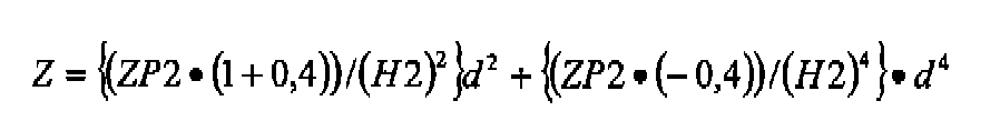 und einer zweiten Sinkbetragkurve, die repräsentiert ist durch:
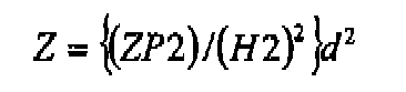
vorliegt, wobei:H2 der Abstand von dem Punkt P1 zu dem Punkt P2 gemessen in einer Richtung parallel zu der Nebenachse ist, ZP2 der Sinkbetrag in der Röhrenachsenrichtung bei dem Punkt P2 der Kurve C2 bezüglich des Punkts P1 ist und Z der Sinkbetrag in der Röhrenachsenrichtung bezüglich des Punkts P1 bei einem Punkt bei einem Abstand d von dem Punkt P1 in einer Richtung parallel zu der Unterachse ist. - Farbbildröhre nach Anspruch 1, bei der die Lochmaske (7) weiterhin so konfiguriert ist, dass:für eine Kurve C3, die auf der Oberfläche der Lochmaske (7) und in einer Ebene liegt, die durch die Mitte P0 der Lochmaske reicht und die parallel zu der Röhrenachse und einer Nebenachse der Lochmaske ist, dann zumindest 60 % der Sinkbetragkurve entlang der Kurve C3 zwischen der Mitte P0 und dem Nebenachsenende PS, wo die Kurve C3 das Ende des nutzbaren Bereichs der Lochmaske schneidet, auf einer Seite positioniert ist, wo ein Sinkbetrag größer als eine erste Sinkbetragkurve ist, die repräsentiert ist durch:wobei H3 der Abstand von der Mitte P0 zu dem Nebenachsenende PS gemessen in einer Richtung parallel zu der Unterachse ist, ZPS der Sinkbetrag in der Röhrenachsenrichtung bei dem Nebenachsenende PS der Kurve C3 bezüglich der Mitte P0 ist und Z der Sinkbetrag in der Röhrenachsenrichtung bezüglich der Mitte P0 bei einem Punkt bei einem Abstand d von der Mitte P0 in einer Richtung parallel zu der Nebenachse ist,

und die Lochmaske (7) weiterhin so konfiguriert ist, dass:für eine Kurve C4, die auf der Oberfläche der Lochmaske und in einer Ebene liegt, die durch das Hauptachsenende PL reicht und die parallel zu der Röhrenachse und einer Nebenachse der Lochmaske ist, dann zumindest 60 % der Sinkbetragkurve entlang der Kurve C4 zwischen dem Hauptachsenende PL und dem diagonalen Ende PD, wo die Kurve C4 eine diagonale Linie der Lochmaske schneidet, zwischen einer ersten Sinkbetragkurve, die repräsentiert ist durch:
und einer zweiten Sinkbetragkurve, die repräsentiert ist durch:
vorliegt, wobei H4 der Abstand von dem Hauptachsenende PL zu dem diagonalen Ende PD gemessen in einer Richtung parallel zu der Nebenachse ist, ZPD der Sinkbetrag in der Röhrenachsenrichtung bei dem diagonalen Ende PD der Kurve C4 bezüglich des Hauptachenendes PL ist und Z der Sinkbetrag in der Röhrenachsenrichtung bezüglich des Hauptachsenendes PL bei einem Punkt einen Abstand d von dem Hauptachsenende PL in einer Richtung parallel zu der Unterachse ist. - Farbbildröhre nach Anspruch 1, bei der die Lochmaske (7) so konfiguriert ist, dass die folgenden Formeln erfüllt sind:

und
wobei
D der Abstand von der Mitte P0 zu dem Ende des nutzbaren Bereichs der Lochmaske gemessen entlang einer diagonalen Achse der Lochmaske (7) ist, ZMD der Sinkbetrag in der Röhrenachsenrichtung bezüglich der Mitte P0 bei einem diagonalen Ende des nutzbaren Bereichs der Lochmaske ist, ZMH der Sinkbetrag in der Röhrenachsenrichtung bezüglich der Mitte P0 bei dem Hauptachsenende des nutzbaren Bereichs der Lochmaske ist und ZMV der Sinkbetrag in der Röhrenachsenrichtung bezüglich der Mitte P0 bei einem Nebenachsenende des nutzbaren Bereichs der Lochmaske (7) ist. - Farbbildröhre mit:einer Platte (3),einem Phosphor- bzw. Leuchtstoffbildschirm (5) in einer im wesentlichen rechteckigen Form, der auf einer inneren Oberfläche der Platte gebildet ist, wobei die Platte einen nutzbaren Bereich auf ihrer inneren Oberfläche hat, wo Leuchtstoffschichten von drei Farben gebildet sind, undeiner Lochmaske (7), in der eine Anzahl von Elektronenstrahldurchgangsöffnungen (6) gebildet ist, die so plaziert ist, um gegenüber dem Leuchtstoffbildschirm (5) zu sein,wobei ein Radius einer Krümmung einer äußeren Oberfläche der Platte (3) 10.000 mm oder mehr ist,die Lochmaske (7) aus einem Material gefertigt ist, das 95 % oder mehr Eisen enthält,die Farbbildröhre dadurch gekennzeichnet ist, dass die Platte (3) so konfiguriert ist, dass:für eine Kurve C1', die auf der inneren Oberfläche der Platte (3) und in einer Ebene liegt, die durch die Mitte P0' des nutzbaren Bereichs der Platte reicht und die parallel zu der Röhrenachse und einer Hauptachse der Platte ist, dann zumindest 60 % der Sinkbetragkurve entlang der Kurve C1' zwischen der Mitte P0' und dem Hauptachsenende PL', wo die Kurve C1' das Ende des nutzbaren Bereichs der inneren Oberfläche der Platte schneidet, zwischen einer ersten Sinkbetragkurve, die repräsentiert ist durch:

und einer zweiten Sinkbetragkurve, die repräsentiert ist durch:
vorliegt, wobei:W' der Abstand von der Mitte P0' zu dem Hauptachsenende PL' gemessen in einer Richtung parallel zu der Hauptachse ist, ZPL' der Sinkbetrag in der Röhrenachsenrichtung bei dem Hauptachsenende PL' der Kurve C1' bezüglich der Mitte P0' ist und Z' der Sinkbetrag in der Röhrenachsenrichtung bezüglich der Mitte P0' bei einem Punkt bei einem Abstand d' von der Mitte P0' in einer Richtung parallel zu der Hauptachse ist,und die Farbbildröhre weiterhin dadurch gekennzeichnet ist, dass die Platte (3) weiterhin so konfiguriert ist, dass:und einer zweiten Sinkbetragkurve, die repräsentiert ist durch:für eine Kurve C2' , die auf der inneren Oberfläche der Platte und in einer Ebene liegt, die durch einen Punkt P1' auf der inneren Oberfläche der Platte reicht und die parallel zu der Röhrenachse und einer Nebenachse der Platte ist, wobei der Punkt P1' auf der Kurve C1' bei einem Abstand 2/3 x W' gemessen in einer Richtung parallel zu der Hauptachse weg von der Mitte P0' liegt, dann zumindest 60 % der Sinkbetragkurve entlang der Kurve C2' zwischen dem Punkt P1' und einem Punkt P2', wo die Kurve C2' das Ende des nutzbaren Bereichs der inneren Oberfläche der Platte schneidet, zwischen einer ersten Sinkbetragkurve, die repräsentiert ist durch: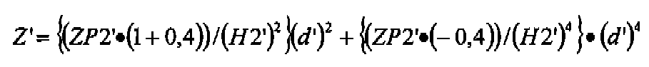

vorliegt, wobei:H2' der Abstand von dem Punkt P1' zu dem Punkt P2' gemessen in einer Richtung parallel zu der Unterachse ist, ZP2' der Sinkbetrag in der Röhrenachsenrichtung bei dem Punkt P2' der Kurve C2' bezüglich des Punkts P1' ist und Z' der Sinkbetrag in der Röhrenachsenrichtung bezüglich des Punkts P1' bei einem Punkt bei einem Abstand d' von dem Punkt P1' in einer Richtung parallel zu der Unterachse ist. - Farbbildröhre nach Anspruch 4, bei der die Platte (3) weiterhin so konfiguriert ist, dass:für eine Kurve C3', die auf der inneren Oberfläche der Platte (3) und in einer Ebene liegt, die durch die Mitte P0' der Platte reicht und die parallel zu der Röhrenachse und einer Nebenachse der Platte ist, dann zumindest 60 % der Sinkbetragkurve entlang der Kurve C3' zwischen der Mitte P0' und dem Nebenachsenende PS', wo die Kurve C3' das Ende des nutzbaren Bereichs der inneren Oberfläche der Platte schneidet, auf einer Seite positioniert ist, wo ein Sinkbetrag größer als eine erste Sinkbetragkurve ist, die repräsentiert ist durch:wobei H3' der Abstand von der Mitte P0' zu dem Nebenachsenende PS' gemessen in einer Richtung parallel zu der Nebenachse ist, ZPS' der Sinkbetrag in der Röhrenachsenrichtung bei dem Unterachsenende PS' der Kurve C3' bezüglich der Mitte P0' ist und Z' der Sinkbetrag in der Röhrenachsenrichtung bezüglich der Mitte P0' bei einem Punkt bei einem Abstand d' von der Mitte P0' in einer Richtung parallel zu der Nebenachse ist,

und die Platte (3) weiterhin so konfiguriert ist, dass:für eine Kurve C4', die auf der inneren Oberfläche der Platte (3) und in einer Ebene liegt, die durch das Hauptachsenende PL' reicht und die parallel zu der Röhrenachse und einer Nebenachse der Platte ist, dann zumindest 60 % der Sinkbetragkurve entlang der Kurve C4' zwischen dem Hauptachsenende PL' und dem diagonalen Ende PD', wo die Kurve C4' eine diagonale Linie der Platte schneidet, zwischen einer ersten Sinkbetragkurve, die repräsentiert ist durch:
und einer zweiten Sinkbetragkurve, die repräsentiert ist durch:
vorliegt, wobei H4' der Abstand von dem Hauptachsenende PL' zu dem diagonalen Ende PD' gemessen in einer Richtung parallel zu der Nebenachse ist, ZPD' der Sinkbetrag in der Röhrenachsenrichtung bei dem diagonalen Ende PD' der Kurve C4' bezüglich des Hauptachsenendes PL' ist und Z' der Sinkbetrag in der Röhrenachsenrichtung bezüglich des Hauptachsenendes PL' bei einem Punkt einen Abstand d' von dem Hauptachsenende PL' in einer Richtung parallel zu der Unterachse ist. - Farbbildröhre nach Anspruch 4, bei der:eine Transmittanz der Platte (3) bei der Mitte P0' 40 bis 60 % ist, undein Verhältnis: TD/TC < 2,1 erfüllt ist,wobei TC die Dicke der Platte (3) bei der Mitte P0' ist und TD die Dicke der Platte bei dem diagonalen Ende PD' des nutzbaren Bereichs der inneren Oberfläche der Platte (3) ist.
Applications Claiming Priority (1)
| Application Number | Priority Date | Filing Date | Title |
|---|---|---|---|
| JP2004163148 | 2004-06-01 |
Publications (2)
| Publication Number | Publication Date |
|---|---|
| EP1617455A1 EP1617455A1 (de) | 2006-01-18 |
| EP1617455B1 true EP1617455B1 (de) | 2007-08-01 |
Family
ID=34941517
Family Applications (1)
| Application Number | Title | Priority Date | Filing Date |
|---|---|---|---|
| EP05253331A Ceased EP1617455B1 (de) | 2004-06-01 | 2005-05-31 | Farbbildröhre |
Country Status (4)
| Country | Link |
|---|---|
| US (1) | US7045942B2 (de) |
| EP (1) | EP1617455B1 (de) |
| CN (1) | CN1320590C (de) |
| DE (1) | DE602005001816T2 (de) |
Families Citing this family (52)
| Publication number | Priority date | Publication date | Assignee | Title |
|---|---|---|---|---|
| JP2006049145A (ja) * | 2004-08-05 | 2006-02-16 | Matsushita Toshiba Picture Display Co Ltd | カラー受像管 |
| US20070126332A1 (en) * | 2005-12-02 | 2007-06-07 | Matsushita Toshiba Picture Display Co., Ltd. | Color picture tube |
| US8873585B2 (en) | 2006-12-19 | 2014-10-28 | Corning Optical Communications Wireless Ltd | Distributed antenna system for MIMO technologies |
| US20100054746A1 (en) | 2007-07-24 | 2010-03-04 | Eric Raymond Logan | Multi-port accumulator for radio-over-fiber (RoF) wireless picocellular systems |
| US8175459B2 (en) | 2007-10-12 | 2012-05-08 | Corning Cable Systems Llc | Hybrid wireless/wired RoF transponder and hybrid RoF communication system using same |
| WO2009081376A2 (en) | 2007-12-20 | 2009-07-02 | Mobileaccess Networks Ltd. | Extending outdoor location based services and applications into enclosed areas |
| EP2394379B1 (de) | 2009-02-03 | 2016-12-28 | Corning Optical Communications LLC | Verteilte antennensysteme auf glasfaserbasis, bestandteile und entsprechende verfahren zu ihrer kalibrierung |
| AU2010210766A1 (en) | 2009-02-03 | 2011-09-15 | Corning Cable Systems Llc | Optical fiber-based distributed antenna systems, components, and related methods for monitoring and configuring thereof |
| US9673904B2 (en) | 2009-02-03 | 2017-06-06 | Corning Optical Communications LLC | Optical fiber-based distributed antenna systems, components, and related methods for calibration thereof |
| US8548330B2 (en) | 2009-07-31 | 2013-10-01 | Corning Cable Systems Llc | Sectorization in distributed antenna systems, and related components and methods |
| US8280259B2 (en) | 2009-11-13 | 2012-10-02 | Corning Cable Systems Llc | Radio-over-fiber (RoF) system for protocol-independent wired and/or wireless communication |
| US8275265B2 (en) | 2010-02-15 | 2012-09-25 | Corning Cable Systems Llc | Dynamic cell bonding (DCB) for radio-over-fiber (RoF)-based networks and communication systems and related methods |
| US20110268446A1 (en) | 2010-05-02 | 2011-11-03 | Cune William P | Providing digital data services in optical fiber-based distributed radio frequency (rf) communications systems, and related components and methods |
| US9525488B2 (en) | 2010-05-02 | 2016-12-20 | Corning Optical Communications LLC | Digital data services and/or power distribution in optical fiber-based distributed communications systems providing digital data and radio frequency (RF) communications services, and related components and methods |
| EP2606707A1 (de) | 2010-08-16 | 2013-06-26 | Corning Cable Systems LLC | Remote-antennencluster und zugehörige systeme, bestandteile und verfahren zur unterstützung der signalverbreitung digitaler daten zwischen remote-antenneneinheiten |
| US9252874B2 (en) | 2010-10-13 | 2016-02-02 | Ccs Technology, Inc | Power management for remote antenna units in distributed antenna systems |
| CN203504582U (zh) | 2011-02-21 | 2014-03-26 | 康宁光缆系统有限责任公司 | 一种分布式天线系统及用于在其中分配电力的电源装置 |
| WO2012148940A1 (en) | 2011-04-29 | 2012-11-01 | Corning Cable Systems Llc | Systems, methods, and devices for increasing radio frequency (rf) power in distributed antenna systems |
| CN103548290B (zh) | 2011-04-29 | 2016-08-31 | 康宁光缆系统有限责任公司 | 判定分布式天线系统中的通信传播延迟及相关组件、系统与方法 |
| WO2013148986A1 (en) | 2012-03-30 | 2013-10-03 | Corning Cable Systems Llc | Reducing location-dependent interference in distributed antenna systems operating in multiple-input, multiple-output (mimo) configuration, and related components, systems, and methods |
| EP2842245A1 (de) | 2012-04-25 | 2015-03-04 | Corning Optical Communications LLC | Verteilte antennensystemarchitekturen |
| WO2014024192A1 (en) | 2012-08-07 | 2014-02-13 | Corning Mobile Access Ltd. | Distribution of time-division multiplexed (tdm) management services in a distributed antenna system, and related components, systems, and methods |
| US9455784B2 (en) | 2012-10-31 | 2016-09-27 | Corning Optical Communications Wireless Ltd | Deployable wireless infrastructures and methods of deploying wireless infrastructures |
| CN105308876B (zh) | 2012-11-29 | 2018-06-22 | 康宁光电通信有限责任公司 | 分布式天线系统中的远程单元天线结合 |
| US9647758B2 (en) | 2012-11-30 | 2017-05-09 | Corning Optical Communications Wireless Ltd | Cabling connectivity monitoring and verification |
| WO2014199384A1 (en) | 2013-06-12 | 2014-12-18 | Corning Optical Communications Wireless, Ltd. | Voltage controlled optical directional coupler |
| EP3008828B1 (de) | 2013-06-12 | 2017-08-09 | Corning Optical Communications Wireless Ltd. | Zeitduplexierung (tdd) in verteilten kommunikationssystemen, einschliesslich verteilten antennensystemen (dass) |
| US9247543B2 (en) | 2013-07-23 | 2016-01-26 | Corning Optical Communications Wireless Ltd | Monitoring non-supported wireless spectrum within coverage areas of distributed antenna systems (DASs) |
| US9661781B2 (en) | 2013-07-31 | 2017-05-23 | Corning Optical Communications Wireless Ltd | Remote units for distributed communication systems and related installation methods and apparatuses |
| US9385810B2 (en) | 2013-09-30 | 2016-07-05 | Corning Optical Communications Wireless Ltd | Connection mapping in distributed communication systems |
| US9178635B2 (en) | 2014-01-03 | 2015-11-03 | Corning Optical Communications Wireless Ltd | Separation of communication signal sub-bands in distributed antenna systems (DASs) to reduce interference |
| US9775123B2 (en) | 2014-03-28 | 2017-09-26 | Corning Optical Communications Wireless Ltd. | Individualized gain control of uplink paths in remote units in a distributed antenna system (DAS) based on individual remote unit contribution to combined uplink power |
| US9357551B2 (en) | 2014-05-30 | 2016-05-31 | Corning Optical Communications Wireless Ltd | Systems and methods for simultaneous sampling of serial digital data streams from multiple analog-to-digital converters (ADCS), including in distributed antenna systems |
| US9525472B2 (en) | 2014-07-30 | 2016-12-20 | Corning Incorporated | Reducing location-dependent destructive interference in distributed antenna systems (DASS) operating in multiple-input, multiple-output (MIMO) configuration, and related components, systems, and methods |
| US9730228B2 (en) | 2014-08-29 | 2017-08-08 | Corning Optical Communications Wireless Ltd | Individualized gain control of remote uplink band paths in a remote unit in a distributed antenna system (DAS), based on combined uplink power level in the remote unit |
| US9602210B2 (en) | 2014-09-24 | 2017-03-21 | Corning Optical Communications Wireless Ltd | Flexible head-end chassis supporting automatic identification and interconnection of radio interface modules and optical interface modules in an optical fiber-based distributed antenna system (DAS) |
| US9420542B2 (en) | 2014-09-25 | 2016-08-16 | Corning Optical Communications Wireless Ltd | System-wide uplink band gain control in a distributed antenna system (DAS), based on per band gain control of remote uplink paths in remote units |
| US10659163B2 (en) | 2014-09-25 | 2020-05-19 | Corning Optical Communications LLC | Supporting analog remote antenna units (RAUs) in digital distributed antenna systems (DASs) using analog RAU digital adaptors |
| WO2016071902A1 (en) | 2014-11-03 | 2016-05-12 | Corning Optical Communications Wireless Ltd. | Multi-band monopole planar antennas configured to facilitate improved radio frequency (rf) isolation in multiple-input multiple-output (mimo) antenna arrangement |
| WO2016075696A1 (en) | 2014-11-13 | 2016-05-19 | Corning Optical Communications Wireless Ltd. | Analog distributed antenna systems (dass) supporting distribution of digital communications signals interfaced from a digital signal source and analog radio frequency (rf) communications signals |
| US9729267B2 (en) | 2014-12-11 | 2017-08-08 | Corning Optical Communications Wireless Ltd | Multiplexing two separate optical links with the same wavelength using asymmetric combining and splitting |
| WO2016098111A1 (en) | 2014-12-18 | 2016-06-23 | Corning Optical Communications Wireless Ltd. | Digital- analog interface modules (da!ms) for flexibly.distributing digital and/or analog communications signals in wide-area analog distributed antenna systems (dass) |
| EP3235336A1 (de) | 2014-12-18 | 2017-10-25 | Corning Optical Communications Wireless Ltd. | Digitale schnittstellenmodule (dim) zur flexiblen verteilung digitaler und/oder analoger kommunikationssignale in wad-antennensystemen |
| US20160249365A1 (en) | 2015-02-19 | 2016-08-25 | Corning Optical Communications Wireless Ltd. | Offsetting unwanted downlink interference signals in an uplink path in a distributed antenna system (das) |
| US9681313B2 (en) | 2015-04-15 | 2017-06-13 | Corning Optical Communications Wireless Ltd | Optimizing remote antenna unit performance using an alternative data channel |
| US9948349B2 (en) | 2015-07-17 | 2018-04-17 | Corning Optical Communications Wireless Ltd | IOT automation and data collection system |
| US10560214B2 (en) | 2015-09-28 | 2020-02-11 | Corning Optical Communications LLC | Downlink and uplink communication path switching in a time-division duplex (TDD) distributed antenna system (DAS) |
| US10236924B2 (en) | 2016-03-31 | 2019-03-19 | Corning Optical Communications Wireless Ltd | Reducing out-of-channel noise in a wireless distribution system (WDS) |
| USD1044758S1 (en) * | 2023-07-26 | 2024-10-01 | Butterflymx, Inc. | Intercom display screen for recessed mount |
| USD1047952S1 (en) * | 2023-07-26 | 2024-10-22 | Butterflymx, Inc. | Intercom display screen for surface mount |
| USD1047953S1 (en) * | 2023-07-26 | 2024-10-22 | Butterflymx, Inc. | Intercom display screen for surface mount |
| USD1049071S1 (en) * | 2023-07-26 | 2024-10-29 | Butterflymx, Inc. | Intercom display screen for recessed mount |
Family Cites Families (20)
| Publication number | Priority date | Publication date | Assignee | Title |
|---|---|---|---|---|
| US4881004A (en) * | 1987-08-26 | 1989-11-14 | Kabushiki Kaisha Toshiba | Color cathode ray tube |
| JPH0614454B2 (ja) * | 1990-03-22 | 1994-02-23 | 松下電子工業株式会社 | シャドウマスク型カラー受像管 |
| IT1239510B (it) * | 1990-03-30 | 1993-11-03 | Videocolor Spa | Tubo a raggi catodici avente una lastra frontale perfezionata, con rapporto larghezza/altezza di 16/9" |
| ATE129598T1 (de) * | 1991-05-29 | 1995-11-15 | Philips Electronics Nv | Elektronenstrahlröhre mit bildfenster. |
| MY109452A (en) * | 1992-07-09 | 1997-01-31 | Toshiba Kk | Color cathode ray tube |
| TW297907B (de) * | 1994-07-14 | 1997-02-11 | Toshiba Co Ltd | |
| JPH10199436A (ja) | 1997-01-13 | 1998-07-31 | Toshiba Corp | カラー受像管およびその製造方法 |
| US6025676A (en) * | 1996-03-06 | 2000-02-15 | Kabushiki Kaisha Toshiba | Cathode ray tube having improved curvature characteristics and method of fabrication thereof |
| EP0933797B1 (de) * | 1998-01-30 | 2004-07-28 | Hitachi, Ltd. | Kathodenstrahlröhre |
| TW430851B (en) * | 1998-09-17 | 2001-04-21 | Toshiba Corp | Color picture tube |
| US6465945B1 (en) * | 1999-06-16 | 2002-10-15 | Kabushiki Kaisha Toshiba | Color cathode-ray tube |
| JP2001101984A (ja) * | 1999-09-30 | 2001-04-13 | Hitachi Ltd | カラー陰極線管 |
| KR100331820B1 (ko) * | 2000-04-12 | 2002-04-09 | 구자홍 | 평면 음극선관 |
| JP2002245948A (ja) * | 2001-02-15 | 2002-08-30 | Toshiba Corp | カラー受像管 |
| US6590327B2 (en) * | 2001-05-01 | 2003-07-08 | Hitachi Ltd. | Color cathode ray tube having flat outer face |
| KR100426575B1 (ko) * | 2001-05-10 | 2004-04-08 | 엘지전자 주식회사 | 음극선관용 패널 구조 |
| CN1385873A (zh) * | 2001-05-10 | 2002-12-18 | 株式会社日立制作所 | 具有平的外表面的彩色阴极射线管 |
| KR100408005B1 (ko) * | 2002-01-03 | 2003-12-03 | 엘지.필립스디스플레이(주) | 마스크 스트레칭형 칼라 음극선관용 패널 |
| KR100443611B1 (ko) | 2002-06-26 | 2004-08-09 | 엘지.필립스디스플레이(주) | 음극선관용 패널 |
| KR20060000514A (ko) * | 2004-06-29 | 2006-01-06 | 삼성에스디아이 주식회사 | 음극선관 |
-
2005
- 2005-05-31 DE DE602005001816T patent/DE602005001816T2/de not_active Expired - Fee Related
- 2005-05-31 EP EP05253331A patent/EP1617455B1/de not_active Ceased
- 2005-06-01 CN CNB2005100754279A patent/CN1320590C/zh not_active Expired - Fee Related
- 2005-06-01 US US11/142,135 patent/US7045942B2/en not_active Expired - Fee Related
Also Published As
| Publication number | Publication date |
|---|---|
| DE602005001816T2 (de) | 2007-12-06 |
| DE602005001816D1 (de) | 2007-09-13 |
| US20050269930A1 (en) | 2005-12-08 |
| EP1617455A1 (de) | 2006-01-18 |
| US7045942B2 (en) | 2006-05-16 |
| CN1705069A (zh) | 2005-12-07 |
| CN1320590C (zh) | 2007-06-06 |
Similar Documents
| Publication | Publication Date | Title |
|---|---|---|
| EP1617455B1 (de) | Farbbildröhre | |
| EP0655762B1 (de) | Farbkathodenstrahlröhre | |
| EP0881658B1 (de) | Schattenmaske und Farbkathodenstrahlröre | |
| EP0578251B1 (de) | Farbbildkathodenstrahlröhre | |
| KR20000035225A (ko) | 칼라음극선관 | |
| KR100409131B1 (ko) | 칼라음극선관 | |
| US7012356B2 (en) | Color cathode ray tube | |
| KR20050003153A (ko) | 음극선관 | |
| JP2001060443A (ja) | カラー陰極線管 | |
| US7265484B2 (en) | Color picture tube with curved shadow mask | |
| US6707242B2 (en) | Color cathode ray tube | |
| US6600258B2 (en) | Tension mask for a cathode-ray-tube | |
| KR100662942B1 (ko) | 음극선관 | |
| EP1369893B1 (de) | Schattenmaske für eine Kathodenstrahlröhre | |
| JP4025785B2 (ja) | カラー受像管 | |
| KR100532067B1 (ko) | 칼라 음극선관 | |
| KR100443612B1 (ko) | 음극선관용 새도우 마스크 | |
| KR100447657B1 (ko) | 상하주사형 칼라음극선관 | |
| US20070018556A1 (en) | Color picture tube | |
| US6166482A (en) | Shadow mask structure with specific skirt portion | |
| US6756725B2 (en) | Cathode ray tube with tension mask | |
| US20060066207A1 (en) | Color picture tube | |
| JP2006260979A (ja) | カラー受像管 | |
| JP2007188786A (ja) | カラー受像管 | |
| JPH07122205A (ja) | カラー受像管 |
Legal Events
| Date | Code | Title | Description |
|---|---|---|---|
| PUAI | Public reference made under article 153(3) epc to a published international application that has entered the european phase |
Free format text: ORIGINAL CODE: 0009012 |
|
| 17P | Request for examination filed |
Effective date: 20050627 |
|
| AK | Designated contracting states |
Kind code of ref document: A1 Designated state(s): AT BE BG CH CY CZ DE DK EE ES FI FR GB GR HU IE IS IT LI LT LU MC NL PL PT RO SE SI SK TR |
|
| AX | Request for extension of the european patent |
Extension state: AL BA HR LV MK YU |
|
| AKX | Designation fees paid |
Designated state(s): DE FR GB IT |
|
| GRAP | Despatch of communication of intention to grant a patent |
Free format text: ORIGINAL CODE: EPIDOSNIGR1 |
|
| RIN1 | Information on inventor provided before grant (corrected) |
Inventor name: UCHIKAWA, TOSHIO Inventor name: NIHEI, FUMIAKI Inventor name: SHIMIZU, NORIO |
|
| GRAS | Grant fee paid |
Free format text: ORIGINAL CODE: EPIDOSNIGR3 |
|
| GRAA | (expected) grant |
Free format text: ORIGINAL CODE: 0009210 |
|
| AK | Designated contracting states |
Kind code of ref document: B1 Designated state(s): DE FR GB IT |
|
| REG | Reference to a national code |
Ref country code: GB Ref legal event code: FG4D |
|
| REF | Corresponds to: |
Ref document number: 602005001816 Country of ref document: DE Date of ref document: 20070913 Kind code of ref document: P |
|
| EN | Fr: translation not filed | ||
| PLBE | No opposition filed within time limit |
Free format text: ORIGINAL CODE: 0009261 |
|
| STAA | Information on the status of an ep patent application or granted ep patent |
Free format text: STATUS: NO OPPOSITION FILED WITHIN TIME LIMIT |
|
| 26N | No opposition filed |
Effective date: 20080506 |
|
| PG25 | Lapsed in a contracting state [announced via postgrant information from national office to epo] |
Ref country code: FR Free format text: LAPSE BECAUSE OF FAILURE TO SUBMIT A TRANSLATION OF THE DESCRIPTION OR TO PAY THE FEE WITHIN THE PRESCRIBED TIME-LIMIT Effective date: 20080328 |
|
| PG25 | Lapsed in a contracting state [announced via postgrant information from national office to epo] |
Ref country code: DE Free format text: LAPSE BECAUSE OF NON-PAYMENT OF DUE FEES Effective date: 20081202 |
|
| GBPC | Gb: european patent ceased through non-payment of renewal fee |
Effective date: 20090531 |
|
| PG25 | Lapsed in a contracting state [announced via postgrant information from national office to epo] |
Ref country code: GB Free format text: LAPSE BECAUSE OF NON-PAYMENT OF DUE FEES Effective date: 20090531 |
|
| PG25 | Lapsed in a contracting state [announced via postgrant information from national office to epo] |
Ref country code: IT Free format text: LAPSE BECAUSE OF NON-PAYMENT OF DUE FEES Effective date: 20080531 |