EP1614460A1 - Substrat pour biopuces - Google Patents
Substrat pour biopuces Download PDFInfo
- Publication number
- EP1614460A1 EP1614460A1 EP04291742A EP04291742A EP1614460A1 EP 1614460 A1 EP1614460 A1 EP 1614460A1 EP 04291742 A EP04291742 A EP 04291742A EP 04291742 A EP04291742 A EP 04291742A EP 1614460 A1 EP1614460 A1 EP 1614460A1
- Authority
- EP
- European Patent Office
- Prior art keywords
- substrate
- layer
- dna
- reaction region
- bottomed
- Prior art date
- Legal status (The legal status is an assumption and is not a legal conclusion. Google has not performed a legal analysis and makes no representation as to the accuracy of the status listed.)
- Withdrawn
Links
- 239000000758 substrate Substances 0.000 title claims abstract description 162
- 238000000018 DNA microarray Methods 0.000 title claims abstract description 53
- 238000006243 chemical reaction Methods 0.000 claims abstract description 79
- 239000000126 substance Substances 0.000 claims abstract description 53
- 239000000463 material Substances 0.000 claims abstract description 30
- 239000011521 glass Substances 0.000 claims description 6
- 239000010410 layer Substances 0.000 description 106
- 108020004414 DNA Proteins 0.000 description 88
- 102000053602 DNA Human genes 0.000 description 88
- 239000000523 sample Substances 0.000 description 42
- 229920005989 resin Polymers 0.000 description 35
- 239000011347 resin Substances 0.000 description 35
- 108091034117 Oligonucleotide Proteins 0.000 description 34
- 238000000034 method Methods 0.000 description 27
- JLCPHMBAVCMARE-UHFFFAOYSA-N [3-[[3-[[3-[[3-[[3-[[3-[[3-[[3-[[3-[[3-[[3-[[5-(2-amino-6-oxo-1H-purin-9-yl)-3-[[3-[[3-[[3-[[3-[[3-[[5-(2-amino-6-oxo-1H-purin-9-yl)-3-[[5-(2-amino-6-oxo-1H-purin-9-yl)-3-hydroxyoxolan-2-yl]methoxy-hydroxyphosphoryl]oxyoxolan-2-yl]methoxy-hydroxyphosphoryl]oxy-5-(5-methyl-2,4-dioxopyrimidin-1-yl)oxolan-2-yl]methoxy-hydroxyphosphoryl]oxy-5-(6-aminopurin-9-yl)oxolan-2-yl]methoxy-hydroxyphosphoryl]oxy-5-(6-aminopurin-9-yl)oxolan-2-yl]methoxy-hydroxyphosphoryl]oxy-5-(6-aminopurin-9-yl)oxolan-2-yl]methoxy-hydroxyphosphoryl]oxy-5-(6-aminopurin-9-yl)oxolan-2-yl]methoxy-hydroxyphosphoryl]oxyoxolan-2-yl]methoxy-hydroxyphosphoryl]oxy-5-(5-methyl-2,4-dioxopyrimidin-1-yl)oxolan-2-yl]methoxy-hydroxyphosphoryl]oxy-5-(4-amino-2-oxopyrimidin-1-yl)oxolan-2-yl]methoxy-hydroxyphosphoryl]oxy-5-(5-methyl-2,4-dioxopyrimidin-1-yl)oxolan-2-yl]methoxy-hydroxyphosphoryl]oxy-5-(5-methyl-2,4-dioxopyrimidin-1-yl)oxolan-2-yl]methoxy-hydroxyphosphoryl]oxy-5-(6-aminopurin-9-yl)oxolan-2-yl]methoxy-hydroxyphosphoryl]oxy-5-(6-aminopurin-9-yl)oxolan-2-yl]methoxy-hydroxyphosphoryl]oxy-5-(4-amino-2-oxopyrimidin-1-yl)oxolan-2-yl]methoxy-hydroxyphosphoryl]oxy-5-(4-amino-2-oxopyrimidin-1-yl)oxolan-2-yl]methoxy-hydroxyphosphoryl]oxy-5-(4-amino-2-oxopyrimidin-1-yl)oxolan-2-yl]methoxy-hydroxyphosphoryl]oxy-5-(6-aminopurin-9-yl)oxolan-2-yl]methoxy-hydroxyphosphoryl]oxy-5-(4-amino-2-oxopyrimidin-1-yl)oxolan-2-yl]methyl [5-(6-aminopurin-9-yl)-2-(hydroxymethyl)oxolan-3-yl] hydrogen phosphate Polymers Cc1cn(C2CC(OP(O)(=O)OCC3OC(CC3OP(O)(=O)OCC3OC(CC3O)n3cnc4c3nc(N)[nH]c4=O)n3cnc4c3nc(N)[nH]c4=O)C(COP(O)(=O)OC3CC(OC3COP(O)(=O)OC3CC(OC3COP(O)(=O)OC3CC(OC3COP(O)(=O)OC3CC(OC3COP(O)(=O)OC3CC(OC3COP(O)(=O)OC3CC(OC3COP(O)(=O)OC3CC(OC3COP(O)(=O)OC3CC(OC3COP(O)(=O)OC3CC(OC3COP(O)(=O)OC3CC(OC3COP(O)(=O)OC3CC(OC3COP(O)(=O)OC3CC(OC3COP(O)(=O)OC3CC(OC3COP(O)(=O)OC3CC(OC3COP(O)(=O)OC3CC(OC3COP(O)(=O)OC3CC(OC3COP(O)(=O)OC3CC(OC3CO)n3cnc4c(N)ncnc34)n3ccc(N)nc3=O)n3cnc4c(N)ncnc34)n3ccc(N)nc3=O)n3ccc(N)nc3=O)n3ccc(N)nc3=O)n3cnc4c(N)ncnc34)n3cnc4c(N)ncnc34)n3cc(C)c(=O)[nH]c3=O)n3cc(C)c(=O)[nH]c3=O)n3ccc(N)nc3=O)n3cc(C)c(=O)[nH]c3=O)n3cnc4c3nc(N)[nH]c4=O)n3cnc4c(N)ncnc34)n3cnc4c(N)ncnc34)n3cnc4c(N)ncnc34)n3cnc4c(N)ncnc34)O2)c(=O)[nH]c1=O JLCPHMBAVCMARE-UHFFFAOYSA-N 0.000 description 22
- 238000003786 synthesis reaction Methods 0.000 description 22
- 150000008300 phosphoramidites Chemical class 0.000 description 20
- 125000006850 spacer group Chemical group 0.000 description 19
- BLRPTPMANUNPDV-UHFFFAOYSA-N Silane Chemical compound [SiH4] BLRPTPMANUNPDV-UHFFFAOYSA-N 0.000 description 16
- 230000015572 biosynthetic process Effects 0.000 description 16
- 229910000077 silane Inorganic materials 0.000 description 16
- 230000002194 synthesizing effect Effects 0.000 description 14
- 238000005530 etching Methods 0.000 description 13
- 108090000623 proteins and genes Proteins 0.000 description 8
- 102000004169 proteins and genes Human genes 0.000 description 7
- 239000002585 base Substances 0.000 description 6
- 230000002779 inactivation Effects 0.000 description 6
- 239000007788 liquid Substances 0.000 description 6
- 238000000206 photolithography Methods 0.000 description 6
- 239000010409 thin film Substances 0.000 description 6
- 238000004040 coloring Methods 0.000 description 5
- 238000013461 design Methods 0.000 description 5
- 238000010586 diagram Methods 0.000 description 5
- 125000002887 hydroxy group Chemical group [H]O* 0.000 description 5
- 235000000346 sugar Nutrition 0.000 description 5
- 230000006820 DNA synthesis Effects 0.000 description 4
- 239000002253 acid Substances 0.000 description 4
- OPTASPLRGRRNAP-UHFFFAOYSA-N cytosine Chemical compound NC=1C=CNC(=O)N=1 OPTASPLRGRRNAP-UHFFFAOYSA-N 0.000 description 4
- -1 dimethoxytrityl Chemical group 0.000 description 4
- 230000002209 hydrophobic effect Effects 0.000 description 4
- 239000003960 organic solvent Substances 0.000 description 4
- 229920002477 rna polymer Polymers 0.000 description 4
- RWQNBRDOKXIBIV-UHFFFAOYSA-N thymine Chemical compound CC1=CNC(=O)NC1=O RWQNBRDOKXIBIV-UHFFFAOYSA-N 0.000 description 4
- WFDIJRYMOXRFFG-UHFFFAOYSA-N Acetic anhydride Chemical compound CC(=O)OC(C)=O WFDIJRYMOXRFFG-UHFFFAOYSA-N 0.000 description 3
- HEMHJVSKTPXQMS-UHFFFAOYSA-M Sodium hydroxide Chemical compound [OH-].[Na+] HEMHJVSKTPXQMS-UHFFFAOYSA-M 0.000 description 3
- 239000003513 alkali Substances 0.000 description 3
- 230000000295 complement effect Effects 0.000 description 3
- 230000003647 oxidation Effects 0.000 description 3
- 238000007254 oxidation reaction Methods 0.000 description 3
- 229910052760 oxygen Inorganic materials 0.000 description 3
- 239000001301 oxygen Substances 0.000 description 3
- 108090000765 processed proteins & peptides Proteins 0.000 description 3
- 102000004196 processed proteins & peptides Human genes 0.000 description 3
- 238000002444 silanisation Methods 0.000 description 3
- 150000008163 sugars Chemical class 0.000 description 3
- 238000012360 testing method Methods 0.000 description 3
- 238000013519 translation Methods 0.000 description 3
- 229910052581 Si3N4 Inorganic materials 0.000 description 2
- XUIMIQQOPSSXEZ-UHFFFAOYSA-N Silicon Chemical compound [Si] XUIMIQQOPSSXEZ-UHFFFAOYSA-N 0.000 description 2
- WYURNTSHIVDZCO-UHFFFAOYSA-N Tetrahydrofuran Chemical compound C1CCOC1 WYURNTSHIVDZCO-UHFFFAOYSA-N 0.000 description 2
- 125000003277 amino group Chemical group 0.000 description 2
- 125000003178 carboxy group Chemical group [H]OC(*)=O 0.000 description 2
- 239000003153 chemical reaction reagent Substances 0.000 description 2
- 239000003795 chemical substances by application Substances 0.000 description 2
- 229940104302 cytosine Drugs 0.000 description 2
- 238000001514 detection method Methods 0.000 description 2
- 125000000524 functional group Chemical group 0.000 description 2
- UYTPUPDQBNUYGX-UHFFFAOYSA-N guanine Chemical compound O=C1NC(N)=NC2=C1N=CN2 UYTPUPDQBNUYGX-UHFFFAOYSA-N 0.000 description 2
- 150000004767 nitrides Chemical class 0.000 description 2
- BASFCYQUMIYNBI-UHFFFAOYSA-N platinum Chemical compound [Pt] BASFCYQUMIYNBI-UHFFFAOYSA-N 0.000 description 2
- 229910052710 silicon Inorganic materials 0.000 description 2
- 239000010703 silicon Substances 0.000 description 2
- HQVNEWCFYHHQES-UHFFFAOYSA-N silicon nitride Chemical compound N12[Si]34N5[Si]62N3[Si]51N64 HQVNEWCFYHHQES-UHFFFAOYSA-N 0.000 description 2
- 239000007858 starting material Substances 0.000 description 2
- 239000002344 surface layer Substances 0.000 description 2
- 125000003396 thiol group Chemical group [H]S* 0.000 description 2
- 229940113082 thymine Drugs 0.000 description 2
- YNJBWRMUSHSURL-UHFFFAOYSA-N trichloroacetic acid Chemical compound OC(=O)C(Cl)(Cl)Cl YNJBWRMUSHSURL-UHFFFAOYSA-N 0.000 description 2
- 229930024421 Adenine Natural products 0.000 description 1
- GFFGJBXGBJISGV-UHFFFAOYSA-N Adenine Chemical compound NC1=NC=NC2=C1N=CN2 GFFGJBXGBJISGV-UHFFFAOYSA-N 0.000 description 1
- 102000004190 Enzymes Human genes 0.000 description 1
- 108090000790 Enzymes Proteins 0.000 description 1
- 102000004856 Lectins Human genes 0.000 description 1
- 108090001090 Lectins Proteins 0.000 description 1
- 206010067482 No adverse event Diseases 0.000 description 1
- 239000004698 Polyethylene Substances 0.000 description 1
- 239000004793 Polystyrene Substances 0.000 description 1
- 239000006087 Silane Coupling Agent Substances 0.000 description 1
- 102000040945 Transcription factor Human genes 0.000 description 1
- 108091023040 Transcription factor Proteins 0.000 description 1
- 230000004913 activation Effects 0.000 description 1
- 239000013543 active substance Substances 0.000 description 1
- 229960000643 adenine Drugs 0.000 description 1
- 150000001343 alkyl silanes Chemical class 0.000 description 1
- QVGXLLKOCUKJST-UHFFFAOYSA-N atomic oxygen Chemical compound [O] QVGXLLKOCUKJST-UHFFFAOYSA-N 0.000 description 1
- 239000012472 biological sample Substances 0.000 description 1
- 230000000903 blocking effect Effects 0.000 description 1
- 239000008280 blood Substances 0.000 description 1
- 210000004369 blood Anatomy 0.000 description 1
- 230000008878 coupling Effects 0.000 description 1
- 238000010168 coupling process Methods 0.000 description 1
- 238000005859 coupling reaction Methods 0.000 description 1
- 238000006642 detritylation reaction Methods 0.000 description 1
- 238000004090 dissolution Methods 0.000 description 1
- 238000001312 dry etching Methods 0.000 description 1
- 230000002124 endocrine Effects 0.000 description 1
- 125000003700 epoxy group Chemical group 0.000 description 1
- 239000003822 epoxy resin Substances 0.000 description 1
- 239000010408 film Substances 0.000 description 1
- 239000005556 hormone Substances 0.000 description 1
- 229940088597 hormone Drugs 0.000 description 1
- 230000007062 hydrolysis Effects 0.000 description 1
- 238000006460 hydrolysis reaction Methods 0.000 description 1
- 239000012212 insulator Substances 0.000 description 1
- 239000002523 lectin Substances 0.000 description 1
- 150000002632 lipids Chemical class 0.000 description 1
- 238000004519 manufacturing process Methods 0.000 description 1
- 230000000873 masking effect Effects 0.000 description 1
- 229910052751 metal Inorganic materials 0.000 description 1
- 239000002184 metal Substances 0.000 description 1
- 150000002739 metals Chemical class 0.000 description 1
- 238000002493 microarray Methods 0.000 description 1
- 229910021421 monocrystalline silicon Inorganic materials 0.000 description 1
- 239000000178 monomer Substances 0.000 description 1
- 102000039446 nucleic acids Human genes 0.000 description 1
- 108020004707 nucleic acids Proteins 0.000 description 1
- 150000007523 nucleic acids Chemical class 0.000 description 1
- 238000001020 plasma etching Methods 0.000 description 1
- 239000004033 plastic Substances 0.000 description 1
- 229920003023 plastic Polymers 0.000 description 1
- 229910052697 platinum Inorganic materials 0.000 description 1
- 229920000647 polyepoxide Polymers 0.000 description 1
- 229920000573 polyethylene Polymers 0.000 description 1
- 238000006116 polymerization reaction Methods 0.000 description 1
- 102000040430 polynucleotide Human genes 0.000 description 1
- 108091033319 polynucleotide Proteins 0.000 description 1
- 239000002157 polynucleotide Substances 0.000 description 1
- 229920002223 polystyrene Polymers 0.000 description 1
- 239000010453 quartz Substances 0.000 description 1
- 238000000926 separation method Methods 0.000 description 1
- SCPYDCQAZCOKTP-UHFFFAOYSA-N silanol Chemical compound [SiH3]O SCPYDCQAZCOKTP-UHFFFAOYSA-N 0.000 description 1
- VYPSYNLAJGMNEJ-UHFFFAOYSA-N silicon dioxide Inorganic materials O=[Si]=O VYPSYNLAJGMNEJ-UHFFFAOYSA-N 0.000 description 1
- 238000000992 sputter etching Methods 0.000 description 1
- YLQBMQCUIZJEEH-UHFFFAOYSA-N tetrahydrofuran Natural products C=1C=COC=1 YLQBMQCUIZJEEH-UHFFFAOYSA-N 0.000 description 1
- 125000002088 tosyl group Chemical group [H]C1=C([H])C(=C([H])C([H])=C1C([H])([H])[H])S(*)(=O)=O 0.000 description 1
- 238000001771 vacuum deposition Methods 0.000 description 1
- 239000012808 vapor phase Substances 0.000 description 1
- 239000011782 vitamin Substances 0.000 description 1
- 229940088594 vitamin Drugs 0.000 description 1
- 229930003231 vitamin Natural products 0.000 description 1
- 235000013343 vitamin Nutrition 0.000 description 1
- 238000001039 wet etching Methods 0.000 description 1
Images


Classifications
-
- B—PERFORMING OPERATIONS; TRANSPORTING
- B01—PHYSICAL OR CHEMICAL PROCESSES OR APPARATUS IN GENERAL
- B01J—CHEMICAL OR PHYSICAL PROCESSES, e.g. CATALYSIS OR COLLOID CHEMISTRY; THEIR RELEVANT APPARATUS
- B01J19/00—Chemical, physical or physico-chemical processes in general; Their relevant apparatus
- B01J19/0046—Sequential or parallel reactions, e.g. for the synthesis of polypeptides or polynucleotides; Apparatus and devices for combinatorial chemistry or for making molecular arrays
-
- B—PERFORMING OPERATIONS; TRANSPORTING
- B01—PHYSICAL OR CHEMICAL PROCESSES OR APPARATUS IN GENERAL
- B01L—CHEMICAL OR PHYSICAL LABORATORY APPARATUS FOR GENERAL USE
- B01L3/00—Containers or dishes for laboratory use, e.g. laboratory glassware; Droppers
- B01L3/50—Containers for the purpose of retaining a material to be analysed, e.g. test tubes
- B01L3/508—Containers for the purpose of retaining a material to be analysed, e.g. test tubes rigid containers not provided for above
- B01L3/5085—Containers for the purpose of retaining a material to be analysed, e.g. test tubes rigid containers not provided for above for multiple samples, e.g. microtitration plates
-
- B—PERFORMING OPERATIONS; TRANSPORTING
- B01—PHYSICAL OR CHEMICAL PROCESSES OR APPARATUS IN GENERAL
- B01J—CHEMICAL OR PHYSICAL PROCESSES, e.g. CATALYSIS OR COLLOID CHEMISTRY; THEIR RELEVANT APPARATUS
- B01J2219/00—Chemical, physical or physico-chemical processes in general; Their relevant apparatus
- B01J2219/00274—Sequential or parallel reactions; Apparatus and devices for combinatorial chemistry or for making arrays; Chemical library technology
- B01J2219/00277—Apparatus
- B01J2219/00279—Features relating to reactor vessels
- B01J2219/00306—Reactor vessels in a multiple arrangement
- B01J2219/00313—Reactor vessels in a multiple arrangement the reactor vessels being formed by arrays of wells in blocks
- B01J2219/00315—Microtiter plates
- B01J2219/00317—Microwell devices, i.e. having large numbers of wells
-
- B—PERFORMING OPERATIONS; TRANSPORTING
- B01—PHYSICAL OR CHEMICAL PROCESSES OR APPARATUS IN GENERAL
- B01J—CHEMICAL OR PHYSICAL PROCESSES, e.g. CATALYSIS OR COLLOID CHEMISTRY; THEIR RELEVANT APPARATUS
- B01J2219/00—Chemical, physical or physico-chemical processes in general; Their relevant apparatus
- B01J2219/00274—Sequential or parallel reactions; Apparatus and devices for combinatorial chemistry or for making arrays; Chemical library technology
- B01J2219/00583—Features relative to the processes being carried out
- B01J2219/00603—Making arrays on substantially continuous surfaces
- B01J2219/00605—Making arrays on substantially continuous surfaces the compounds being directly bound or immobilised to solid supports
- B01J2219/00612—Making arrays on substantially continuous surfaces the compounds being directly bound or immobilised to solid supports the surface being inorganic
-
- B—PERFORMING OPERATIONS; TRANSPORTING
- B01—PHYSICAL OR CHEMICAL PROCESSES OR APPARATUS IN GENERAL
- B01J—CHEMICAL OR PHYSICAL PROCESSES, e.g. CATALYSIS OR COLLOID CHEMISTRY; THEIR RELEVANT APPARATUS
- B01J2219/00—Chemical, physical or physico-chemical processes in general; Their relevant apparatus
- B01J2219/00274—Sequential or parallel reactions; Apparatus and devices for combinatorial chemistry or for making arrays; Chemical library technology
- B01J2219/00583—Features relative to the processes being carried out
- B01J2219/00603—Making arrays on substantially continuous surfaces
- B01J2219/00605—Making arrays on substantially continuous surfaces the compounds being directly bound or immobilised to solid supports
- B01J2219/00614—Delimitation of the attachment areas
- B01J2219/00617—Delimitation of the attachment areas by chemical means
-
- B—PERFORMING OPERATIONS; TRANSPORTING
- B01—PHYSICAL OR CHEMICAL PROCESSES OR APPARATUS IN GENERAL
- B01J—CHEMICAL OR PHYSICAL PROCESSES, e.g. CATALYSIS OR COLLOID CHEMISTRY; THEIR RELEVANT APPARATUS
- B01J2219/00—Chemical, physical or physico-chemical processes in general; Their relevant apparatus
- B01J2219/00274—Sequential or parallel reactions; Apparatus and devices for combinatorial chemistry or for making arrays; Chemical library technology
- B01J2219/00583—Features relative to the processes being carried out
- B01J2219/00603—Making arrays on substantially continuous surfaces
- B01J2219/00605—Making arrays on substantially continuous surfaces the compounds being directly bound or immobilised to solid supports
- B01J2219/00614—Delimitation of the attachment areas
- B01J2219/00621—Delimitation of the attachment areas by physical means, e.g. trenches, raised areas
-
- B—PERFORMING OPERATIONS; TRANSPORTING
- B01—PHYSICAL OR CHEMICAL PROCESSES OR APPARATUS IN GENERAL
- B01J—CHEMICAL OR PHYSICAL PROCESSES, e.g. CATALYSIS OR COLLOID CHEMISTRY; THEIR RELEVANT APPARATUS
- B01J2219/00—Chemical, physical or physico-chemical processes in general; Their relevant apparatus
- B01J2219/00274—Sequential or parallel reactions; Apparatus and devices for combinatorial chemistry or for making arrays; Chemical library technology
- B01J2219/00583—Features relative to the processes being carried out
- B01J2219/00603—Making arrays on substantially continuous surfaces
- B01J2219/00605—Making arrays on substantially continuous surfaces the compounds being directly bound or immobilised to solid supports
- B01J2219/00623—Immobilisation or binding
- B01J2219/00626—Covalent
-
- B—PERFORMING OPERATIONS; TRANSPORTING
- B01—PHYSICAL OR CHEMICAL PROCESSES OR APPARATUS IN GENERAL
- B01J—CHEMICAL OR PHYSICAL PROCESSES, e.g. CATALYSIS OR COLLOID CHEMISTRY; THEIR RELEVANT APPARATUS
- B01J2219/00—Chemical, physical or physico-chemical processes in general; Their relevant apparatus
- B01J2219/00274—Sequential or parallel reactions; Apparatus and devices for combinatorial chemistry or for making arrays; Chemical library technology
- B01J2219/00583—Features relative to the processes being carried out
- B01J2219/00603—Making arrays on substantially continuous surfaces
- B01J2219/00605—Making arrays on substantially continuous surfaces the compounds being directly bound or immobilised to solid supports
- B01J2219/00632—Introduction of reactive groups to the surface
- B01J2219/00637—Introduction of reactive groups to the surface by coating it with another layer
-
- B—PERFORMING OPERATIONS; TRANSPORTING
- B01—PHYSICAL OR CHEMICAL PROCESSES OR APPARATUS IN GENERAL
- B01L—CHEMICAL OR PHYSICAL LABORATORY APPARATUS FOR GENERAL USE
- B01L2200/00—Solutions for specific problems relating to chemical or physical laboratory apparatus
- B01L2200/12—Specific details about manufacturing devices
-
- B—PERFORMING OPERATIONS; TRANSPORTING
- B01—PHYSICAL OR CHEMICAL PROCESSES OR APPARATUS IN GENERAL
- B01L—CHEMICAL OR PHYSICAL LABORATORY APPARATUS FOR GENERAL USE
- B01L2300/00—Additional constructional details
- B01L2300/08—Geometry, shape and general structure
- B01L2300/0809—Geometry, shape and general structure rectangular shaped
- B01L2300/0819—Microarrays; Biochips
-
- B—PERFORMING OPERATIONS; TRANSPORTING
- B01—PHYSICAL OR CHEMICAL PROCESSES OR APPARATUS IN GENERAL
- B01L—CHEMICAL OR PHYSICAL LABORATORY APPARATUS FOR GENERAL USE
- B01L2300/00—Additional constructional details
- B01L2300/08—Geometry, shape and general structure
- B01L2300/0887—Laminated structure
-
- C—CHEMISTRY; METALLURGY
- C40—COMBINATORIAL TECHNOLOGY
- C40B—COMBINATORIAL CHEMISTRY; LIBRARIES, e.g. CHEMICAL LIBRARIES
- C40B60/00—Apparatus specially adapted for use in combinatorial chemistry or with libraries
- C40B60/14—Apparatus specially adapted for use in combinatorial chemistry or with libraries for creating libraries
Definitions
- the invention relates to a substrate for biochips, more specifically a substrate used for making a biochip having biological substances fixed at predetermined positions on a substrate and used for obtaining information about various biological samples to be examined.
- the invention relates in particular to a substrate for biochips suitable for making a DNA chip by chemically synthesizing probe DNA directly on a substrate.
- Biochip is the generic term for devices in which biological substances that chemically react with to-be-detected biological substances in a specific manner are fixed at predetermined positions on a chip surface.
- a DNA chip that is a typical example of the biochip is used to detect the types and amounts of target DNA included in blood or cell extract.
- the DNA chip has, for example a structure in which thousands to tens of thousands of types of probe DNA, each being single-chain DNA having a known sequence, are arranged in an array on a substrate such as a glass slide.
- a first method is called "micro array method”.
- probe DNA that has been chemically synthesized or extracted from an intended living organism in advance is fixed in an array on a substrate by dropping or printing.
- a second method using four bases thymine (T), adenine (A), cytosine (C) and guanine (G), a plurality of types of probe DNA, each being single-chain DNA having a predetermined sequence according to design, are chemically synthesized directly on a substrate.
- T thymine
- A adenine
- C cytosine
- G guanine
- Gene Chip name of an article produced by Affymetrix, Inc.
- quartz is used as a material for a substrate, and photolithography is applied to form a reaction region and a non-reaction region in a separated manner.
- probe DNA is chemically synthesized, single-chain DNA is formed unit by unit by applying ultraviolet rays for activation of single-chain DNA in the reaction region.
- reaction region consisting of about 200,000 spots of about 20 ⁇ m square each is formed on a single substrate, and about 2,000,000 strands of probe DNA of the same type are fixed in one spot.
- the spots are formed on the chip at high density. Hence, a very large number of types of target DNA can be detected in one test.
- FIG. 2A of PCT Application Published Japanese Translation No. Hei 9-500568 shows an array plate described below.
- the array plate is made as follows: First, a surface of an Si substrate is made to react with fluoroalkylsilane to once form a thin film of hydrophobic fluoroalkylsiloxane on it. Then, this thin film is removed in a predetermined two-dimensional pattern so that the surface of the Si substrate will be exposed in the spots having the thin film removed. Last, the exposed surface is made to react with hydroxysilane or alkylsilane so that the exposed surface will have OH group.
- the surface of the Si substrate has sites of a hydrophobic thin film having a large surface tension and sites having hydrophilic OH group.
- the former function as a non-reaction region, while the latter function as a reaction region.
- reaction region and the non-reaction region are formed on the surface of the Si substrate to be virtually flush with each other. Hence it does not have sufficient stability in holding a supplied to-be-examined liquid and hence is not easy to use.
- reaction region and the formation of the non-reaction region both depend on chemical reaction between the Si surface and other chemicals.
- the reaction does not always proceed at a yield of 100%.
- boundary between the reaction region and the non-reaction region is indefinite.
- Another problem is that the hydrophobic thin film and the hydrophilic sites are easily damaged from the outside.
- a substrate in which bottomed wells having a structure capable of holding a to-be-examined liquid are distributed in a substrate surface is preferable to the array plate having the above structure.
- PCT Application Published Japanese Translation No. 2002-537869 discloses a substrate used for direct synthesis of probe DNA and a method of chemical synthesis of probe DNA using it.
- FIG. 1 A sketch of this substrate is given in FIG. 1.
- the substrate is made from an Si wafer.
- a plurality of micro cuvettes 2 are formed in a predetermined array.
- the micro cuvettes 2 are sunken holes (bottomed wells) of about 1 to 1000 ⁇ m in diameter and about 1 to 500 ⁇ m in depth, and function as a reaction region for chemical synthesis of probe DNA.
- the surface part except for these wells is a non-reaction region.
- This substrate A is made as follows:
- the entire surface of the intermediate A 4 is covered with the spacer layer 5 of oligonucleotides (5T) blocked with DMT.
- 5T oligonucleotides
- the entire surface formed of the oligonucleotide (5T) spacer layer 5 functions as a reaction region.
- treatment needs to be performed on the layer 5 of the intermediate A 4 to leave the bottomed wells as they are a reaction region and turn the other part into a non-reaction region. This treatment is capping performed in the next step.
- Step a 5 As shown in FIG. 6, in the intermediate A 4 , only the bottomed wells are filled with resin droplets 6. In this state, capping is performed on the layer 5.
- the terminals of the oligonucleatides (5T) are activated. Then, using trichloroacetic acid, acetic anhydride, dymethylaminopyridine or the like, the activated terminals of the oligonucleatides (5T) are blocked and inactivated.
- the resin droplets 6 filling the bottomed wells are dissolved and removed so that the layer 5 will be exposed in the bottomed wells.
- the oligonucleotide (5T) spacer layer 5 in the bottomed wells does not undergo the capping and maintains the state capable of reaction. Meanwhile, the oligonucleotides (5T) in the part except for the bottomed wells undergo the capping and are brought into a state incapable of synthesis reaction.
- the bottomed wells 2, which are sunken holes, are formed in the surface of the Si wafer 1 in a predetermined pattern.
- the Si oxide layer 3 is formed on the Si wafer 1 to cover the entire surface thereof, and the silane layer 4 is formed on the Si oxide layer 3 to cover the entire surface thereof.
- the spacer layer 5 of oligonucleotides (5T) with their terminals blocked with DMT is exposed. These spots form a reaction region for synthesizing probe DNA. Meanwhile, the part 5a except for these spots of the layer 5 has undergone capping and forms a non-reaction region.
- a first problem is that in the substrate A, the boundary between the reaction region and the non-reaction region is determined by how the bottomed wells are filled with resin droplets in step a 5 .
- step a 5 sometimes the amount of resin droplets supplied to fill a bottomed well is too much and the resin runs over the bottomed well, and sometimes the amount of resin droplets supplied is too less to completely fill a bottomed well.
- probe DNA is chemically synthesized also on the surface of the part surrounding the bottomed well.
- fluorescent coloring may occur not only in the bottomed well but also in the part surrounding the bottomed well over which the resin ran. This hinders accurate reading of fluorescent marks.
- the thickness of the resin covering the inside surface of the bottomed well is thin.
- the resin is easily corroded by an acid solution used in capping.
- a part of the oligonucleotide (5T) spacer layer located in the bottomed well may undergo capping.
- probe DNA may not be satisfactorily chemically synthesized in this bottomed well.
- fluorescent coloring may not occur with a sufficient coloring intensity in this bottomed well.
- step a 5 if the capping in step a 5 is insufficient, it also may cause the problem that when a DNA chip is made and used, fluorescent coloring occurs not only in bottomed wells but also in parts where capping was insufficient. In other words, background noise easily occurs.
- the depth of the sunken holes 2A is determined by the length of etching time. Hence, if time management for etching is not performed accurately, the bottomed wells may not be formed to have an accurate depth according to design criteria.
- An object of the invention is to provide a substrate for biochips which can be made without capping that is an indispensable step (step a 5 ) for making the substrate A described as an example of a substrate for biochips having bottomed wells, and still in which the boundary between a reaction region and a non-reaction region is definite.
- Another object of the invention is to provide a substrate for biochips in which bottomed wells having an accurate depth according to design criteria can be much more easily formed than in conventional substrates.
- the invention provides a substrate for biochips, comprising a substrate surface having a reaction region capable of reacting with biological substances and a non-reaction region not reacting with the biological substances; sunken bottomed wells formed in said substrate surface; and a layer of a material capable of reacting the biological substances having a surface exposed only at the bottoms of the bottomed wells, said exposed surface forming said reaction region.
- the invention provides a substrate for biochips in which said layer of a material capable of reacting the biological substances is a layer of a silicon (Si) oxide, and in which the surface of the Si oxide layer is silanized.
- a reaction region capable of reacting with biological substances and a non-reaction region not reacting with the biological substances are formed on a substrate surface in a definitely separated manner.
- biological substances is used to mean biological molecules or physiologically active substances having a site reacting with or bonding to to-be-examined substances. Further, the term “biological substances” is used here to include substances that have an affinity with the biological substances in the above sense. The biological substances are not limited to specific ones.
- substances having a site bonding to nucleic acids such as oligonucleotide, polynucleotide, deoxyribonucleic acid (DNA) and ribonucleic acid (RNA); substances having a physiologically or pharmacologically active site such as enzymes, vitamins, peptides, proteins, hormones, endocrine disturbing chemicals, sugars and lipids; complexes of RNA and a protein and complexes of a protein such as lectin and a sugar can be mentioned.
- nucleic acids such as oligonucleotide, polynucleotide, deoxyribonucleic acid (DNA) and ribonucleic acid (RNA); substances having a physiologically or pharmacologically active site such as enzymes, vitamins, peptides, proteins, hormones, endocrine disturbing chemicals, sugars and lipids; complexes of RNA and a protein and complexes of a protein such as lectin and a sugar can be mentioned.
- the substrate according to the invention is similar to the above-described substrate A of FIG. 7 in that a surface of the substrate comprises a reaction region where reaction in which probe DNA is formed using DNA phosphoramidite can proceed and a non-reaction region where this reaction does not proceed.
- the non-reaction region is formed by capping.
- the reaction region is formed of a reactive material while the other region is surely formed of a material inactive in the reaction.
- the most important feature of the substrate according to the invention is that the reaction region and the non-reaction region are formed in a definitely separated manner without performing surface inactivation treatment such as capping.
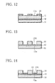
- FIG. 8 An example B 0 of the basic structure for the substrate according to the invention is shown in FIG. 8.
- the substrate B 0 is a plate-like piece having a sandwich structure comprising two Si layers 11,11 and an Si oxide layer 12 provided between them, where holes 13A reaching the surface 12a of the Si oxide layer 12 are formed in one of the Si layers 11 in a predetermined array pattern to function as bottomed wells.
- the surface 12a of the Si oxide layer 12 is exposed only at the bottoms of the holes 13A, and the other surface of the substrate B 0 is in Si. Only the surface of the Si oxide layer 12 functions as a reaction region for synthesizing, for example single-chain DNA, while all the other surface of the substrate B 0 functions as a non-reaction region.
- FIG. 9 shows another example B 1 of a substrate, which is made using the above-described substrate B 0 .
- a silane layer 14 is formed only at the bottoms of the holes 13A in the substrate B 0 .
- a spacer layer 15 of oligonucleotides (5T) each formed by synthesizing 5 units of DNA phophoramidite T successively.
- the holes 13A function as bottomed wells 13.
- the oligonucleotide (5T) spacer layer 15 which enables synthesis of probe DNA is exposed only at the bottoms 15a of the bottomed wells 13, while the side surfaces 15b of the bottomed wells 13 and the surface 11a of the Si layer 11 remain in Si.
- the bottoms of the bottomed wells 13 function as a reaction region for synthesizing probe DNA, while the other part including the side surfaces of the bottomed wells 13 and the substrate surface is a non-reaction region in the chemical synthesis of probe DNA, as it is, namely without undergoing surface inactivation treatment such as capping.
- the silane layer 14 in the substrate B 1 is provided so that the oligonucleotide (5T) spacer layer 15 can be synthesized efficiently, and is not indispensable, because the oligonucleotide (5T) spacer layer 15 can be synthesized directly on the surface 12a of the Si oxide layer 12.
- the substrate B 1 can be made as follows:
- a plate-like piece of a structure in which an Si oxide layer 12 is sandwiched between two Si layers 11, 11 is prepared. It is to be noted that one of the Si layers 11 should have a thickness almost equal to the depth of to-be-formed bottomed wells.
- an SOI (Silicon on Insulator) wafer commercially available from Shin-Etsu Chemical Co., Ltd. is suitable.
- the entire surface 11a of one of the Si layers 11 is covered with a resist 16, a mask having openings of the same diameter as that of the to-be-formed bottomed wells is placed on the resist, and ultraviolet rays are applied. Then, the mask is removed and the whole is developed.
- openings of the same diameter as that of the to-be-formed bottomed wells are formed in the resist 16, and the surface 11a of the Si layer 11 is exposed in these openings.
- etching is performed on the Si layer 11 using an Si etchant to form holes 13A reaching the surface 12a of the Si oxide layer 12.
- the etching automatically stops at the time the removal of the Si layer reaches the surface 12a of the Si oxide layer 12.
- the piece in which the surface 12a of the Si oxide layer 12 is exposed only at the bottoms of the holes 13A and the other surface part is made of Si is obtained. It is to be noted that the holes 13A in this piece have almost the same diameter and depth as those of the to-be-formed bottomed wells.
- silanization treatment is performed.
- the silanization reaction proceeds on the surface of the Si oxide layer, so that a silane layer 14 is formed only at the bottoms 12a of the holes 13A (FIG. 14).
- the silane layer 14 is made to react with DNA phosphoramidite T to form a spacer layer 15 of olygonucleotides (5T) each being a strand of sing-chain DNA of 5 mer T.
- 5T olygonucleotides
- DNA phophoramidite forms covalent bonding only with OH-group in the silance layer.
- the synthesis reaction proceeds only at the bottoms 12a of the bottomed wells.
- DNA phophoramidite T does not react with the part where Si is exposed, this part remains a non-reaction region although capping is not performed, unlike the case with the substrate A.
- step a 2 it is necessary to perform thermal oxidation treatment on the surface of the Si wafer to form an Si oxide layer. Meanwhile, the substrate B 1 (B 0 ) according to the invention does not require step a 2 .
- step a 5 a series of operations, namely filling the bottomed wells with resin droplets, capping, and dissolution and removal of the resin are indispensable. Meanwhile, the substrate B 1 according to the invention does not require these operations at all.
- the problems caused by supplying the bottomed wells with too much or too less an amount of resin droplets are obviated, and the boundary between the reaction region and the non-reaction region is definite.
- the reaction region consists only of the bottoms of the holes 13A formed by applying photolithography and etching, and the other surface part forms the non-reaction region.
- the substrate A in order to form the bottomed wells to have a depth according to design criteria, it is necessary to accurately manage etching time for etching in step a 1 .
- etching which removes parts of the Si layer 11 automatically stops at the time the removal reaches the surface of the Si oxide layer.
- the depth of the holes formed is determined uniquely by the thickness of the Si layer 11 used. Hence, the bottomed wells formed have a very accurate depth.
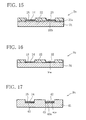
- FIG. 15 Another example B 2 of a substrate is shown in FIG. 15.
- Si oxide layer 21a In the substrate B 2 , on one side of an Si plate 21, only a superficial part is turned into an Si oxide layer 21a, for example by thermal oxidation. On this Si oxide layer 21a is formed a layer 22 of a material which does not react with biological substances such as DNA phosphoramidite T and is not corroded by organic solvents, acid solutions, alkali solutions or the like used in synthesis of DNA, in a predetermined thickness. Across the thickness of this layer 22, holes 23 of a predetermined diameter are formed up to the surface 21b of the Si oxide layer 21a, in a predetermined array pattern.
- the surface of the oligonucleotide (5T) spacer layer 15 capable of reacting with DNA phophoramidite T is exposed only at the bottoms of the holes 23 to form a reaction region. All the other surface part is a non-reaction region made of a material not reacting with DNA phophoramidite T, although it does not undergo inactivation treatment.
- the layer 22 which forms a non-reaction region
- metals not easily forming an oxide such as platinum, nitrides such as silicon nitride, plastics not having a reactive functional group such as polyethylene and polystyrene
- the layer 22 can be formed by a film formation method such as direct joint of the material as mentioned above to the Si oxide layer, vacuum deposition or CVD of the material as mentioned above onto the Si oxide layer surface, vapor phase polymerization of a monomer.
- the holes 23 can be formed by application of photolithography and etching, for example.
- FIG. 16 Another example B 3 of a substrate is shown in FIG. 16.
- the same layer 22 as that of the substrate B 2 is formed on a surface of a glass plate 31.
- holes 32 reaching the surface 31 a of the glass plate 31 are formed as bottomed wells, and only on the surface 31 a of the glass plate exposed at the bottoms of the holes 32, a silane layer 14 and an oligonucleotide (5T) spacer layer 15 are formed.
- the surface of the oligonucleotide (5T) spacer layer is exposed only at the bottoms 31 a of the holes 32 to form a reaction region.
- the side surfaces of the bottomed wells and the surface of the layer 22 form a non-reaction region although they do not undergo inactivation treatment.
- FIG. 17 Another example B 4 of a substrate is shown in FIG. 17.
- holes 42 of a predetermined diameter and depth are formed in a surface 41 a of a plate-like piece 41 made of a similar kind of material which does not react with DNA phosphoramidite T and is not corroded by organic solvents, acid solutions, alkali solutions or the like used in synthesis of DNA.
- These holes 42 are made into bottomed wells by forming an Si oxide layer 43 at the bottoms of the holes, and then forming a silane layer 14 and an oligonucleotide (5T) spacer on the Si oxide layer 43 in this order.
- the oligonucleotide (5T) spacer layer 15 located at the bottoms of the bottomed wells is only the part that can react with DNA phosphoramidite T, while the other part is a non-reaction region.
- Si and nitrides such as silicon nitride can be mentioned, for example.
- the above-mentioned bottomed wells can be formed by applying dry etching such as reactive ion etching or ion milling, or wet etching, for example.
- the bottomed wells may be formed as follows: By applying the SIMOX (Separation by Implanted Oxygen) method to put in oxygen ions from a surface of the Si plate, an Si oxide layer is formed at a certain depth from the surface of the Si plate. Then, by forming holes from the surface of the Si plate up to the Si oxide layer, the bottomed wells are obtained.
- SIMOX Separatation by Implanted Oxygen
- the bottomed wells may be formed as follows: A surface of the Si plate is once oxidized. Then by applying photolithography and etching to the resulting Si oxide surface layer, openings are formed in a predetermined array pattern. Then, oxygen ions are put in from the surface of Si exposed in the openings by the above-mentioned SIMOX method, and then the Si oxide surface layer is removed by etching. As a result, the structure in which an Si oxide layer extending only just under the places that were the openings is formed at a certain depth from the surface of the Si plate is obtained. Then, by forming holes from the surface of the Si plate up to the Si oxide layer in the places that were the openings, the bottomed wells are obtained.
- the substrate B 1 is prepared. As shown in a simplified manner in FIG. 18, in each of the bottomed wells 13 that are arranged in an array in the substrate B 1 , oligonucleotides (T5) space layer 15 having their terminals blocked with DMT are fixed only at the bottom of the bottomed well.
- T5 oligonucleotides
- Step b 1 Resin masking is performed for the bottomed wells. Specifically, of the bottomed wells arranged, all the bottomed wells except for those which should undergo chemical reaction with DNA phosphoramidite C (cytosine), for example are filled with resin droplets 6.
- DNA phosphoramidite C cytosine
- the oligonucleotides (5T) space layer in the bottomed well filled with resin droplet 6 are blocked by the resin, while the oligonucleotides (5T) space layer in the bottomed well not filled with resin droplet 6 are in a state that DMT at their terminals can be eliminated.
- Step b 2 Detritilation is performed by supplying a solution of an acid such as trichloroacetic acid evenly to the entire upper surface of the substrate.
- DMT is eliminated from the oligonucleotides (5T) space layer, so that those oligonucleotides (5T) space layer are activated.
- Step b 3 By supplying an organic solvent to the substrate surface, the resin droplet filling the bottomed wells is dissolved and removed.
- the activated oligonucleotides (5T) space layer and the oligonucleotides (5T) space layer having their terminals blocked with DMT are exposed.
- Step b 4 DNA coupling is performed by supplying a reagent containing DNA phosphoramidites C with their terminals blocked with DMT evenly to the entire surface of the substrate.
- synthesis reaction between the activated oligonucleotides (5T) space layer and the supplied DNA phosphoramidites C proceed, so that they are chemically combined together.
- the oligonucleotides grow by 1 mer, and the terminals of the grown oligonucleotides are blocked with DMT.
- the exposed oligonucleotides (5T) space layer have their terminals blocked with DMT and therefore are inactive. Hence, they do not react with the supplied DNA phosphoramidites C.
- probe DNA having sequences according to a design can be fixed only at the bottoms of the bottomed wells in the substrate B 1 .
- step b 1 DNA synthesis reaction proceeds only at the bottoms of the bottomed wells. The other part is not involved in the synthesis reaction at all. Hence, for example even if in step b 1 , resin droplet to fill a bottomed well runs over the bottomed well, it does not affect the DNA synthesis reaction at all unless the resin flows into adjacent bottomed wells, and therefore has no adverse effects on reading of fluorescent marks at all. Further, inactivation treatment (capping) which is performed in the case of the substrate A does not need to be performed any longer.
- all the substrates B 1 , B 2 , B 3 and B 4 are substrates for DNA chips in which the formation of the silane layer on the surface of the Si oxide layer of the substrate B 0 enables probe DNA synthesis reaction.
- substrates for biochips according to the present invention is not limited to this type.
- a material for forming the bottoms of the bottomed wells (reaction region) a material capable of fixing biological substances that bond to to-be-examined biological substances in a specific manner, different types of chips can be made.
- the part to which the linker substance is fixed can function as a reaction region specialized for reaction with that biological substance.
- the other part of the substrate forms a non-reaction region for that biological substance, and both regions are separated by a definite boundary.
- a silane coupling agent such as aminopropylemethoxysilane, or a substance having a functional group such as an epoxy group, a tosyl group, an activated carboxyl group, an amino group, a thiol group or a bromoatoamido group
- a biological substance having an amino group, a thiol group, a hydroxyl group, carboxyl group, a bromoatomamido group or the like at its terminal can be fixed on the surface of the Si oxide layer of the substrate B 0 by using the linker substance.
- double-chain DNA, proteins, peptides, sugars, RNA-protein complexes, or sugar-protain complexes as the biological substances, chips for detecting transcription factors that identify a specific base sequence of double-chain DNA and bond to it, a chip for detecting peptides, a chip for detecting proteins, a chip for detecting sugars, a chip for digesting proteins or the like can be made.
- a substrate B 1 having a final structure shown in FIG. 9 was made by the process shown in FIGS. 10 to 14.
- the specifications of the substrate B 1 were as follows:
- the silane layer was formed using 5,6-epoxytriethoxysilane, and the oligonucleotide spacer layer was formed by the phosphoramidite method using a DNA synthesizing reagent produced by Proligo Japan K.K.
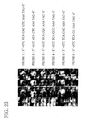
- FIG. 23 is a photograph showing the results.
- spots corresponding to probe 4 were highest in fluorescence intensity. From this, it turned out that the sequence of the target DNA was 5'-TAGAGTGGGTTTATC-3'.
- a substrate A having a structure shown in FIG. 7 was made by performing capping according to the method disclosed in PCT Application Published Japanese Translation No. 2002-537869.
- Target DNA detection test was performed in the same manner as in the Example.
- FIG. 24 shows the results.
- each spot corresponding to probe 4 a central part of each spot was weak in fluorescent color. This comes from the fact that too less an amount of resin droplets was supplied to fill the wells. Meanwhile, each spot as a whole was high in fluorescence intensity. This is because the probe DNA fixed in these spots was complementary to the target DNA.
- the boundary between the fluorescent-colored spots and the substrate surface was very clear and background noise was virtually not produced.
- each fluorescent-colored spot showed an even fluorescence intensity, and measured data was stable.
- the boundary between the reaction region for synthesizing biological substances and the non-reaction region is quite definite.
- a biochip made using this substrate makes it possible to detect to-be-detected biological substances stably and with high accuracy.
- sites forming the reaction region are formed by photolithography and etching in the process of making the substrate. This increases the freedom of formation and enables fine patterns and therefore high-density formation of the reaction region. Further, since the making process does not need to include the steps of filling the bottomed wells with resin droplets and then performing inactivation treatment, the overall production costs decrease.
- this substrate for biochips has a large industrial value.
Priority Applications (10)
| Application Number | Priority Date | Filing Date | Title |
|---|---|---|---|
| EP04291742A EP1614460A1 (fr) | 2004-07-08 | 2004-07-08 | Substrat pour biopuces |
| CN2004800435402A CN101001692B (zh) | 2004-07-08 | 2004-12-16 | 生物芯片基底和制造生物芯片基底的方法 |
| PCT/JP2004/019285 WO2006006262A1 (fr) | 2004-07-08 | 2004-12-16 | Substrat pour biopuce et procede de fabrication de substrat pour biopuce |
| CN201010220809.7A CN101884899B (zh) | 2004-07-08 | 2004-12-16 | 生物芯片基底和制造生物芯片基底的方法 |
| CN201010220792.5A CN101884898B (zh) | 2004-07-08 | 2004-12-16 | 生物芯片基底和制造生物芯片基底的方法 |
| US11/631,646 US7807105B2 (en) | 2004-07-08 | 2004-12-16 | Substrate for biochip |
| JP2005194381A JP4710031B2 (ja) | 2004-07-08 | 2005-07-01 | バイオチップ用基板 |
| US12/844,863 US8287939B2 (en) | 2004-07-08 | 2010-07-28 | Method for manufacturing substrate for biochip |
| JP2011006343A JP5373828B2 (ja) | 2004-07-08 | 2011-01-14 | バイオチップ用基板 |
| JP2011006344A JP5372033B2 (ja) | 2004-07-08 | 2011-01-14 | バイオチップ用基板の製造方法 |
Applications Claiming Priority (1)
| Application Number | Priority Date | Filing Date | Title |
|---|---|---|---|
| EP04291742A EP1614460A1 (fr) | 2004-07-08 | 2004-07-08 | Substrat pour biopuces |
Publications (1)
| Publication Number | Publication Date |
|---|---|
| EP1614460A1 true EP1614460A1 (fr) | 2006-01-11 |
Family
ID=34931234
Family Applications (1)
| Application Number | Title | Priority Date | Filing Date |
|---|---|---|---|
| EP04291742A Withdrawn EP1614460A1 (fr) | 2004-07-08 | 2004-07-08 | Substrat pour biopuces |
Country Status (4)
| Country | Link |
|---|---|
| US (2) | US7807105B2 (fr) |
| EP (1) | EP1614460A1 (fr) |
| CN (3) | CN101001692B (fr) |
| WO (1) | WO2006006262A1 (fr) |
Cited By (3)
| Publication number | Priority date | Publication date | Assignee | Title |
|---|---|---|---|---|
| WO2008034871A1 (fr) * | 2006-09-22 | 2008-03-27 | Commissariat A L'energie Atomique | Composants fluidiques double-face |
| EP1939621A1 (fr) * | 2005-09-16 | 2008-07-02 | Yamatake Corporation | Substrat pour biopuce, biopuce, procédé de fabrication d 'un substrat pour biopuce et procédé de fabrication d 'une biopuce |
| US20120108787A1 (en) * | 2009-02-26 | 2012-05-03 | Nubiome, Inc. | Immobilization Particles for Removal of Microorganisms and/or Chemicals |
Families Citing this family (14)
| Publication number | Priority date | Publication date | Assignee | Title |
|---|---|---|---|---|
| TW200837349A (en) * | 2007-03-07 | 2008-09-16 | Nat Univ Tsing Hua | Biochip and manufacturing method thereof |
| JP4850855B2 (ja) * | 2007-03-22 | 2012-01-11 | 信越化学工業株式会社 | マイクロアレイ作製用基板の製造方法 |
| JP5485772B2 (ja) * | 2010-03-31 | 2014-05-07 | 株式会社エンプラス | マイクロ流路チップ及びマイクロ分析システム |
| CN106198656B (zh) | 2010-08-18 | 2018-12-11 | 生命科技股份有限公司 | 用于电化学检测装置的微孔的化学涂层 |
| JP2013088378A (ja) * | 2011-10-21 | 2013-05-13 | Sony Corp | ケミカルセンサ、ケミカルセンサモジュール、生体分子検出装置及び生体分子検出方法 |
| WO2013138767A1 (fr) * | 2012-03-16 | 2013-09-19 | Life Technologies Corporation | Systèmes et procédés d'analyse biologique |
| US9063072B1 (en) | 2012-06-12 | 2015-06-23 | Maven Technologies, Llc | Birefringence correction for imaging ellipsometric bioassay system and method |
| KR102592368B1 (ko) * | 2014-07-02 | 2023-10-25 | 라이프 테크놀로지스 코포레이션 | 반도체 센서의 표면 처리 |
| CN106536710B (zh) * | 2014-08-08 | 2018-07-06 | 应用材料公司 | 用于生物医用器件的液膜的图案化沉积 |
| CN104569383A (zh) * | 2015-01-13 | 2015-04-29 | 科蒂亚(新乡)生物技术有限公司 | 一种在聚乙烯微孔板上包被核酸的方法 |
| CN107049587A (zh) * | 2017-05-14 | 2017-08-18 | 郭宝煊 | 智能月经杯 |
| CN111013679A (zh) * | 2019-12-27 | 2020-04-17 | 江苏集萃微纳自动化系统与装备技术研究所有限公司 | 一种纸基微流控芯片的制备方法及纸基微流控芯片 |
| CN111606574A (zh) * | 2020-06-11 | 2020-09-01 | 江南大学 | 糖基超亲水改性的防雾玻璃及其制备方法与应用 |
| CN113607714B (zh) * | 2021-10-08 | 2022-01-11 | 成都齐碳科技有限公司 | 分子膜成膜或表征器件、装置、方法以及生物芯片 |
Citations (5)
| Publication number | Priority date | Publication date | Assignee | Title |
|---|---|---|---|---|
| WO1998059243A1 (fr) * | 1997-06-24 | 1998-12-30 | The Trustees Of Boston University | Support pour streptavidine haute densite |
| JPH1164213A (ja) * | 1997-06-09 | 1999-03-05 | Fuji Photo Film Co Ltd | サンプルプレート |
| WO1999039829A1 (fr) * | 1998-02-04 | 1999-08-12 | Merck & Co., Inc. | Puits virtuels destines a etre utilises dans des criblages a haut rendement |
| FR2787581A1 (fr) * | 1998-12-16 | 2000-06-23 | Commissariat Energie Atomique | Procede et equipement de garnissage de sites d'une biopuce |
| EP1245278A2 (fr) * | 2000-09-15 | 2002-10-02 | Agfa-Gevaert | Matériau en bande ayant descmicropuits pour des applications dans la chimie combinatoire |
Family Cites Families (17)
| Publication number | Priority date | Publication date | Assignee | Title |
|---|---|---|---|---|
| US5474796A (en) | 1991-09-04 | 1995-12-12 | Protogene Laboratories, Inc. | Method and apparatus for conducting an array of chemical reactions on a support surface |
| DE69324716T2 (de) * | 1992-02-13 | 1999-09-09 | Becton Dickinson Co | Celithydrat und Reinigung von DNS |
| KR100314996B1 (ko) | 1994-11-10 | 2002-01-15 | 윌리암 제이. 버크 | 액체분배시스템 |
| JP4313861B2 (ja) * | 1997-08-01 | 2009-08-12 | キヤノン株式会社 | プローブアレイの製造方法 |
| FR2790766B1 (fr) | 1999-03-08 | 2002-12-20 | Commissariat Energie Atomique | Procede de realisation d'une matrice de sequences de molecules chimiques ou biologiques pour dispositif d'analyse chimique ou biologique |
| US6752966B1 (en) | 1999-09-10 | 2004-06-22 | Caliper Life Sciences, Inc. | Microfabrication methods and devices |
| AU1476601A (en) * | 1999-11-09 | 2001-06-06 | Sri International | Array for the high-throughput synthesis, screening and characterization of combinatorial libraries, and methods for making the array |
| AU2001269477A1 (en) * | 2000-07-06 | 2002-01-21 | Asahi Kasei Kabushiki Kaisha | Molecule detecting sensor |
| DE60125598T2 (de) * | 2001-06-08 | 2007-10-04 | Centre National De La Recherche Scientifique | Methode zur herstellung einer mikroflüssigkeitsstruktur, insbesondere eines "biochips", und damit erzeugte struktur |
| WO2003014722A1 (fr) * | 2001-08-08 | 2003-02-20 | The Arizona Board Of Regents | Transistor a effet de champ a acide nucleique |
| US7097882B2 (en) | 2001-08-21 | 2006-08-29 | Samsung Sdi Co., Ltd. | Substrate for immobilizing physiological material, and method of fabricating same |
| WO2003046508A2 (fr) * | 2001-11-09 | 2003-06-05 | Biomicroarrays, Inc. | Substrats a surface importante pour micro-reseaux et procedes de fabrication |
| JP4121762B2 (ja) | 2002-03-28 | 2008-07-23 | オリンパス株式会社 | 蛍光検出用支持体 |
| CN1184332C (zh) * | 2002-04-24 | 2005-01-12 | 公准精密工业股份有限公司 | 阵列式生物芯片 |
| DE10221799A1 (de) * | 2002-05-15 | 2003-11-27 | Fujitsu Ltd | Silicon-on-Insulator-Biosensor |
| FR2844725B1 (fr) | 2002-09-24 | 2005-01-07 | Commissariat Energie Atomique | Procede de fabrication d'une membrane biomimetique, membrane biomimetique et ses applications |
| JP2006507504A (ja) | 2002-11-22 | 2006-03-02 | ソルス バイオシステムズ インコーポレーテッド | 並列振動分光法による高スループットのスクリーニング |
-
2004
- 2004-07-08 EP EP04291742A patent/EP1614460A1/fr not_active Withdrawn
- 2004-12-16 CN CN2004800435402A patent/CN101001692B/zh not_active Expired - Fee Related
- 2004-12-16 CN CN201010220792.5A patent/CN101884898B/zh not_active Expired - Fee Related
- 2004-12-16 US US11/631,646 patent/US7807105B2/en not_active Expired - Fee Related
- 2004-12-16 CN CN201010220809.7A patent/CN101884899B/zh not_active Expired - Fee Related
- 2004-12-16 WO PCT/JP2004/019285 patent/WO2006006262A1/fr active Application Filing
-
2010
- 2010-07-28 US US12/844,863 patent/US8287939B2/en not_active Expired - Fee Related
Patent Citations (5)
| Publication number | Priority date | Publication date | Assignee | Title |
|---|---|---|---|---|
| JPH1164213A (ja) * | 1997-06-09 | 1999-03-05 | Fuji Photo Film Co Ltd | サンプルプレート |
| WO1998059243A1 (fr) * | 1997-06-24 | 1998-12-30 | The Trustees Of Boston University | Support pour streptavidine haute densite |
| WO1999039829A1 (fr) * | 1998-02-04 | 1999-08-12 | Merck & Co., Inc. | Puits virtuels destines a etre utilises dans des criblages a haut rendement |
| FR2787581A1 (fr) * | 1998-12-16 | 2000-06-23 | Commissariat Energie Atomique | Procede et equipement de garnissage de sites d'une biopuce |
| EP1245278A2 (fr) * | 2000-09-15 | 2002-10-02 | Agfa-Gevaert | Matériau en bande ayant descmicropuits pour des applications dans la chimie combinatoire |
Non-Patent Citations (1)
| Title |
|---|
| PATENT ABSTRACTS OF JAPAN vol. 1999, no. 08 30 June 1999 (1999-06-30) * |
Cited By (8)
| Publication number | Priority date | Publication date | Assignee | Title |
|---|---|---|---|---|
| EP1939621A1 (fr) * | 2005-09-16 | 2008-07-02 | Yamatake Corporation | Substrat pour biopuce, biopuce, procédé de fabrication d 'un substrat pour biopuce et procédé de fabrication d 'une biopuce |
| EP1939621A4 (fr) * | 2005-09-16 | 2009-05-13 | Yamatake Corp | Substrat pour biopuce, biopuce, procédé de fabrication d 'un substrat pour biopuce et procédé de fabrication d 'une biopuce |
| US8198071B2 (en) | 2005-09-16 | 2012-06-12 | Azbil Corporation | Substrate for biochip, biochip, method for manufacturing substrate for biochip, and method for manufacturing biochip |
| WO2008034871A1 (fr) * | 2006-09-22 | 2008-03-27 | Commissariat A L'energie Atomique | Composants fluidiques double-face |
| FR2906237A1 (fr) * | 2006-09-22 | 2008-03-28 | Commissariat Energie Atomique | Composants fluidiques double-face |
| US20120108787A1 (en) * | 2009-02-26 | 2012-05-03 | Nubiome, Inc. | Immobilization Particles for Removal of Microorganisms and/or Chemicals |
| US10245279B2 (en) | 2009-02-26 | 2019-04-02 | Nubiome, Inc. | Use of immobilization particles for removal of microorganisms and/or chemicals |
| US11083746B2 (en) | 2009-02-26 | 2021-08-10 | Nubiome, Inc. | Use of immobilization particles for removal of microorganisms and/or chemicals |
Also Published As
| Publication number | Publication date |
|---|---|
| CN101884898A (zh) | 2010-11-17 |
| WO2006006262A1 (fr) | 2006-01-19 |
| US20080253928A1 (en) | 2008-10-16 |
| US8287939B2 (en) | 2012-10-16 |
| US7807105B2 (en) | 2010-10-05 |
| CN101884898B (zh) | 2013-05-01 |
| CN101001692A (zh) | 2007-07-18 |
| CN101001692B (zh) | 2011-05-11 |
| US20100288727A1 (en) | 2010-11-18 |
| CN101884899B (zh) | 2013-04-03 |
| CN101884899A (zh) | 2010-11-17 |
Similar Documents
| Publication | Publication Date | Title |
|---|---|---|
| US8287939B2 (en) | Method for manufacturing substrate for biochip | |
| EP0969083B1 (fr) | Capillaire d'adn | |
| JP4562914B2 (ja) | 化学的または生物学的分析マルチポイントマイクロシステム | |
| JP4710031B2 (ja) | バイオチップ用基板 | |
| US6881379B1 (en) | Method for producing detection systems with planar arrays | |
| US11747263B2 (en) | Flow cells and methods related to same | |
| JP3872227B2 (ja) | 新規の生物学的チップ及び分析方法 | |
| US6559296B2 (en) | DNA capillary | |
| KR20030014162A (ko) | 생체분자 마이크로어레이의 제조방법 및 장치 | |
| JP2003516748A (ja) | バイオアレイ作成用の装置および方法 | |
| JP2003232791A (ja) | プローブ固相化反応アレイ | |
| JP4262512B2 (ja) | プローブ固相化反応アレイ | |
| US7341865B1 (en) | Liquid delivery devices and methods | |
| JP5373828B2 (ja) | バイオチップ用基板 | |
| JP5372033B2 (ja) | バイオチップ用基板の製造方法 | |
| JP4167431B2 (ja) | 生化学的検査用の検査基板 | |
| TWI831827B (zh) | 流體槽及與其相關之方法 | |
| JP2004195730A (ja) | 樹脂成形品の製造方法及び金型の製造方法、並びに樹脂成形品及びチップ | |
| JP2002286707A (ja) | プローブ担体およびその製造方法 |
Legal Events
| Date | Code | Title | Description |
|---|---|---|---|
| PUAI | Public reference made under article 153(3) epc to a published international application that has entered the european phase |
Free format text: ORIGINAL CODE: 0009012 |
|
| AK | Designated contracting states |
Kind code of ref document: A1 Designated state(s): AT BE BG CH CY CZ DE DK EE ES FI FR GB GR HU IE IT LI LU MC NL PL PT RO SE SI SK TR |
|
| AX | Request for extension of the european patent |
Extension state: AL HR LT LV MK |
|
| AKX | Designation fees paid | ||
| REG | Reference to a national code |
Ref country code: DE Ref legal event code: 8566 |
|
| STAA | Information on the status of an ep patent application or granted ep patent |
Free format text: STATUS: THE APPLICATION IS DEEMED TO BE WITHDRAWN |
|
| 18D | Application deemed to be withdrawn |
Effective date: 20060712 |