EP1608071A1 - Reconfigurable logical circuit using transistor having spin-dependent transmission characteristic - Google Patents
Reconfigurable logical circuit using transistor having spin-dependent transmission characteristic Download PDFInfo
- Publication number
- EP1608071A1 EP1608071A1 EP04723782A EP04723782A EP1608071A1 EP 1608071 A1 EP1608071 A1 EP 1608071A1 EP 04723782 A EP04723782 A EP 04723782A EP 04723782 A EP04723782 A EP 04723782A EP 1608071 A1 EP1608071 A1 EP 1608071A1
- Authority
- EP
- European Patent Office
- Prior art keywords
- circuit
- mosfet
- spin
- terminal
- channel
- Prior art date
- Legal status (The legal status is an assumption and is not a legal conclusion. Google has not performed a legal analysis and makes no representation as to the accuracy of the status listed.)
- Withdrawn
Links
Images


















Classifications
-
- H—ELECTRICITY
- H03—ELECTRONIC CIRCUITRY
- H03K—PULSE TECHNIQUE
- H03K19/00—Logic circuits, i.e. having at least two inputs acting on one output; Inverting circuits
- H03K19/20—Logic circuits, i.e. having at least two inputs acting on one output; Inverting circuits characterised by logic function, e.g. AND, OR, NOR, NOT circuits
-
- H—ELECTRICITY
- H03—ELECTRONIC CIRCUITRY
- H03K—PULSE TECHNIQUE
- H03K19/00—Logic circuits, i.e. having at least two inputs acting on one output; Inverting circuits
- H03K19/02—Logic circuits, i.e. having at least two inputs acting on one output; Inverting circuits using specified components
- H03K19/08—Logic circuits, i.e. having at least two inputs acting on one output; Inverting circuits using specified components using semiconductor devices
- H03K19/094—Logic circuits, i.e. having at least two inputs acting on one output; Inverting circuits using specified components using semiconductor devices using field-effect transistors
- H03K19/0944—Logic circuits, i.e. having at least two inputs acting on one output; Inverting circuits using specified components using semiconductor devices using field-effect transistors using MOSFET or insulated gate field-effect transistors, i.e. IGFET
-
- H—ELECTRICITY
- H10—SEMICONDUCTOR DEVICES; ELECTRIC SOLID-STATE DEVICES NOT OTHERWISE PROVIDED FOR
- H10D—INORGANIC ELECTRIC SEMICONDUCTOR DEVICES
- H10D48/00—Individual devices not covered by groups H10D1/00 - H10D44/00
- H10D48/385—Devices using spin-polarised carriers
Definitions
- the present invention relates to logic circuits with reconfigurable functions, and more particularly, to a reconfigurable logic circuit using transistors (hereafter referred to as the "spin transistors") that contain ferromagnetic bodies and have transfer characteristics depending on the magnetization states of the ferromagnetic bodies.
- spin transistors transistors
- FPGA field programmable logic array
- the FPGA is incorporated as the last component into mobile devices such as portable telephone devices that tend to be replaced with newly developed devices in a short time. Also, studies have been made on the FPGA as an information device of novel architecture that reconfigures its hardware for each operation.
- LUT Look Up Table
- a desired logic circuit is realized by rewriting the values to be written in the register of the LUT and the switch for the lines.
- Each logic block includes a flip-flop (FF) for operations in synchronization with the LUT (see Fig. 56B).
- the LUT includes a decoder circuit for matching each input pattern with an address, and memories (SRAM cells) for storing a value in the register of each address.
- Fig. 56C shows an example of the LUT circuit that can achieve symmetric Boolean functions.
- a SRAM is a volatile memory, and loses stored information when the power supply is cut off. Therefore, so as to maintain data, a non-volatile memory (a flash memory, for example) is prepared externally, and the information stored in the non-volatile memory is loaded every time the power supply is resumed.
- a non-volatile memory a flash memory, for example
- Fig. 56 illustrates an example structure of a logic circuit that can achieve symmetric Boolean functions.
- This logic circuit includes three pre-inverters 201, 203, and 205 that employ ⁇ MOS structures, and a main inverter 207 that also employs the ⁇ MOS structure.
- the pre-inverters that serve as input units digital values are input via equal capacitances.
- the inverters 201, 203, 205, and 207 have different logic threshold values from one another.
- V k /n indicates that the number of inputs to the inverter is n
- the logic threshold value is V k /n with respect to the logic level "1".
- the above described logic blocks of the FPGA have the following problems. More specifically, the logic blocks that utilizes the LUT method and ⁇ MOS have problems in the volatility of logic functions. Also, problems are caused with respect to the number of devices (the occupied area).
- the problems with the logic blocks according to the LUT method are described.
- the circuit does not have capacity to rewrite to reconfigure logics, but refers to the values stored in the registers.
- SRAMs are employed for LUTs, the problems are caused by the volatility of the SRAMs.
- the power supply is cut off, the contents of the LUTs, or the logic functions, are lost.
- the circuit is incorporated into a product, it is necessary to externally provide a non-volatile memory with an extremely large capacity for maintaining data. As a result, the area of the entire chip becomes larger, and the power consumption increases as a longer start-up time is required when power supply is resumed.
- a transistor (hereinafter referred to as "spin transistor") with transfer characteristics that depend on the spin direction of the conduction carriers or the magnetization states of the ferromagnetic bodies in the transistor is employed, and the input of the transistor is formed with a ⁇ MOS transistor.
- the operating point of the circuit is adjusted to rewrite functions by varying the driving force of the transistor through the control of the magnetization state of the spin transistor.
- This circuit is based on a novel technique of rewriting functions entirely in terns of hardware, as the characteristics of the device are changed.
- This circuit differs from a logic block only with a ⁇ MOS in that logic functions can be maintained in a non-volatile manner and a control signal is not required for switching logic functions.
- the functions of the circuit can be stored in a non-volatile manner, by virtue of the ferromagnetic bodies in the spin transistor. Using such a logic circuit of the present invention, the above described problems in FPGA can be eliminated.
- the non-volatility is now described.
- the functions of a circuit are determined by the magnetization states of the ferromagnetic bodies included in the spin transistor. Accordingly, even when the power supply is cut off, the logic functions are maintained in a non-volatile manner, as the magnetization states do not change. In view of this, the portion corresponding to a logic block unit that is necessary in the conventional FPGA becomes unnecessary in an external non-volatile memory. This is advantageous in reducing the chip size. Furthermore, the time for loading logic functions is not required. Accordingly, the time required for start-up can also be shortened.
- the logic block includes nine to eleven MOSFETs and two capacitors. Accordingly, the number of devices decreases to a third of the number of device in the LUT structure or even less than that. Compared with a logic block using only a ⁇ MOS, the number of devices is halved. Since the external non-volatile memories are employed only for the line unit, the total number of devices is much smaller than that in a conventional circuit.
- a spin transistor can be employed as a switch for selecting the line that connects logic blocks.
- a spin MOSFET that is described later is employed as the switch, so that the mutual lines between logic blocks can also be stored in a non-volatile manner. In such a case, a non-volatile memory becomes unnecessary for the line unit.
- the spin MOSFET as the switch may be a depletion MOSFET or an enhancement MOSFET. Further, a transfer gate that is formed with p-channel and n-channel spin MOSFETs can also be employed.
- One aspect of the present invention can provide a circuit that includes a spin transistor having transfer characteristics depending on the spin direction of conduction carriers.
- the spin direction of the conduction carriers is changed so as to vary the transfer characteristics of the spin transistor, and an operating point is changed based on the transfer characteristics, thereby reconfiguring a function.
- An A-D converter is connected to an output terminal of the circuit, so that the analog operating point at the output terminal is converted to a digital logic level. Also, the A-D converter includes a spin transistor, so that functions can be reconfigured by setting a threshold value depending on the magnetization state of the spin transistor.
- the spin transistor instead of the spin transistor, another spin transistor with variable transfer characteristics can be employed in the circuit.
- the operating point is also moved by changing the transfer characteristics of the transistor, thereby reconfiguring functions.
- the "variable transfer characteristics" are variable solid-state properties other than the biases such as V ds and V gs , and the transfer characteristics of a transistor can be varied in a non-volatile manner. Accordingly, the output characteristics vary, even when biases are applied under the same conditions.
- Such a transistor can be realized with a ferromagnetic material or a ferroelectric material, or can be formed by a floating gate technique (by which carriers are injected to a floating gate so as to change a threshold value).
- the above described spin transistor is one of the transistors with variable transfer characteristics.
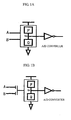
- the circuit in accordance with the present invention includes a terminal V m (hereinafter, "V m " will be used as the name of the terminal, but will also be used as the potential of the terminal), a circuit group P that charges the terminal V m with parasitic capacitance and the next stage with input capacitance, a circuit group Q for discharging, and an A-D converter that amplifies the analog voltage V m to a digital logic level.
- V m a terminal V m
- V m the terminal V m
- P that charges the terminal V m with parasitic capacitance and the next stage with input capacitance
- a circuit group Q for discharging
- an A-D converter that amplifies the analog voltage V m to a digital logic level.
- the voltage V m is determined by the values of input signals A and B, regardless of the circuit of the next stage.
- a spin transistor is contained in at least one of the circuit groups P and Q, and the current control capacity can be controlled in accordance with the magnetization state of the spin transistor. Therefore, even if the input signals A and B have the same values, the voltage V m varies depending on the magnetization state of the spin transistor.
- the variation of V m caused by a change in the magnetization sate of the spin transistor is amplified to the digital logic level by the A-D converter having a predetermined logic threshold value, thereby forming a reconfigurable logic circuit.
- a reconfigurable logic circuit can be formed.
- the circuit shown in Fig. 1B has a 2-input ⁇ -MOS structure with equally weighted inputs.
- the input signals A and B do not need to be distinguished from each other. Accordingly, with the 2-input ⁇ -MOS structure having equally weighted inputs, inputs can be efficiently performed to the circuit groups. If there is a need to distinguish the input signals A and B from each other, the weights on the input capacity should be made different from each other between the input signals A and B.
- the circuit in accordance with the present invention contains ferromagnetic bodies made of a ferromagnetic metal or the like.
- This circuit is a non-volatile, reconfigurable circuit, and more particularly, is a logic circuit that employs a spin transistor that can control its transfer characteristics in accordance with the spin direction of the conduction carriers or the magnetization states of the ferromagnetic bodies. Using the spin transistor, a symmetric Boolean function can be realized with a small number of components.
- the spin transistor has at least one ferromagnetic body (free layer) with a magnetization direction that can be independently controlled with a magnetic field or the like, and at least one ferromagnetic body (pin layer) with a fixed magnetization direction.
- the relative magnetization state between the free layer and the pin layer can be switched between parallel magnetization and antiparallel magnetization by changing the magnetization direction of the free layer.
- the spin transistor output characteristics in accordance with the magnetization state inside can be realized by virtue of the conduction phenomena, such as spin-dependent scattering, a spin-dependent tunneling effect, and a spin filter effect, which depend on the spin direction of the carriers and the magnetization directions of the ferromagnetic bodies. Accordingly, the transfer characteristics of the spin transistor can be controlled in accordance with the relative magnetization direction of the pin layer with respect to the free layer contained in the spin transistor, even when the same biases are applied.
- spin MOSFET MOSFET spin transistor
- spin MOSFET MOSFET spin transistor
- the transistor operation is based on the same principles as those of the operation of a conventional MOSFET.
- the output characteristics can be represented by gradual channel approximation.
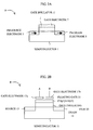
- Fig. 2A illustrates an example structure of a spin MOSFET.
- the spin MOSFET (A) is formed on a semiconductor (substrate) 1, and has the same structure as a conventional MOSFET, including the aspect that a gate electrode 7 is formed on a gate insulating film 11.
- the spin MOSFET (A) differs from a conventional MOSFET in that a source electrode 3 and a drain electrode 5 are made of a ferromagnetic material.
- the source electrode made of a ferromagnetic material will be referred to simply as the ferromagnetic source 3, and the drain electrode made of a ferromagnetic material will be referred to simply as the ferromagnetic drain 5.
- “FM” indicates “ferromagnetic metal”, but the source and drain may be made of some other electric conductive ferromagnetic material.
- the ferromagnetic source 3 serves as a spin injector that injects spin-polarized carriers to a channel formed below the gate in the semiconductor 1.
- the ferromagnetic drain 5 serves as a spin analyzer that detects an electric signal representing the direction of the spins injected to the channel.
- the ferromagnetic source 3 and the ferromagnetic drain 5 are formed with the Schottky junctions with the semiconductor (substrate) 1.
- a gate voltage is applied to the gate electrode 7, so that spin-polarized carriers can be injected from the ferromagnetic source 3 to the channel via a Schottky barrier.
- the injected spin-polarized carriers reach the ferromagnetic drain 5 via the channel (for ease of explanation, the Rashba effect caused by the gate field of the spin-polarized carriers injected to the channel is ignored).
- the spin-polarized carriers injected to the ferromagnetic drain 5 become a drain current, without adverse influence of spin-dependent scattering.
- the ferromagnetic drain 5 is subjected to the resistance due to spin-dependent scattering. Accordingly, in the spin MOSFET, the current drive force varies depending on the relative magnetization direction between the source and the drain.
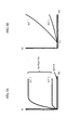
- Figs. 3A and 3B show idealized static characteristics of a spin MOSFET.
- a gate voltage equal to or lower than a threshold value (V gs ⁇ V th ) the spin MOSFET is in an OFF state, as in the case of a conventional MOS transistor. This does not change with the magnetization state of the spin MOSFET.
- V gs V gs1 ⁇ V th
- the spin MOSFET is put into an ON state.
- the drain current I d varies depending on the magnetization state of the ferromagnetic bodies included in the spin MOSFET.
- a high drain current I d ⁇ flows.
- a low drain current I d ⁇ flows.
- the drain current of the spin MOSFET can be represented using the same gain coefficient as that of a conventional MOSFET, the gain coefficient is high in the case of parallel magnetization, and the gain coefficient is low in the case of antiparallel magnetization.
- relative parameters ⁇ representing the gain coefficients of the spin MOSFETs and the MOSFETs are introduced. With the gain coefficients of the spin MOSFETs and the MOSFETs included in the circuit being ⁇ G1 , ⁇ G2 ...
- ⁇ G1 ⁇ 1 ⁇ G1
- ⁇ G2 ⁇ 2 ⁇ G1
- ⁇ G3 ⁇ 3 ⁇ G1
- ... ⁇ GN ⁇ N ⁇ G1 , using the gain coefficient ⁇ G1 .
- ⁇ N is expressed with given numerals, the numeric values ⁇ are merely examples of representations of the magnitude correlation, and those numeric values do not limit the scope of the present invention. Also, the magnitude correlation among the gain coefficients ⁇ 1 , ⁇ 2 , ... ⁇ N indicates an example of the magnitude correlation among output currents when the same bias is applied to the MOSFET and the spin MOSFET, including a case where the output characteristics of the spin MOSFET cannot be expressed with the output characteristics of the conventional MOSFET.
- a MOSFET (B) with a ⁇ MOS structure includes a source 13 and a drain 15 that are formed on a semiconductor 11, a floating gate 21 formed above the semiconductor 11 via a gate insulating film 20, and two divided gate electrodes 17a and 17b.
- inputs A and B are input to the gates 17a and 17b of the ⁇ MOS structure via the input capacitances of the gate electrode and the floating gate.
- the inputs can be weighted by varying the magnitudes of the gate electrode and the floating gate.
- a case where all the input capacitances are equal to one another is described as an example.
- n inputs n>2
- An AND/OR reconfigurable logic circuit can be realized using the inputs of the ⁇ MOS structure and an inverter structure having an E/E configuration, an E/D configuration, or a CMOS configuration formed with spin MOSFETS and conventional MOSFETS as the circuit structure of the circuit group P and the circuit group Q.
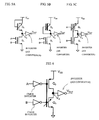
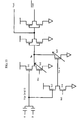
- Figs. 5A, 5B, and 5C illustrate AND/OR reconfigurable logic circuits using the inverter structures of the E/E configuration, the E/D configuration, and the CMOS configuration.
- each spin MOSFET will be indicated by a transistor symbol with an arrow.
- spin MOSFETs are used for active loads (Q2) of the inverters of the E/E configuration, the E/D configuration, and the CMOS configuration.
- spin MOSFETs may be used for drivers (Q1).
- both the active loads (Q2) and the drivers (Q1) may be formed with spin MOSFETs.
- the input ⁇ MOS structure is used for the drivers (Q1) in the E/E configuration and the E/D configuration.
- the ⁇ MOS structure is realized with a floating gate shared between Q2 and Q1.
- the inverter in the output stage is used to divide the output of V m into the logic levels of "1" and "0". This inverter serves as an A-D converter.
- the active load Q2 in each of Figs. 5A through 5C forms the circuit group P, while the driver Q1 forms the circuit group Q.
- an extra circuit for controlling the potential of V m in each of the circuits of Figs. 5A through 5C is added to the circuit group P and the circuit group Q, thereby achieving a complicated, reconfigurable logic circuit.
- the driver or the active load of an E/D inverter circuit formed with an enhancement MOSFET and a depletion MOSFET is replaced with a spin MOSFET.
- an enhancement spin MOSFET should be employed.
- a depletion spin MOSFET should be employed.
- the input ⁇ MOS structure is used for the driver.
- a CMOS inverter is most preferred in terms of performance, but it is possible to employ an inverter of another type, such as an E/D inverter.
- the load curve in the E/E configuration varies according to the voltage generated in the driver.
- the load curve with the active load is saturated. Accordingly, a wider logic margin can be allowed.
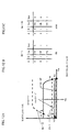
- Figs. 7 through 9 an AND/OR circuit with a n-channel spin MOSFET of a depletion type is described.
- Tr1 the n-channel spin MOSFET of a depletion type
- the parameter ⁇ n1 can be 1 or 10 in the case of antiparallel magnetization or parallel magnetization. Since the source and the gate of Tr1 are shortcircuited, the load curve is saturated with respect to Vm as indicated by the solid line in Fig. 8.
- a ⁇ MOS structure is used for the input of a transistor Tr2, and its operation can be as indicated by the broken line in Fig. 8.
- Figs. 9A and 9B are the truth tables of this circuit. Also, the details of the operation are shown in Table 1.
- the spin MOSFET is put into the antiparalell magnetization configuration, and the parameter ⁇ n1 is set at 1, with which the current driving capacity is small.
- the operating point V m is V 0 according to Fig. 8, and the output V out is inverted and amplified to "0".
- the operating point V m is V P , and accordingly, the output V out is "1".
- the spin MOSFET is put into the parallell magnetization configuration, and the parameter ⁇ n1 is set at 10, with which the current driving capacity is large.
- the operating point V m is V 0 , and accordingly, the output V out is "0".
- the operating point V m is V R , and accordingly, the output V out is "0".
- the operating point V m is V s , and accordingly, the output V out is "1".
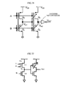
- Fig. 10 illustrates a circuit in which an XNOR function is added to the circuit shown in Fig. 7.
- the transistors Tr3 through Tr5 are the added part.
- the transistors Tr3 and Tr4 that forms an inverter serve as a level shifter. As shown in Fig. 11, the transistor Tr5 is energized (is put into an ON state) only when A and B are "0".
- the transistor Tr5 is a spin MOSFET, but the variation of ⁇ n5 according to the magnetization state is designed to be greater than the variation of ⁇ n1 of the transistor 1.
- ⁇ n5 is 0.5 or 50 in the case of antiparallel magnetization or parallel magnetization.
- ⁇ n5 is 50, with which a sufficiently high current (I d_high ) flows.
- I d_low the current value
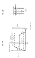
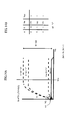
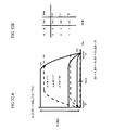
- Figs. 12A through 14B show the operating point V m with respect to each parameter ⁇ .
- Figs. 12A through 12C the AND/OR function is described.
- the circuit has the same structure as that of the circuit shown in Fig. 7, and the AND(Fig. 12C)/OR(Fig. 12B) function can be maintained.
- the transistor Tr5 is regarded as open, and accordingly, functions as an AND circuit.
- V out becomes "1" for all the inputs (see Figs. 14A and 14B).
- This circuit is characterized in that the operating point V m is always close to 0V or V dd , and the logic margin is wide.
- a logic circuit in accordance with this embodiment can be formed by using a spin MOSFET for either the n-channel MOSFET or the p-channel MOSFET in a CMOS inverter, or using spin MOSFETs for both the n-channel MOSFET and the p-channel MOSFET.
- the ⁇ MOS structure used for the input is formed with a floating gate shared by the n-channel device and the p-channel device.
- the inverter of the output stage is a conventional inverter of the CMOS configuration.
- the operating curve is saturated as in the E/D configuration, and accordingly, the mean logic margin can be made wider. Also, it is effective for low power consumption.
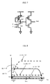
- Fig. 16A is a circuit diagram of an inverter having a variable logic threshold value.
- the n-channel MOSFET and the p-channel MOSFET of a conventional CMOS inverter are replaced with a p-channel spin MOSFET.
- the current driving capacity of the n-channel spin MOSFET is a value between 1 and 10.
- the logic threshold value of the inverter circuit shown in Fig. 16A varies according to the combination of parameters ⁇ . Fig.
- 16B shows the characteristics of both spin MOSFETs in a case where the parameter ⁇ ninv is fixed while the parameter ⁇ pinv is set to 1 or 10.
- the output V out is V L of the low level when the parameter ⁇ pinv is 1
- the output V out is V H of the high level when the parameter ⁇ pinv is 10.
- the output V out varies according to the current driving capacity of the p-channel spin MOSFET. More quantitatively, this can be explained as follows.
- the inverter circuit shown in Fig. 16A can be considered as the same as a conventional CMOS inverter.
- the p-channel spin MOSFET and the n-channel spin MOSFET operate in the saturation region.
- I d drain current flowing through the n-channel spin MOSFET and the p-channel spin MOSFET
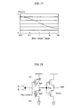
- 0.5V. As shown in Fig. 17, the threshold value according to the ratio ⁇ inv 0.1, 1, 10 can be obtained.
- Fig. 18 illustrates an AND/OR circuit that employs the threshold value variable inverter shown in Fig. 16A.
- the AND/OR circuit is formed with inverters of two stages.
- the inverter at the input side is a threshold value variable inverter
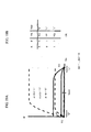
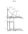
- the operating characteristics of the circuit shown in Fig. 18 are shown in Figs. 19A and 19B.
- the solid line indicates the characteristics of the transistor Tr1
- the broken line indicates the characteristics of the transistor Tr2.
- Table 4 The details of the operation of this circuit are shown in Table 4.
- the operating point V m is V Q , and the output V out is "1".
- the threshold value V inv1 of the threshold value variable inverter (formed with the transistors Tr1 and Tr2) at the input side may be regarded as the reference value. In the following, the operation in such a case is described.
- V fg is V dd .
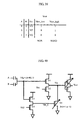
- Fig. 24 illustrates an AND/OR/XNOR circuit.
- the principles of the operation are the same as in the case of the circuit shown in Fig. 10.
- This function can be realized by adding a circuit formed with the transistors Tr3, Tr4, and Tr5 (an n-channel spin MOSFET) to the circuit group Q.
- the inverter (a level shifter) formed with the transistors Tr3 and Tr4 has a threshold value V inv3 lower than V dd /2.
- the transistor Tr5 is equivalent to an open circuit, and operates in the same manner as the AND circuit.
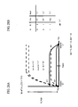
- the output V out becomes "1" for all the input patterns (see Figs. 28A and 28B).
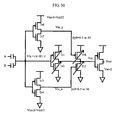
- Fig. 30 illustrates an AND/OR/XNOR/XOR circuit.
- the XOR function can be achieved by employing the transistors Tr6, Tr7, and Tr8 (a p-channel spin MOSFET) in a complementary manner together with the transistors Tr3, Tr4, and Tr5 (an n-channel spin MOSFET).
- the sum of currents flowing through the transistors Tr1 and Tr8 is indicated by solid lines, and the sum of currents flowing through the transistors Tr2 and Tr5 is indicated by broken lines.
- the current I d_low is ignored.
- V out becomes "0".
- the output V out becomes "0" for all the input patterns (see Figs. 33A and 33B).
- an inverter may be added to the output of the circuit shown in Fig. 24.
- the operations of the circuits are shown in Table 7.
- the number of MOSFETs is 10, and the number of capacitors is 2.
- the circuit layout can be made very compact.
- Fig. 36 shows a circuit in which CMOS inverters using spin MOSFETs are connected in two stages.
- Each of the first-stage inverter and the second-stage inverter has an input of a ⁇ MOS structure.
- the same weighting is set on inputs A and B.
- the inputs A and B are input to the second-stage inverter, and the output V m1 of the first stage is also input to the second-stage inverter.
- the capacitance weighting is the same between the inputs A and B in the second-stage inverter, but the capacitance weighting differs between the input A (or B) and the output V m1 .
- CMOS inverter or the like is added to each output to amplify the signal. In such a case, however, the logic function is inverted. Also, it is possible to employ a spin MOSFET for Q2.
- a threshold value variable inverter is employed as the output-stage inverter, so as to form a rewritable logic circuit.
- a logic threshold value V inv is a binary value (V inv_high or V inv_low ), and is supplied through an inverter that includes a conventional nMOS and a p-channel spin MOSFET.
- This inverter functions as an A-D converter that amplifies an analog voltage ("1/2" as described below) to a digital logic level (“0" or "1”), but also controls the threshold value.
- the output-stage A-D converter can be realized by employed the logic threshold value variable inverter, with the spin MOSFETs of the E/E, E/D, and CMOS inverters (shown in Fig. 6) having the ⁇ MOS structure for the inputs being replaced with conventional MOSFETs. In the following, other circuits are described for reference.
- Fig. 37 illustrates an example structure of a NAND/NOR circuit. This circuit differs from the circuit illustrated in Fig. 48, in that the value of Vm is not varied by spin MOSFETs but the threshold value is varied when the threshold value is amplified to the logic level by the inverter.
- the load curve (the characteristics of the ⁇ MOS structure) of the logic circuit shown in Fig. 37 is represented by a single line, and the operating points are indicated only by V O , V P , and V Q .
- the functions are changed by varying the operating point with the logic threshold value V inv that is higher (V inv_high ) or lower (V inv_low ) than the operating point V P when A or B is "1".
- V inv V m V out (in order of Vm) function A B 0 0 0 1 1 1 V inv_low V O ("0") V P ("1/2") V Q ("1") "1" "0” "0” NOR V inv_high V O (“0") V P ("1/2") V Q ("1") "1" "1” "0” NAND
- the circuit functions as a NOR circuit. If the threshold value V inv is equal to V inv_low , the output V out is "0", and accordingly, the circuit functions as a NOR circuit. If the threshold value V inv is equal to V inv_high , the output V out is "1", and accordingly, the circuit functions as a NAND circuit.
- Fig. 40 illustrates a NAND/NOR+XNOR circuit.
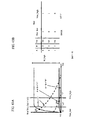
- Fig. 41 shows the operating points of the circuit. The principles of the operation of this circuit are the same as those shown in Figs. 50 through 54.
- Table 9 The details of the operation are shown in Table 9.
- V inv ⁇ n5 V m V out (in order of Vm) function A B 0 0 0 1 1 1 V inv_low 1 V O (“0") V P ("1/2") V Q ("1") "1" “0” “0” NOR V inv_high 1 V O (“0") V P ("1/2") V Q ("1") "1" “1” “0” NAND V inv_low 10 V O (“0”) V P ("1/2") V R (“0”) "1” "0” “1” XNOR V inv_high 10 V O (“0”) V P (“1/2”) V R (“0") "1" "1” “1” all”1”
- the transistor Tr5 is put into the state in which ⁇ n5 is "1", so that the drain current I id_low can be ignored. Accordingly, the transistor Tr5 can be regarded as open, and the circuit becomes equivalent to the NAND/NOR circuit shown in Fig. 37.
- the transistor Tr5 is put into the state in which ⁇ n5 is 10, and the threshold value of the inverter is set at V inv_low as in the NOR circuit.
- the transistor Tr5 is regarded as open, and operates in the same manner as the NOR circuit.
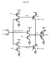
- Fig. 44 illustrates a NAND/NOR/XNOR/XOR circuit.
- the XOR function can be achieved by employing the p-channel transistors Tr6, Tr7, and Tr8 (a p-channel spin MOSFET) in a complementary manner together with the n-channel transistors Tr3, Tr4, and Tr5 (an n-channel spin MOSFET).
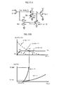
- Fig. 45 shows the operating characteristics of the transistors Tr6 and Tr7. According to the operating characteristics, V in_p is determined.
- Figs. 46A and 46B show the operating points V m in the case where ⁇ p8 is 10 and in the case where ⁇ n5 is 1. The sum of the currents flowing through the transistors Tr1 and Tr8 is indicated by solid lines, and the current I d_low is ignored in Figs. 46A and 46B.
- the transistor Tr8 is put into the state in which ⁇ p8 is 10, and the threshold value of the inverter is set at V inv_high as in the NAND circuit.
- the transistor Tr5 is put into the state in which ⁇ n5 is 1, so as to be open.
- the transistor Tr8 is put into the state in which ⁇ p8 is 10 and the threshold value is set at V inv_low , the output V out becomes "0" for all inputs.
- an OR/AND can be realized with the circuit shown in Fig. 44.
- the number of MOSFETs is 10, and the number of capacitors is 2.
- the spin MOSFETs of two different types having different rates of change in driving force (the rate of change between Tr1 and Tr2 is 10, and the rate of change between Tr5 and Tr8 is 100, for example) need to be integrated in the circuit shown in Fig. 30, the circuit shown in Fig. 44 requires only one type of spin MOSFET.
- this circuit is equivalent to the circuit shown in Fig. 37, and functions as a NOR ciruict with V inv_low , and as a NAND circuit with V inv_high .
- this circuit is equivalent to the circuit shown in Fig. 43, and functions as a XNOR circuit.
- this circuit is equivalent to the circuit shown in Fig. 9B, and functions as a XNOR circuit.
- the value ⁇ n5 is set at 10, and the value ⁇ p8 is set at 10 in the circuit shown in Fig. 44 (see Figs. 47A and 47B).
- the transistors Tr5 and Tr8 are both open, and accordingly, the circuit becomes equivalent to the circuit shown in Fig. 37. Since the relationship V inv_low ⁇ V P ⁇ V inv_high is established, the circuit functions as an AND circuit, with V inv being V inv?low . The circuit functions as an OR circuit, with V inv being V inv_high .
- the above circuit may be of either an n-channel type or a p-channel type, as long as the transistors Tr1 and Tr2 are of the same conductivity type in each circuit diagram.
- This logic circuit employs circuit groups including enhancement MOSFETs and n-channel spin MOSFETs.
- Fig. 48 illustrates an example structure of a rewritable NAND/NOR circuit.
- a rewritable NAND/NOR circuit includes a logic gate stage and an inverter stage.
- the logic gate stage has a series-connection structure in which a ⁇ MOS (Tr1) and a spin MOSFET (Tr2) are connected in series.
- the ⁇ MOS (Tr1) has two inputs A and B, and the voltage V fg to be applied to the floating gate according to the input value is determined by the equation: (A+B)/2, for example.
- the current gain of the ⁇ MOS (Tr1) is represented by ⁇ n1 .
- the inputs are represented by A and B, and the output is represented by V out , which is either "0" (Low level, 0V) or "1" (High level, the source voltage V dd ).
- the above ⁇ MOS (Tr1) functions as a D-A converter that converts a digital input of "0” or “1” to a voltage of 0, V dd /2, or V dd .
- Tr2 is a spin MOSFET (distinguished from a conventional MOSFET by the addition of an arrow), and a constant bias V b is applied to Tr2.
- the static characteristics of the spin MOSFET (Tr2) are shown by the solid line in Fig. 6.
- the ⁇ MOS (Tr1) and the spin MOSFET (Tr2) function as a source follower circuit.
- the ⁇ MOS (Tr1) charges the V m node, which is the connecting point between the ⁇ MOS (Tr1) and the spin MOSFET (Tr2), with the driving force according to V fg .
- the spin MOSFET (Tr2) discharges the V m node with the driving force according to the magnetization state.
- the ⁇ MOS (Tr1) and the spin MOSFET (Tr2) constitute the logic gate.
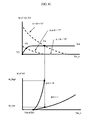
- Fig. 49 shows the load curve according to the ⁇ MOS (Tr1) (indicated by the broken line) and the operating points (V o through V s ) of this logic gate.
- the analog voltage V m supplied at the operating points (V o through V s ) is inverted and amplified to the digital logic level "0" or "1" by an inverter with the characteristics shown in the lower half of Fig. 49, with V inv being the threshold value.
- the analog voltage V m is then output to an output terminal V out .
- Table 12 shows the relationship among ⁇ n2 , the operating points, and the circuit functions.
- the drain current I d is 0.
- the analog voltage V m is V O ⁇ V inv
- the output V out is "1", with the inverting amplification of the A-D converter being taken into consideration.
- V m is V P > V inv
- V out is "0".
- the analog voltage V m is V O ⁇ V inv
- the output V out is "1"
- the inverting amplification of the A-D converter being taken into consideration.
- V m is V Q > V inv
- V out is "0".
- the above outputs do not depend on the driving force ⁇ n2 of the spin MOSFET (Tr2) (not depending on whether the magnetization state is parallel or antiparallel).
- a or B is "1”
- V m is charged by Tr1.
- V m becomes V s > V inv
- V out is "0".
- the circuit functions as a NOR circuit.
- Fig. 50 shows the truth table of the circuit shown in Fig. 48.
- NOR logic or a NAND logic can be selected as the output V out in response to the inputs A and B. Since the magnetization state of the spin MOSFET is stored in a non-volatile manner, a NOR logic or a NAND logic can be selected in a single circuit. If a circuit having such a function is formed with a conventional CMOS digital circuit, ten MOSFETs are necessary. The circuit of this example is advantageous in that the same function can be realized with only four MOSFETs.
- a rewritable NAND/NOR+XNOR circuit is described.
- a circuit that is formed with two conventional nMOSFETs (Tr3 and Tr4) and one n-channel spin MOSFET (Tr5) is added.
- Fig. 51B illustrating the operation, the upper graph shows the operating characteristics of Tr3 and Tr4 in Fig. 8. According to the operating characteristics, V in_n is determined. The static characteristics of Tr4 are indicated by the solid line, and the load curve of Tr3 is indicated by the broken lines.
- Tr5 is turned on. If n-channel spin MOSFETs with threshold values greater than V dd /2 can be integrated, Tr3 and Tr4 are not necessary, and the V fg node should be connected directly to the gate of Tr5. In the case where ⁇ n5 is 10, a sufficiently high current I d_high flows, but in the case where ⁇ n5 is 1, the value of the current (I d_low ) is very small, as can be seen from the lower graph in Fig. 8B.
- Figs. 52A through 54B show the operating points V m with the respective values of ⁇ .
- the sum of the currents flowing through Tr2 and Tr5 is indicated by the solid lines, and the current I d_low is ignored.
- Table 13 collectively shows the relationship between ⁇ n2 , ⁇ n5 , and the functions of the circuit.
- Tr5 when Tr5 is put into the state in which ⁇ n5 is 10 and Tr2 is put into the state in which ⁇ n2 is 10, the output V out becomes "1" for all inputs (all "1"), as shown in Figs. 11A and 11B.
- any of the logic circuits in accordance with the embodiments of the present invention includes a spin transistor or a spin MOSFET that can change the current driving force in a non-volatile manner, and a ⁇ MOS structure.
- a spin transistor or a spin MOSFET that can change the current driving force in a non-volatile manner
- a ⁇ MOS structure In such a structure, symmetric Boolean functions that are reconfigurable in a non-volatile manner can be realized with a small number of devices.
- the chip area can be reduced, and high-speed, low-consumption electric operations can be expected. Accordingly, this circuit can be applied to the integrated circuits for mobile devices that are produced in a short time.
- a logic circuit of the present invention Using a logic circuit of the present invention, symmetric Boolean functions that are reconfigurable in a non-volatile manner can be realized with a smaller number of devices. Since a circuit of the present invention can maintain each logic function in a non-volatile manner, there is no need to employ a non-volatile memory for storing logic functions. Accordingly, the chip size can be reduced. Also, using a circuit with a smaller number of devices, high-speed, low-consumption electric operations can be expected. Thus, the circuits of the present invention can be applied to the integrated circuits for mobile devices that are produced in a short time.
Landscapes
- Engineering & Computer Science (AREA)
- Mathematical Physics (AREA)
- Physics & Mathematics (AREA)
- Computer Hardware Design (AREA)
- Computing Systems (AREA)
- General Engineering & Computer Science (AREA)
- Power Engineering (AREA)
- Logic Circuits (AREA)
- Hall/Mr Elements (AREA)
- Non-Volatile Memory (AREA)
- Insulated Gate Type Field-Effect Transistor (AREA)
- Mram Or Spin Memory Techniques (AREA)
- Design And Manufacture Of Integrated Circuits (AREA)
- Semiconductor Memories (AREA)
Abstract
Description
| βn1 | Vm | Vout (in order of Vm) | function | |||||
| A | 0 0 | 0 1 | 1 1 | |||||
| 1 | VO("1") | VP("0") | VQ("0") | "0" | "1" | "1" | OR | |
| 10 | VO("1") | VR("1") | VS("0") | "0" | "0" | "1" | AND |
| βn1 | βn5 | Vm | Vout (in order of Vm) | function | |||||
| A | 0 0 | 0 1 | 1 1 | ||||||
| 1 | 0.5 | VO("1") | VP("0") | VQ("0") | "0" | "1" | "1" | OR | |
| 10 | 0.5 | VO("1") | VR("1") | VS("0") | "0" | "0" | "1" | AND | |
| 1 | 50 | VT("0") | VR("1") | VS("0") | "1" | "0" | "1" | | |
| 10 | 50 | VU("0") | VR("0") | VV("0") | "1" | "1" | "1" | all"1" |
| βn1 | βn5 | Vout | | function | ||||||
| A | 0 0 | 0 1 | 1 1 | A | 0 0 | 0 1 | 1 1 | |||
| 1 | 0.5 | "0" | "1" | "1" | "1" | "0" | "0" | OR/NOR | ||
| 10 | 0.5 | "0" | "0" | "1" | "1" | "1" | "0" | AND/ | ||
| 1 | 50 | "1" | "0" | "1" | "0" | "1" | "0" | XNOR/ | ||
| 10 | 50 | "1" | "1" | "1" | "0" | "0" | "0" | all"1"/all"0" |
| βn1 | βn2 | Vm | Vout (in order of Vm) | function | |||||
| A | 0 0 | 0 1 | 1 1 | ||||||
| 1 | 10 | VO("1") | VP("0") | VQ("0") | "0" | "1" | "1" | OR | |
| 10 | 1 | VO("1") | VR("1") | VQ("0") | "0" | "0" | "1" | AND |
| βp1 | βn2 | βn5 | Vm | Vout (in order of Vm) | function | |||||
| A | 0 0 | 0 1 | 1 1 | |||||||
| 1 | 10 | 0.5 | VO("1") | Vp("0") | VQ("0") | "0" | "1" | "1" | OR | |
| 10 | 1 | 0.5 | VO("1") | VR("1") | VQ("0") | "0" | "0" | "1" | AND | |
| 1 | 10 | 50 | VT("0") | VP("0") | VQ("0") | "1" | "1" | "1" | all"1" | |
| 10 | 1 | 50 | VS("0") | VR("1") | VQ("0") | "1" | "0" | "1" | XNOR |
| βn1 | βn2 | βn5 | βp8 | Vm | Vout (in order of Vm) | function | |||||
| A | 0 0 | 0 1 | 1 1 | ||||||||
| 1 | 10 | 0.5 | 0.5 | "1" | "0" | "0" | "0" | "1" | "1" | OR | |
| 10 | 1 | 0.5 | 0.5 | "1" | "1" | "0" | "0" | "0" | "1" | AND | |
| 1 | 10 | 50 | 0.5 | "0" | "0" | "0" | "1" | "1" | "1" | all"1" | |
| 10 | 1 | 50 | 0.5 | "0" | "1" | "0" | "1" | "0" | "1" | | |
| 1 | 10 | 0.5 | 50 | VO("1") | VP("0") | VT("1") | "0" | "1" | "0" | | |
| 10 | 1 | 0.5 | 50 | VO("1") | VR("1") | VT("1") | "0" | "0" | "0" | all"0" |
| βn1 | βn2 | βn5 | βp8 | Vm | Vout (in order of Vm) | function | |||||
| A | 0 0 | 0 1 | 1 1 | ||||||||
| 1 | 10 | 0.5 | 0.5 | "1" | "0" | "0" | "0" | "1" | "1" | OR | |
| 10 | 1 | 0.5 | 0.5 | "1" | "1" | "0" | "0" | "0" | "1" | AND | |
| 1 | 10 | 50 | 0.5 | "0" | "0" | "0" | "1" | "1" | "1" | all"1" | |
| 10 | 1 | 50 | 0.5 | "0" | "1" | "0" | "1" | "0" | "1" | | |
| 1 | 10 | 0.5 | 50 | "1" | "0" | "1" | "0" | "1" | "0" | | |
| 10 | 1 | 0.5 | 50 | "1" | "1" | "1" | "0" | "0" | "0" | all"0" | |
| 1 | 10 | 50 | 50 | VT("0") | VP("0") | VU("1") | "1" | "1" | "0" | | |
| 10 | 1 | 50 | 50 | VS("0") | VR("1") | VV("1") | "1" | "0" | "0" | NOR |
| Vinv | Vm | Vout (in order of Vm) | function | |||||
| A | 0 0 | 0 1 | 1 1 | |||||
| Vinv_low | VO("0") | VP("1/2") | VQ("1") | "1" | "0" | "0" | NOR | |
| Vinv_high | VO("0") | VP("1/2") | VQ("1") | "1" | "1" | "0" | NAND |
| Vinv | βn5 | Vm | Vout (in order of Vm) | function | |||||
| A | 0 0 | 0 1 | 1 1 | ||||||
| Vinv_low | 1 | VO("0") | VP("1/2") | VQ("1") | "1" | "0" | "0" | NOR | |
| Vinv_high | 1 | VO("0") | VP("1/2") | VQ("1") | "1" | "1" | "0" | NAND | |
| Vinv_low | 10 | VO("0") | VP("1/2") | VR("0") | "1" | "0" | "1" | XNOR | |
| Vinv_high | 10 | VO("0") | VP("1/2") | VR("0") | "1" | "1" | "1" | all"1" |
| Vinv | βn5 | βp8 | Vm | Vout (in order of Vm) | function | |||||
| A | 0 0 | 0 1 | 1 1 | |||||||
| | 1 | 1 | "0" | "1/2" | "1" | "1" | "0" | "0" | NOR | |
| | 1 | 1 | "0" | "1/2" | "1" | "1" | "1" | "0" | | |
| V | ||||||||||
| inv_low | 10 | 1 | "0" | "1/2" | "0" | "1" | "0" | "1" | | |
| V | ||||||||||
| inv_high | 10 | 1 | "0" | "1/2" | "0" | "1" | "1" | "1" | all"1" | |
| | 1 | 10 | VO("1") | VP("1/2") | VQ("1") | "0" | "0" | "0" | all"0" | |
| | 1 | 10 | VO("1") | VP("1/2") | VQ("1") | "0" | "1" | "0" | XOR |
| Vinv | βn5 | βp8 | Vm | Vout (in order of Vm) | function | |||||
| A | 0 0 | 0 1 | 1 1 | |||||||
| | 1 | 1 | "0" | "1/2" | "1" | "1" | "0" | "0" | NOR | |
| | 1 | 1 | "0" | "1/2" | "1" | "1" | "1" | "0" | | |
| V | ||||||||||
| inv_low | 10 | 1 | "0" | "1/2" | "0" | "1" | "0" | "1" | | |
| V | ||||||||||
| inv_high | 10 | 1 | "0" | "1/2" | "0" | "1" | "1" | "1" | all"1" | |
| | 1 | 10 | "1" | "1/2" | "1" | "0" | "0" | "0" | all"0" | |
| | 1 | 10 | "1" | "1/2" | "1" | "0" | "1" | "0" | | |
| V | ||||||||||
| inv_low | 10 | 10 | VO("1") | VP("1/2") | VR("0") | "0" | "0" | "1" | AND | |
| | 10 | 10 | VO("1") | VP("1/2") | VR("0") | "0" | "1" | "1" | OR |
| βn2 | Vm | Vout (in order of Vm) | function | |||||
| A | 0 0 | 0 1 | 1 1 | |||||
| 1 | VO("0") | VS("1") | VQ("1") | "1" | "0" | "0" | NOR | |
| 10 | VO("0") | VR("0") | VP("1") | "1" | "1" | "0" | NAND |
| βn2 | βn5 | Vm | Vout (in order of Vm) | function | |||||
| A | 0 0 | 0 1 | 1 1 | ||||||
| 1 | 1 | VO("0") | VS("1") | VQ("1") | "1" | "0" | "0" | NOR | |
| 10 | 1 | VO("0") | VR("0") | VP("1") | "1" | "1" | "0" | | |
| 1 | 10 | VO("0") | VS("1") | VU("0") | "1" | "0" | "1" | | |
| 10 | 10 | VO("0") | VR("0") | VV("0") | "1" | "1" | "1" | all"1" |
| βn2 | βn5 | Vout | | function | ||||||
| A | 0 0 | 0 1 | 1 1 | A | 0 0 | 0 1 | 1 1 | |||
| 1 | 1 | "1" | "0" | "0" | "0" | "1" | "1" | NOR/OR | ||
| 10 | 1 | "1" | "1" | "0" | "0" | "0" | "1" | NAND/AND | ||
| 1 | 10 | "1" | "0" | "1" | "0" | "1" | "0" | XNOR/ | ||
| 10 | 10 | "1" | "1" | "1" | "0" | "0" | "0" | all"1"/all"0" |
Claims (45)
- A circuit comprising
a spin transistor having transfer characteristics depending on the spin direction of conduction carriers,
the spin direction of the conduction carriers being changed so as to vary the transfer characteristics of the spin transistor,
an operating point being changed based on the transfer characteristics, thereby reconfiguring a function. - A circuit comprising
a spin transistor that includes at least two ferromagnetic layers, and has transfer characteristics depending on the magnetization state of the ferromagnetic layers,
the magnetization state of the spin transistor being changed to move an operating point, thereby reconfiguring a function. - The circuit as claimed in claim 2, wherein:the spin transistor has at least one ferromagnetic body ("free layer") with a magnetization direction that can be controlled independently, and at least one ferromagnetic body ("pin layer") with a fixed magnetization direction; andthe circuit reconfigures a function by changing an operating point based on two magnetization states including a first state in which the free layer and the pin layer have the same magnetization directions ("parallel magnetization"), and a second state in which the free layer and the pin layer have the opposite magnetizing states to each other ("antiparallel magnetization").
- The circuit as claimed in any of claims 1 to 3, further comprising:wherein the spin transistor is included in one or both of the first circuit group and the second circuit group.a first terminal that generates the operating point and serves as an output;a first circuit group for charging the first terminal; anda second circuit group for discharging the first terminal,
- The circuit as claimed in claim 4, wherein the first terminal has a potential that is determined by changing the spin directions of the carriers of the spin transistor or by controlling the transfer characteristics depending on the magnetization state of the spin transistor.
- The circuit as claimed in any of claims 1 to 5, which outputs a signal based on a signal that is input via a neuron MOS (νMOS) structure including a plurality of inputs weighted with capacitances by capacitors and a floating gate connecting the inputs.
- The circuit as claimed in claim 6, wherein the input signals are weighted so as to be substantially equal to one another.
- The circuit as claimed in any of claims 4 to 7, wherein a logic threshold value for dividing the potential generated in the first terminal into an output of a logic level "0" and an output of a logic level "1" is set with respect to the operating point that varies according to a variation in the transfer characteristics of the spin transistor.
- The circuit as claimed in any of claims 1 to 8, wherein an A-D converter with a predetermined logic threshold value is connected to an output terminal of the circuit.
- The circuit as claimed in any of claims 1 to 9, wherein the spin transistor is a MOSFET-type spin transistor ("spin MOSFET") that are formed with a source and a drain, including a MOS structure and a ferromagnetic body.
- The circuit as claimed in any of claims 3 to 9, wherein the first circuit group includes a MOSFET of a first conductivity type or a spin MOSFET of the first conductivity type, and the second circuit group includes a MOSFET of the same conductivity type as the first conductivity type or a spin MOSFET of the same conductivity type as the first conductivity type.
- The circuit as claimed in any of claims 3 to 11, comprising
an E/E circuit that includes a structure in which the source of an enhancement MOSFET or an enhancement spin MOSFET contained in the first circuit group is connected to the drain of an enhancement MOSFET or an enhancement spin MOSFET contained in the second circuit group, and a first terminal that is formed at the connection portion. - The circuit as claimed in claim 12, wherein the drain of an enhancement MOSFET or an enhancement spin MOSFET contained in the first circuit group in the E/E circuit is connected to the gate of the enhancement MOSFET or the enhancement spin MOSFET.
- The circuit as claimed in claim 12 or 13, wherein an enhancement MOSFET or an enhancement spin MOSFET contained in the second circuit group in the E/E circuit has a νMOS structure.
- The circuit as claimed in any of claims 3 to 11, comprising
an E/D circuit that includes a structure in which the source of a depletion MOSFET or a depletion spin MOSFET contained in the first circuit group is connected to the drain of an enhancement MOSFET or an enhancement spin MOSFET contained in the second circuit group, and a first terminal that is formed at the connection portion. - The circuit as claimed in claim 15, wherein the source of a depletion MOSFET or a depletion spin MOSFET contained in the first circuit group in the E/D circuit is connected to the gate of the depletion MOSFET or the depletion spin MOSFET.
- The circuit as claimed in claim 15 or 16, wherein an enhancement MOSFET or an enhancement spin MOSFET contained in the second circuit group in the E/D circuit has a νMOS structure.
- The circuit as claimed in any of claims 11 to 17, wherein the νMOS structure has two inputs (A and B) weighted with capacitances by capacitors.
- The circuit as claimed in any of claims 4 to 18, wherein the circuit is a NAND/NOR reconfigurable logic circuit or an AND/OR reconfigurable logic circuit that includes the A-D converter having the first terminal as an input.
- The circuit as claimed in any of claims 11 to 19, wherein the first and second circuit groups or one of the first and second circuit groups comprises
a circuit that controls the potential of the first terminal by connecting the source or the drain of another spin MOSFET to the first terminal, and connecting a level shift circuit to the gate of the another spin MOSFET, the level shift circuit turning on the another spin MOSFET only when a predetermined input is made. - The circuit as claimed in any of claims 11 to 20, wherein the second circuit group comprises
a circuit that controls the potential of the first terminal by connecting the drain of another spin MOSFET of n-channel type to the first terminal, and connecting a level shift circuit to the gate of the another spin MOSFET of n-channel type, the another spin MOSFET of n-channel having the source grounded, the level shift circuit turning on the another spin MOSFET of n-channel type only when an input is A = B = "0". - The circuit as claimed in any of claims 11 to 21, wherein the first circuit group comprises
a circuit that controls the potential of the first terminal by connecting the drain of another spin MOSFET of p-channel type to the first terminal, and connecting a level shift circuit to the gate of the another spin MOSFET of p-channel type, the another spin MOSFET of p-channel having the source connected to a supply voltage, the level shift circuit turning on the another spin MOSFET of p-channel type only when an input is A = B = "1". - The circuit as claimed in any of claims 20 to 23, wherein the level shift circuit is formed with an E/E, E/D, or CMOS inverter.
- The circuit as claimed in any of claims 20 to 23, wherein the circuit is a reconfigurable logic circuit that includes the A-D converter having the first terminal as an input.
- The circuit as claimed in claim 20 or 24, wherein the circuit is a reconfigurable logic circuit that includes an inverter having the output of the A-D converter as an input, and can achieve all symmetric Boolean functions.
- The circuit as claimed in any of claims 3 to 9, wherein the first circuit group includes a MOSFET of a first conductivity type or a spin MOSFET of the first conductivity type, and the second circuit group includes a MOSFET of a second conductivity type different from the first conductivity type or a spin MOSFET of the second conductivity type.
- The circuit as claimed in claim 26, comprising
a CMOS circuit that includes a structure in which a p-channel MOSFET or a p-channel spin MOSFET contained in the first circuit group is connected to an n-channel MOSFET or an n-channel spin MOSFET contained in the second circuit group with a shared drain terminal, and a first terminal that is formed at the shared drain terminal. - The circuit as claimed in claim 26, comprising
a CMOS circuit that is formed with a p-channel spin MOSFET contained in the first circuit group and an n-channel spin MOSFET contained in the second circuit group. - The circuit as claimed in any of claims 26 to 28, wherein the p-channel MOSFET or the p-channel spin MOSFET, and the n-channel MOSFET or the n-channel spin MOSFET of the CMOS circuit have a shared floating gate forming a νMOS structure.
- The circuit as claimed in claim 29, wherein the νMOS structure has two inputs (A and B) weighted with capacitances by capacitors.
- The circuit as claimed in any of claims 26 to 30, wherein the circuit is an AND/OR reconfigurable logic circuit or a NAND/NOR reconfigurable logic circuit that includes an A-D converter having the first terminal as an input.
- The circuit as claimed in any of claims 26 to 31, wherein the first and second circuit groups, or one of the first and second circuit groups comprises
a circuit that controls the potential of the first terminal by connecting the source or the drain of another spin MOSFET to the first terminal, and connecting a level shift circuit to the gate of the another spin MOSFET, the level shift circuit turning on the another spin MOSFET only when a predetermined input is made. - The circuit as claimed in any of claims 26 to 32, wherein the second circuit group comprises
a circuit that controls the potential of the first terminal by connecting the drain of another spin MOSFET of n-channel type to the first terminal, and connecting a level shift circuit to the gate of the another spin MOSFET of n-channel type, the another spin MOSFET of n-channel having the source grounded, the level shift circuit turning on the another spin MOSFET of n-channel type only when an input is A = B = "0". - The circuit as claimed in any of claims 26 to 33, wherein the circuit is an AND/OR/XNOR reconfigurable logic circuit or a NAND/NOR/XOR reconfigurable logic circuit that includes an A-D converter having the first terminal as an input.
- The circuit as claimed in any of claims 26 to 35, wherein the first circuit group comprises
a circuit that controls the potential of the first terminal by connecting the drain of the another spin MOSFET of p-channel type to the first terminal, and connecting a level shift circuit to the gate of the another spin MOSFET of p-channel type, the another spin MOSFET of p-channel having the source connected to a supply voltage, the level shift circuit turning on the another spin MOSFET of p-channel type only when an input is A = B = "1". - The circuit as claimed in any of claims 26 to 35, wherein the circuit is an AND/OR/XOR reconfigurable logic circuit or a NAND/NOR/XNOR reconfigurable logic circuit that includes an A-D converter having the first terminal as an input.
- The circuit as claimed in any of claims 26 to 36, wherein the circuit is a reconfigurable logic circuit that includes an inverter having the output of the A-D converter as an input, and can achieve all symmetric Boolean functions.
- The circuit as claimed in claim 26 or 32, wherein the circuit is formed with a circuit group that is characterized by:controlling the potential of the first terminal by connecting the drain of another spin MOSFET of n-channel type to the first terminal, and connecting a level shift circuit to the gate of the another spin MOSFET of n-channel type, the another spin MOSFET of n-channel having the source grounded, the level shift circuit turning on the another spin MOSFET of n-channel type only when an input is A = B = "1"; andcontrolling the potential of the first terminal by connecting the drain of another spin MOSFET of p-channel type to the first terminal, and connecting a level shift circuit to the gate of the another spin MOSFET of p-channel type, the another spin MOSFET of p-channel having the source connected to a supply voltage, the level shift circuit turning on the another spin MOSFET of p-channel type only when an input is A = B = "0".
- The circuit as claimed in claim 38, wherein the circuit is an all symmetric Boolean function logic circuit that includes an A-D converter having the first terminal as an input.
- The circuit as claimed in any of claims 32 to 39, wherein the level shift circuit is formed with an E/E, E/D, or CMOS inverter.
- An A-D converter comprising
a CMOS inverter,
one of a p-channel MOSFET or an n-channel MOSFET of the CMOS inverter being a spin MOSFET, or a p-channel MOSFET and an n-channel MOSFET of the CMOS inverter being spin MOSFETs. - The A-D converter as claimed in claim 41, wherein a logic threshold value can be changed according to the magnetization state of the spin MOSFET.
- A logic circuit comprising
an A-D converter that has a variable logic threshold value and is connected to an output stage of a circuit having an analog output, the logic circuit being capable of reconfiguring a logic function. - A circuit comprising
a transistor with variable transfer characteristics,
the circuit being capable of reconfiguring a function by moving an operating point through a change in the transfer characteristics of the transistor. - An integrated circuit comprising
the circuit as claimed in any of claims 1 to 44.
Applications Claiming Priority (3)
| Application Number | Priority Date | Filing Date | Title |
|---|---|---|---|
| JP2003086499 | 2003-03-26 | ||
| JP2003086499 | 2003-03-26 | ||
| PCT/JP2004/004379 WO2004086625A1 (en) | 2003-03-26 | 2004-03-26 | Reconfigurable logical circuit using transistor having spin-dependent transmission characteristic |
Publications (2)
| Publication Number | Publication Date |
|---|---|
| EP1608071A1 true EP1608071A1 (en) | 2005-12-21 |
| EP1608071A4 EP1608071A4 (en) | 2006-05-24 |
Family
ID=33095067
Family Applications (1)
| Application Number | Title | Priority Date | Filing Date |
|---|---|---|---|
| EP04723782A Withdrawn EP1608071A4 (en) | 2003-03-26 | 2004-03-26 | RECONFIGURABLE LOGIC CIRCUIT USING A TRANSISTOR HAVING SPIN DEPENDENT TRANSMISSION CHARACTERISTICS |
Country Status (7)
| Country | Link |
|---|---|
| US (1) | US7545013B2 (en) |
| EP (1) | EP1608071A4 (en) |
| JP (1) | JP4143644B2 (en) |
| KR (1) | KR100789044B1 (en) |
| CN (1) | CN1333528C (en) |
| TW (1) | TW200503420A (en) |
| WO (1) | WO2004086625A1 (en) |
Cited By (2)
| Publication number | Priority date | Publication date | Assignee | Title |
|---|---|---|---|---|
| EP3435433A1 (en) * | 2017-07-27 | 2019-01-30 | Korea Institute of Science and Technology | Reconfigureable logic device using electrochemical potential |
| US10424379B2 (en) | 2017-12-01 | 2019-09-24 | Namlab Ggmbh | Polarization-based configurable logic gate |
Families Citing this family (41)
| Publication number | Priority date | Publication date | Assignee | Title |
|---|---|---|---|---|
| JP4744934B2 (en) * | 2004-06-16 | 2011-08-10 | 株式会社東芝 | Spin transistor |
| US7411235B2 (en) | 2004-06-16 | 2008-08-12 | Kabushiki Kaisha Toshiba | Spin transistor, programmable logic circuit, and magnetic memory |
| JP4528660B2 (en) * | 2005-03-31 | 2010-08-18 | 株式会社東芝 | Spin injection FET |
| JP4599259B2 (en) * | 2005-09-20 | 2010-12-15 | 株式会社東芝 | Magnetic element and magnetic signal processing apparatus using the same |
| JP4675863B2 (en) * | 2006-08-31 | 2011-04-27 | 株式会社東芝 | Programmable logic circuit |
| US20080315917A1 (en) * | 2007-06-21 | 2008-12-25 | Micron Technology, Inc. | Programmable computing array |
| JP4496242B2 (en) * | 2007-08-29 | 2010-07-07 | 株式会社東芝 | Spin transistor and magnetic memory |
| JP2009064826A (en) * | 2007-09-04 | 2009-03-26 | Tdk Corp | Spin transistor and manufacturing method thereof |
| JP4435236B2 (en) * | 2008-01-11 | 2010-03-17 | 株式会社東芝 | Reconfigurable logic circuit |
| JP5017135B2 (en) * | 2008-02-07 | 2012-09-05 | 株式会社東芝 | Semiconductor device |
| JP4516137B2 (en) | 2008-03-27 | 2010-08-04 | 株式会社東芝 | Semiconductor integrated circuit |
| JP4792093B2 (en) * | 2009-02-23 | 2011-10-12 | 株式会社東芝 | Switching box circuit, switching block circuit, and FPGA circuit |
| JP5248446B2 (en) * | 2009-08-18 | 2013-07-31 | 独立行政法人科学技術振興機構 | Electronic circuit |
| KR101016437B1 (en) * | 2009-08-21 | 2011-02-21 | 한국과학기술연구원 | Multifunctional Logic Devices Using Spin Accumulation and Diffusion |
| JP5603049B2 (en) * | 2009-10-28 | 2014-10-08 | 国立大学法人東北大学 | Electronic circuit |
| JP5023167B2 (en) * | 2010-02-08 | 2012-09-12 | 株式会社東芝 | Nonvolatile memory circuit using spin MOS transistor |
| WO2011111305A1 (en) * | 2010-03-10 | 2011-09-15 | パナソニック株式会社 | Method for driving a nonvolatile logic circuit as an exclusive-or circuit |
| JP2011222546A (en) | 2010-04-02 | 2011-11-04 | Tdk Corp | Spin conduction element |
| CN102742160B (en) | 2010-05-11 | 2014-12-17 | 松下电器产业株式会社 | Method for driving non-volatile logic circuit |
| CN102742162B (en) * | 2010-05-11 | 2015-03-25 | 松下电器产业株式会社 | Method for driving non-volatile logic circuit |
| KR101084019B1 (en) | 2010-05-12 | 2011-11-16 | 한국과학기술연구원 | Complementary Spin Transistor Logic Circuit |
| JP2011243716A (en) * | 2010-05-18 | 2011-12-01 | Toshiba Corp | Spin transistor and integrated circuit |
| WO2012029211A1 (en) * | 2010-09-02 | 2012-03-08 | パナソニック株式会社 | Method for driving non-volatile logic circuit |
| CN102598511B (en) * | 2010-11-04 | 2016-01-20 | 松下电器产业株式会社 | The method of non-volatile logic circuit and driving non-volatile logic circuit |
| US8427202B2 (en) | 2010-11-04 | 2013-04-23 | Panasonic Corporation | Nonvolatile logic circuit and a method for operating the same |
| JP5633384B2 (en) | 2011-01-19 | 2014-12-03 | Tdk株式会社 | Spin transport element |
| US8207757B1 (en) * | 2011-02-07 | 2012-06-26 | GlobalFoundries, Inc. | Nonvolatile CMOS-compatible logic circuits and related operating methods |
| JP2012190951A (en) * | 2011-03-10 | 2012-10-04 | Sony Corp | Solid-state imaging device and camera |
| JP5655646B2 (en) * | 2011-03-11 | 2015-01-21 | Tdk株式会社 | Spin device, magnetic sensor and spin FET using the same |
| JP5225419B2 (en) * | 2011-03-28 | 2013-07-03 | 株式会社東芝 | Memory circuit using spin MOSFET, pass transistor circuit with memory function, switching box circuit, switching block circuit, and field programmable gate array |
| US8508256B2 (en) * | 2011-05-20 | 2013-08-13 | Semiconductor Energy Laboratory Co., Ltd. | Semiconductor integrated circuit |
| US9270277B2 (en) * | 2012-06-28 | 2016-02-23 | Northwestern University | Emitter-coupled spin-transistor logic |
| KR101906966B1 (en) | 2012-11-05 | 2018-12-07 | 삼성전자주식회사 | Logic device and operating method of the same |
| JP6037050B2 (en) | 2013-11-20 | 2016-11-30 | Tdk株式会社 | Magnetoresistive element, Spin-MOSFET, magnetic sensor, and magnetic head |
| CN105745761B (en) | 2013-11-20 | 2019-04-09 | Tdk株式会社 | Magnetoresistive effect elements, spin MOSFETs and spin conduction elements |
| US10461751B2 (en) * | 2018-03-08 | 2019-10-29 | Samsung Electronics Co., Ltd. | FE-FET-based XNOR cell usable in neuromorphic computing |
| CN110634516B (en) * | 2018-11-16 | 2021-10-01 | 中山大学 | Programmable Multifunction Spin Logic Adder/Subtracter |
| CN110708058B (en) * | 2019-10-24 | 2023-05-30 | 大连东软信息学院 | 2-4 line decoder based on all-spin logic device and control method thereof |
| US11165430B1 (en) * | 2020-12-21 | 2021-11-02 | Kepler Computing Inc. | Majority logic gate based sequential circuit |
| JP7541190B2 (en) | 2022-01-10 | 2024-08-27 | 之江実験室 | Method, unit and circuit for implementing Boolean logic using compute-in-memory transistors |
| KR20240011992A (en) | 2022-07-20 | 2024-01-29 | 현대자동차주식회사 | Spin-orbit torque array device manufacturing method thereof |
Family Cites Families (14)
| Publication number | Priority date | Publication date | Assignee | Title |
|---|---|---|---|---|
| JPS61234623A (en) | 1985-04-10 | 1986-10-18 | Nec Ic Microcomput Syst Ltd | Nand-nor logic converting circuit |
| JPH05343984A (en) | 1992-06-05 | 1993-12-24 | Oki Micro Design Miyazaki:Kk | Equivalent input level logic circuit |
| JPH06250994A (en) | 1993-02-22 | 1994-09-09 | Sunao Shibata | Arithmetic unit |
| JP3278080B2 (en) * | 1993-02-22 | 2002-04-30 | 直 柴田 | Semiconductor integrated circuit |
| US5654566A (en) * | 1995-04-21 | 1997-08-05 | Johnson; Mark B. | Magnetic spin injected field effect transistor and method of operation |
| US5652445A (en) | 1995-04-21 | 1997-07-29 | Johnson; Mark B. | Hybrid hall effect device and method of operation |
| JP3337599B2 (en) | 1995-07-24 | 2002-10-21 | 株式会社リコー | Semiconductor device, inverter circuit, comparator, and A / D converter circuit |
| JPH11340542A (en) | 1998-05-27 | 1999-12-10 | Sanyo Electric Co Ltd | Magnetoresistance effect device |
| JP3560849B2 (en) * | 1999-06-01 | 2004-09-02 | 日本電信電話株式会社 | Low power consumption type neuron MOS circuit |
| JP2002246487A (en) | 2001-02-16 | 2002-08-30 | Sunao Shibata | Semiconductor device and semiconductor operation device |
| JP2003060211A (en) * | 2001-06-06 | 2003-02-28 | Hokkaido Univ | Spin device and manufacturing method thereof |
| JP2003008105A (en) * | 2001-06-25 | 2003-01-10 | Matsushita Electric Ind Co Ltd | Magnetic resistance element and magnetic memory |
| JP3621367B2 (en) | 2001-09-17 | 2005-02-16 | 株式会社東芝 | Spin transistor |
| JP2008038105A (en) * | 2006-08-10 | 2008-02-21 | Fujitsu Ltd | Adhesive, adhesive sheet, and workpiece peeling method |
-
2004
- 2004-03-26 EP EP04723782A patent/EP1608071A4/en not_active Withdrawn
- 2004-03-26 JP JP2005504130A patent/JP4143644B2/en not_active Expired - Fee Related
- 2004-03-26 TW TW093108244A patent/TW200503420A/en not_active IP Right Cessation
- 2004-03-26 CN CNB2004800081037A patent/CN1333528C/en not_active Expired - Fee Related
- 2004-03-26 WO PCT/JP2004/004379 patent/WO2004086625A1/en not_active Ceased
- 2004-03-26 KR KR1020057017848A patent/KR100789044B1/en not_active Expired - Fee Related
- 2004-03-26 US US10/550,652 patent/US7545013B2/en not_active Expired - Fee Related
Cited By (4)
| Publication number | Priority date | Publication date | Assignee | Title |
|---|---|---|---|---|
| EP3435433A1 (en) * | 2017-07-27 | 2019-01-30 | Korea Institute of Science and Technology | Reconfigureable logic device using electrochemical potential |
| US20190035943A1 (en) * | 2017-07-27 | 2019-01-31 | Korea Institute Of Science And Technology | Reconfigurable logic device using electrochemical potential |
| US10622490B2 (en) | 2017-07-27 | 2020-04-14 | Korea Institute Of Science And Technology | Reconfigurable logic device using electrochemical potential |
| US10424379B2 (en) | 2017-12-01 | 2019-09-24 | Namlab Ggmbh | Polarization-based configurable logic gate |
Also Published As
| Publication number | Publication date |
|---|---|
| TW200503420A (en) | 2005-01-16 |
| US20060114018A1 (en) | 2006-06-01 |
| US7545013B2 (en) | 2009-06-09 |
| EP1608071A4 (en) | 2006-05-24 |
| WO2004086625A1 (en) | 2004-10-07 |
| JPWO2004086625A1 (en) | 2006-06-29 |
| TWI321903B (en) | 2010-03-11 |
| KR100789044B1 (en) | 2007-12-26 |
| JP4143644B2 (en) | 2008-09-03 |
| CN1333528C (en) | 2007-08-22 |
| CN1765054A (en) | 2006-04-26 |
| KR20050111398A (en) | 2005-11-24 |
Similar Documents
| Publication | Publication Date | Title |
|---|---|---|
| US7545013B2 (en) | Reconfigurable logic circuit using a transistor having spin-dependent transfer characteristics | |
| CN113593623B (en) | Analog content addressable memory using three-terminal memory device | |
| US6809957B2 (en) | Memory cells enhanced for resistance to single event upset | |
| US3911289A (en) | MOS type semiconductor IC device | |
| US7428164B2 (en) | Semiconductor memory device | |
| US5581501A (en) | Nonvolatile SRAM cells and cell arrays | |
| US5394034A (en) | Programmable logic array having programmable output driver drive capacity | |
| US6838924B1 (en) | Dual stage level shifter for low voltage operation | |
| US20080151600A1 (en) | Logical Operation Circuit and Logical Operation Device | |
| Matsuno et al. | Novel reconfigurable logic gates using spin metal–oxide–semiconductor field-effect transistors | |
| WO1996030855A1 (en) | Semiconductor arithmetic circuit | |
| KR20230109787A (en) | Compute-in-memory bitcell with capacitively coupled write operation | |
| JPS62124692A (en) | Field effect semiconductor integrated circuit | |
| US5457653A (en) | Technique to prevent deprogramming a floating gate transistor used to directly switch a large electrical signal | |
| WO2009020787A1 (en) | Programmable logic devices comprising junction field effect transistors, and methods of using the same | |
| JPH05291929A (en) | Semiconductor circuit | |
| JPH0556048B2 (en) | ||
| JPH1139879A (en) | Semiconductor device | |
| US7138651B2 (en) | Logic apparatus and logic circuit | |
| US6396168B2 (en) | Programmable logic arrays | |
| US11354098B2 (en) | Configurable non-volatile arithmetic memory operators | |
| US6167560A (en) | One-cold encoding method for low power operation in a complex programmable logic device | |
| Azmine et al. | An advanced 1-bit arithmetic logic unit (ALU) with hybrid memristor-CMOS architecture | |
| KR102303639B1 (en) | MULTIFUNCTIONAL LOGIC STRUCTURE BASED ON Fe-FET | |
| US8633731B1 (en) | Programmable integrated circuit with thin-oxide passgates |
Legal Events
| Date | Code | Title | Description |
|---|---|---|---|
| PUAI | Public reference made under article 153(3) epc to a published international application that has entered the european phase |
Free format text: ORIGINAL CODE: 0009012 |
|
| 17P | Request for examination filed |
Effective date: 20051019 |
|
| AK | Designated contracting states |
Kind code of ref document: A1 Designated state(s): AT BE BG CH CY CZ DE DK EE ES FI FR GB GR HU IE IT LI LU MC NL PL PT RO SE SI SK TR |
|
| AX | Request for extension of the european patent |
Extension state: AL LT LV MK |
|
| RAP1 | Party data changed (applicant data changed or rights of an application transferred) |
Owner name: JAPAN SCIENCE AND TECHNOLOGY AGENCY |
|
| A4 | Supplementary search report drawn up and despatched |
Effective date: 20060406 |
|
| RIC1 | Information provided on ipc code assigned before grant |
Ipc: H01L 29/82 20060101ALI20060401BHEP Ipc: H03K 19/20 20060101AFI20041014BHEP |
|
| DAX | Request for extension of the european patent (deleted) | ||
| RBV | Designated contracting states (corrected) |
Designated state(s): DE FR GB |
|
| RIN1 | Information on inventor provided before grant (corrected) |
Inventor name: TANAKA, MASAAKI Inventor name: MATSUNO, TOMOHIRO Inventor name: SUGAHARA, SATOSHI |
|
| RIN1 | Information on inventor provided before grant (corrected) |
Inventor name: TANAKA, MASAAKI Inventor name: MATSUNO, TOMOHIRO Inventor name: SUGAHARA, SATOSHI |
|
| 17Q | First examination report despatched |
Effective date: 20070507 |
|
| RIC1 | Information provided on ipc code assigned before grant |
Ipc: H01L 29/66 20060101ALI20120321BHEP Ipc: H01L 29/82 20060101ALI20120321BHEP Ipc: H03K 19/0944 20060101AFI20120321BHEP |
|
| GRAP | Despatch of communication of intention to grant a patent |
Free format text: ORIGINAL CODE: EPIDOSNIGR1 |
|
| STAA | Information on the status of an ep patent application or granted ep patent |
Free format text: STATUS: THE APPLICATION IS DEEMED TO BE WITHDRAWN |
|
| 18D | Application deemed to be withdrawn |
Effective date: 20120907 |