EP1605076A2 - Verfahren zur Verhinderung der Kontamination während der Herstellung einer Halbleitervorrichtung - Google Patents
Verfahren zur Verhinderung der Kontamination während der Herstellung einer Halbleitervorrichtung Download PDFInfo
- Publication number
- EP1605076A2 EP1605076A2 EP05018537A EP05018537A EP1605076A2 EP 1605076 A2 EP1605076 A2 EP 1605076A2 EP 05018537 A EP05018537 A EP 05018537A EP 05018537 A EP05018537 A EP 05018537A EP 1605076 A2 EP1605076 A2 EP 1605076A2
- Authority
- EP
- European Patent Office
- Prior art keywords
- film
- substrate
- layer
- semiconductor device
- semiconductor
- Prior art date
- Legal status (The legal status is an assumption and is not a legal conclusion. Google has not performed a legal analysis and makes no representation as to the accuracy of the status listed.)
- Withdrawn
Links
Images




Classifications
-
- H—ELECTRICITY
- H10—SEMICONDUCTOR DEVICES; ELECTRIC SOLID-STATE DEVICES NOT OTHERWISE PROVIDED FOR
- H10P—GENERIC PROCESSES OR APPARATUS FOR THE MANUFACTURE OR TREATMENT OF DEVICES COVERED BY CLASS H10
- H10P70/00—Cleaning of wafers, substrates or parts of devices
- H10P70/50—Cleaning of wafers, substrates or parts of devices characterised by the part to be cleaned
- H10P70/56—Cleaning of wafer backside
-
- H—ELECTRICITY
- H10—SEMICONDUCTOR DEVICES; ELECTRIC SOLID-STATE DEVICES NOT OTHERWISE PROVIDED FOR
- H10D—INORGANIC ELECTRIC SEMICONDUCTOR DEVICES
- H10D10/00—Bipolar junction transistors [BJT]
- H10D10/01—Manufacture or treatment
- H10D10/021—Manufacture or treatment of heterojunction BJTs [HBT]
-
- H—ELECTRICITY
- H10—SEMICONDUCTOR DEVICES; ELECTRIC SOLID-STATE DEVICES NOT OTHERWISE PROVIDED FOR
- H10P—GENERIC PROCESSES OR APPARATUS FOR THE MANUFACTURE OR TREATMENT OF DEVICES COVERED BY CLASS H10
- H10P14/00—Formation of materials, e.g. in the shape of layers or pillars
- H10P14/20—Formation of materials, e.g. in the shape of layers or pillars of semiconductor materials
- H10P14/27—Formation of materials, e.g. in the shape of layers or pillars of semiconductor materials using selective deposition, e.g. simultaneous growth of monocrystalline and non-monocrystalline semiconductor materials
- H10P14/271—Formation of materials, e.g. in the shape of layers or pillars of semiconductor materials using selective deposition, e.g. simultaneous growth of monocrystalline and non-monocrystalline semiconductor materials characterised by the preparation of substrate for selective deposition
-
- H—ELECTRICITY
- H10—SEMICONDUCTOR DEVICES; ELECTRIC SOLID-STATE DEVICES NOT OTHERWISE PROVIDED FOR
- H10P—GENERIC PROCESSES OR APPARATUS FOR THE MANUFACTURE OR TREATMENT OF DEVICES COVERED BY CLASS H10
- H10P14/00—Formation of materials, e.g. in the shape of layers or pillars
- H10P14/20—Formation of materials, e.g. in the shape of layers or pillars of semiconductor materials
- H10P14/29—Formation of materials, e.g. in the shape of layers or pillars of semiconductor materials characterised by the substrates
- H10P14/2901—Materials
- H10P14/2902—Materials being Group IVA materials
- H10P14/2905—Silicon, silicon germanium or germanium
-
- H—ELECTRICITY
- H10—SEMICONDUCTOR DEVICES; ELECTRIC SOLID-STATE DEVICES NOT OTHERWISE PROVIDED FOR
- H10P—GENERIC PROCESSES OR APPARATUS FOR THE MANUFACTURE OR TREATMENT OF DEVICES COVERED BY CLASS H10
- H10P14/00—Formation of materials, e.g. in the shape of layers or pillars
- H10P14/20—Formation of materials, e.g. in the shape of layers or pillars of semiconductor materials
- H10P14/32—Formation of materials, e.g. in the shape of layers or pillars of semiconductor materials characterised by intermediate layers between substrates and deposited layers
- H10P14/3202—Materials thereof
- H10P14/3204—Materials thereof being Group IVA semiconducting materials
- H10P14/3211—Silicon, silicon germanium or germanium
-
- H—ELECTRICITY
- H10—SEMICONDUCTOR DEVICES; ELECTRIC SOLID-STATE DEVICES NOT OTHERWISE PROVIDED FOR
- H10P—GENERIC PROCESSES OR APPARATUS FOR THE MANUFACTURE OR TREATMENT OF DEVICES COVERED BY CLASS H10
- H10P14/00—Formation of materials, e.g. in the shape of layers or pillars
- H10P14/20—Formation of materials, e.g. in the shape of layers or pillars of semiconductor materials
- H10P14/34—Deposited materials, e.g. layers
- H10P14/3402—Deposited materials, e.g. layers characterised by the chemical composition
- H10P14/3404—Deposited materials, e.g. layers characterised by the chemical composition being Group IVA materials
- H10P14/3411—Silicon, silicon germanium or germanium
-
- H—ELECTRICITY
- H10—SEMICONDUCTOR DEVICES; ELECTRIC SOLID-STATE DEVICES NOT OTHERWISE PROVIDED FOR
- H10P—GENERIC PROCESSES OR APPARATUS FOR THE MANUFACTURE OR TREATMENT OF DEVICES COVERED BY CLASS H10
- H10P50/00—Etching of wafers, substrates or parts of devices
- H10P50/60—Wet etching
- H10P50/66—Wet etching of conductive or resistive materials
- H10P50/663—Wet etching of conductive or resistive materials by chemical means only
- H10P50/667—Wet etching of conductive or resistive materials by chemical means only by liquid etching only
-
- H—ELECTRICITY
- H10—SEMICONDUCTOR DEVICES; ELECTRIC SOLID-STATE DEVICES NOT OTHERWISE PROVIDED FOR
- H10P—GENERIC PROCESSES OR APPARATUS FOR THE MANUFACTURE OR TREATMENT OF DEVICES COVERED BY CLASS H10
- H10P70/00—Cleaning of wafers, substrates or parts of devices
- H10P70/10—Cleaning before device manufacture, i.e. Begin-Of-Line process
- H10P70/15—Cleaning before device manufacture, i.e. Begin-Of-Line process by wet cleaning only
Definitions
- the present invention relates to methods for fabricating a semiconductor device, and particularly to methods for fabricating a semiconductor device which includes a semiconductor layer containing silicon (Si) and a group IV element other than Si (referred hereinafter to as a contaminant).
- transistors mounted in a semiconductor device are required to provide high-frequency operation in a higher frequency band and high-speed operation with lower power consumption.
- a conventional method of fabricating a semiconductor device with a heterojunction bipolar transistor as described below is known.
- FIGS. 5A through 8B are sectional views illustrating process steps in an exemplary conventional method of fabricating a semiconductor device having a heterojunction bipolar transistor.
- a p-type semiconductor substrate 200 is prepared which is made of single crystal silicon whose principal plane is the (100) plane having a resistivity of 10 to 15 ⁇ ⁇ cm, for example.
- the semiconductor substrate 200 is subjected to ion implantation using a resist film (not shown) as an implantation mask, and thus an n-type buried layer 201 is formed in a bipolar-transistor formation region of the semiconductor substrate 200.
- a silicon crystal layer is epitaxially grown to form an n-type epitaxial layer 202 on the main surface side of the substrate.
- trenches deeper than the buried layer 201 are formed in regions located at the main surface side of the semiconductor substrate 200 and alongside of the buried layer 201.
- thermal oxidation the surfaces of the deep trenches are oxidized.
- a polysilicon film 203 is then deposited over all surfaces of the substrate. The resulting polysilicon film 203 is etched back, thereby providing the deep trenches filled with the polysilicon film 203.
- a resist film 204 having shallow-trench formation regions opened therein is formed, and the semiconductor substrate 200 is etched using this resist film as an etching mask. As a result, shallow trenches 205 are formed to the main surface side of the semiconductor substrate 200.
- a first silicon oxide film 206 is deposited to the main surface side of the substrate, after which planarization of the deposited film is performed by chemical-mechanical polishing (referred hereinafter to as CMP) or the like.
- CMP chemical-mechanical polishing
- all the shallow trenches 205 are filled with the first silicon oxide film 206.
- An N-type dopant is then implanted into the contact portion of the substrate with a metallic collector electrode to form a collector connecting layer 207.
- a second silicon oxide film 208 is deposited over all surfaces of the substrate, and then a first polysilicon film 209 is deposited on the second silicon oxide film 208. Then, a resist film 210 having an opening therein is formed to the main surface side of the substrate. The second silicon oxide film 208 and the first polysilicon film 209 are patterned by etching using this resist film as a mask, thereby forming a collector opening Aco. In the opening Aco, a base formation region of the bipolar transistor exists.
- a p-type intrinsic base layer 211 containing a SiGe layer and a Si layer on the base formation region.
- p-type polycrystalline Si/SiGe films 212 are also formed to the main and back surface sides of the substrate.
- the intrinsic base layer 211 is grown to have a great thickness, the growth selectivity would break down, resulting in the growth of the polycrystalline Si/SiGe film 212 on the silicon oxide film as well. This undesirable growth may lead to the occurrence of particles causing the failure of semiconductor elements.
- the first polysilicon film 209 as a seed layer for the polycrystalline Si/SiGe film 212 is often formed in advance.
- a third silicon oxide film 213 is deposited over all surfaces of the substrate.
- a resist film 214 is formed to the main surface side of the substrate, and etching is made using this resist film as a mask such that the third silicon oxide film 213 is allowed to remain on the center portion of the intrinsic base layer 211 and on the Si/SiGe film 212.
- a p-type polysilicon film 215 is deposited over all surfaces of the substrate, after which a fourth silicon oxide film 216 is deposited on the polysilicon film 215.
- a resist film 217 is formed to the main surface side of the substrate.
- the polysilicon film 215 and the fourth silicon oxide film 216 are patterned.
- an emitter opening Aem is formed and the center portion of the third silicon oxide film 213 is exposed at the bottom of the emitter opening Aem.
- a fifth silicon oxide film 218 is deposited over all surfaces of the substrate, and then an n-type polysilicon film 219, for example, is formed on the fifth silicon oxide film 218.
- the fifth silicon oxide film 218 and the polysilicon film 219 are etched back.
- the resulting fifth silicon oxide film 218 and polysilicon film 219 are allowed to remain as side walls on the sides of the emitter opening Aem.
- an n-type polysilicon film 220 is formed over all surfaces of the substrate, and then the substrate is subjected to heat treatment by rapid thermal annealing (RTA) or the like.
- RTA rapid thermal annealing
- the heat treatment diffuses the n-type dopant contained in the polysilicon film 220 into the intrinsic base layer 211 , thereby forming an emitter layer 221 .
- a resist film 222 is formed to the main surface side of the substrate.
- the polysilicon film 220 , the fifth silicon oxide film 218 and the fourth silicon oxide film 216 are patterned, and the resulting polysilicon film 220 is used as an emitter connecting electrode.
- the first polysilicon film 209 and the Si/SiGe film 212, which are formed on the second silicon oxide film 208, are also patterned, and the resulting first polysilicon film 209 and polysilicon film 215 are used for a base connecting electrode.
- a sixth silicon oxide film 223 as an interlayer insulating film is deposited to the main surface side of the substrate, after which the surface of the sixth silicon oxide film 223 is planarized by CMP or the like.
- Contact holes are then formed in portions of the sixth silicon oxide film 223 by photolithography and etching.
- a film made of an aluminum alloy (an Al alloy film) is deposited by sputtering in the contact holes and on the sixth silicon oxide film 233 and the sputtered Al alloy film is patterned by photolithography and etching, thereby forming Al wiring 224.
- a semiconductor device including a heterojunction bipolar transistor is obtained.
- a CMOS device may be formed on the semiconductor substrate 200 apart from the bipolar transistor.
- a wafer which contains a contaminant, such as germanium (Ge), adversely affecting the characteristics of a Si device is generally processed separately from a wafer containing no contaminant by providing a dedicated fabrication line.
- This separate process is very common in fabricating a semiconductor device such as a DRAM. More specifically, the device fabrication is broadly separated into: the process steps free from contamination (master process); the process steps using tungsten silicide or the like which causes a middle level of contamination damage (siliciding process); and the process steps using aluminum, copper or the like which causes a high level of contamination damage (interconnecting process).
- dedicated semiconductor fabrication equipment processes the wafer.
- SiGe devices can function as semiconductor devices with a high performance owing to germanium contained therein. Since germanium is a contaminant for CMOS devices, however, it is necessary to build a dedicated line for the fabrication of the SiGe devices, as described above. If the dedicated line for the SiGe devices is not provided, the quality of gate oxide films of the fabricated devices or the reliability of the fabricated devices may be deteriorated.
- the wafer forcedly contaminated with germanium has a Qbd of 0.2 to 0.9 C/cm 2 .
- This value is remarkably smaller than that of the wafer free from contamination, that is, 2.0 to 3.0 C/cm 2 (Ge content: less than 1 ⁇ 10 9 atoms/cm 2 , which is the sensitivity limit). It is found from these values that the contaminated wafer has a poor breakdown voltage.
- SiGe devices are generally fabricated in a fabrication line one or more generation older than CMOS devices.
- the reason for this is as follows. Very expensive fabrication equipment is used in the fabrication line requiring the cutting edge of fine patterning, so that a high depreciation cost would be required for that equipment. This restricts the use of the fabrication line only to the fabrication of CMOS devices which would promise a high operation rate. On the contrary, the fabrication of SiGe devices in such a cutting-edge line would be a large economic burden because it is unlikely to promise a high operation rate. For this reason, mass-production SiGe devices lag behind CMOS devices in performance enhancement by fine pattering.
- the p-type intrinsic base layer 211 which is formed by selective epitaxial growth, contains a contaminant such as germanium
- the p-type Si/SiGe film 212 formed to the back surface side of the substrate also contains germanium as a contaminant.
- the thickness of the epitaxial growth layer is measured or the wafer is checked by a microscope, germanium contained in the film 212 may be a source of contamination and adhere to another wafer through a stage, robot arm, vacuum wand and the like of the measurement equipment or the check equipment. As a result, germanium adhered to that wafer may cause subsequent contamination (referred hereinafter to as "secondary contamination").
- a first method for fabricating a semiconductor device of the present invention is to fabricate a semiconductor device including a semiconductor layer containing Si and a group IV element other than Si, and comprises the steps of (a) forming the semiconductor layer over all surfaces of a substrate; and (b) removing, after the step (a), a portion of the semiconductor layer located to the back surface side of the substrate.
- the step (b) is carried out by wet etching using a mixed solution containing hydrofluoric acid and nitride acid. This makes it possible to remove only the portion of the semiconductor layer located to the back surface side of the substrate while leaving the portion of the semiconductor layer located to the main surface side thereof.
- a layer at least partially including a Si 1-x-y Ge x C y layer (0 ⁇ x ⁇ 1, 0 ⁇ y ⁇ 1, x + y > 0) is formed as the semiconductor layer.
- This provides a fabrication method suitable for the fabrication of a Si/SiGe heterojunction semiconductor device, a Si/SiGeC heterojunction semiconductor device, and a Si/SiC heterojunction semiconductor device.
- the Si 1-x-y Ge x C y layer and a Si layer are sequentially stacked to form a stacked film as the semiconductor layer. This makes it possible to carry out subsequent steps while keeping the region of the stacked film at which the Si 1-x-y Ge x C y layer containing a contaminant is exposed as small as possible.
- the first method further comprises the steps of: processing, after the step (b), the semiconductor layer with heating in a container; and carrying out a dummy run in the container after the process with heating.
- a second method for fabricating a semiconductor device of the present invention is to fabricate a semiconductor device including a semiconductor layer containing Si and a group IV element other than Si, and comprises the steps of (a) forming the semiconductor layer over all surfaces of a substrate; (b) processing, after the step (a), the semiconductor layer with heating in a container used in part of the process of fabricating a semiconductor device containing Si and not containing any group IV element but Si; and (c) carrying out a dummy run in the container after the step (b).
- This method surely avoids the adverse effect of secondary contamination on a semiconductor device containing no contaminant even when the container is also used in the fabrication process of the semiconductor device containing no contaminant.
- the step (b) is carried out at a higher temperature than the step (a). This may provide a higher possibility of contaminating the inside of the container because during the step (b), the contaminant contained in the semiconductor layer is easy to diffuse outward. Even in this case, however, a dummy run carried out before the step (b) of processing the semiconductor layer with heating surely avoids the adverse effect on a semiconductor device containing no contaminant.
- the container generally corresponds to either one of a chamber and a tube for use in deposition of the film or heat treatment of the substrate.
- the step (c) is preferably carried out in the state in which a dummy wafer is placed in the container.
- the second method further comprises the step of performing, after the step (c), element analysis for the dummy wafer or a film deposited on the dummy wafer to determine whether or not a group IV element other than Si exists. This makes it possible to manage the fabrication process of a semiconductor device smoothly.
- a layer at least partially including a Si 1-x-y Ge x C y layer (0 ⁇ x ⁇ 1, 0 ⁇ y ⁇ 1, x + y > 0) is formed as the semiconductor layer.
- the first and second methods further comprise the steps of forming wiring after the step (b); and patterning the semiconductor layer just before the wiring formation step. This makes it possible to suppress the diffusion of a contaminant in the steps having a potential for suffering great contamination damage as narrowly as possible.
- the first and second methods further comprise the steps of forming a silicide layer on part of the semiconductor layer after the step (b); and patterning the semiconductor layer just before the silicide-layer formation step.
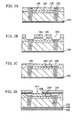
- FIGS. 1A through 1D are cross-sectional views showing process steps in a method of fabricating a semiconductor device according to an embodiment of the present invention, in which the process steps between the beginning and the collector-opening formation step are illustrated.
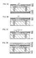
- FIGS. 2A through 2D are cross-sectional views showing process steps in the method of fabricating a semiconductor device according to the embodiment of the present invention, in which the process steps between the base-layer epitaxial growth step and the fourth-silicon-oxide-film formation step are illustrated.
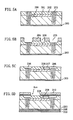
- FIGS. 3A through 3C are cross-sectional views showing process steps in the method of fabricating a semiconductor device according to the embodiment of the present invention, in which the process steps between the emitter-opening formation step and the step of doping into an emitter layer are illustrated.
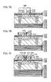
- FIGS. 4A through 4C are cross-sectional views showing process steps in the method of fabricating a semiconductor device according to the embodiment of the present invention, in which the process steps between the emitter-connecting-electrode formation step and the wiring formation step are illustrated.
- FIGS. 5A through 5D are cross-sectional views showing process steps in a conventional method of fabricating a semiconductor device, in which the process steps between the beginning and the collector-opening formation step are illustrated.
- FIGS. 6A through 6D are cross-sectional views showing process steps in the conventional method of fabricating a semiconductor device, in which the process steps between the base-layer epitaxial growth step and the fourth-silicon-oxide-film formation step are illustrated.
- FIGS. 7A through 7C are cross-sectional views showing process steps in the conventional method of fabricating a semiconductor device, in which the process steps between the emitter-opening formation step and the step of doping into an emitter layer are illustrated.
- FIGS. 8A and 8B are cross-sectional views showing process steps in the conventional method of fabricating a semiconductor device, in which the process steps between the emitter-connecting-electrode formation step and the wiring formation step are illustrated.
- FIGS. 1A through 4C are cross-sectional views showing process steps in a method of fabricating a semiconductor device according to an embodiment of the present invention.
- a p-type semiconductor substrate 100 is prepared which is made of single crystal silicon whose principal plane is the (100) plane having a resistivity of 10 to 15 ⁇ ⁇ cm, for example.
- the semiconductor substrate 100 is subjected to ion implantation using a resist film (not shown) as an implantation mask, and thus an n-type buried layer 101 is formed in a bipolar-transistor formation region of the semiconductor substrate 100 .
- a silicon crystal layer is epitaxially grown to form an n-type epitaxial layer 102 on the main surface side of the substrate.
- trenches deeper than the buried layer 101 are formed in regions located at the main surface side of the semiconductor substrate 100 and alongside of the buried layer 101 .
- thermal oxidation the surface of the deep trench is oxidized.
- a polysilicon film 103 is then deposited over all surfaces of the substrate. The resulting polysilicon film 103 is etched back, thereby providing the deep trenches filled with the polysilicon film 103 .
- a resist film 104 having shallow-trench formation regions opened therein is formed, and the semiconductor substrate 100 is etched using this resist film as an etching mask As a result, shallow trenches 105 are formed to the main surface side of the semiconductor substrate 100 .
- a first silicon oxide film 106 is deposited to the main surface side of the substrate, after which planarization of the deposited film is performed by CMP or the like. As a result, all the shallow trenches 105 are filled with the first silicon oxide film 106.
- An N-type dopant is then implanted into the contact portion of the substrate with a metallic collector electrode to form a collector connecting layer 107.
- a second silicon oxide film 108 is deposited over all surfaces of the substrate, and then a first polysilicon film 109 is deposited on the second silicon oxide film 108. Then, a resist film 110 having an opening therein is formed to the main surface side of the substrate.
- the second silicon oxide film 108 and the first polysilicon film 109 are patterned by etching using this resist film as a mask, thereby forming a collector opening Aco. In the opening Aco, a base formation region of the bipolar transistor exists.
- a p-type intrinsic base layer 111 containing a SiGe layer and a Si layer on the base formation region.
- p-type polycrystalline Si/SiGe films 112 are also formed to the main and back surface sides of the substrate.
- the first polysilicon film 109 is not necessarily required for this selective epitaxial growth of the intrinsic base layer 111.
- the intrinsic base layer 111 is grown to have a great thickness, the growth selectivity would break down, resulting in the growth of the polycrystalline Si/SiGe film 112 on the silicon oxide film as well. This undesirable growth may lead to the occurrence of particles causing the failure of semiconductor elements.
- the first polysilicon film 109 as a seed layer for the polycrystalline Si/SiGe film 112 is formed in advance.
- a characteristic of the method for fabricating a semiconductor device according to the present embodiment is to remove, immediately after the step shown in FIG. 2A , the p-type Si/SiGe film 112 which contains a contaminant and which is formed on the first polysilicon film 109 provided to the back surface side of the semiconductor substrate 100. This removal is performed by backside wet etching.
- HF hydrofluoric acid
- HNO 3 nitric acid
- a silicon nitride film may be employed in the step of defining an active region of a bipolar transistor, and the employed silicon nitride film may further be employed as an etch stopper in the wet etching step.
- the dummy run step means that the deposition of a dummy film or the heat treatment for a substrate is performed in the state in which no wafer or a dummy wafer (a dummy substrate) is placed inside the tube or chamber in the semiconductor fabrication equipment.
- a resist film 114 is formed to the main surface side of the substrate, and etching is made using this resist film as a mask such that the third silicon oxide film 113 is allowed to remain on the center portion of the intrinsic base layer 111 and on the Si/SiGe film 112.
- a p-type polysilicon film 115 is deposited over all surfaces of the substrate, after which a fourth silicon oxide film 116 is deposited on the polysilicon film 115 .
- a resist film 117 is formed to the main surface side of the substrate.
- the polysilicon film 115 and the fourth silicon oxide film 116 are patterned.
- an emitter opening Aem is formed and the center portion of the third silicon oxide film 113 is exposed at the bottom of the emitter opening Aem .
- a fifth silicon oxide film 118 is deposited over all surfaces of the substrate, and then an n-type polysilicon film 119, for example, is formed on the fifth silicon oxide film 118.
- the fifth silicon oxide film 118 and the polysilicon film 119 are etched back.
- the resulting fifth silicon oxide film 118 and polysilicon film 119 are allowed to remain as side walls on the sides of the emitter opening Aem.
- an n-type polysilicon film 120 is formed over all surfaces of the substrate, and then the substrate is subjected to heat treatment by rapid thermal annealing (RTA) or the like.
- RTA rapid thermal annealing
- the heat treatment diffuses the n-type dopant contained in the polysilicon film 120 into the intrinsic base layer 111, thereby forming an emitter layer 121.
- a resist film 122 is formed to the main surface side of the substrate.
- the polysilicon film 120, the fifth silicon oxide film 118 and the fourth silicon oxide film 116 are patterned, and the resulting polysilicon film 120 is used for an emitter connecting electrode.
- the resist film 122 is removed, after which another resist film 123 is formed to the main surface side of the substrate.
- the polysilicon film 115, the Si/SiGe film 112 and the first polysilicon film 109 are simultaneously patterned, and the resulting first polysilicon film 109, Si/SiGe film 112, and polysilicon film 115 are used for a base connecting electrode. That is to say, just before the interconnection step having a relatively high acceptable level of contamination, the polysilicon film 115, the Si/SiGe film 112 containing the contaminant and the polysilicon film 109 are dry-etched at a time.
- a sixth silicon oxide film 124 as an interlayer insulating film is deposited to the main surface side of the substrate, and then the surface of the sixth silicon oxide film 124 is planarized by chemical-mechanical polishing (CMP) or the like.
- CMP chemical-mechanical polishing
- Contact holes are then formed in portions of the sixth silicon oxide film 124 by photolithography and etching.
- an AI alloy film is deposited by sputtering in the contact holes and on the sixth silicon oxide film 124, after which the sputtered Al alloy film is patterned by photolithography and etching, thereby forming Al wiring 125 including plugs.
- a semiconductor device including a heterojunction bipolar transistor is obtained.
- a CMOS device may be formed on the semiconductor substrate 100 apart from the bipolar transistor.
- the Si/SiGe film 112 which contains the contaminant and which is formed on the first polysilicon film 109 provided to the back surface side of the semiconductor substrate 100 is removed by backside wet etching.
- the dummy run step is carried out immediately after the third silicon oxide film 113 is formed in the step shown in FIG. 2B. This makes it possible to prevent secondary contamination caused by the contaminant occurring from the intrinsic base layer 111 or the Si/SiGe film 112 through the furnace.
- a monitoring wafer used in the dummy run step is checked by elemental analysis to determine whether the wafer is contaminated or not, and the analyzed result is used as an index of process control.
- contamination can be managed with higher reliability.
- the analyzed data is stored for every type of device or every process condition. Through the use of these items of data, variation in device performance can be reduced and production yield can be improved.
- a TEOS film is deposited at the same time both on a monitoring wafer and on an 8-inch silicon wafer on all surfaces of which a SiGe film with a germanium content of 15% is grown.
- the resulting monitoring wafer is used as a first sample.
- a dummy run is carried out and then a TEOS film is deposited again on a second monitoring wafer.
- the resulting second monitoring wafer is used as a second sample.
- the TEOS film on the sample surface was dissolved and elemental analysis was conducted by an inductive coupled plasma mass spectrometry system.
- germanium with a density of 2 ⁇ 10 12 atoms/cm 2 was detected on the surface thereof.
- no germanium was detected. It was found from the result of the second sample that the second sample contained germanium at only 1 ⁇ 10 9 atoms/cm 2 or less, which is the sensitivity limit of the inductive coupled plasma spectrometry system having a quadrupol mass spectrometer.
- the dummy run step can prevent germanium contamination.
- a subsequent wafer to be processed in this equipment is not processed until a dummy run of this equipment is completed.
- a TEOS film is deposited by CVD at a higher temperature (about 680°C) than the temperature of the epitaxial growth of a SiGe film (about 550 to 600°C)
- germanium in the SiGe film is easy to diffuse outward during the CVD. Therefore, the furnace of the LP-CVD equipment used has an increased possibility of contamination. Consequently, the dummy run step is preferably carried out after the growth of a SiGe film and before the deposition of an oxide film such as a TEOS film or a nitride film.
- the recovery of the equipment means the condition that when the monitoring wafer processed in that equipment is analyzed by an inductive coupled plasma spectrometry system having a quadrupol mass spectrometer, the density of germanium contained in the wafer is less than 1 ⁇ 10 9 atoms/cm 2 , which is the sensitivity limit of the system, in other words, no germanium is detected for the analysis by the system.
- an inductive coupled plasma mass spectrometry system having a double-focusing mass spectrometer is preferably employed. This is because the double-focusing mass spectrometry has a high resolution and therefore it is less sensitive to spectral interference resulting from a matrix.
- an acid recovery solution such as hydrofluoric acid or a mixed solution of hydrofluoric acid and nitric acid can be used to dissolve the surface of a deposited film or a semiconductor substrate.
- determination about the effect of the dummy run is preferably made by using the solubility and the diffusion constant of a contaminant as indices.
- a monitoring wafer used in the dummy run step is preferably placed at the upper, center and lower points of a tube in order to check the entire tube for contamination.
- a monitoring wafer, together with semiconductor substrates which contain the contaminant and which interpose the monitoring wafer therebetween, may be placed in the tube. From this monitoring wafer, the amount of contamination can be measured.
- the analysis result of the monitoring wafer may be used as a source for determining whether or not a subsequent wafer to be processed, such as a CMOS device, can be processed in the equipment of interest.
- the polysilicon film 115, the Si/SiGe film 112 containing the contaminant and the first polysilicon film 109 are simultaneously dry-etched.
- a film as contains a contaminant is etched just before the interconnection process causing a relatively high level of contamination damage, so that secondary contamination in the master process can be prevented.
- the p-type Si/SiGe film 112 containing the contaminant is etched immediately before the silicide process not causing a lower level of contamination damage, so that secondary contamination in the master process can be prevented.
- the method for fabricating a semiconductor device according to the present embodiment is very effective in fabricating a silicon-based heterostructure device mainly made of silicon in a silicon-device fabrication line for fabricating a CMOS logic device including an MIS transistor and the like.
- heterojunction bipolar transistor in particular an NPN transistor, as an example.
- the present invention is also applicable to a PNP transistor or a heterojunction MIS transistor.
- the present invention is also applicable to a device embedded therein with a heterojunction bipolar transistor and a SiMIS transistor, and to a device embedded with a heterojunction bipolar transistor and a MIS transistor having a Si/SiGe heterojunction.
- a p-type intrinsic base may be made of Si.
- a semiconductor device including a SiGeC base layer or a SiC base layer, instead of the SiGe base layer, can also exert the effects of the present invention. That is to say, the present invention is applicable to all semiconductor devices including a Si 1-x-y Ge x C y layer (0 ⁇ x ⁇ 1, 0 ⁇ y ⁇ 1, x + y > 0).
- a semiconductor substrate having an epitaxial layer which has already contained a contaminant for a bipolar transistor, the layer is used as a collector layer
- a semiconductor substrate having an epitaxial layer which has already contained a contaminant (for a bipolar transistor, the layer is used as a collector layer) may be employed as a semiconductor substrate.
- the n-type epitaxial layer 102 is formed by in-situ doping involving a relatively high fabrication cost.
- the in-situ doping may be replaced with a high energy implantation after the epitaxial growth. This makes it possible to reduce the fabrication cost in the epitaxial growth step.
- the insulating film made up of a silicon oxide film may be replaced with that made up of a silicon nitride film.
- the deep trench is filled with the polysilicon film 103 after the surface of the deep trench is oxidized.
- the deep trench may be filled with a silicon oxide film instead of the polysilicon film 103 .
- CMP is used to planarize the sixth silicon oxide film 124 as an interlayer insulating film.
- etch back may be employed for planarization.
- a fluid interlayer insulating film (such as a BPSG film) is deposited and then the film is subjected to the reflow step by heat treatment for planarization. Planarization is not necessarily performed.
- the entire wiring in a broad sense including the plugs is formed of an Al alloy.
- W plugs and Al wiring in a narrow sense may be used together.
- Wiring and plugs may also be formed of a metal other than Al, such as Ti or Cu, or an alloy of Ti or Cu.
- thermal oxidization can be replaced with CVD in the step of forming an oxide film
- dry etching can be replaced with wet etching in the etching step, and vice versa.
Landscapes
- Bipolar Transistors (AREA)
- Testing Or Measuring Of Semiconductors Or The Like (AREA)
- Weting (AREA)
Applications Claiming Priority (3)
| Application Number | Priority Date | Filing Date | Title |
|---|---|---|---|
| JP2002099163 | 2002-04-01 | ||
| JP2002099163A JP2003297848A (ja) | 2002-04-01 | 2002-04-01 | 半導体装置の製造方法 |
| EP03007306A EP1351282A3 (de) | 2002-04-01 | 2003-03-31 | Verfahren zur Verhinderung der Kontamination während der Herstellung einer Halbleitervorrichtung |
Related Parent Applications (2)
| Application Number | Title | Priority Date | Filing Date |
|---|---|---|---|
| EP03007306.8 Division | 2003-03-31 | ||
| EP03007306A Division EP1351282A3 (de) | 2002-04-01 | 2003-03-31 | Verfahren zur Verhinderung der Kontamination während der Herstellung einer Halbleitervorrichtung |
Publications (3)
| Publication Number | Publication Date |
|---|---|
| EP1605076A2 true EP1605076A2 (de) | 2005-12-14 |
| EP1605076A3 EP1605076A3 (de) | 2006-12-13 |
| EP1605076A9 EP1605076A9 (de) | 2007-02-21 |
Family
ID=28035900
Family Applications (2)
| Application Number | Title | Priority Date | Filing Date |
|---|---|---|---|
| EP05018537A Withdrawn EP1605076A3 (de) | 2002-04-01 | 2003-03-31 | Verfahren zur Verhinderung der Kontamination während der Herstellung einer Halbleitervorrichtung |
| EP03007306A Withdrawn EP1351282A3 (de) | 2002-04-01 | 2003-03-31 | Verfahren zur Verhinderung der Kontamination während der Herstellung einer Halbleitervorrichtung |
Family Applications After (1)
| Application Number | Title | Priority Date | Filing Date |
|---|---|---|---|
| EP03007306A Withdrawn EP1351282A3 (de) | 2002-04-01 | 2003-03-31 | Verfahren zur Verhinderung der Kontamination während der Herstellung einer Halbleitervorrichtung |
Country Status (5)
| Country | Link |
|---|---|
| US (1) | US7109095B2 (de) |
| EP (2) | EP1605076A3 (de) |
| JP (1) | JP2003297848A (de) |
| CN (1) | CN1315164C (de) |
| TW (1) | TWI272651B (de) |
Families Citing this family (9)
| Publication number | Priority date | Publication date | Assignee | Title |
|---|---|---|---|---|
| WO1999024422A1 (en) | 1997-11-05 | 1999-05-20 | Neurosearch A/S | Azaring-ether derivatives and their use as nicotinic ach receptor modulators |
| US7679130B2 (en) * | 2005-05-10 | 2010-03-16 | Infineon Technologies Ag | Deep trench isolation structures and methods of formation thereof |
| US7459367B2 (en) | 2005-07-27 | 2008-12-02 | International Business Machines Corporation | Method of forming a vertical P-N junction device |
| CN100361281C (zh) * | 2005-11-11 | 2008-01-09 | 中国电子科技集团公司第五十五研究所 | 半导体平台工艺 |
| US8685176B2 (en) * | 2006-10-16 | 2014-04-01 | Ecoservices, Llc | System and method for optimized gas turbine compressor cleaning and performance measurement |
| CN101960573A (zh) * | 2008-03-04 | 2011-01-26 | HVVi半导体股份有限公司 | 硅锗碳半导体结构 |
| CN102455591A (zh) * | 2010-10-14 | 2012-05-16 | 京东方科技集团股份有限公司 | 薄膜图案和阵列基板的制造方法 |
| CN103035689B (zh) * | 2012-05-23 | 2015-06-03 | 上海华虹宏力半导体制造有限公司 | 锗硅hbt的集电区引出结构及其制造方法 |
| TWI747778B (zh) * | 2021-04-07 | 2021-11-21 | 世界先進積體電路股份有限公司 | 半導體裝置 |
Family Cites Families (17)
| Publication number | Priority date | Publication date | Assignee | Title |
|---|---|---|---|---|
| JPH05335216A (ja) * | 1992-05-29 | 1993-12-17 | Fujitsu Ltd | X線マスク及びその製造方法 |
| US5389799A (en) * | 1992-06-12 | 1995-02-14 | Kabushiki Kaisha Toshiba | Semiconductor device |
| JP2980497B2 (ja) * | 1993-11-15 | 1999-11-22 | 株式会社東芝 | 誘電体分離型バイポーラトランジスタの製造方法 |
| JP2606141B2 (ja) | 1994-06-16 | 1997-04-30 | 日本電気株式会社 | 半導体装置およびその製造方法 |
| JP3261948B2 (ja) | 1995-03-28 | 2002-03-04 | キヤノン株式会社 | X線露光用マスク及びそれを用いた半導体素子の製造方法 |
| JPH0992602A (ja) * | 1995-09-26 | 1997-04-04 | Canon Inc | マスク構造体及びその製造方法 |
| KR970054343A (ko) * | 1995-12-20 | 1997-07-31 | 이준 | 규소/규소게르마늄 쌍극자 트랜지스터 제조방법 |
| US5705830A (en) * | 1996-09-05 | 1998-01-06 | Northrop Grumman Corporation | Static induction transistors |
| US5809103A (en) * | 1996-12-20 | 1998-09-15 | Massachusetts Institute Of Technology | X-ray lithography masking |
| US5882424A (en) | 1997-01-21 | 1999-03-16 | Applied Materials, Inc. | Plasma cleaning of a CVD or etch reactor using a low or mixed frequency excitation field |
| CA2258080C (en) * | 1997-04-11 | 2007-06-05 | Nichia Chemical Industries, Ltd. | Nitride semiconductor growth method, nitride semiconductor substrate, and nitride semiconductor device |
| WO1999035311A1 (en) * | 1998-01-09 | 1999-07-15 | Asm America, Inc. | In situ growth of oxide and silicon layers |
| JP3196719B2 (ja) | 1998-03-31 | 2001-08-06 | 日本電気株式会社 | 汚染防御用隔離ラインを有する半導体製造ライン、ウエハ搬送機構および半導体の製造方法 |
| JP2001100395A (ja) * | 1999-09-30 | 2001-04-13 | Toshiba Corp | 露光用マスク及びその製造方法 |
| EP1094523A3 (de) * | 1999-10-21 | 2003-06-11 | Matsushita Electric Industrial Co., Ltd. | Lateraler Heteroübergangstransistor und Verfahren zur Herstellung |
| WO2002097864A2 (en) | 2001-05-30 | 2002-12-05 | Asm America, Inc | Low temperature load and bake |
| US6566158B2 (en) * | 2001-08-17 | 2003-05-20 | Rosemount Aerospace Inc. | Method of preparing a semiconductor using ion implantation in a SiC layer |
-
2002
- 2002-04-01 JP JP2002099163A patent/JP2003297848A/ja active Pending
-
2003
- 2003-03-13 CN CNB031204023A patent/CN1315164C/zh not_active Expired - Lifetime
- 2003-03-26 US US10/396,505 patent/US7109095B2/en not_active Expired - Lifetime
- 2003-03-28 TW TW092107111A patent/TWI272651B/zh not_active IP Right Cessation
- 2003-03-31 EP EP05018537A patent/EP1605076A3/de not_active Withdrawn
- 2003-03-31 EP EP03007306A patent/EP1351282A3/de not_active Withdrawn
Also Published As
| Publication number | Publication date |
|---|---|
| EP1351282A3 (de) | 2004-07-28 |
| TWI272651B (en) | 2007-02-01 |
| EP1605076A3 (de) | 2006-12-13 |
| EP1605076A9 (de) | 2007-02-21 |
| JP2003297848A (ja) | 2003-10-17 |
| CN1315164C (zh) | 2007-05-09 |
| US7109095B2 (en) | 2006-09-19 |
| US20030186516A1 (en) | 2003-10-02 |
| TW200401332A (en) | 2004-01-16 |
| CN1449001A (zh) | 2003-10-15 |
| EP1351282A2 (de) | 2003-10-08 |
Similar Documents
| Publication | Publication Date | Title |
|---|---|---|
| US12132096B2 (en) | Semiconductor device structure with metal gate stack | |
| US10256235B2 (en) | Vertical transistors and methods of forming same | |
| US11616064B2 (en) | Semiconductor structure | |
| US10867799B2 (en) | FinFET device and methods of forming same | |
| US12334389B2 (en) | Manufacturing method of semiconductor device | |
| US7109095B2 (en) | Method for fabricating semiconductor device | |
| US20240379862A1 (en) | Semiconductor device structure with embedded epitaxial structure | |
| US11183580B2 (en) | Structure and formation method of semiconductor device with metal gate stack | |
| US11217584B2 (en) | Limiting lateral epitaxy growth at N-P boundary using inner spacer, and related structure | |
| US11855167B2 (en) | Structure and formation method of semiconductor device with nanosheet structure | |
| US20250366162A1 (en) | Semiconductor device and methods of formation | |
| US12349374B2 (en) | Lateral bipolar transistors | |
| US20250267905A1 (en) | Semiconductor device and methods of formation | |
| US12154969B2 (en) | Semiconductor device structure with metal gate stack | |
| US20250029869A1 (en) | Isolation structure having different liners on upper and lower portions | |
| US20250364239A1 (en) | Structure and Formation Method of Semiconductor Device with Backside Conductive Contact | |
| US11757018B2 (en) | Formation method of semiconductor device with gate all around structure | |
| WO2026015209A1 (en) | Self-aligned bottom dielectric isolation for backside power delivery |
Legal Events
| Date | Code | Title | Description |
|---|---|---|---|
| PUAI | Public reference made under article 153(3) epc to a published international application that has entered the european phase |
Free format text: ORIGINAL CODE: 0009012 |
|
| AC | Divisional application: reference to earlier application |
Ref document number: 1351282 Country of ref document: EP Kind code of ref document: P |
|
| AK | Designated contracting states |
Kind code of ref document: A2 Designated state(s): AT BE BG CH CY CZ DE DK EE ES FI FR GB GR HU IE IT LI LU MC NL PT RO SE SI SK TR |
|
| AX | Request for extension of the european patent |
Extension state: AL LT LV MK |
|
| RIN1 | Information on inventor provided before grant (corrected) |
Inventor name: AOKI, SHIGETAKA Inventor name: ASAI, AKIRA Inventor name: OHNISHI, TERUHITO Inventor name: NOTAKE, HIDENORI |
|
| PUAL | Search report despatched |
Free format text: ORIGINAL CODE: 0009013 |
|
| AK | Designated contracting states |
Kind code of ref document: A3 Designated state(s): AT BE BG CH CY CZ DE DK EE ES FI FR GB GR HU IE IT LI LU MC NL PT RO SE SI SK TR |
|
| AX | Request for extension of the european patent |
Extension state: AL LT LV MK |
|
| RIC1 | Information provided on ipc code assigned before grant |
Ipc: C23C 16/44 20060101ALI20061103BHEP Ipc: H01L 21/205 20060101ALI20061103BHEP Ipc: H01L 21/20 20060101ALI20061103BHEP Ipc: H01L 21/306 20060101AFI20061103BHEP |
|
| RAP1 | Party data changed (applicant data changed or rights of an application transferred) |
Owner name: MATSUSHITA ELECTRIC INDUSTRIAL CO., LTD. |
|
| AKX | Designation fees paid |
Designated state(s): DE FR GB NL |
|
| STAA | Information on the status of an ep patent application or granted ep patent |
Free format text: STATUS: THE APPLICATION IS DEEMED TO BE WITHDRAWN |
|
| 18D | Application deemed to be withdrawn |
Effective date: 20070614 |