EP1599766B1 - Herstellungsverfahren einer mems einrichtung - Google Patents
Herstellungsverfahren einer mems einrichtung Download PDFInfo
- Publication number
- EP1599766B1 EP1599766B1 EP04717655.7A EP04717655A EP1599766B1 EP 1599766 B1 EP1599766 B1 EP 1599766B1 EP 04717655 A EP04717655 A EP 04717655A EP 1599766 B1 EP1599766 B1 EP 1599766B1
- Authority
- EP
- European Patent Office
- Prior art keywords
- comb
- fingers
- actuator
- driving element
- wheel
- Prior art date
- Legal status (The legal status is an assumption and is not a legal conclusion. Google has not performed a legal analysis and makes no representation as to the accuracy of the status listed.)
- Expired - Lifetime
Links
- 238000000034 method Methods 0.000 title claims description 22
- 210000001520 comb Anatomy 0.000 claims description 42
- 238000005530 etching Methods 0.000 claims description 18
- 239000000463 material Substances 0.000 claims description 7
- 239000004065 semiconductor Substances 0.000 claims description 7
- 230000000737 periodic effect Effects 0.000 claims description 6
- 230000009471 action Effects 0.000 claims description 5
- 230000001360 synchronised effect Effects 0.000 claims description 4
- 230000008569 process Effects 0.000 claims description 2
- 238000001338 self-assembly Methods 0.000 claims 1
- 238000004519 manufacturing process Methods 0.000 description 14
- 239000000758 substrate Substances 0.000 description 14
- 238000006073 displacement reaction Methods 0.000 description 9
- 239000011347 resin Substances 0.000 description 8
- 229920005989 resin Polymers 0.000 description 8
- VYPSYNLAJGMNEJ-UHFFFAOYSA-N Silicium dioxide Chemical compound O=[Si]=O VYPSYNLAJGMNEJ-UHFFFAOYSA-N 0.000 description 7
- XUIMIQQOPSSXEZ-UHFFFAOYSA-N Silicon Chemical compound [Si] XUIMIQQOPSSXEZ-UHFFFAOYSA-N 0.000 description 7
- 229910052710 silicon Inorganic materials 0.000 description 7
- 239000010703 silicon Substances 0.000 description 7
- 229910052814 silicon oxide Inorganic materials 0.000 description 7
- 210000000720 eyelash Anatomy 0.000 description 6
- 229910021420 polycrystalline silicon Inorganic materials 0.000 description 6
- 229920005591 polysilicon Polymers 0.000 description 4
- 239000000725 suspension Substances 0.000 description 4
- 238000005516 engineering process Methods 0.000 description 3
- 230000007246 mechanism Effects 0.000 description 3
- KRHYYFGTRYWZRS-UHFFFAOYSA-N Fluorane Chemical compound F KRHYYFGTRYWZRS-UHFFFAOYSA-N 0.000 description 2
- 230000008901 benefit Effects 0.000 description 2
- 239000003990 capacitor Substances 0.000 description 2
- 239000000470 constituent Substances 0.000 description 2
- 230000008878 coupling Effects 0.000 description 2
- 238000010168 coupling process Methods 0.000 description 2
- 238000005859 coupling reaction Methods 0.000 description 2
- 238000000151 deposition Methods 0.000 description 2
- 230000005684 electric field Effects 0.000 description 2
- 238000005265 energy consumption Methods 0.000 description 2
- 150000004767 nitrides Chemical class 0.000 description 2
- 230000009467 reduction Effects 0.000 description 2
- 239000002904 solvent Substances 0.000 description 2
- 241000256247 Spodoptera exigua Species 0.000 description 1
- 230000004888 barrier function Effects 0.000 description 1
- 239000003638 chemical reducing agent Substances 0.000 description 1
- 125000004122 cyclic group Chemical group 0.000 description 1
- 230000008021 deposition Effects 0.000 description 1
- 238000009434 installation Methods 0.000 description 1
- 239000012212 insulator Substances 0.000 description 1
- 238000003754 machining Methods 0.000 description 1
- 229910021421 monocrystalline silicon Inorganic materials 0.000 description 1
- 230000003071 parasitic effect Effects 0.000 description 1
- 230000010363 phase shift Effects 0.000 description 1
- 238000000206 photolithography Methods 0.000 description 1
- 238000001020 plasma etching Methods 0.000 description 1
- 230000002441 reversible effect Effects 0.000 description 1
Images


Classifications
-
- H—ELECTRICITY
- H02—GENERATION; CONVERSION OR DISTRIBUTION OF ELECTRIC POWER
- H02N—ELECTRIC MACHINES NOT OTHERWISE PROVIDED FOR
- H02N1/00—Electrostatic generators or motors using a solid moving electrostatic charge carrier
- H02N1/002—Electrostatic motors
- H02N1/006—Electrostatic motors of the gap-closing type
- H02N1/008—Laterally driven motors, e.g. of the comb-drive type
-
- G—PHYSICS
- G04—HOROLOGY
- G04C—ELECTROMECHANICAL CLOCKS OR WATCHES
- G04C3/00—Electromechanical clocks or watches independent of other time-pieces and in which the movement is maintained by electric means
- G04C3/08—Electromechanical clocks or watches independent of other time-pieces and in which the movement is maintained by electric means wherein movement is regulated by a mechanical oscillator other than a pendulum or balance, e.g. by a tuning fork, e.g. electrostatically
- G04C3/12—Electromechanical clocks or watches independent of other time-pieces and in which the movement is maintained by electric means wherein movement is regulated by a mechanical oscillator other than a pendulum or balance, e.g. by a tuning fork, e.g. electrostatically driven by piezoelectric means; driven by magneto-strictive means
Definitions
- the invention relates to the field of electromechanical microsystems (MEMS), and more particularly, micromotors and microreductors obtained by deep etching in a substrate of semiconductor material.
- MEMS electromechanical microsystems
- the document US 5,631,514 (published May 20, 1997) describes a micromotor adapted to rotate a gear.
- the micromotor comprises a toothed output element meshing with the toothed wheel, a connecting rod element connected to the output element and electrostatic actuators with interdigitated combs (called "comb drive” according to the English terminology generally used) controlling the displacement. of the connecting rod element.
- comb drive interdigitated combs
- the various constituent elements of the micromotor described in this document extend in different planes of the substrate. Therefore, the manufacture of the micromotor requires the etching of a substrate formed of a stack of thin layers and the use of several successive etching masks. The manufacture of the micromotor by means of surface mirco-machining of polycrystalline silicon is therefore relatively complex.
- WO 01/09519 discloses a MEMS microvalve comprising a shutter member driven in rotation by electrostatic actuators of the comb drive type.
- the electrostatic actuators act on the friction shutter element.
- micromechanism described in this document does not allow precise control of the positioning or speed of the actuated element.
- the devices described in the documents US 5,631,514 and WO 01/09519 are obtained by surface microgravure, that is to say on thin layers of silicon having a thickness of less than 4 .mu.m. Because of their small thickness, the constituent elements of these devices can not withstand significant deformations.
- the device structures proposed in these documents are therefore not suitable for driving elements with a large drive pitch (greater than or equal to 10 ⁇ m), which makes it impossible to envisage the coupling of these devices. training with conventional wheels in fields such as watchmaking.
- the structure of the actuator proposed in this document is not suitable for driving toothed elements having a pitch greater than or equal to 10 ⁇ m. Thus, this actuator does not allow to consider the coupling of the drive device with conventional wheels.
- An object of the invention is to provide a simplified method of forming an actuating mechanism of very small size and having a greater pitch than the devices of the prior art.
- the invention provides the method defined in claim 1.
- self-assembled in the context of the present invention a system free from any handling and / or assembly operation in the manufacture of the product.
- the actuator of the device of the invention implements tangential electrostatic forces exerted between the fingers of the fixed and mobile combs.
- interdigitated combs are moved relative to each other in a direction parallel to the fingers of the combs.
- the etching performed is a deep etching (etching thickness greater than 10 ⁇ m).
- the various elements of the device have sufficient thicknesses not to induce parasitic displacements (buckling) when they are stressed.
- the production of elements having lateral dimensions that is to say the dimensions in the plane of movement of the different elements
- the thickness of the elements corresponding to the thickness engraving
- the movement of the driven member is generated by a drive member which is moved in a hysteresis movement.
- the driven member is moved in a stepwise motion with a pitch greater than 10 ⁇ m.
- This device can thus be advantageously used as a clock device.
- This device does not require any reduction or reduction system.
- the drive element is therefore less bulky than conventional devices.
- All the elements of the device is formed using MEMS technology, by etching in a block of semiconductor material.
- the device thus forms an integrated component whose functions are performed in a single engraving operation.
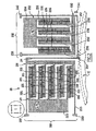
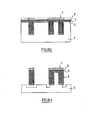
- the device comprises a toothed circular wheel 10 can be rotated by three drive actuators 20, 30, 40 distributed around the wheel and forming between them angles of 120 degrees.
- the device of the figure 1 has the particularity of being an integrated device.
- the components of the device are formed simultaneously by etching in a single block of semiconductor material.
- the engraved block portion has a thickness greater than 10 microns.
- the ungraded block portion supporting all the elements constitutes the substrate.
- the figure 2 further represents one of the drive actuators 20 of the figure 1 .
- the drive actuator 20 consists mainly of an elementary radial actuation module 201, an elementary tangential actuating module 202 and a drive element in the form of a tooth 250.
- the drive tooth 250 has a triangular shape. It extends near the wheel 10 with the tip directed towards the wheel, in a radial direction relative thereto. The drive tooth 250 is thus able to mesh with the teeth of the wheel 10.
- the expression “radial” qualifies any element extending in a radial direction relative to the wheel 10 and the expression “tangential” qualifies any element extending in a direction tangential to the wheel. , the radial and tangential directions being considered at the point of the wheel where the drive tooth is located.
- the drive tooth 250 is connected by a radial rod 211 to the radial actuation module and by a tangential rod 212 to the tangential actuating module.
- the radial actuating modules 201 and tangential 202 are electrostatic modules having a comb structure (known by the English name of "comb drive"). This type of structure includes pairs of interdigitated combs.
- the radial actuation modules 201 and tangential 202 of the structure of the actuator 20 will be described more precisely.
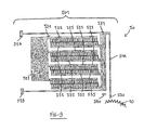
- the radial actuating module 201 is formed of a fixed part 221 and a movable part 231 to which the radial rod 211 is connected.
- the fixed portion 221 comprises a radial electrode 223 from which a set of parallel fixed combs 225 extend in a tangential direction.
- Each comb 225 is formed of a main stem and a series of parallel fingers or eyelashes connected to the rod and extending perpendicularly thereto.
- the movable portion 231 comprises a movable frame 233 having a generally U-shaped and extending around the fixed portion 221.
- the movable frame 233 is connected at each of its ends to the substrate by means of recess connections 237, 239 constituting suspensions elastic.
- Combs 235 extend from the movable frame 233 in a generally radial direction. These combs 235 are formed of a main stem and a series of parallel fingers or eyelashes connected to the rod and extending perpendicular thereto.
- the combs 225 of the fixed part 221 and the combs 235 of the movable part 231 are arranged parallel to each other and interposed with each other.
- each mobile comb 235 is arranged opposite a fixed comb 225 so that their fingers are interposed between each other, thus forming a pair of interdigitated combs.
- the tangential actuating module 202 has a structure similar to that of the radial actuating module 201, except that it is oriented perpendicular to the latter. It is formed of a fixed part 222 and a movable part 232 to which is connected the tangential rod 211.
- the fixed portion 222 comprises a tangential electrode 224 from which extend in a radial direction a set of parallel fixed combs 226.
- the movable portion 232 comprises a movable frame 232 connected at each of its ends to the substrate by means of recess connections 238, 240 constituting elastic suspensions.
- Combs 236 extend from the movable frame 232 in a tangential general direction.
- each mobile comb 236 of the movable part 232 is arranged parallel to each other and interposed with each other.
- each mobile comb 236 is arranged opposite a fixed comb 226 so that their fingers are interposed between each other, thus forming a pair of interdigitated combs.
- interposed fingers interdigitated combs are similar to planar capacitors, one of the plates is connected to the electrode 223 or 222 and the other armature is connected to the ground via the recess connections 237, 239 or 238, 240.
- the tangential electrostatic force exerted between the comb fingers causes deformation of the frame 233 and consequently the translation of the drive tooth 250 by action of the rod 211 in a radial direction with respect to the wheel 10.
- the frame 233 allows moving movable combs 235 only in the direction of the fingers.
- the same phenomenon occurs when a voltage is applied to the electrode 224.
- the electrostatic force created causes the deformation of the frame 232 and the translation of the drive tooth 250 by action of the rod 212 in a direction tangential to the wheel 10.
- the frame 232 allows a movement of the movable combs 236 only in the direction of the fingers.
- the tangential actuating module 202 comprises a stop 260 making it possible to limit the amplitude of the movement of the movable frame in order to keep the moving part 232 at a distance from the fixed part 222 and to prevent the mobile combs 236 from coming into contact with the fixed combs 226. Indeed, the contacting of the combs would generate an excessive normal electrostatic force between the combs and could lead to the collapse of the device.
- the displacement of the frame of the radial actuating module 201 is limited by the presence of the toothed wheel 10 which limits the movement of the drive tooth 250 in the radial direction.
- each of the rods allows the deformation thereof under the action of the other rod.
- the two radial and tangential flexible rods 211 and 212 provide a mechanical decoupling of the two actuating modules 201 and 202.
- the flexibility of the rods allows movement of the driving tooth independently according to two elementary degrees of freedom, namely : following the two directions of radial and tangential translation.
- the decoupling of the actuating modules 201 and 202 makes it possible to arrange them in a parallel configuration.
- the parallel configuration of the two actuating modules 201 and 202 improves the accessibility of the electrodes 223 and 224 for the installation of supply connectors.
- the Figures 3A to 3D illustrate the successive steps of operation of the actuator 20, for generating a cyclic hysteresis movement of the drive tooth 250.
- the elementary radial actuating module 201 and the elementary tangential actuating module 202 are at rest.
- the drive tooth 250 is disposed between teeth 12 and 13 of the toothed wheel 10.
- the tangential actuating module 202 is controlled so as to exert on the drive tooth 250 a tangential force via the tangential rod 212.
- the tooth 250 is then moved tangentially to the wheel 10, in the clockwise direction (as indicated by the arrow).
- the rod 211 is deformed.
- the drive tooth 250 meshes with the tooth 13 of the wheel 10 and drives it in rotation.
- the radial actuating module 201 is controlled so as to exert on the driving tooth a radial force via the radial rod 211.
- the driving tooth 250 is moved away from the wheel 10 ( as indicated by the arrow) so that it no longer meshes with it. The tooth 250 is then disengaged.
- the tangential actuating module 202 is at rest.
- the tooth 250 is then moved tangentially to the wheel 10 in the counterclockwise direction (as indicated by the arrow) to be positioned in front of the teeth 11 and 12.
- the stage of figure 3A is then renewed.
- the radial actuating module 201 and the tangential actuating module 202 are again at rest.
- the drive tooth 250 is then moved towards the wheel and disposed between the teeth 11 and 12 thereof.
- the hysteresis movement of the drive tooth 250 alternates the training phases ( Figures 3A and 3B ) and disengagement ( Figures 3C and 3D ).
- This movement allows the drive tooth 250 to mesh with the successive teeth of the wheel 10 and to drive the wheel 10 in a rotational movement stepwise clockwise.
- the wheel 10 is rotated, and this by excursions of the drive element of reduced amplitude (of the order of a micrometer).
- the figure 4 represents the hysteresis movement impressed on the tooth 250 relative to the wheel during a cycle.
- FIG. 5A to 5D represent the positions A, B, C and D taken by the drive tooth 250 relative to the teeth of the wheel.
- This FIG. also illustrates the elementary advance ⁇ of the wheel 10 generated by a cycle of displacement of the tooth 250.
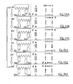
- the Figures 6A to 6D represent the addressing signals applied to the electrodes 224 and 223 of the tangential actuating modules 202 and radial 201. These signals are periodic square-wave signals, the control signal of the electrode 223 being out of phase by a quarter of a period. relative to the control signal of the electrode 224.
- the frequency of the addressing signals depends on the pitch ⁇ of the toothed wheel 10 and its diameter. Considering for example that the wheel 10 is linked to the seconds hand (second hand), the addressing frequency of the actuating modules is of the order of 10 Hz. The addressing frequencies will be divided by 60 and 720 respectively for minute and hour hands.
- the actuating modules 201 and 202 may be controlled by other types of periodic signals having a phase shift relative to each other strictly between 0 and a half period.
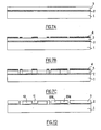
- a block is formed by depositing on a layer 1 of silicon substrate having a thickness of the order of 360 microns, a layer 2 of silicon oxide having a thickness of about 2 microns and then a layer 3 of silicon having a thickness of thickness of the order of 50 to 100 microns.
- a layer of resin 4 is deposited on the block in a pattern delimiting the various elements of the clock device.
- This layer 4 of resin forms a mask for protecting certain parts of the block.
- the resin is conventionally deposited by a photolithography technique for projecting planar geometrical shapes with a precision of the order of one micrometer.
- the parts of the block not protected by the mask are etched to the oxide layer of silicon 2 which constitutes a stop layer.
- the oxide layer of silicon 2 which constitutes a stop layer.
- different etching techniques exist.
- the block may for example be exposed to ionic bombardment (Reactive Ion Etching) which dissolves the silicon layer.
- the resin layer 4 is then removed by applying a solvent.
- the silicon oxide layer 2 is dissolved by a solution of hydrofluoric acid.
- the dissolved zones release the moving parts of the mechanism (wheel, mobile combs, rods).
- the wheel 10 is completely released from the substrate layer 1. It is held in its housing by a fixed central hub 11 constituting its axis of rotation.
- the clock device can also be manufactured using a HARPSS (High Aspect Ratio combined Poly and Single-Crystal Silicon) technique.
- HARPSS High Aspect Ratio combined Poly and Single-Crystal Silicon
- a block consisting of a layer 1 of silicon or wafer is covered with a layer of resin 4 in a pattern determining the shapes of the internal structure of the different elements of the future clock device.
- a second step represented in Figure 8B unprotected parts of the block are etched.
- a constraint to the use of HARPSS technology is that the patterns must have the same width everywhere to ensure a constant engraving depth over the entire surface of the wafer (about 50 to 100 microns).
- the resin layer 4 is then removed by applying a solvent.
- the wafer is covered with a silicon oxide layer 2 of about 1 micron thick.
- This layer of silicon oxide covers the vertical walls of the etched patterns and constitutes a barrier layer.
- a layer of nitride of 0.5 microns is deposited on the silicon oxide layer 2 thickness to isolate the future elements of the clock device of the substrate and also from each other.
- a first deposit of polysilicon 6 is made on the nitride layer 5, this first deposit being intended to cover the vertical walls of the etched patterns.
- a second polysilicon deposit 6 is made to fill the spaces formed by the etched patterns and to complete the vertical structure.
- Deposition of the polysilicon in two steps ensures complete doping of the polysilicon layer over the entire height of the etched patterns.
- a seventh step represented in figure 8G , the wafer is covered with a resin layer 7 in a pattern defining the different elements of the clock device.
- the parts of the block not protected by the resin mask 7 are etched.
- the vertical layer of silicon oxide 2 constitutes stop walls which limit the etching action. This silicon oxide layer also makes it possible to engrave the wafer under the vertical structures so as to detach the moving parts of the mechanism (wheel, mobile combs, rods).
- the present invention can find many applications, for example in the form of a chronometer engine.
- the present invention allows a supply of high frequency actuators. It therefore allows rotation at a speed of several thousand revolutions per minute.
- the present invention is particularly suitable for producing the devices previously described by means of a collective process derived from integrated circuit technology, which means that several hundred clocks are simultaneously etched in the same block of semiconductor material. .
- the present invention makes it possible to greatly simplify conventional drive trains by replacing gear trains. or conventional auxiliary speed reducers by a single toothed wheel 10, integral with the needle to be driven.
- the actuating device 20 proposed has the advantage of being reversible. In the clockwise direction of the driven element, the tangential electrostatic forces acting between the teeth of the interdigitated combs are driving. In the anti-clockwise rotation direction, it is the elastic return forces exerted notably on the moving frames that are driving.
- the actuating device proposed is in direct connection with the driven element and has a low energy consumption.
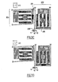
- the figure 9 represents an indexing actuator 50 that can be used in combination with a drive actuator.
- the indexing actuator 50 consists of a single radial actuating module 501 and a driving element in the form of a tooth 550.
- the radial actuating module 501 is similar to the actuating module radial 201 of the drive actuator 20.
- the radial actuating module 501 is formed of a fixed part 521 and a movable part 531 to which is connected a radial rod 511.
- the fixed part 521 comprises a radial electrode 523 from which extend in a tangential direction a set of parallel fixed combs 525.
- Each comb 525 is formed of a main stem and a series of parallel fingers or eyelashes connected to the rod and extending perpendicularly thereto.
- the movable portion 531 comprises a movable frame 533 having a generally U-shaped and extending around the fixed portion 521.
- the movable frame 533 is connected at each of its ends to the substrate by means of recess connections 537, 539 constituting suspensions elastic.
- Combs 535 extend from the movable frame 533 in a generally radial direction. These combs 535 are formed of a main stem and a series of parallel fingers or eyelashes connected to the rod and extending perpendicularly thereto.
- the combs 525 of the fixed part 521 and the combs 535 of the movable part 531 are arranged parallel to each other and inserted between them. with each other.
- each mobile comb 535 is arranged facing a fixed comb 525 so that their fingers are interposed between each other, thus forming a pair of interdigitated combs.
- the drive tooth 550 has a triangular shape. It extends near the wheel 10 with the tip directed towards the wheel, in a radial direction relative thereto. The drive tooth 550 is thus able to mesh with the teeth of the wheel 10.
- the indexing actuator 50 further comprises a stop 560 for keeping the movable portion 531 away from the fixed portion 521 to prevent the movable combs 535 from coming into contact with the fixed combs 525.
- the figure 10 schematically represents the positions taken by the drive teeth 250 and indexing 550 when the device is in operation.
- the indexing module 501 of the indexing actuator 50 is controlled in synchronism with the elementary radial actuating modules 201 and tangential 202 of the drive actuator.
- the indexing actuator has the function of keeping the wheel 10 in position when the tooth 250 of the drive actuator is disengaged (in the positions C and D). The conjunction of the drive actuator and the indexing actuator allows precise control of the positioning of the wheel 10.
- FIGS 11A to 11F represent the positions A, B, C and D taken by the drive tooth 250 and the positions E and F taken by the indexing tooth 550 relative to the teeth of the wheel 10 during a cycle of the tooth of 250
- This figure also illustrates the elementary advance ⁇ of the wheel 10 generated by a cycle of displacement of the tooth 250.
- the indexing actuator 50 is controlled to move the tooth 550 reciprocating radially relative to the wheel 10.
- the movement of the tooth 550 is synchronized with that of the tooth 250.
- the indexing tooth 550 is disengaged (in position F).
- the indexing tooth 550 is inserted between teeth of the wheel 10 (in position E) to hold the wheel in its position.
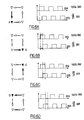
- the Figures 12A to 12F represent the addressing signals applied to the electrodes 224 and 223 of the tangential actuating modules 202 and radial 201 of the drive actuator 20 and the electrode 523 of the indexing module 501. These signals are periodic signals in niche.
- the control signal of the electrode 223 is phase shifted by a quarter of a period with respect to the control signal of the electrode 224.
- the drive tooth 250 of the drive actuator 20 is in the engaged position (position A) when no signal is applied to the electrodes 224 and 223. This allows that when the device is not energized , indexing of the wheel is provided by the tooth 250 and also generates a lower energy consumption.
- the characteristic that the tooth 250 is in the engaged position (position A) when the actuator 20 is at rest is directly related to the manufacturing process of the self-assembled device.
- the etching pattern applied to the block of semiconductor material comprises the tooth 250 in the position intermeshed between two teeth of the wheel 10.
- incompressible games appear between engraved elements.
- a game j exists for example between the toothed wheel 10 and its hub.
- This game is of the order of 4 microns.
- the pitch P of the teeth of the wheel 10 is not sufficient, the clearance j may cause uncertainty regarding the positioning of the wheel. Therefore, the pitch of the wheel is chosen to avoid such uncertainty.
- the pitch P is preferably greater than 10 microns.
- the tangential (meshing distance) and radial (clearance distance) displacement amplitudes are chosen sufficiently high.
- the engagement and disengagement distances x and y are greater than 10 ⁇ m.
Landscapes
- Physics & Mathematics (AREA)
- General Physics & Mathematics (AREA)
- Micromachines (AREA)
Claims (15)
- Verfahren zum Herstellen einer selbstorganisierten Vorrichtung, wobei das Verfahren einen Schritt zum Ätzen in einem Block aus Halbleitermaterial umfasst und wobei das Ätzen in einer Dicke ausgeführt wird, die über 10 µm liegt, und dies derart, dass eine Vorrichtung ausgebildet wird, die die folgenden Elemente umfasst:- ein angetriebenes gezahntes Element (10),- ein Antriebselement (250), das dafür eingerichtet ist, sequenziell mit dem angetriebenen gezahnten Element (10) ineinanderzugreifen,- einen Aktor (20), der dafür eingerichtet ist, das Antriebselement (250) gemäß einer Hysteresebewegung derart zu verschieben, dass das Antriebselement (250) mit aufeinanderfolgenden Zähnen (11, 12, 13) des angetriebenen Elements (10) ineinandergreift,wobei der Aktor (20) ein Antriebsmodul (201, 202) umfasst, das wenigstens einen feststehenden Kamm (225, 226) und einen beweglichen Kamm (235, 236) umfasst, wobei jeder Kamm eine Reihe von Zähnen umfasst und wobei der bewegliche Kamm (235, 236) dem feststehenden Kamm (225, 226) gegenüberstehend angeordnet ist, und dies derart, dass Zähne des feststehenden Kamms und Zähne des beweglichen Kamms ineinander geschoben sind,
wobei der bewegliche Kamm (235, 236) dafür eingerichtet ist, relativ zum feststehenden Kamm (225, 226) verschoben zu werden, und dies in einer Richtung parallel zu den Zähnen der Kämme und bei Anwendung eines Potentialunterschieds zwischen dem feststehenden Kamm und dem beweglichen Kamm, um das Antriebselement (250) in einer entsprechenden Richtung zu verschieben. - Verfahren nach Anspruch 1, bei dem der Aktor ein erstes Antriebsmodul (201) umfasst, das dafür eingerichtet ist, das Antriebselement (250) in einer ersten Richtung zu verschieben, und ein zweites Antriebsmodul (202) umfasst, das dafür eingerichtet ist, das Antriebselement (250) in einer zweiten Richtung zu verschieben, wobei die Antriebsmodule (201, 202) dafür eingerichtet sind, gleichzeitig gesteuert zu werden, um eine kombinierte Hysteresebewegung des Antriebselements (250) zu erzeugen.
- Verfahren nach Anspruch 2, bei dem das erste Antriebsmodul (201) dafür eingerichtet ist, das Antriebselement (250) in einer radialen Richtung relativ zum angetriebenen Element (10) zu verschieben, und das zweite Antriebsmodul (202) dafür eingerichtet ist, das Antriebselement (250) in einer tangentialen Richtung relativ zum angetriebenen Element (10) zu verschieben.
- Verfahren nach einem der Ansprüche 2 oder 3, bei dem das Antriebselement (250) über eine radiale biegsame Stange (211) mit dem radialen Antriebsmodul (201) und über eine tangentiale biegsame Stange (212) mit dem tangentialen Antriebsmodul (202) verbunden ist, wobei unter der Einwirkung des einen oder des anderen von den Antriebsmodulen (201, 202) die biegsamen Stangen (211, 212) das unabhängige Verschieben des Antriebselements (250) gestatten.
- Verfahren nach einem der Ansprüche 2 bis 4, bei dem die Antriebsmodule (201, 202) durch periodische Signale gesteuert werden, die gegeneinander eine Phasenverschiebung aufweisen, die streng' zwischen 0 und einer halben Periode liegt.
- Verfahren nach Anspruch 5, bei dem die periodischen Signale eine Phasenverschiebung von einer viertel Periode gegeneinander aufweisen.
- Verfahren nach einem der vorhergehenden Ansprüche, bei dem die Vorrichtung derart geätzt wird, dass das Antriebselement (250) sich in einer Eingriffsposition mit dem angetriebenen gezahnten Element (10) befindet, wenn auf den Aktor (20) kein Signal angewendet wird.
- Verfahren nach einem der vorhergehenden Ansprüche, bei dem die Vorrichtung außerdem Folgendes umfasst:- ein Positionierungselement (550), das dafür eingerichtet ist, sequenziell mit dem angetriebenen gezahnten Element (10) ineinanderzugreifen,- einen Aktor (50), der dafür eingerichtet ist, das Positionierungselement (550) entsprechend einer Bewegung zu verschieben, die mit der Hysteresebewegung des Antriebselements (250) synchronisiert ist, und dies derart, dass das Positionierungselement (550) mit Zähnen des angetriebenen Elements (10) ineinandergreift, wenn das Antriebselement (250) nicht mit Zähnen des angetriebenen Elements ineinandergreift, um das angetriebene Element (10) in Position zu halten.
- Verfahren nach Anspruch 8, bei dem der Aktor (50) ein Antriebsmodul (501) umfasst, das wenigstens einen feststehenden Kamm (525) und einen beweglichen Kamm (535) umfasst, wobei jeder Kamm eine Reihe von Zähnen umfasst und wobei der bewegliche Kamm (535) dem feststehenden Kamm (525) gegenüberstehend angeordnet ist, und dies derart, dass Zähne des feststehenden Kamms und Zähne des beweglichen Kamms ineinander geschoben sind, wobei der bewegliche Kamm (535) dafür eingerichtet ist, relativ zum feststehenden Kamm (525) verschoben zu werden, und dies in einer Richtung parallel zu den Zähnen der Kämme und bei Anwendung eines Potentialunterschieds zwischen dem feststehenden Kamm und dem beweglichen Kamm, um das Positionierungselement (550) in einer entsprechenden Richtung zu verschieben.
- Verfahren nach Anspruch 9, bei dem das Positionierungsmodul (501) durch periodische Signale gesteuert wird, die mit Steuerungssignalen für den Antriebsaktor (20) synchronisiert sind.
- Verfahren nach einem der vorhergehenden Ansprüche, bei dem die Vorrichtung durch eine SOI-Ätztechnik erhalten wird.
- Verfahren nach einem der Ansprüche 1 bis 10, bei dem die Vorrichtung durch eine HARPSS-Ätztechnik erhalten wird.
- Verfahren nach einem der vorhergehenden Ansprüche, bei dem die Vorrichtung durch ein Sammelverfahren erhalten wird, das darin besteht, gleichzeitig eine große Zahl elementarer Uhrenvorrichtungen in einen Block aus Halbleitermaterial zu ätzen.
- Verfahren nach einem der vorhergehenden Ansprüche, bei dem das angetriebene Element (10) ein Zahnrad ist.
- Verfahren nach Anspruch 14, bei dem das Rad (10) direkt fest mit einem anzutreibenden Zeiger verbunden ist.
Applications Claiming Priority (3)
| Application Number | Priority Date | Filing Date | Title |
|---|---|---|---|
| FR0302697 | 2003-03-05 | ||
| FR0302697A FR2852111B1 (fr) | 2003-03-05 | 2003-03-05 | Dispositif d'horloge utilisant la technologie mems |
| PCT/FR2004/000525 WO2004081695A2 (fr) | 2003-03-05 | 2004-03-05 | Dispositif mems comprenant un actionneur apte a generer un mouvement d’entrainement a hysteresis. |
Publications (2)
| Publication Number | Publication Date |
|---|---|
| EP1599766A2 EP1599766A2 (de) | 2005-11-30 |
| EP1599766B1 true EP1599766B1 (de) | 2013-05-08 |
Family
ID=32865257
Family Applications (1)
| Application Number | Title | Priority Date | Filing Date |
|---|---|---|---|
| EP04717655.7A Expired - Lifetime EP1599766B1 (de) | 2003-03-05 | 2004-03-05 | Herstellungsverfahren einer mems einrichtung |
Country Status (5)
| Country | Link |
|---|---|
| US (1) | US7592737B2 (de) |
| EP (1) | EP1599766B1 (de) |
| JP (1) | JP4597963B2 (de) |
| FR (1) | FR2852111B1 (de) |
| WO (1) | WO2004081695A2 (de) |
Families Citing this family (20)
| Publication number | Priority date | Publication date | Assignee | Title |
|---|---|---|---|---|
| FR2874907B1 (fr) | 2004-09-03 | 2006-11-24 | Silmach Soc Par Actions Simpli | Dispositif d'entrainement, notamment pour mecanisme horloger |
| FR2883276B1 (fr) * | 2005-03-18 | 2007-05-11 | Silmach Soc Par Actions Simpli | Procede et dispositif pour deplacer un element a entrainer utilisant un element actionneur forme par gravure dans un materiau semi-conducteur |
| FR2883277B1 (fr) * | 2005-03-18 | 2007-05-11 | Silmach Soc Par Actions Simpli | Procede et dispositif pour deplacer un element a entrainer utilisant un element actionneur forme par gravure dans un materiau semi-conducteur |
| ATE448511T1 (de) * | 2005-09-06 | 2009-11-15 | Eta Sa Mft Horlogere Suisse | Uhr mit einem halbleitenden zifferblatt |
| EP1780612A1 (de) | 2005-10-25 | 2007-05-02 | ETA SA Manufacture Horlogère Suisse | Analogic display device including a planet gear drive |
| US8915158B2 (en) * | 2006-06-02 | 2014-12-23 | MicroZeus, LLC | Methods and systems for micro transmissions |
| ATE495481T1 (de) | 2006-11-13 | 2011-01-15 | Eta Sa Mft Horlogere Suisse | Mems-mikromotor und mit diesem mikromotor ausgerüstete uhr |
| EP1921520B1 (de) | 2006-11-13 | 2009-01-28 | ETA SA Manufacture Horlogère Suisse | Einen MEMS-Mikromotor umfassendes Antriebsmodul, Verfahren zur Herstellung dieses Moduls und mit diesem Modul ausgerüstete Uhr |
| EP1921522B1 (de) * | 2006-11-13 | 2010-07-21 | ETA SA Manufacture Horlogère Suisse | Anordnung zur mechanischen Verbindung eines MEMS-Mikromotors mit einem Uhrrädchen und diese Anordnung umfassende Uhr |
| EP2060534A1 (de) * | 2007-11-16 | 2009-05-20 | Nivarox-FAR S.A. | Mikromechanisches Bauteil aus Silizium-Metall-Verbundmaterial und Verfahren zu dessen Herstellung |
| EP2164163B1 (de) * | 2008-09-16 | 2017-06-21 | ETA SA Manufacture Horlogère Suisse | Elektrostatischer Motor, der ein Stellglied umfasst |
| EP2177960B1 (de) * | 2008-10-16 | 2011-12-21 | ETA SA Manufacture Horlogère Suisse | Blockiermechanismus für Modul eines Uhrwerksantriebs |
| US8947797B2 (en) | 2010-11-15 | 2015-02-03 | DigitalOptics Corporation MEMS | Miniature MEMS actuator assemblies |
| US8803256B2 (en) | 2010-11-15 | 2014-08-12 | DigitalOptics Corporation MEMS | Linearly deployed actuators |
| EP2735922A1 (de) * | 2012-11-23 | 2014-05-28 | ETA SA Manufacture Horlogère Suisse | Zeigerantriebsmechanismus einer elektromechanischen Armbanduhr, der mit einer Verriegelung ausgestattet ist |
| FR2998737B1 (fr) * | 2012-11-26 | 2015-01-02 | Silmach | Dispositif d'actionnement avec element d'entrainement actionne par reptation |
| US8926465B2 (en) | 2013-01-07 | 2015-01-06 | Timex Group Usa, Inc. | Bidirectional MEMS driving arrangement |
| US10838366B2 (en) | 2017-09-14 | 2020-11-17 | Timex Group Usa, Inc. | Bidirectional MEMS driving arrangements with a force absorbing system |
| DE102020201241B4 (de) | 2020-01-31 | 2022-04-21 | Fraunhofer-Gesellschaft zur Förderung der angewandten Forschung eingetragener Verein | Mikroelektromechanischer antrieb zum bewegen von objekten |
| CN112966104B (zh) * | 2021-03-04 | 2022-07-12 | 网易(杭州)网络有限公司 | 文本聚类方法、装置、处理设备及存储介质 |
Family Cites Families (11)
| Publication number | Priority date | Publication date | Assignee | Title |
|---|---|---|---|---|
| US3645089A (en) * | 1969-05-28 | 1972-02-29 | Asahiro Yamada | Intermittent driving mechanism for timepiece |
| DE2216820C3 (de) * | 1971-04-07 | 1978-09-28 | Citizen Watch Co. Ltd., Tokio | Verfahren zur Einstellung der Schwingungsamplitude eines piezoelektrischen Schwingers |
| DE2216821B1 (de) | 1972-04-07 | 1973-09-27 | Siemens Ag, 1000 Berlin U. 8000 Muenchenss | Analysegerät zur Untersuchung einer Meßprobe mittels ausgelöster Auger-Elektronen |
| JPS60111178A (ja) * | 1983-11-21 | 1985-06-17 | Seiko Epson Corp | 指針表示式電子時計 |
| US4978104A (en) * | 1989-05-10 | 1990-12-18 | Gipson Jr James H | Quick release jack |
| JP2966590B2 (ja) * | 1991-07-25 | 1999-10-25 | 松下電工株式会社 | 直線駆動型圧電モータ |
| FR2700012B1 (fr) * | 1992-12-28 | 1995-03-03 | Commissariat Energie Atomique | Accéléromètre intégré à axe sensible parallèle au substrat. |
| JPH07177773A (ja) * | 1993-12-22 | 1995-07-14 | Zexel Corp | マイクロモータ |
| US5631514A (en) * | 1994-06-09 | 1997-05-20 | The United States Of America As Represented By The United States Department Of Energy | Microfabricated microengine for use as a mechanical drive and power source in the microdomain and fabrication process |
| AU6356800A (en) * | 1999-07-30 | 2001-02-19 | Procter & Gamble Company, The | Microvalve for controlling fluid flow |
| US6211599B1 (en) * | 1999-08-03 | 2001-04-03 | Sandia Corporation | Microelectromechanical ratcheting apparatus |
-
2003
- 2003-03-05 FR FR0302697A patent/FR2852111B1/fr not_active Expired - Lifetime
-
2004
- 2004-03-05 US US10/548,214 patent/US7592737B2/en not_active Expired - Lifetime
- 2004-03-05 WO PCT/FR2004/000525 patent/WO2004081695A2/fr not_active Ceased
- 2004-03-05 EP EP04717655.7A patent/EP1599766B1/de not_active Expired - Lifetime
- 2004-03-05 JP JP2006505697A patent/JP4597963B2/ja not_active Expired - Fee Related
Also Published As
| Publication number | Publication date |
|---|---|
| WO2004081695A2 (fr) | 2004-09-23 |
| WO2004081695A3 (fr) | 2004-11-18 |
| FR2852111B1 (fr) | 2005-06-24 |
| EP1599766A2 (de) | 2005-11-30 |
| FR2852111A1 (fr) | 2004-09-10 |
| US7592737B2 (en) | 2009-09-22 |
| US20070069604A1 (en) | 2007-03-29 |
| JP4597963B2 (ja) | 2010-12-15 |
| JP2006519117A (ja) | 2006-08-24 |
Similar Documents
| Publication | Publication Date | Title |
|---|---|---|
| EP1599766B1 (de) | Herstellungsverfahren einer mems einrichtung | |
| EP1835294B1 (de) | Dreiachsiger Beschleunigungsmesser mit Membran | |
| EP1797483B1 (de) | Antriebseinrichtung insbesondere für ein uhrwerk | |
| EP1390794A2 (de) | Herstellungsverfahren für einen optischen mikrospiegel und mikrospiegel oder matrixanordnung von mikrospiegeln | |
| EP2617129B1 (de) | Vorrichtung mit freihängendem träger und piezoresistive vorrichtung zur verlagerungserkennung | |
| EP3257808B1 (de) | Mikroelektromechanische und/oder nanoelektromechanische vorrichtung mit bewegung ausserhalb der ebene, die mit kapazitiven mitteln zur änderung der oberfläche ausgestattet ist | |
| EP1921521B1 (de) | MEMS-Mikromotor und mit diesem Mikromotor ausgerüstete Uhr | |
| EP2736161B1 (de) | Betätigungsvorrichtung mit durch Kriechbewegung ausgelöstem Antriebselement | |
| FR3059312A1 (fr) | Procede de realisation d’un dispositif electromecanique | |
| EP2949621B1 (de) | Kapazitive mikro- und/ oder nanoelektronische Vorrichtung mit erhöhter Kompaktheit | |
| FR2820833A1 (fr) | Micro-miroir optique a pivot, matrice de tels micro-miroirs et procede de realisation dudit micro-miroir | |
| EP1998144B1 (de) | Vorrichtung zur Übertragung einer relativen Bewegung zwischen einem zweiten und einem dritten Element eines Systems an ein erstes bewegliches Element mit Zähnen | |
| EP1921522A1 (de) | Anordnung zur mechanischen Verbindung eines MEMS-Mikromotors mit einem Uhrrädchen und diese Anordnung umfassende Uhr | |
| EP3828943B1 (de) | Mechanisches microsystem mit entsprechendem herstellungsprozess | |
| EP3264480B1 (de) | Elektromechanisches stellglied | |
| FR2865201A1 (fr) | Technique de realisation de structures a forte topologie auto-alignees | |
| EP1878108B1 (de) | Einrichtung und verfahren zur verstellung einer antrieb, mit aktuatorelement in halbleitermaterial geätzten | |
| EP1921520A1 (de) | Einen MEMS-Mikromotor umfassendes Antriebsmodul, Verfahren zur Herstellung dieses Moduls und mit diesem Modul ausgerüstete Uhr | |
| EP4194960B1 (de) | Piezoelektrische spiralfeder und verfahren zur herstellung dieser spiralfeder | |
| EP1641709A2 (de) | Verfahren zum trennen einer nützlichen schicht und durch das verfahren erhaltene komponente | |
| EP1697783A1 (de) | Optische komponenten und herstellung dafür | |
| EP1746071A1 (de) | Mikroaktuator mit Balken mit gekrümmten Segmenten |
Legal Events
| Date | Code | Title | Description |
|---|---|---|---|
| PUAI | Public reference made under article 153(3) epc to a published international application that has entered the european phase |
Free format text: ORIGINAL CODE: 0009012 |
|
| 17P | Request for examination filed |
Effective date: 20050926 |
|
| AK | Designated contracting states |
Kind code of ref document: A2 Designated state(s): AT BE BG CH CY CZ DE DK EE ES FI FR GB GR HU IE IT LI LU MC NL PL PT RO SE SI SK TR |
|
| AX | Request for extension of the european patent |
Extension state: AL LT LV MK |
|
| DAX | Request for extension of the european patent (deleted) | ||
| 17Q | First examination report despatched |
Effective date: 20100318 |
|
| GRAP | Despatch of communication of intention to grant a patent |
Free format text: ORIGINAL CODE: EPIDOSNIGR1 |
|
| GRAS | Grant fee paid |
Free format text: ORIGINAL CODE: EPIDOSNIGR3 |
|
| GRAP | Despatch of communication of intention to grant a patent |
Free format text: ORIGINAL CODE: EPIDOSNIGR1 |
|
| 111L | Licence recorded |
Designated state(s): AT BE BG CH CY CZ DE DK EE ES FI FR GB GR HU IE IT LU MC NL PL PT RO SE SI SK TR Free format text: EXCLUSIVE LICENSE Name of requester: SILMACH, FR Effective date: 20130128 |
|
| GRAA | (expected) grant |
Free format text: ORIGINAL CODE: 0009210 |
|
| 111L | Licence recorded |
Designated state(s): AT BE BG CH CY CZ DE DK EE ES FI FR GB GR HU IE IT LU MC NL PL PT RO SE SI SK TR Free format text: EXCLUSIVE LICENSE Name of requester: SILMACH, FR Effective date: 20130128 |
|
| AK | Designated contracting states |
Kind code of ref document: B1 Designated state(s): AT BE BG CH CY CZ DE DK EE ES FI FR GB GR HU IE IT LI LU MC NL PL PT RO SE SI SK TR |
|
| REG | Reference to a national code |
Ref country code: GB Ref legal event code: FG4D Free format text: NOT ENGLISH |
|
| REG | Reference to a national code |
Ref country code: CH Ref legal event code: EP Ref country code: AT Ref legal event code: REF Ref document number: 611354 Country of ref document: AT Kind code of ref document: T Effective date: 20130515 Ref country code: CH Ref legal event code: PK Free format text: COMPLETEMENT D'ENREGISTREMENT DE LICENCE: LICENCE EXCLUSIVE |
|
| REG | Reference to a national code |
Ref country code: CH Ref legal event code: NV Representative=s name: MICHELI AND CIE SA, CH |
|
| REG | Reference to a national code |
Ref country code: IE Ref legal event code: FG4D Free format text: LANGUAGE OF EP DOCUMENT: FRENCH |
|
| REG | Reference to a national code |
Ref country code: DE Ref legal event code: R096 Ref document number: 602004042040 Country of ref document: DE Effective date: 20130704 |
|
| REG | Reference to a national code |
Ref country code: AT Ref legal event code: MK05 Ref document number: 611354 Country of ref document: AT Kind code of ref document: T Effective date: 20130508 |
|
| REG | Reference to a national code |
Ref country code: NL Ref legal event code: VDEP Effective date: 20130508 |
|
| PG25 | Lapsed in a contracting state [announced via postgrant information from national office to epo] |
Ref country code: GR Free format text: LAPSE BECAUSE OF FAILURE TO SUBMIT A TRANSLATION OF THE DESCRIPTION OR TO PAY THE FEE WITHIN THE PRESCRIBED TIME-LIMIT Effective date: 20130809 Ref country code: FI Free format text: LAPSE BECAUSE OF FAILURE TO SUBMIT A TRANSLATION OF THE DESCRIPTION OR TO PAY THE FEE WITHIN THE PRESCRIBED TIME-LIMIT Effective date: 20130508 Ref country code: PT Free format text: LAPSE BECAUSE OF FAILURE TO SUBMIT A TRANSLATION OF THE DESCRIPTION OR TO PAY THE FEE WITHIN THE PRESCRIBED TIME-LIMIT Effective date: 20130909 Ref country code: ES Free format text: LAPSE BECAUSE OF FAILURE TO SUBMIT A TRANSLATION OF THE DESCRIPTION OR TO PAY THE FEE WITHIN THE PRESCRIBED TIME-LIMIT Effective date: 20130819 Ref country code: AT Free format text: LAPSE BECAUSE OF FAILURE TO SUBMIT A TRANSLATION OF THE DESCRIPTION OR TO PAY THE FEE WITHIN THE PRESCRIBED TIME-LIMIT Effective date: 20130508 Ref country code: SE Free format text: LAPSE BECAUSE OF FAILURE TO SUBMIT A TRANSLATION OF THE DESCRIPTION OR TO PAY THE FEE WITHIN THE PRESCRIBED TIME-LIMIT Effective date: 20130508 Ref country code: SI Free format text: LAPSE BECAUSE OF FAILURE TO SUBMIT A TRANSLATION OF THE DESCRIPTION OR TO PAY THE FEE WITHIN THE PRESCRIBED TIME-LIMIT Effective date: 20130508 |
|
| PG25 | Lapsed in a contracting state [announced via postgrant information from national office to epo] |
Ref country code: BG Free format text: LAPSE BECAUSE OF FAILURE TO SUBMIT A TRANSLATION OF THE DESCRIPTION OR TO PAY THE FEE WITHIN THE PRESCRIBED TIME-LIMIT Effective date: 20130808 Ref country code: CY Free format text: LAPSE BECAUSE OF FAILURE TO SUBMIT A TRANSLATION OF THE DESCRIPTION OR TO PAY THE FEE WITHIN THE PRESCRIBED TIME-LIMIT Effective date: 20130508 Ref country code: PL Free format text: LAPSE BECAUSE OF FAILURE TO SUBMIT A TRANSLATION OF THE DESCRIPTION OR TO PAY THE FEE WITHIN THE PRESCRIBED TIME-LIMIT Effective date: 20130508 |
|
| PG25 | Lapsed in a contracting state [announced via postgrant information from national office to epo] |
Ref country code: DK Free format text: LAPSE BECAUSE OF FAILURE TO SUBMIT A TRANSLATION OF THE DESCRIPTION OR TO PAY THE FEE WITHIN THE PRESCRIBED TIME-LIMIT Effective date: 20130508 Ref country code: SK Free format text: LAPSE BECAUSE OF FAILURE TO SUBMIT A TRANSLATION OF THE DESCRIPTION OR TO PAY THE FEE WITHIN THE PRESCRIBED TIME-LIMIT Effective date: 20130508 Ref country code: EE Free format text: LAPSE BECAUSE OF FAILURE TO SUBMIT A TRANSLATION OF THE DESCRIPTION OR TO PAY THE FEE WITHIN THE PRESCRIBED TIME-LIMIT Effective date: 20130508 Ref country code: CZ Free format text: LAPSE BECAUSE OF FAILURE TO SUBMIT A TRANSLATION OF THE DESCRIPTION OR TO PAY THE FEE WITHIN THE PRESCRIBED TIME-LIMIT Effective date: 20130508 |
|
| PG25 | Lapsed in a contracting state [announced via postgrant information from national office to epo] |
Ref country code: RO Free format text: LAPSE BECAUSE OF FAILURE TO SUBMIT A TRANSLATION OF THE DESCRIPTION OR TO PAY THE FEE WITHIN THE PRESCRIBED TIME-LIMIT Effective date: 20130508 Ref country code: NL Free format text: LAPSE BECAUSE OF FAILURE TO SUBMIT A TRANSLATION OF THE DESCRIPTION OR TO PAY THE FEE WITHIN THE PRESCRIBED TIME-LIMIT Effective date: 20130508 Ref country code: IT Free format text: LAPSE BECAUSE OF FAILURE TO SUBMIT A TRANSLATION OF THE DESCRIPTION OR TO PAY THE FEE WITHIN THE PRESCRIBED TIME-LIMIT Effective date: 20130508 |
|
| PLBE | No opposition filed within time limit |
Free format text: ORIGINAL CODE: 0009261 |
|
| STAA | Information on the status of an ep patent application or granted ep patent |
Free format text: STATUS: NO OPPOSITION FILED WITHIN TIME LIMIT |
|
| 26N | No opposition filed |
Effective date: 20140211 |
|
| REG | Reference to a national code |
Ref country code: DE Ref legal event code: R097 Ref document number: 602004042040 Country of ref document: DE Effective date: 20140211 |
|
| REG | Reference to a national code |
Ref country code: FR Ref legal event code: PLFP Year of fee payment: 13 |
|
| PG25 | Lapsed in a contracting state [announced via postgrant information from national office to epo] |
Ref country code: TR Free format text: LAPSE BECAUSE OF FAILURE TO SUBMIT A TRANSLATION OF THE DESCRIPTION OR TO PAY THE FEE WITHIN THE PRESCRIBED TIME-LIMIT Effective date: 20130508 Ref country code: HU Free format text: LAPSE BECAUSE OF FAILURE TO SUBMIT A TRANSLATION OF THE DESCRIPTION OR TO PAY THE FEE WITHIN THE PRESCRIBED TIME-LIMIT; INVALID AB INITIO Effective date: 20040305 |
|
| REG | Reference to a national code |
Ref country code: FR Ref legal event code: PLFP Year of fee payment: 14 |
|
| REG | Reference to a national code |
Ref country code: FR Ref legal event code: PLFP Year of fee payment: 15 |
|
| PGFP | Annual fee paid to national office [announced via postgrant information from national office to epo] |
Ref country code: IE Payment date: 20220225 Year of fee payment: 19 Ref country code: GB Payment date: 20220316 Year of fee payment: 19 Ref country code: DE Payment date: 20220307 Year of fee payment: 19 Ref country code: CH Payment date: 20220321 Year of fee payment: 19 |
|
| PGFP | Annual fee paid to national office [announced via postgrant information from national office to epo] |
Ref country code: MC Payment date: 20220221 Year of fee payment: 19 Ref country code: LU Payment date: 20220225 Year of fee payment: 19 Ref country code: FR Payment date: 20220331 Year of fee payment: 19 Ref country code: BE Payment date: 20220316 Year of fee payment: 19 |
|
| REG | Reference to a national code |
Ref country code: DE Ref legal event code: R119 Ref document number: 602004042040 Country of ref document: DE |
|
| PG25 | Lapsed in a contracting state [announced via postgrant information from national office to epo] |
Ref country code: MC Free format text: LAPSE BECAUSE OF NON-PAYMENT OF DUE FEES Effective date: 20230331 |
|
| REG | Reference to a national code |
Ref country code: CH Ref legal event code: PL |
|
| GBPC | Gb: european patent ceased through non-payment of renewal fee |
Effective date: 20230305 |
|
| REG | Reference to a national code |
Ref country code: BE Ref legal event code: MM Effective date: 20230331 |
|
| PG25 | Lapsed in a contracting state [announced via postgrant information from national office to epo] |
Ref country code: LU Free format text: LAPSE BECAUSE OF NON-PAYMENT OF DUE FEES Effective date: 20230305 |
|
| REG | Reference to a national code |
Ref country code: IE Ref legal event code: MM4A |
|
| PG25 | Lapsed in a contracting state [announced via postgrant information from national office to epo] |
Ref country code: GB Free format text: LAPSE BECAUSE OF NON-PAYMENT OF DUE FEES Effective date: 20230305 |
|
| PG25 | Lapsed in a contracting state [announced via postgrant information from national office to epo] |
Ref country code: LI Free format text: LAPSE BECAUSE OF NON-PAYMENT OF DUE FEES Effective date: 20230331 Ref country code: IE Free format text: LAPSE BECAUSE OF NON-PAYMENT OF DUE FEES Effective date: 20230305 Ref country code: GB Free format text: LAPSE BECAUSE OF NON-PAYMENT OF DUE FEES Effective date: 20230305 Ref country code: FR Free format text: LAPSE BECAUSE OF NON-PAYMENT OF DUE FEES Effective date: 20230331 Ref country code: DE Free format text: LAPSE BECAUSE OF NON-PAYMENT OF DUE FEES Effective date: 20231003 Ref country code: CH Free format text: LAPSE BECAUSE OF NON-PAYMENT OF DUE FEES Effective date: 20230331 |
|
| PG25 | Lapsed in a contracting state [announced via postgrant information from national office to epo] |
Ref country code: BE Free format text: LAPSE BECAUSE OF NON-PAYMENT OF DUE FEES Effective date: 20230331 |