EP1598695A2 - Terahertzwellengenerator und Terahertzwellendetektor - Google Patents
Terahertzwellengenerator und Terahertzwellendetektor Download PDFInfo
- Publication number
- EP1598695A2 EP1598695A2 EP05010742A EP05010742A EP1598695A2 EP 1598695 A2 EP1598695 A2 EP 1598695A2 EP 05010742 A EP05010742 A EP 05010742A EP 05010742 A EP05010742 A EP 05010742A EP 1598695 A2 EP1598695 A2 EP 1598695A2
- Authority
- EP
- European Patent Office
- Prior art keywords
- semiconductor crystal
- terahertz wave
- terahertz
- zincblende
- type iii
- Prior art date
- Legal status (The legal status is an assumption and is not a legal conclusion. Google has not performed a legal analysis and makes no representation as to the accuracy of the status listed.)
- Granted
Links
Images




Classifications
-
- G—PHYSICS
- G02—OPTICS
- G02F—OPTICAL DEVICES OR ARRANGEMENTS FOR THE CONTROL OF LIGHT BY MODIFICATION OF THE OPTICAL PROPERTIES OF THE MEDIA OF THE ELEMENTS INVOLVED THEREIN; NON-LINEAR OPTICS; FREQUENCY-CHANGING OF LIGHT; OPTICAL LOGIC ELEMENTS; OPTICAL ANALOGUE/DIGITAL CONVERTERS
- G02F1/00—Devices or arrangements for the control of the intensity, colour, phase, polarisation or direction of light arriving from an independent light source, e.g. switching, gating or modulating; Non-linear optics
- G02F1/35—Non-linear optics
- G02F1/353—Frequency conversion, i.e. wherein a light beam is generated with frequency components different from those of the incident light beams
-
- B—PERFORMING OPERATIONS; TRANSPORTING
- B82—NANOTECHNOLOGY
- B82Y—SPECIFIC USES OR APPLICATIONS OF NANOSTRUCTURES; MEASUREMENT OR ANALYSIS OF NANOSTRUCTURES; MANUFACTURE OR TREATMENT OF NANOSTRUCTURES
- B82Y20/00—Nanooptics, e.g. quantum optics or photonic crystals
-
- G—PHYSICS
- G02—OPTICS
- G02F—OPTICAL DEVICES OR ARRANGEMENTS FOR THE CONTROL OF LIGHT BY MODIFICATION OF THE OPTICAL PROPERTIES OF THE MEDIA OF THE ELEMENTS INVOLVED THEREIN; NON-LINEAR OPTICS; FREQUENCY-CHANGING OF LIGHT; OPTICAL LOGIC ELEMENTS; OPTICAL ANALOGUE/DIGITAL CONVERTERS
- G02F1/00—Devices or arrangements for the control of the intensity, colour, phase, polarisation or direction of light arriving from an independent light source, e.g. switching, gating or modulating; Non-linear optics
- G02F1/35—Non-linear optics
- G02F1/355—Non-linear optics characterised by the materials used
- G02F1/3556—Semiconductor materials, e.g. quantum wells
-
- G—PHYSICS
- G02—OPTICS
- G02F—OPTICAL DEVICES OR ARRANGEMENTS FOR THE CONTROL OF LIGHT BY MODIFICATION OF THE OPTICAL PROPERTIES OF THE MEDIA OF THE ELEMENTS INVOLVED THEREIN; NON-LINEAR OPTICS; FREQUENCY-CHANGING OF LIGHT; OPTICAL LOGIC ELEMENTS; OPTICAL ANALOGUE/DIGITAL CONVERTERS
- G02F1/00—Devices or arrangements for the control of the intensity, colour, phase, polarisation or direction of light arriving from an independent light source, e.g. switching, gating or modulating; Non-linear optics
- G02F1/35—Non-linear optics
- G02F1/353—Frequency conversion, i.e. wherein a light beam is generated with frequency components different from those of the incident light beams
- G02F1/3544—Particular phase matching techniques
- G02F1/3548—Quasi phase matching [QPM], e.g. using a periodic domain inverted structure
-
- G—PHYSICS
- G02—OPTICS
- G02F—OPTICAL DEVICES OR ARRANGEMENTS FOR THE CONTROL OF LIGHT BY MODIFICATION OF THE OPTICAL PROPERTIES OF THE MEDIA OF THE ELEMENTS INVOLVED THEREIN; NON-LINEAR OPTICS; FREQUENCY-CHANGING OF LIGHT; OPTICAL LOGIC ELEMENTS; OPTICAL ANALOGUE/DIGITAL CONVERTERS
- G02F2203/00—Function characteristic
- G02F2203/13—Function characteristic involving THZ radiation
Definitions
- the present invention relates to semiconductor crystals for generating terahertz waves, terahertz wave generators incorporating the semiconductor crystals, semiconductor crystals for detecting terahertz waves, and terahertz wave detectors incorporating the semiconductor crystals.
- Terahertz waves are electromagnetic waves having a frequency in the range of 0.1 to 10 THz (wavelength: 30 to 3,000 ⁇ m) and their wavelength substantially overlaps infrared and far-infrared regions.
- the terahertz region ranging from 0.1 to 10 THz has not been extensively explored in the past. Recently, studies are being conducted to apply the electromagnetic waves in this region to environmental instrumentation such as imaging or tomography, biology, and medical science, and the terahertz waves are thus increasingly gaining importance. In order to expand the applications of the terahertz waves, efficient generation and detection of terahertz waves are indispensable.
- the present invention relates to semiconductor crystals for generating terahertz waves, terahertz wave generators incorporating the semiconductor crystals, methods for generating terahertz waves using the semiconductor crystals, terahertz wave detectors incorporating the semiconductor crystals, and methods for detecting terahertz waves using the semiconductor crystals.
- a difference frequency generation technique using a parametric element As the methods for generating terahertz waves, a difference frequency generation technique using a parametric element, a parametric oscillator generation technique using a nonlinear element, a generation technique using a crystal having electro-optic effects (hereinafter referred to as "EO effects"), and the like have been available.
- EO effects electro-optic effects
- the technique of generating terahertz waves by utilizing the EO effects advantageously has high practicality since the technique allows easy optical alignment.
- optically conductive antennas those that utilize electro-optical (EO) effects, such as ZnTe, etc.
- EO electro-optical
- terahertz waves are generated by pumping ZnTe with ultrashort light pulses of 0.8 ⁇ m and are detected by sampling terahertz waves incident on ZnTe with ultrashort light pulses of 0.8 ⁇ m.
- Terahertz waves can be generated and detected with ZnTe and 0.8 ⁇ m ultrashort light pulses because the interactive length that allows phase matching in ZnTe is relatively large between 0.8 ⁇ m ultrashort light pulses and terahertz wave pulses.
- the interactive length that allows phase matching is hereinafter also referred to as "coherent length”.
- ultrashort light pulses are generated by a large-scale Ti:sapphire laser system in a free space and are thus rarely applicable to optical communication fibers.
- the device that generates and detects terahertz waves is also large and requires complicated optical alignment.
- the thickness of ZnTe must be reduced to 100 ⁇ m or less to achieve phase matching.
- crystals having EO effects that can highly efficiently generate and detect terahertz waves using ultrashort light pulses in the optical communication band have not been known in the art.
- An object of the invention is to provide a crystal having EO effects that can highly efficiently generate and detect terahertz waves using ultrashort light pulses in the optical communication band.
- Terahertz wave generator incorporating the crystal, a method for generating terahertz waves using the crystal, a terahertz wave detector incorporating the crystal, and a method for detecting terahertz waves using the crystal are also provided.
- an aspect of present invention provides a terahertz wave generator including a light source for generating a pump beam which is an ultrashort light pulse in the optical communication band; and a terahertz wave-generating semiconductor crystal comprising a zincblende-type III-V compound semiconductor crystal that has a predetermined thickness and generates terahertz wave pulses upon application of the pump beam generated from the light source.
- the zincblende-type III-V compound semiconductor crystal has a large interactive length (coherent length) in which phase matching is achieved between the ultrashort light pulses in the optical communication band and the terahertz wave pulses.
- terahertz waves can be highly efficiently generated by using the ultrashort light pulses in the optical communication band as the pump beam.
- the zincblende-type III-V compound semiconductor crystal is preferably one selected from the group consisting of GaAs, InGaAs, InGaAsP, InAlAs, InP, GaP, GaSb, and AlSb crystals. These crystals are transparent in the optical communication band and thus can highly efficiently generate terahertz waves with smaller absorption loss of the pump beam.
- the zincblende-type III-V compound semiconductor crystal is preferably a quasi-phase matching crystal.
- the quasi-phase matching crystal can increase the substantial interactive length and can thus generate terahertz waves in a high bandwidth at high efficiency.
- the quasi-phase matching crystal is constituted from layers of a first semiconductor crystal (P) and a second semiconductor crystal (N) alternately stacked on each other, the first semiconductor crystal having a group index at the wavelength of the pump beam larger than the refractive index at the wavelength of the terahertz waves, the second semiconductor crystal having a group index at the wavelength of the pump beam smaller than the refractive index at the wavelength of the terahertz waves.
- Such a quasi-phase matching crystal can be easily produced by a semiconductor crystal film production technique such as metalorganic chemical vapor deposition (MOCVD), molecular beam epitaxy (MBE), or the like.
- MOCVD metalorganic chemical vapor deposition
- MBE molecular beam epitaxy
- the semiconductor crystals (P) and (N) are preferably one selected from the group consisting of GaAs, InGaAs, InGaAsP, InAlAs, InP, GaP, GaSb, and AlSb crystals. These crystals are transparent in the optical communication band and thus can highly efficiently generate terahertz waves with smaller absorption loss of the pump beam.
- the light source may be a fiber laser including an Er-or Yb-doped fiber serving as a gain medium.
- the thickness of the semiconductor crystal may be adjusted to generate to generate terahertz wave pulses of a particular wavelength. By setting the thickness to the local minimum of the coherent length curve, terahertz waves having a wavelength that satisfies that coherent length can be generated.
- a terahertz wave detector including a terahertz wave-detecting semiconductor crystal comprising a zincblende-type III-V compound semiconductor crystal that emits a modified sampling beam modified with an electrical field signal of a terahertz wave pulse upon temporal and spatial overlap irradiation with the terahertz wave pulse and an ultrashort light pulse in the optical communication band serving as a sampling beam; an irradiation unit that applies the terahertz wave pulse and the sampling beam to the zincblende-type III-V compound semiconductor crystal so that the terahertz wave pulse and the sampling beam temporary and spatially overlap each other; and an optical detector for detecting the sampling beam modified by an electrical field signal of the terahertz wave pulse and emitted from the zincblende-type III-V compound semiconductor crystal.
- the zincblende-type III-V compound semiconductor crystal has a large interactive length (coherent length) in which phase matching is achieved between the ultrashort light pulses in the optical communication band and the terahertz wave pulses.
- terahertz waves can be highly efficiently detected by using the ultrashort light pulses in the optical communication band as the sampling beam.
- the zincblende-type III-V compound semiconductor crystal is preferably one selected from the group consisting of GaAs, InGaAs, InGaAsP, InAlAs, InP, GaP, GaSb, and AlSb crystals. These crystals are transparent in the optical communication band and thus can highly efficiently detect terahertz waves with a smaller absorption loss of the sampling beam.
- the zincblende-type III-V compound semiconductor crystal is preferably a quasi-phase matching crystal.
- the quasi-phase matching crystal can increase the substantial interactive length and can thus detect terahertz waves in a high bandwidth at high efficiency.
- the quasi-phase matching crystal may be constituted from layers of a first semiconductor crystal (P') and a second semiconductor crystal (N') alternately stacked on each other, the first semiconductor crystal having a group index at the wavelength of the sampling beam greater than the refractive index at the wavelength of the terahertz waves, the second semiconductor crystal having a group index at the wavelength of the sampling beam smaller than the refractive index at the wavelength of the terahertz waves.
- Such a quasi-phase matching crystal can be easily produced by a semiconductor crystal film production technique such as metalorganic chemical vapor deposition (MOCVD), molecular beam epitaxy (MBE), or the like.
- MOCVD metalorganic chemical vapor deposition
- MBE molecular beam epitaxy
- the terahertz wave detector may further include a light source that generates the ultrashort light pulse in the optical communication band; a splitter that splits the ultrashort light pulse into a pump beam and the sampling beam, and a terahertz wave-generating semiconductor crystal comprising a zincblende-type III-V compound semiconductor crystal that has a predetermined thickness and generates the terahertz wave pulse upon irradiation with the pump beam.
- the irradiation unit applies both of the terahertz wave pulse generated from the terahertz wave-generating semiconductor crystal and the sampling beam to the terahertz wave-detecting semiconductor crystal.
- the light source may be a fiber laser including an Er-or Yb-doped fiber serving as a gain medium.
- Another aspect of the invention provides a method for generating terahertz waves at high efficiency, the method including a pump beam-generating step of generating an ultrashort light pulse in the optical communication band serving as a pump beam; and an irradiation/generation step of applying the pump beam to a zincblende-type III-V compound semiconductor crystal having a predetermined thickness to generate a terahertz wave pulse.
- the zincblende-type III-V compound semiconductor crystal is preferably a quasi-phase matching crystal and is preferably one selected from the group consisting of GaAs, InGaAs, InGaAsP, InAlAs, InP, GaP, GaSb, and AlSb crystals.
- the quasi-phase matching crystal is constituted from layers of a first semiconductor crystal (P) and a second semiconductor crystal (N) alternately stacked on each other, the first semiconductor crystal having a group index at the wavelength of the pump beam larger than the refractive index at the wavelength of the terahertz waves, the second semiconductor crystal having a group index at the wavelength of the pump beam smaller than the refractive index at the wavelength of the terahertz waves.
- the semiconductor crystals (P) and (N) are preferably one selected from the group consisting of GaAs, InGaAs, InGaAsP, InAlAs, InP, GaP, GaSb, and AlSb crystals.
- the thickness of the semiconductor crystal may be adjusted to generate to generate terahertz wave pulses of a particular wavelength.
- Yet another aspect of the present invention provides a method for highly efficiently detecting terahertz waves, the method including a step of temporal and spatial overlap irradiation of a zincblende-type III-V compound semiconductor crystal with a terahertz wave pulse and an ultrashort light pulse in the optical communication band serving as a sampling beam so that the sampling beam modified with an electrical field signal of the terahertz wave is emitted from the zincblende-type III-V compound semiconductor crystal.
- the zincblende-type III-V compound semiconductor crystal is preferably a quasi-phase matching crystal and is preferably one selected from the group consisting of GaAs, InGaAs, InGaAsP, InAlAs, InP, GaP, GaSb, and AlSb crystals.
- the quasi-phase matching crystal is constituted from layers of a first semiconductor crystal (P') and a second semiconductor crystal (N') alternately stacked on each other, the first semiconductor crystal having a group index at the wavelength of the pump beam larger than the refractive index at the wavelength of the terahertz waves, the second semiconductor crystal having a group index at the wavelength of the pump beam smaller than the refractive index at the wavelength of the terahertz waves.
- the semiconductor crystals (P') and (N') are preferably one selected from the group consisting of GaAs, InGaAs, InGaAsP, InAlAs, InP, GaP, GaSb, and AlSb crystals.
- Fig. 1 is an outline diagram showing a terahertz wave generation/detection system including an inventive high-efficiency terahertz wave generator and an inventive high-efficiency terahertz wave detector.
- Ultrashort light pulses in the optical communication band generated from a light source 1 are split into a pump beam and a sampling beam using a beam splitter 11 serving as a splitter.
- the terahertz wave generator includes the light source 1 and a zincblende-type III-V compound semiconductor crystal 2 that has a predetermined thickness and generates terahertz waves when the pump beam concentrated with a lens 14 is applied.
- the terahertz wave detector includes a zincblende-type III-V compound semiconductor crystal 3 and an overlap irradiation unit 4 that apply terahertz waves and the sampling beam to the zincblende-type III-V compound semiconductor crystal 3 so that the terahertz waves temporally and spatially overlap the sampling beam.
- An example of the light source 1 for generating ultrashort light pulses in the optical communication band is a femtosecond fiber laser including a gain medium composed of a fiber doped with a rare-earth element such as Er or Yb.
- FEMTOLITE produced by Aisin Seiki Co., Ltd. is preferable.
- the zincblende-type III-V compound semiconductor crystal 2 will be described later together with the zincblende-type III-V compound semiconductor crystal 3 of the terahertz wave detector.
- the overlap irradiation unit 4 include an optical delay line 41 for applying the sampling beam and the terahertz waves to the zincblende-type III-V compound semiconductor crystal 3 so that the terahertz waves temporally overlap the sampling beam; an off-axis parabolic mirror 42 that concentrates and collimates the terahertz waves generated from the semiconductor crystal 2; a perforated off-axis parabolic mirror 43 that concentrates the collimated terahertz waves and applies the concentrated collimated terahertz waves to the zincblende-type III-V compound semiconductor crystal 3; and a lens 44 that concentrates the sampling beam and applies the concentrated sampling beam to the zincblende-type III-V compound semiconductor crystal 3 through a hole formed in the perforated off-axis parabolic mirror 43 so that the same position of the semiconductor crystal 3 is irradiated with the terahertz waves and.the sampling beam.
- the system also includes optical path bending mirrors 12, a quarter wavelength plate 15, a Wollaston prism 16, and InGaAs optical detectors 17 and 17'.
- the zincblende-type III-V compound semiconductor crystals 2 and 3 are preferably composed of one selected from GaAs, InGaAs, InGaAsP, InAlAs, InP, GaP, GaSb, and AlSb, which is transparent in the optical communication band.
- the phase matching between the pump beam and the generated terahertz waves and the phase matching between the sampling beam and the terahertz waves to be detected must be achieved.
- the interactive length (coherent length) for phase matching must be large enough to generate and detect terahertz waves at high efficiencies.
- n 2 ps A + B ⁇ 2 ps/( ⁇ 2 ps - C 2 ) wherein parameter A is 8.950, B is 2.054, and C 2 is 0.390 ⁇ m 2 .
- n THz stabilizes at 3.6 at 3 THz or lower.
- the dispersion curve of n g shows that n g ⁇ n THz when ⁇ ps > 1.35 ⁇ m.
- the phase condition is met when ⁇ ps > 1.35 ⁇ m.
- the zincblende-type III-V compound semiconductor crystals 2 and 3 shown in Fig. 1 may be composed of GaAs when the pump beam or the sampling beam has a wavelength of 1.35 ⁇ m or more.
- Fig. 3 shows that the semiconductor crystals 2 and 3 shown in Fig. 1 may be composed of InP when the pump beam or sampling beam has a wavelength of 1.2 ⁇ m or more.
- Fig. 4 shows that the semiconductor crystals 2 and 3 shown in Fig. 1 may be composed of GaP when the pump beam or sampling beam has a wavelength of 1.0 ⁇ m or more.
- a semiconductor crystal 2 composed of GaAs 2 mm in thickness will achieve phase matching up to 0.7 THz for a 1.56 ⁇ m pump beam and up to 2.8 THz for a 1.33 ⁇ m pump beam.
- terahertz waves up to these frequencies can be respectively generated.
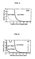
- Fig. 5 also shows that a semiconductor crystal 3 composed of GaAs 2 mm in thickness will achieve phase matching up to 0.7 THz for a 1.56 ⁇ m sampling beam and up to 2.8 THz for a 1.33 ⁇ m sampling beam. Thus, terahertz waves up to these frequencies can be respectively detected.
- Fig. 5 shows that the cutoff frequency of detectable terahertz waves when the semiconductor crystal 3 is composed of GaAs and has a thickness of 2 mm is 0.7 THz for a 1.56 ⁇ m sampling beam and is 2.8 THz for a 1.33 ⁇ m sampling beam. By changing the thickness of the semiconductor crystal, the cutoff frequency of the detectable terahertz waves can be adjusted.
- Fig. 6 shows that a semiconductor crystal 2 having a thickness of 1 mm and being composed of InP can generate terahertz waves up to 0.4 THz for a 1.04 ⁇ m pump beam, up to 0.75 THz for a 1.56 ⁇ m pump beam, and up to 3.5 THz for a 1.22 pump beam.
- a 1.22 ⁇ m pump beam a local minimum appears in the coherent length curve.
- 1.2 THz waves can be selectively generated.
- a semiconductor crystal 3 having a thickness of 1 mm and being composed of InP can detect terahertz waves up to 0.4 THz for a 1.04 ⁇ m sampling beam, up to 0.75 THz for a 1.56 ⁇ m sampling beam, and up to 3.5 THz for a 1.22 sampling beam.
- Fig. 7 shows that a semiconductor crystal 2 having a thickness of 0.5 mm and being composed of GaP can generate terahertz waves of up to 4.5 THz for a 1.04 ⁇ m pump beam and up to 5.5 THz for a 0.98 ⁇ m pump beam.
- a local minimum appears in the coherent length curve.
- a semiconductor crystal 3 having a thickness of 0.5 mm and being composed of GaP can detect terahertz waves of up to 4.5 THz for a 1.04 ⁇ m sampling beam and up to 5.5 THz for a 0.98 sampling beam.
- the semiconductor crystal 2 for generating terahertz waves and the semiconductor crystal 3 for detecting terahertz waves are preferably (110) crystals. Generation and detection can be efficiently carried out by utilizing the inversion symmetry of the nonlinear susceptibility ⁇ (2) .
- the frequency band of terahertz waves that can be generated or detected can be expanded.
- the quasi-phase matching crystals can be produced as follows.
- the regions marked by ellipses are each a region near the intersection of the group index n g curve and the leveled portion of n THz obtained by extrapolation, i.e., a region in which n g - n THz is near 0.
- Quasi-phase matching is achievable with the wavelength (indicated by the abscissa) near these regions.
- the thickness of the laminate may be adjusted to the coherent length that corresponds to the frequency region for terahertz waves to be generated and detected. Lamination may be conducted by metalorganic chemical vapor deposition (MOCVD), molecular beam epitaxy (MBE), or the like.
- MOCVD metalorganic chemical vapor deposition
- MBE molecular beam epitaxy
- An ultrashort light pulse in the optical communication band generated from the light source 1 is split into a pump beam and a sampling beam with a beam splitter 11.
- the sampling beam is reflected at two mirrors 12 for bending the optical path, concentrated by the lens 44, and is applied to the zincblende-type III-V compound semiconductor crystal 3 through the hole in the perforated off-axis parabolic mirror 43.
- the pump beam is reflected at the mirror 12 for bending the optical path, given a predetermined temporal delay at the optical delay line 41, concentrated with the lens 44, and is applied to the zincblende-type III-V compound semiconductor crystal 2.
- the semiconductor crystal 2 Once irradiated with the pump beam in the optical communication band, the semiconductor crystal 2 generates terahertz waves.
- the generated terahertz waves are collimated with the off-axis parabolic mirror 42, and concentrated and applied to the zincblende-type III-V compound semiconductor crystal 3 with the perforated off-axis parabolic mirror 43 so that the pump beam and the sampling beam are coaxial (spatial overlap).
- the predetermined time delay given by the optical delay line 41 is adjusted so that the sampling beam and the terahertz waves are simultaneously irradiates (temporal overlap) the semiconductor crystal 3.
- the semiconductor crystal 3 irradiated with terahertz waves allows the polarized light of the sampling beam passing through the crystal to rotate due to the Pockels effect caused by the electric field signal. As a result, the sampling beam becomes elliptically polarized after it passed through the quarter wavelength plate 15. Accordingly, a difference in component is generated between the p-polarized light and the s-polarized light.
- the p-polarized light and the s-polarized light are split with the Wollaston prism 16 and detected with the optical detectors 17 and 17', which output different electrical signals.
- the difference between the electrical signals is in proportion to the electrical field of the terahertz waves applied to the semiconductor crystal 3.
- the electrical field of the terahertz waves can be determined from the electrical signals output from the optical detectors 17 and 17'.
- the SN ratio of the signals can be increased by inserting an optical chopper in the light path of the terahertz waves and amplifying the electrical signals output from the optical detectors 17 and 17' with a lock-in amplifier.
- the ultrashort light pulse in the optical communication band generated from the light source 1 propagates in air.
- use of optical fibers has become popular since optical fibers can transmit light in the optical communication band at low loss.
- modifications may be made to the system shown in Fig. 1 so that the pulse is transmitted through optical fibers from the light source 1 to the lens 14 and to the lens 44.
- the optical delay line 41 may also be constituted from optical fibers. In this manner, size-reduction and stable operation can be ensured.
- EXAMPLE 1 a small fiber laser for emitting laser beams having a wavelength of 1.56 ⁇ m, a repetition frequency of 50 MHz, a pulse width of 100 fs, and an output of 380 mW was used as the light source 1 shown in Fig. 1.
- a (110) GaAs crystal having a thickness of 0.5 mm was used as the zincblende-type III-V compound semiconductor crystals 2 and 3.
- the electrical field signal waveform of the terahertz waves obtained in this example is shown in Fig. 8.
- a power spectrum of the terahertz waves obtained by Fourier transform of the electrical field signal waveform shown in Fig. 8 is shown in Fig. 9. Terahertz waves up to about 3 THz were generated and detected.
- a small fiber laser for emitting laser beams having a wavelength of 1.04 ⁇ m, a repetition frequency of 50 MHz, a pulse width of 100 fs, and an output of 380 mW was used as the light source 1 shown in Fig. 1.
- the quasi-phase matching crystal shown in Fig. 10 and the quasi-phase matching crystal shown in Fig. 11 were used as the semiconductor crystals 2 and 3, respectively.
- the quasi-phase matching crystal (the semiconductor crystal 2) shown in Fig. 10 was constituted from a total of ten alternately stacked semiconductor layers 21 and 22.
- the semiconductor layers 21 were composed of a semiconductor crystal (P) in which the difference between the group index at the pump beam wavelength and the refractive index in the terahertz region was positive, and the semiconductor layers 22 were composed of a semiconductor crystal (N) in which the difference was negative.
- Each semiconductor layer 21 was composed of InP and had a thickness of 100 ⁇ m.
- Each semiconductor layer 22 was composed of GaP and had a thickness of 100 ⁇ m.
- the quasi-phase matching crystal (the semiconductor crystal 3) shown in Fig. 11 was constituted from a total of ten alternately stacked semiconductor layers 31 and 32.
- the semiconductor layers 31 were composed of a semiconductor crystal (P') in which the difference between the group index at the pump beam wavelength and the refractive index in the terahertz region was positive, and the semiconductor layers 32 were composed of a semiconductor crystal (N') in which the difference was negative.
- Each semiconductor layer 31 was composed of InP and had a thickness of 100 ⁇ m.
- Each semiconductor layer 32 was composed of GaP and had a thickness of 100 ⁇ m.
- Fig. 12 shows the power spectrum of the terahertz waves obtained in this EXAMPLE. Terahertz waves up to about 5 THz were generated and detected.
- EXAMPLE 3 a small fiber laser for emitting laser beams having a wavelength of 1.22 ⁇ m, a repetition frequency of 50 MHz, a pulse width of 100 fs, and an output of 300 mW was used as the light source 1 shown in Fig. 1.
- An InP (110) crystal having a thickness of 8.5 mm was used as the zincblende-type III-V compound semiconductor crystal 2
- a GaAs (110) crystal having a thickness of 0.5 mm was used as the zincblende-type III-V compound semiconductor crystal 3.
- the power spectrum of the terahertz waves obtained in this example is shown in Fig. 13. Terahertz waves in a narrow band ranging from 1 to 1.6 THz were selectively generated.
- a terahertz wave-generating semiconductor crystal includes a zincblende-type III-V compound semiconductor crystal that generates terahertz wave pulses upon application of an ultrashort light pulse in the optical communication band serving as a pump beam.
Landscapes
- Physics & Mathematics (AREA)
- Nonlinear Science (AREA)
- Optics & Photonics (AREA)
- General Physics & Mathematics (AREA)
- Chemical & Material Sciences (AREA)
- Engineering & Computer Science (AREA)
- Nanotechnology (AREA)
- Life Sciences & Earth Sciences (AREA)
- Biophysics (AREA)
- Crystallography & Structural Chemistry (AREA)
- Optical Modulation, Optical Deflection, Nonlinear Optics, Optical Demodulation, Optical Logic Elements (AREA)
- Lasers (AREA)
Applications Claiming Priority (2)
| Application Number | Priority Date | Filing Date | Title |
|---|---|---|---|
| JP2004149576A JP4445325B2 (ja) | 2004-05-19 | 2004-05-19 | テラヘルツ波発生用半導体結晶、その結晶を用いたテラヘルツ波発生装置とその方法及びテラヘルツ波検出装置とその方法 |
| JP2004149576 | 2004-05-19 |
Publications (3)
| Publication Number | Publication Date |
|---|---|
| EP1598695A2 true EP1598695A2 (de) | 2005-11-23 |
| EP1598695A3 EP1598695A3 (de) | 2006-01-04 |
| EP1598695B1 EP1598695B1 (de) | 2016-06-22 |
Family
ID=34936632
Family Applications (1)
| Application Number | Title | Priority Date | Filing Date |
|---|---|---|---|
| EP05010742.4A Expired - Lifetime EP1598695B1 (de) | 2004-05-19 | 2005-05-18 | Terahertzwellengenerator und Terahertzwellendetektor |
Country Status (3)
| Country | Link |
|---|---|
| US (1) | US7177071B2 (de) |
| EP (1) | EP1598695B1 (de) |
| JP (1) | JP4445325B2 (de) |
Cited By (3)
| Publication number | Priority date | Publication date | Assignee | Title |
|---|---|---|---|---|
| US8809092B2 (en) | 2009-07-17 | 2014-08-19 | Edmund Linfield | Generating and detecting radiation |
| CN104022427A (zh) * | 2014-04-28 | 2014-09-03 | 中国科学院上海光学精密机械研究所 | 波形可控太赫兹辐射的产生装置 |
| CN107462548A (zh) * | 2017-08-21 | 2017-12-12 | 燕山大学 | 基于THz‑TDS技术的地下综合管廊气体浓度检测装置及检测方法 |
Families Citing this family (14)
| Publication number | Priority date | Publication date | Assignee | Title |
|---|---|---|---|---|
| DE102006042642B4 (de) * | 2006-09-12 | 2010-06-24 | Batop Gmbh | Terahertz Time-Domain Spektrometer |
| US7808636B2 (en) * | 2007-01-11 | 2010-10-05 | Rensselaer Polytechnic Institute | Systems, methods, and devices for handling terahertz radiation |
| EP2202481A1 (de) * | 2007-10-16 | 2010-06-30 | Aisin Seiki Kabushiki Kaisha | Nicht-kontakt-filmdickemessverfahren und einrichtung |
| JP5196436B2 (ja) * | 2008-11-11 | 2013-05-15 | アイシン精機株式会社 | テラヘルツ波発生装置及びテラヘルツ波発生方法 |
| DE102010032382A1 (de) | 2010-07-27 | 2012-02-02 | Batop Gmbh | Fasergekoppeltes Terahertz Time-Domain Spektrometer |
| US9040919B2 (en) * | 2010-10-25 | 2015-05-26 | Thomas E. Darcie | Photomixer-waveguide coupling tapers |
| US9250128B2 (en) * | 2012-03-02 | 2016-02-02 | Beihang University | Method and apparatus for optical asynchronous sampling signal measurements |
| JP5844694B2 (ja) * | 2012-06-27 | 2016-01-20 | 日本電信電話株式会社 | テラヘルツ波発生装置 |
| CN102940935B (zh) * | 2012-11-15 | 2016-01-20 | 中国科学院深圳先进技术研究院 | 太赫兹波发生装置 |
| US20150124336A1 (en) * | 2013-06-25 | 2015-05-07 | Public Service Solutions, Inc. | Wide spectrum optical systems and devices implementing first surface mirrors |
| RU2546052C1 (ru) * | 2013-11-21 | 2015-04-10 | Федеральное Государственное Бюджетное Образовательное Учреждение Высшего Профессионального Образования "Саратовский Государственный Университет Имени Н.Г. Чернышевского" | Способ получения электромагнитного излучения гига- и терагерцового диапазона частот |
| RU2637182C2 (ru) * | 2015-11-11 | 2017-11-30 | федеральное государственное автономное образовательное учреждение высшего образования "Нижегородский государственный университет им. Н.И. Лобачевского" | Рабочий узел детектора импульсного терагерцового излучения |
| JP7228792B2 (ja) * | 2019-06-07 | 2023-02-27 | パナソニックIpマネジメント株式会社 | 波長変換装置 |
| CN113363464A (zh) * | 2021-06-08 | 2021-09-07 | 广东工业大学 | 一种镓硅磷复合负极活性材料、锂离子电池及其制备方法和应用 |
Family Cites Families (7)
| Publication number | Priority date | Publication date | Assignee | Title |
|---|---|---|---|---|
| US5355247A (en) | 1993-03-30 | 1994-10-11 | The Board Of Trustees Of The Leland Stanford, Jr. University | Method using a monolithic crystalline material for producing radiation by quasi-phase-matching, diffusion bonded monolithic crystalline material for quasi-phase-matching, and method for fabricating same |
| US6414473B1 (en) * | 1996-05-31 | 2002-07-02 | Rensselaer Polytechnic Institute | Electro-optic/magneto-optic measurement of electromagnetic radiation using chirped optical pulse |
| JP3388319B2 (ja) * | 1996-05-31 | 2003-03-17 | レンセレー ポリテクニク インスティテュート | 自由空間の電磁放射を特徴づけるための電気光学及び磁気光学感知装置及び方法 |
| JP2002072269A (ja) | 2000-08-30 | 2002-03-12 | Inst Of Physical & Chemical Res | テラヘルツ波発生方法及び装置 |
| AUPR213900A0 (en) * | 2000-12-15 | 2001-01-25 | Luminis Pty Limited | A diagnostic apparatus |
| US6734974B2 (en) * | 2001-01-25 | 2004-05-11 | Rensselaer Polytechnic Institute | Terahertz imaging with dynamic aperture |
| JP2003015175A (ja) * | 2001-04-27 | 2003-01-15 | Mitsubishi Electric Corp | 固体光源装置 |
-
2004
- 2004-05-19 JP JP2004149576A patent/JP4445325B2/ja not_active Expired - Fee Related
-
2005
- 2005-05-18 EP EP05010742.4A patent/EP1598695B1/de not_active Expired - Lifetime
- 2005-05-19 US US11/132,411 patent/US7177071B2/en not_active Expired - Fee Related
Cited By (3)
| Publication number | Priority date | Publication date | Assignee | Title |
|---|---|---|---|---|
| US8809092B2 (en) | 2009-07-17 | 2014-08-19 | Edmund Linfield | Generating and detecting radiation |
| CN104022427A (zh) * | 2014-04-28 | 2014-09-03 | 中国科学院上海光学精密机械研究所 | 波形可控太赫兹辐射的产生装置 |
| CN107462548A (zh) * | 2017-08-21 | 2017-12-12 | 燕山大学 | 基于THz‑TDS技术的地下综合管廊气体浓度检测装置及检测方法 |
Also Published As
| Publication number | Publication date |
|---|---|
| US20050258368A1 (en) | 2005-11-24 |
| US7177071B2 (en) | 2007-02-13 |
| EP1598695B1 (de) | 2016-06-22 |
| JP2005332954A (ja) | 2005-12-02 |
| EP1598695A3 (de) | 2006-01-04 |
| JP4445325B2 (ja) | 2010-04-07 |
Similar Documents
| Publication | Publication Date | Title |
|---|---|---|
| US7177071B2 (en) | Semiconductor crystal for generating terahertz waves, terahertz wave-generator incorporating the crystal, semiconductor crystal for detecting terahertz waves, and terahertz waves detector incorporating the crystal | |
| Song et al. | Handbook of terahertz technologies: devices and applications | |
| US6738397B2 (en) | Solid-state light source apparatus | |
| US8415625B2 (en) | Total reflection terahertz wave measurement device | |
| CN102879971B (zh) | 一种连续调节太赫兹波中心频率和频谱宽度的方法 | |
| EP2609466B1 (de) | Vorrichtung zur erzeugung elektromagnetischer thz wellen, vorrichtung zur detektion von elektromagnetischen thz wellen, und zeitdomänenspektroskopie-apparat | |
| JP2015222414A (ja) | テラヘルツ波発生装置、及びこれを用いた測定装置 | |
| JP3598375B2 (ja) | テラヘルツ電磁波時間分解分光装置 | |
| Gale et al. | Broad-bandwidth parametric amplification in the visible: femtosecond experiments and simulations | |
| CN105790044A (zh) | 基于脉冲偏振整形的双色场光丝诱导太赫兹场增强系统 | |
| Maussang et al. | Echo-less photoconductive antenna sources for high-resolution terahertz time-domain spectroscopy | |
| Chen et al. | Continuously tunable and energy-enhanced injection pulse-seeded terahertz parametric generator based on KTP crystal | |
| Cherchi et al. | Exploiting the optical quadratic nonlinearity of zinc-blende semiconductors for guided-wave terahertz generation: a material comparison | |
| RU2386933C1 (ru) | Измеритель мощности излучения импульсных оптических квантовых генераторов | |
| JP2013080939A (ja) | 光伝導基板およびこれを用いた電磁波発生検出装置 | |
| Ganichev et al. | All-electric detection of the polarization state of terahertz laser radiation | |
| Yin et al. | Terahertz sources and detectors | |
| Du et al. | Absorption measurement of a 50-mm-long periodically poled lithium niobate optical parametric oscillator pumped at 1064 nm by a Nd: YAG laser | |
| CN115588893B (zh) | 一种倍频关系双波长太赫兹参量产生器 | |
| Ouchi et al. | Terahertz tomography system using fiber lasers and applications | |
| Gill | Non-Linear Terahertz Spectroscopy of Quantum Materials | |
| Nikoghosyan | Laser driven terahertz dielectric wedge antenna placed in free space or in hollow metallic waveguide | |
| Kondawar | Integrated terahertz quantum cascade laser system for space research | |
| Lerer et al. | Broadband generation of terahertz waves via infrared frequency nondegenerate parametric down-conversion by nonlinear graphene arrays | |
| Mosley | Terahertz Time-Domain Spectroscopy |
Legal Events
| Date | Code | Title | Description |
|---|---|---|---|
| PUAI | Public reference made under article 153(3) epc to a published international application that has entered the european phase |
Free format text: ORIGINAL CODE: 0009012 |
|
| PUAL | Search report despatched |
Free format text: ORIGINAL CODE: 0009013 |
|
| AK | Designated contracting states |
Kind code of ref document: A2 Designated state(s): AT BE BG CH CY CZ DE DK EE ES FI FR GB GR HU IE IS IT LI LT LU MC NL PL PT RO SE SI SK TR |
|
| AX | Request for extension of the european patent |
Extension state: AL BA HR LV MK YU |
|
| AK | Designated contracting states |
Kind code of ref document: A3 Designated state(s): AT BE BG CH CY CZ DE DK EE ES FI FR GB GR HU IE IS IT LI LT LU MC NL PL PT RO SE SI SK TR |
|
| AX | Request for extension of the european patent |
Extension state: AL BA HR LV MK YU |
|
| 17P | Request for examination filed |
Effective date: 20060113 |
|
| AKX | Designation fees paid |
Designated state(s): DE FR GB |
|
| GRAP | Despatch of communication of intention to grant a patent |
Free format text: ORIGINAL CODE: EPIDOSNIGR1 |
|
| INTG | Intention to grant announced |
Effective date: 20160308 |
|
| GRAS | Grant fee paid |
Free format text: ORIGINAL CODE: EPIDOSNIGR3 |
|
| GRAA | (expected) grant |
Free format text: ORIGINAL CODE: 0009210 |
|
| AK | Designated contracting states |
Kind code of ref document: B1 Designated state(s): DE FR GB |
|
| REG | Reference to a national code |
Ref country code: GB Ref legal event code: FG4D |
|
| REG | Reference to a national code |
Ref country code: DE Ref legal event code: R096 Ref document number: 602005049547 Country of ref document: DE |
|
| REG | Reference to a national code |
Ref country code: DE Ref legal event code: R097 Ref document number: 602005049547 Country of ref document: DE |
|
| PLBE | No opposition filed within time limit |
Free format text: ORIGINAL CODE: 0009261 |
|
| STAA | Information on the status of an ep patent application or granted ep patent |
Free format text: STATUS: NO OPPOSITION FILED WITHIN TIME LIMIT |
|
| 26N | No opposition filed |
Effective date: 20170323 |
|
| REG | Reference to a national code |
Ref country code: DE Ref legal event code: R119 Ref document number: 602005049547 Country of ref document: DE |
|
| GBPC | Gb: european patent ceased through non-payment of renewal fee |
Effective date: 20170518 |
|
| REG | Reference to a national code |
Ref country code: FR Ref legal event code: ST Effective date: 20180131 |
|
| PG25 | Lapsed in a contracting state [announced via postgrant information from national office to epo] |
Ref country code: GB Free format text: LAPSE BECAUSE OF NON-PAYMENT OF DUE FEES Effective date: 20170518 Ref country code: DE Free format text: LAPSE BECAUSE OF NON-PAYMENT OF DUE FEES Effective date: 20171201 |
|
| PG25 | Lapsed in a contracting state [announced via postgrant information from national office to epo] |
Ref country code: FR Free format text: LAPSE BECAUSE OF NON-PAYMENT OF DUE FEES Effective date: 20170531 |