EP1592999B1 - Pixel tft arrangement for active matrix display - Google Patents
Pixel tft arrangement for active matrix display Download PDFInfo
- Publication number
- EP1592999B1 EP1592999B1 EP04707968.6A EP04707968A EP1592999B1 EP 1592999 B1 EP1592999 B1 EP 1592999B1 EP 04707968 A EP04707968 A EP 04707968A EP 1592999 B1 EP1592999 B1 EP 1592999B1
- Authority
- EP
- European Patent Office
- Prior art keywords
- pixel
- electrodes
- level
- gate
- dielectric layer
- Prior art date
- Legal status (The legal status is an assumption and is not a legal conclusion. Google has not performed a legal analysis and makes no representation as to the accuracy of the status listed.)
- Expired - Lifetime
Links
Images




Classifications
-
- G—PHYSICS
- G02—OPTICS
- G02F—OPTICAL DEVICES OR ARRANGEMENTS FOR THE CONTROL OF LIGHT BY MODIFICATION OF THE OPTICAL PROPERTIES OF THE MEDIA OF THE ELEMENTS INVOLVED THEREIN; NON-LINEAR OPTICS; FREQUENCY-CHANGING OF LIGHT; OPTICAL LOGIC ELEMENTS; OPTICAL ANALOGUE/DIGITAL CONVERTERS
- G02F1/00—Devices or arrangements for the control of the intensity, colour, phase, polarisation or direction of light arriving from an independent light source, e.g. switching, gating or modulating; Non-linear optics
- G02F1/01—Devices or arrangements for the control of the intensity, colour, phase, polarisation or direction of light arriving from an independent light source, e.g. switching, gating or modulating; Non-linear optics for the control of the intensity, phase, polarisation or colour
- G02F1/13—Devices or arrangements for the control of the intensity, colour, phase, polarisation or direction of light arriving from an independent light source, e.g. switching, gating or modulating; Non-linear optics for the control of the intensity, phase, polarisation or colour based on liquid crystals, e.g. single liquid crystal display cells
- G02F1/133—Constructional arrangements; Operation of liquid crystal cells; Circuit arrangements
- G02F1/1333—Constructional arrangements; Manufacturing methods
- G02F1/1343—Electrodes
-
- G—PHYSICS
- G02—OPTICS
- G02B—OPTICAL ELEMENTS, SYSTEMS OR APPARATUS
- G02B5/00—Optical elements other than lenses
- G02B5/20—Filters
- G02B5/201—Filters in the form of arrays
-
- G—PHYSICS
- G02—OPTICS
- G02F—OPTICAL DEVICES OR ARRANGEMENTS FOR THE CONTROL OF LIGHT BY MODIFICATION OF THE OPTICAL PROPERTIES OF THE MEDIA OF THE ELEMENTS INVOLVED THEREIN; NON-LINEAR OPTICS; FREQUENCY-CHANGING OF LIGHT; OPTICAL LOGIC ELEMENTS; OPTICAL ANALOGUE/DIGITAL CONVERTERS
- G02F1/00—Devices or arrangements for the control of the intensity, colour, phase, polarisation or direction of light arriving from an independent light source, e.g. switching, gating or modulating; Non-linear optics
- G02F1/01—Devices or arrangements for the control of the intensity, colour, phase, polarisation or direction of light arriving from an independent light source, e.g. switching, gating or modulating; Non-linear optics for the control of the intensity, phase, polarisation or colour
- G02F1/13—Devices or arrangements for the control of the intensity, colour, phase, polarisation or direction of light arriving from an independent light source, e.g. switching, gating or modulating; Non-linear optics for the control of the intensity, phase, polarisation or colour based on liquid crystals, e.g. single liquid crystal display cells
- G02F1/133—Constructional arrangements; Operation of liquid crystal cells; Circuit arrangements
- G02F1/136—Liquid crystal cells structurally associated with a semi-conducting layer or substrate, e.g. cells forming part of an integrated circuit
-
- G—PHYSICS
- G02—OPTICS
- G02F—OPTICAL DEVICES OR ARRANGEMENTS FOR THE CONTROL OF LIGHT BY MODIFICATION OF THE OPTICAL PROPERTIES OF THE MEDIA OF THE ELEMENTS INVOLVED THEREIN; NON-LINEAR OPTICS; FREQUENCY-CHANGING OF LIGHT; OPTICAL LOGIC ELEMENTS; OPTICAL ANALOGUE/DIGITAL CONVERTERS
- G02F1/00—Devices or arrangements for the control of the intensity, colour, phase, polarisation or direction of light arriving from an independent light source, e.g. switching, gating or modulating; Non-linear optics
- G02F1/01—Devices or arrangements for the control of the intensity, colour, phase, polarisation or direction of light arriving from an independent light source, e.g. switching, gating or modulating; Non-linear optics for the control of the intensity, phase, polarisation or colour
- G02F1/13—Devices or arrangements for the control of the intensity, colour, phase, polarisation or direction of light arriving from an independent light source, e.g. switching, gating or modulating; Non-linear optics for the control of the intensity, phase, polarisation or colour based on liquid crystals, e.g. single liquid crystal display cells
- G02F1/133—Constructional arrangements; Operation of liquid crystal cells; Circuit arrangements
- G02F1/136—Liquid crystal cells structurally associated with a semi-conducting layer or substrate, e.g. cells forming part of an integrated circuit
- G02F1/1362—Active matrix addressed cells
- G02F1/136227—Through-hole connection of the pixel electrode to the active element through an insulation layer
-
- H—ELECTRICITY
- H10—SEMICONDUCTOR DEVICES; ELECTRIC SOLID-STATE DEVICES NOT OTHERWISE PROVIDED FOR
- H10D—INORGANIC ELECTRIC SEMICONDUCTOR DEVICES
- H10D86/00—Integrated devices formed in or on insulating or conducting substrates, e.g. formed in silicon-on-insulator [SOI] substrates or on stainless steel or glass substrates
- H10D86/01—Manufacture or treatment
- H10D86/021—Manufacture or treatment of multiple TFTs
- H10D86/0221—Manufacture or treatment of multiple TFTs comprising manufacture, treatment or patterning of TFT semiconductor bodies
- H10D86/0223—Manufacture or treatment of multiple TFTs comprising manufacture, treatment or patterning of TFT semiconductor bodies comprising crystallisation of amorphous, microcrystalline or polycrystalline semiconductor materials
- H10D86/0229—Manufacture or treatment of multiple TFTs comprising manufacture, treatment or patterning of TFT semiconductor bodies comprising crystallisation of amorphous, microcrystalline or polycrystalline semiconductor materials characterised by control of the annealing or irradiation parameters
-
- H—ELECTRICITY
- H10—SEMICONDUCTOR DEVICES; ELECTRIC SOLID-STATE DEVICES NOT OTHERWISE PROVIDED FOR
- H10D—INORGANIC ELECTRIC SEMICONDUCTOR DEVICES
- H10D86/00—Integrated devices formed in or on insulating or conducting substrates, e.g. formed in silicon-on-insulator [SOI] substrates or on stainless steel or glass substrates
- H10D86/01—Manufacture or treatment
- H10D86/021—Manufacture or treatment of multiple TFTs
- H10D86/0241—Manufacture or treatment of multiple TFTs using liquid deposition, e.g. printing
-
- H—ELECTRICITY
- H10—SEMICONDUCTOR DEVICES; ELECTRIC SOLID-STATE DEVICES NOT OTHERWISE PROVIDED FOR
- H10K—ORGANIC ELECTRIC SOLID-STATE DEVICES
- H10K10/00—Organic devices specially adapted for rectifying, amplifying, oscillating or switching; Organic capacitors or resistors having potential barriers
- H10K10/40—Organic transistors
- H10K10/46—Field-effect transistors, e.g. organic thin-film transistors [OTFT]
- H10K10/462—Insulated gate field-effect transistors [IGFETs]
- H10K10/468—Insulated gate field-effect transistors [IGFETs] characterised by the gate dielectrics
-
- H—ELECTRICITY
- H10—SEMICONDUCTOR DEVICES; ELECTRIC SOLID-STATE DEVICES NOT OTHERWISE PROVIDED FOR
- H10K—ORGANIC ELECTRIC SOLID-STATE DEVICES
- H10K59/00—Integrated devices, or assemblies of multiple devices, comprising at least one organic light-emitting element covered by group H10K50/00
- H10K59/10—OLED displays
- H10K59/12—Active-matrix OLED [AMOLED] displays
- H10K59/121—Active-matrix OLED [AMOLED] displays characterised by the geometry or disposition of pixel elements
-
- G—PHYSICS
- G02—OPTICS
- G02F—OPTICAL DEVICES OR ARRANGEMENTS FOR THE CONTROL OF LIGHT BY MODIFICATION OF THE OPTICAL PROPERTIES OF THE MEDIA OF THE ELEMENTS INVOLVED THEREIN; NON-LINEAR OPTICS; FREQUENCY-CHANGING OF LIGHT; OPTICAL LOGIC ELEMENTS; OPTICAL ANALOGUE/DIGITAL CONVERTERS
- G02F1/00—Devices or arrangements for the control of the intensity, colour, phase, polarisation or direction of light arriving from an independent light source, e.g. switching, gating or modulating; Non-linear optics
- G02F1/01—Devices or arrangements for the control of the intensity, colour, phase, polarisation or direction of light arriving from an independent light source, e.g. switching, gating or modulating; Non-linear optics for the control of the intensity, phase, polarisation or colour
- G02F1/13—Devices or arrangements for the control of the intensity, colour, phase, polarisation or direction of light arriving from an independent light source, e.g. switching, gating or modulating; Non-linear optics for the control of the intensity, phase, polarisation or colour based on liquid crystals, e.g. single liquid crystal display cells
- G02F1/133—Constructional arrangements; Operation of liquid crystal cells; Circuit arrangements
- G02F1/136—Liquid crystal cells structurally associated with a semi-conducting layer or substrate, e.g. cells forming part of an integrated circuit
- G02F1/1362—Active matrix addressed cells
- G02F1/136213—Storage capacitors associated with the pixel electrode
-
- G—PHYSICS
- G09—EDUCATION; CRYPTOGRAPHY; DISPLAY; ADVERTISING; SEALS
- G09G—ARRANGEMENTS OR CIRCUITS FOR CONTROL OF INDICATING DEVICES USING STATIC MEANS TO PRESENT VARIABLE INFORMATION
- G09G2300/00—Aspects of the constitution of display devices
- G09G2300/04—Structural and physical details of display devices
- G09G2300/0421—Structural details of the set of electrodes
- G09G2300/043—Compensation electrodes or other additional electrodes in matrix displays related to distortions or compensation signals, e.g. for modifying TFT threshold voltage in column driver
-
- G—PHYSICS
- G09—EDUCATION; CRYPTOGRAPHY; DISPLAY; ADVERTISING; SEALS
- G09G—ARRANGEMENTS OR CIRCUITS FOR CONTROL OF INDICATING DEVICES USING STATIC MEANS TO PRESENT VARIABLE INFORMATION
- G09G2300/00—Aspects of the constitution of display devices
- G09G2300/08—Active matrix structure, i.e. with use of active elements, inclusive of non-linear two terminal elements, in the pixels together with light emitting or modulating elements
- G09G2300/0876—Supplementary capacities in pixels having special driving circuits and electrodes instead of being connected to common electrode or ground; Use of additional capacitively coupled compensation electrodes
-
- G—PHYSICS
- G09—EDUCATION; CRYPTOGRAPHY; DISPLAY; ADVERTISING; SEALS
- G09G—ARRANGEMENTS OR CIRCUITS FOR CONTROL OF INDICATING DEVICES USING STATIC MEANS TO PRESENT VARIABLE INFORMATION
- G09G3/00—Control arrangements or circuits, of interest only in connection with visual indicators other than cathode-ray tubes
- G09G3/20—Control arrangements or circuits, of interest only in connection with visual indicators other than cathode-ray tubes for presentation of an assembly of a number of characters, e.g. a page, by composing the assembly by combination of individual elements arranged in a matrix no fixed position being assigned to or needed to be assigned to the individual characters or partial characters
- G09G3/34—Control arrangements or circuits, of interest only in connection with visual indicators other than cathode-ray tubes for presentation of an assembly of a number of characters, e.g. a page, by composing the assembly by combination of individual elements arranged in a matrix no fixed position being assigned to or needed to be assigned to the individual characters or partial characters by control of light from an independent source
- G09G3/36—Control arrangements or circuits, of interest only in connection with visual indicators other than cathode-ray tubes for presentation of an assembly of a number of characters, e.g. a page, by composing the assembly by combination of individual elements arranged in a matrix no fixed position being assigned to or needed to be assigned to the individual characters or partial characters by control of light from an independent source using liquid crystals
- G09G3/3611—Control of matrices with row and column drivers
- G09G3/3648—Control of matrices with row and column drivers using an active matrix
- G09G3/3659—Control of matrices with row and column drivers using an active matrix the addressing of the pixel involving the control of two or more scan electrodes or two or more data electrodes, e.g. pixel voltage dependant on signal of two data electrodes
-
- H—ELECTRICITY
- H10—SEMICONDUCTOR DEVICES; ELECTRIC SOLID-STATE DEVICES NOT OTHERWISE PROVIDED FOR
- H10D—INORGANIC ELECTRIC SEMICONDUCTOR DEVICES
- H10D86/00—Integrated devices formed in or on insulating or conducting substrates, e.g. formed in silicon-on-insulator [SOI] substrates or on stainless steel or glass substrates
-
- H—ELECTRICITY
- H10—SEMICONDUCTOR DEVICES; ELECTRIC SOLID-STATE DEVICES NOT OTHERWISE PROVIDED FOR
- H10K—ORGANIC ELECTRIC SOLID-STATE DEVICES
- H10K10/00—Organic devices specially adapted for rectifying, amplifying, oscillating or switching; Organic capacitors or resistors having potential barriers
- H10K10/40—Organic transistors
- H10K10/46—Field-effect transistors, e.g. organic thin-film transistors [OTFT]
- H10K10/462—Insulated gate field-effect transistors [IGFETs]
- H10K10/464—Lateral top-gate IGFETs comprising only a single gate
-
- H—ELECTRICITY
- H10—SEMICONDUCTOR DEVICES; ELECTRIC SOLID-STATE DEVICES NOT OTHERWISE PROVIDED FOR
- H10K—ORGANIC ELECTRIC SOLID-STATE DEVICES
- H10K59/00—Integrated devices, or assemblies of multiple devices, comprising at least one organic light-emitting element covered by group H10K50/00
- H10K59/10—OLED displays
- H10K59/12—Active-matrix OLED [AMOLED] displays
- H10K59/123—Connection of the pixel electrodes to the thin film transistors [TFT]
-
- H—ELECTRICITY
- H10—SEMICONDUCTOR DEVICES; ELECTRIC SOLID-STATE DEVICES NOT OTHERWISE PROVIDED FOR
- H10K—ORGANIC ELECTRIC SOLID-STATE DEVICES
- H10K59/00—Integrated devices, or assemblies of multiple devices, comprising at least one organic light-emitting element covered by group H10K50/00
- H10K59/10—OLED displays
- H10K59/12—Active-matrix OLED [AMOLED] displays
- H10K59/131—Interconnections, e.g. wiring lines or terminals
-
- H—ELECTRICITY
- H10—SEMICONDUCTOR DEVICES; ELECTRIC SOLID-STATE DEVICES NOT OTHERWISE PROVIDED FOR
- H10K—ORGANIC ELECTRIC SOLID-STATE DEVICES
- H10K85/00—Organic materials used in the body or electrodes of devices covered by this subclass
- H10K85/10—Organic polymers or oligomers
- H10K85/111—Organic polymers or oligomers comprising aromatic, heteroaromatic, or aryl chains, e.g. polyaniline, polyphenylene or polyphenylene vinylene
- H10K85/113—Heteroaromatic compounds comprising sulfur or selene, e.g. polythiophene
-
- H—ELECTRICITY
- H10—SEMICONDUCTOR DEVICES; ELECTRIC SOLID-STATE DEVICES NOT OTHERWISE PROVIDED FOR
- H10K—ORGANIC ELECTRIC SOLID-STATE DEVICES
- H10K85/00—Organic materials used in the body or electrodes of devices covered by this subclass
- H10K85/10—Organic polymers or oligomers
- H10K85/111—Organic polymers or oligomers comprising aromatic, heteroaromatic, or aryl chains, e.g. polyaniline, polyphenylene or polyphenylene vinylene
- H10K85/113—Heteroaromatic compounds comprising sulfur or selene, e.g. polythiophene
- H10K85/1135—Polyethylene dioxythiophene [PEDOT]; Derivatives thereof
-
- H—ELECTRICITY
- H10—SEMICONDUCTOR DEVICES; ELECTRIC SOLID-STATE DEVICES NOT OTHERWISE PROVIDED FOR
- H10K—ORGANIC ELECTRIC SOLID-STATE DEVICES
- H10K85/00—Organic materials used in the body or electrodes of devices covered by this subclass
- H10K85/10—Organic polymers or oligomers
- H10K85/111—Organic polymers or oligomers comprising aromatic, heteroaromatic, or aryl chains, e.g. polyaniline, polyphenylene or polyphenylene vinylene
- H10K85/115—Polyfluorene; Derivatives thereof
-
- H—ELECTRICITY
- H10—SEMICONDUCTOR DEVICES; ELECTRIC SOLID-STATE DEVICES NOT OTHERWISE PROVIDED FOR
- H10K—ORGANIC ELECTRIC SOLID-STATE DEVICES
- H10K85/00—Organic materials used in the body or electrodes of devices covered by this subclass
- H10K85/10—Organic polymers or oligomers
- H10K85/151—Copolymers
Definitions
- This invention relates, in one aspect, to transistor-controlled display devices and techniques of use in their production, and in one embodiment to active matrix polymer TFT displays, having enhanced aperture ratios and pixel storage capacitors, more specifically the formation of high-resolution active matrix displays using techniques based on solution processing and direct printing.
- active matrix display technology is the thin film transistor liquid crystal display (LCD), where applications range from PDA and notebook devices to flat screen televisions. Active matrix displays are also used in combination with emerging display effects such as organic light emitting diodes (OLED) and electronic paper.
- OLED organic light emitting diodes
- a TFT device configuration is described in WO01/47045 .
- TFTs Semiconducting conjugated polymer thin-film transistors
- Such polymers were used as the active material to create a 4096 active matrix pixel display with 256 grey levels ( E.A. Huitema et al., Nature 414, 599 (2001 )).
- Semiconducting polymers in solution based print processes have more recently been used to create active matrix displays with printed polymer thin film transistors ( S. Burns, et al. SID 2002 symposium, Digest of Technical Papers 33, 1193 (2002 )).
- One problem can be the limited display area, in particular for high-resolution displays, in which the thin film transistor, particularly the drain (pixel) electrode, and other components, such as the data and addressing lines, and the pixel capacitor compete with each other for space. This can lead to a reduction in the aperture ratio and therefore the quality of the display.
- the area of the pixel electrode should be as large as possible. This is particularly difficult to achieve in conventional architectures, if the pixel electrode is defined on the same level as any of the gate or addressing lines, or any of the electrodes of the TFT.
- solution based print processes are environmentally friendly, low temperature, compatible with flexible substrates, cost effective and advantageous for short run length and large display sizes.
- fabrication of high-resolution displays by printing processes is challenging.
- printing processes such as inkjet printing, screen printing and offset printing, it is difficult to fabricate metallic interconnect lines with a width of less than 50 -100 ⁇ m because of the difficulties associated with delivering small volumes of liquid.
- This problem can be alleviated somewhat by printing onto a substrate with a predefined surface energy pattern as disclosed in PCT/GB00/04934 .
- achieving linewidths of less than 10-20 ⁇ m can be challenging.
- printable conductors such as conducting polymers or colloidal metals have conductivities significantly lower than bulk copper or silver, therefore requiring thick and wide interconnect lines to achieve adequate conductance across a large active matrix. Therefore, by using conventional display architectures, printed components can tend to be large and result in active matrix displays with low aperture ratios.
- EP0588019 and EP0555100 describe active matrix liquid crystal displays.
- an electronic device according to claim 1.
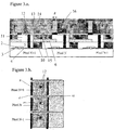
- Figure 1 shows an active matrix pixel where the display media is voltage controlled, such as liquid crystal or electronic paper.
- Figure 1.a is a side view of one transistor and one pixel. It consists of a substrate 1, a semiconductor 2, which may be a continuous layer or may be patterned, (in Figure 1 , the semiconductor is patterned in order to cover the transistor channel), a data line 3, a pixel electrode 4, a transistor dielectric 5, a gate electrode/gate interconnect 6 and a display media 7 (for example liquid crystal or electronic paper) and a counter electrode 8 of the display media.
- the state of the display media is determined by the electric field across the media, which is a function of the voltage difference between the pixel electrode 4 and the counter electrode 8.
- a switchable area of the device 9 can be switched by a voltage difference between the pixel 4 and the top electrode 8. This area determines the aperture ratio of the device.
- Figure 1.b is a top view of the device and shows six transistors and six pixels arranged in three rows. (The display media is not shown in Figure 1.b ).
- the lines are written sequentially.
- the voltage written to one line should remain relatively constant during the addressing of the other lines.
- the pixel acts as a parallel plate capacitor providing a reservoir of charge.
- This capacitance can be augmented by the inclusion of a storage capacitor.
- a storage capacitor can be formed by overlapping the pixel with the gate line of the neighbouring transistor.
- Figure 2 explains the incorporation of a pixel capacitor into a transistor-controlled display device, for the case where the drain electrode is the pixel electrode, and is a schematic diagram of three adjacent pixels, N-1, N and N+1 of a top gate device.
- Figure 2.a shows the side view of the device.
- the gates/gate interconnects 6 are extended to overlap part of the adjacent pixel.
- a capacitor 10 is formed between pixel N and the gate of pixel N-1.
- the resultant storage capacitor helps the pixel to maintain a constant voltage throughout the cycle.
- this overlap of the adjacent gate interconnect over the lower, drain (pixel) electrode leads to a reduction of the switchable area 9 of the device and therefore, the aperture ratio.
- FIG. 2c shows the circuit diagram for this arrangement, where the storage capacitor, C storage , is formed between the pixel electrode 4 and the gate of a pixel of a neighbouring transistor. This capacitor acts as a reservoir for charge and therefore enhances the image holding ability of the pixel.
- Figure 3 incorporates a pixel capacitor that allows for a high aperture ratio.
- Figure 3.a shows the side view of three adjacent transistors and pixels.
- Figure 3.b illustrates a top view of six pixels. Three of these pixel electrodes are shown as being semitransparent, for clarity.
- Data addressing lines 20 running across the display, TFT source electrodes 3, and TFT drain electrodes 4 are formed on a first metal level of the device.
- a metal level is defined as a layer of the device that contains conductive interconnects and / or conductive electrodes.
- the patterned pixel electrode 13 forming one of the contacts to the display element 14 is formed on a separate, second metal level of the device.
- the TFT gate electrode 24, the gate addressing row interconnects 22 and the counter electrode of the pixel capacitor 6 are formed on a third metal level of the device.
- In between the first and third metal level and the second and third metal level is at least one dielectric layer 5, 11 which provides electrical insulation between the electrodes and interconnects at different levels.
- the dielectric between the first and third level is the gate dielectric 5 of the TFT.
- the pixel electrode 13 on the second level is electrically connected to the drain electrode 4 on the first level.
- the latter is achieved by the formation of a via-hole interconnection 12. This interconnection is formed both through the dielectric layer 11 between the second and third levels, and the dielectric layer 5 between the first and third levels.
- the source and drain electrodes 3, 4 may be formed as follows.
- a surface energy pattern is defined on a substrate that consists of an array of hydrophobic and hydrophilic regions. This surface energy pattern is formed as a result of a hydrophobic polymer, such as polyimide (PI), being deposited and patterned on top of a hydrophilic glass substrate.
- PI polyimide
- the source and drain electrodes are deposited through ink jet printing from a liquid material, such as PEDOT/PSS, within the hydrophilic wells.
- the hydrophobic ridges define the TFT channel.
- the pixel electrodes 13 of neighbouring pixels on the second metal level may be printed with a small distance of typically on the order of 15-20 ⁇ m between each other. This small gap between neighbouring pixel electrodes needs to be defined very reliably in order to avoid electrical shorting from one pixel to the next.
- a surface energy pattern 16 can be predefined on the second metal level prior to the deposition of the pixel electrodes 13 to repel the ink of the conducting pixel electrode material, and define accurately the dimensions of the pixel electrode.
- the surface energy pattern can be defined by techniques such as laser forward transfer printing, photolithographic patterning, laser direct write patterning, soft lithographic stamping, embossing, inkjet deposition, or other direct-write deposition and patterning techniques.
- FIG. 4 An embodiment of the present invention and its method of production is shown in Figure 4 .
- This configuration is a variation of the architecture shown in Figure 3 .
- either one or both of the dielectric layers 5, 11 are patterned and the pixel electrode 13 is formed partially on the first level and partially on the second level with a metallic interconnection formed across a side wall of the patterned dielectric(s).
- the dielectric layer(s) are patterned by direct-write deposition, such as, for example, inkjet printing or screen printing.
- the pixel electrode 13 is also deposited by direct-write printing, for example, by printing a conductive material over the sidewalls of the dielectric pattern to form the electrical connection between the pixel electrode 13 and the drain electrode 4.
- the pattern of the dielectric layers 5, 11 is defined in such a way that adequate isolation is achieved between the gate electrodes / interconnects 22, 24 on the third level, and the other electrodes 3, 4, 13 on the first and second levels.
- One advantage of the configuration illustrated in Figure 4 is that it does not require formation of a via-hole interconnection, although the area on the first and third level that is available for electrodes and interconnects is reduced compared to the configuration shown in Figure 3 .
- the pixel capacitor is formed between the pixel capacitor counter electrode 6 which is connected to the gate addressing lines of the (N-1) or (N+1)th row of pixels, and the pixel electrode 13 on the third level. It is also possible to form an additional capacitor 10 between the pixel capacitor counter electrode 6 on the third level, and an extension of the drain electrode 4 on the first level (see also Figure 3 ). This increases the total capacitance of the pixel capacitor for a given area of the pixel capacitor counter electrode 6.
- each pixel electrode covers the respective pixel area of the second level almost completely with only a small gap of dimension d left to the neighbouring pixels. This achieves aperture ratios close to 100 %.
- This configuration has the following additional advantages.
- the width of the data addressing lines 20 can be made relatively large in order to achieve better conductivity.
- the width of the channel of the TFT can be increased by, for example forming the source and drain electrodes 3, 4 in an interdigitated configuration or by forming the source electrode 3 on all four sides of the pixel.
- the source and drain electrodes 3, 4 can cover a significant fraction of the area of the first level.
- the width of the gate addressing interconnects can be increased in order to achieve a better conductivity.
- the size of the pixel capacitor counter electrode 6 and its lateral overlap with the pixel electrode 13 may be adjusted so that it occupies a significant fraction of the area of the third level.
- the device components (interconnects, electrodes, semiconductor and insulating elements) of each of the above mentioned embodiments are deposited by solution processing and / or direct printing. This may be done, for example, by inkjet printing, aerosol printing, offset printing, solution or blade coating.
- a surface energy pattern may be formed on the substrate prior to deposition of the electrodes and interconnects on each level. Surface energy patterning can be achieved by a range of techniques including, but not limited to photolithography, microcontact printing or exposure to focussed electromagnetic radiation (see WO02/095805 The surface energy pattern makes the surface regions that are to be kept free of conducting material repulsive for the ink of the conducting material. This allows printing of narrow interconnect lines and electrodes, and also allows to minimize the size of any gaps required between different electrodes on the same metal level, such as the distance d. Surface energy patterning can be performed on any of the metal levels prior to deposition of the conductive material.
- Via hole formation is preferably carried out by a direct-write based method such as laser ablation or ink jetting of solvent.
- via holes may also be made by other methods such as mechanical means or photolithography.
- the via-hole After the via-hole is formed it can be filled with conductive material, preferably using a print based method such as inkjet.
- the above three-metal level configuration allows to achieve high values of the capacitance of the pixel capacitor, while maintaining high aperture ratios, that can in principle be close to 100%. This is true whether the electrodes and interconnects are formed from optically transparent conductive material or not.
- high aperture ratios can be achieved by using transparent conductive materials, such as PEDOT/PSS or ITO for all electrodes that occupy a large area.
- transparent conductive materials such as PEDOT/PSS or ITO for all electrodes that occupy a large area.
- the use of non-transparent conductors may be restricted to ones such as inkjet printed or aerosol printed colloidal metal in the case of interconnects that require a high conductivity close to that of bulk copper or silver, such as the long gate addressing interconnects and the data addressing interconnects running across the display.
- the pixel electrode, the pixel capacitor counter electrode, the via-hole interconnection and the source/drain/gate electrodes may all be formed from a transparent conductor such as printable transparent tin oxides or PEDOT/PSS.
- a conducting via-hole interconnection 12 runs from the drain electrode 4 of the transistor through the dielectric and insulating layers to an enlarged pixel electrode 13.
- the switchable area of the display medium 14 and therefore the aperture ratio is enlarged and can be close to 100%.
- the storage capacitor 10 can be increased.
- This device structure also allows the pixel capacitor to be double sided. For example, a capacitor is formed between a) the middle and the lower level and b) the middle and upper level. This provides the capability to produce a very large pixel capacitor whilst maintaining an aperture ratio of near 100%.
- FIG. 4a shows a display structure built up to the gate level, with extended gates as described previously.
- the insulating layers, 5 and 11 are patterned so as only to isolate the necessary components of the metal layers.
- Figure 4.b a conducting interconnect 12 is formed between the drain electrode 4 and the upper, pixel electrode 13.
- the connecting interconnect need only be deposited by solvent or mechanical methods, since there is no requirement to form a via-hole.
- the upper insulating layer could be patterned requiring a via-hole to be formed only through the lower dielectric layer.
- one possibility for patterning the pixel electrodes such that they make contact with the electrodes without shorting is to choose the lower dielectric 5 and the pixel electrode material 13 such that the lower dielectric material will repel the pixel electrode material as it is printed.
- the upper dielectric material 11 is chosen such that the pixel electrode material adheres well. On the area of the pixel where contact to the lower electrode is required, the upper dielectric material covers the lower dielectric material. On other areas of the pixel, the upper dielectric material does not overlap the lower dielectric material. This creates a channel that is repulsive to the pixel electrode material as it is being printed and can reduce the need for high print accuracy.
- the device of the present invention may be used with voltage controlled display media such as liquid crystal or electronic paper, but also with current-driven displays, such as organic light-emitting diode displays. It may be used in both reflective and transmissive displays. The display effect and the nature of the display influence the design of the active matrix.
- all layers of the active matrix TFT array are deposited from solution, and patterned by direct printing techniques.
- Some of the layers such as the interconnect lines requiring a high conductivity might be deposited by vacuum deposition techniques and patterned by photolithography.
- the conductivity of the gate lines and data lines has to be high for the display to fully operate. If these lines are accurately printed and/or confined by surface energy patterning they can be made from very high conductivity, low transparency materials such as colloidal metals that can be used without overly diminishing the overall transparency of the display. Alternately transparent conductors may be used if the conductivity is sufficiently high.
- the conductivity of the material of any of the pixel electrodes does not have to be as high as the gate lines and data lines.
- PEDOT, ITO or other transparent conductors may be used.
- metals can be used for the upper, pixel electrode, providing the necessary reflectivity.
- the display structure is formed on a substrate, which could be produced of glass, plastic, stainless steel or other materials.
- the data lines are formed from conducting material. They are preferentially formed by printing, although evaporation and photolithography may also be used. In the case where the data lines are printed they can either be printed using accurate printing alone or surface energy assisted patterning. Examples for print methods are ink jet printing, aerosol printing, offset printing, screen printing, lithography and gravure printing.
- the printed material could be colloidal metal or a conducting polymer such as PEDOT. Where the display effect is transmissive, very fine lines can be formed by accurate printing or other deposition methods, or, a transparent conductor may be deposited, such as PEDOT or ITO. These lines should be sufficiently conducting for display operation.
- the semiconductor layer is preferentially deposited from solution although it may also be deposited by evaporation.
- the semiconducting material might be a small organic molecule or a conjugated polymer, or a solution-processible inorganic semiconductor, such as a dispersion of inorganic nanoparticles.
- the semiconducting layer is patterned into active layer islands in order to reduce parasitic leakage currents between neighbouring pixels and devices.
- the semiconducting material may be deposited by inkjet printing. In addition, surface energy patterning may be used to enhance the printing resolution.
- the gates and interconnects are formed from conducting material. They are preferentially formed by printing, although evaporation and the techniques of photolithography may also be used.
- the gates and interconnects may either be printed using accurate printing alone or surface energy patterning. Examples of print methods that may be used include inkjet printing, aerosol printing, offset printing screen printing, and gravure printing.
- the material printed could be colloidal metal or a conducting polymer such as PEDOT. Where the display effect is transmisive very fine lines can be formed by accurate printing or other deposition methods, or, a transparent conductor such as PEDOT or ITO can be used.
- the lines should also be sufficiently conducting in order to minimize RC delays along the gate lines.
- the deposition process used should be compatible with the layers that have been previously deposited.
- the pixel electrode is formed preferably by printing but may also be formed by other methods such as evaporation and photolithography. Examples of print methods that can be used include inkjet printing, aerosol printing, offset printing screen printing, and gravure printing.
- the material printed could be colloidal metal or a conducting polymer such as PEDOT. Where the display effect is transmissive a transparent conductor such as PEDOT can be used.
- the deposition process used for both layers should be compatible with previously deposited layers, the via-hole and double dielectric layer formation.
- the upper, pixel electrode 13 determines the aperture ratio. Minimising the dimension d (see Figure 3 ) increases the aperture ratio. This can be done through any of the patterning methods such as photolithography but is preferentially achieved by printing techniques, either by accurate printing alone or printing combined with surface energy patterning. Preferably, surface energy assisted printing is used in order to minimize the distance d, and to reduce the risk of defects and shorts between adjacent pixels.
- Surface energy patterning on the surface of the dielectric layer 11 can be achieved by a range of techniques including, but not limited to photolithography, microcontact printing or exposure to focussed electromagnetic radiation ( WO02/095805 ). The surface energy pattern enables the surface regions with width d to repulse the ink of the conducting pixel electrode and allows accurate printing with minimum d.
- the dielectric layers are preferentially deposited from solution although other methods such as evaporation may be used. Where deposited from solvents care should be taken that the bottom layer is insoluble in the solvent of the top dielectric layer.
- the upper dielectric layer may be deposited in a patterned fashion by inkjet printing, aerosol printing or other methods, so as to cover the gates and gate lines and such as to define the pixel capacitor area. Where the dielectrics layer are patterned, the upper, pixel electrode can be deposited by any of the methods as described above, in direct contact with the lower pixel electrode, thus removing the need for via-hole formation as described below
- unwanted scattering of light can be avoided by either patterning the dielectric layers so as to cover a minimal area of the display and/or well matching their refractive index to those of the surrounding.
- the via-hole can be formed by a broad range of techniques, such as, but not limited to, laser ablation, photolithography or mechanical methods.
- a preferred method is the printing of solvents and subsequent filling with conductive material as described in WO01/47045 .
- the via-hole is formed by the printing of solvents and it has to penetrate two dielectric layers and in some cases a semiconducting layer. For this a sequence of different solvents or a blend of two or more solvents can be used.
- the via-hole should be sufficiently small to fit within the pixel area without interfering with the transistor.
- the via-hole should be ⁇ 100 microns in diameter and most preferably ⁇ 50 microns in diameter.
- the surface of the pixel electrode in the vicinity of the via-hole and above the via-hole should be smooth.
- the via-hole can be formed from transparent material such as PEDOT.
- the via-hole is filled with a conducting material that has a similar refractive index to that of the dielectric layer in order to reduce any light scattering.
- the optical inhomogeneity around the via-hole is too high, the area of the via-hole can be shielded from the viewer by a black matrix.
- Another preferred method for the forming of via holes is laser ablation.
- the dielectric materials are removed in a selective fashion by the rapid absorption of energy from a scanning laser beam to form via holes.
- the dielectric layers used can either be intrinsically absorbing or are mixed with a dye to increase the absorption at the wavelength of the laser beam.
- Another method incorporating laser ablation is to deposit a release layer before the dielectric layers are deposited. This release layer is highly absorbing to the wavelength of the laser beam and on absorption removes the dielectric layers deposited on top.
- via holes are then filled with a conducting material, preferably using a print based method such as ink jet.
- the architecture shown in Figure 3 is a three level device architecture incorporating a double-sided capacitor and large aperture ratio.
- a via hole is formed between the first and third level and the third and second level to ensure electrical conduction between the levels.
- the source and drain electrodes 3, 4, which consist of a conductive material such as PEDOT/PSS, may be deposited on the first metal level by a technique such as inkjet printing. Inkjet printed colloidal silver may be confined by surface energy patterning to form data lines 20.
- the semiconductor 2 which may consist of a material such as poly(dioctylfluorene-co-bithiophene) (F8T2) in a solution of xylene may be deposited by a technique such as inkjet printing into an active layer island, in order to reduce parasitic leakage currents between neighbouring pixels and devices.
- a continuous dielectric layer 5 may be deposited by techniques such as spin-coating to provide electrical insulation between the electrodes and connections at different levels.
- a suitable material for such an insulating layer may be polymethylmethacrylate (PMMA).
- PMMA polymethylmethacrylate
- the gate electrode 24, and gate addressing lines 22 are formed by the deposition of a conductive material such as colloidal silver or PEDOT/PSS.
- the pixel capacitor counter electrode 6 is also on the third metal level. This is followed by a second continuous dielectric layer of polystyrene deposited in between the third and second metal layer of the device by spin-coating, blade coating or other solution processing techniques.
- a patterned pixel electrode forming one of the contacts to the display element 13 is formed on a separate, second metal level of the device.
- the pixel electrodes on metal levels 6, 13 may be formed by inkjet printed PEDOT or ITO or other transparent conductors (transmissive display) or colloidal silver (reflective display).
- the pixel capacitor is formed between the pixel capacitor counter electrode 6 which is connected to the gate addressing lines 22 and the pixel electrode 13 on the third level. It is also possible to form an additional capacitor between the pixel capacitor counter electrode 13 on the third level, and an extension of the drain electrode 4 on the first level. The formation of this double-sided capacitor has been seen to increase the total capacitance of the pixel capacitor for a given area of the counter electrode.
- a via-hole is formed.
- the via-hole is formed between the pixels on each metal level of the device.
- a via-hole may be formed either by printing techniques or by methods of laser ablation.
- Printing techniques such as, but not limited to inkjet printing may be used to produce a via-hole in the above described device.
- a solvent or mixture of solvents is deposited that are able to dissolve both the first and second dielectric material, but differentiates between lower pixels.
- ethyl acetate may be used as a suitable solvent.
- the resultant via-hole may then be filled with a conductive material, forming a connection between the two pixels, such as PEDOT.
- the via channels may be formed either by using a rastering laser where the wavelength of the laser is absorbed by the dielectric materials or where an absorbing dye is added to the dielectric layers.
- Such a system would allow successful via-hole formation by virtue of the non-solubility of the dielectric layers in the via-hole solvent.
- a three level device architecture incorporates polyvinylphenol (PVP) as the gate dielectric 5, followed by polystyrene for the second dielectric layer 11.
- PVP polyvinylphenol
- Isopropanol and xylene or xexane are possible solvents for the formation of the via-holes in these layers, although as mentioned above, this embodiment can be produced without forming via-holes.
- the semiconductor 2 which may consist of a material such as poly(dioctylfluorene-co-bithiophene) (F8T2) in a solution such as xylene may be deposited by a technique such as inkjet printing into an active layer island, in order to reduce parasitic leakage currents between neighbouring pixels and devices.
- a patterned dielectric layer 5 of polyvinylphenol (PVP) may be deposited by a technique such as inkjet printing on a surface energy pattern, as previously described or other patterning techniques in order to provide adequate isolation between the gate electrodes and the interconnects on the third level and electrodes on the first and second level.
- PVP polyvinylphenol
- the gate electrode 24 and gate addressing lines 22 are formed by the deposition of a conductive material such as colloidal silver or PEDOT/PSS.
- a pixel capacitor counter electrode 6 is also on the third metal level.
- a patterned pixel electrode forming one of the contacts to the display element 13 is formed partially on the first level and partially on the second level of the device with a metallic connection formed across a side wall of the patterned dielectric(s).
- the pixel electrode 13 may be formed by inkjet printed PEDOT or ITO or other transparent conductors (transmissive display) or colloidal silver (reflective display).
- the combination of materials and processes used to fabricate this invention are ideally tailored to the end use of the device.
- a reflective display there is no need for the active matrix backplane components to be transparent.
- a transmissive display one arrangement would incorporate a combination of high conductivity, highly confined opaque conducting materials with lower conductivity transparent conductors.
- the highly conducting, well confined materials for example colloidal silver, which can be deposited in many ways including surface energy assisted printing or aerosol, would be used as the data lines and interconnect lines.
- the confined nature of these features means that the transmission of the display is not seriously affected.
- the transparent, lower conductivity elements for example ITO or PEDOT, which can also be deposited using printing or other methods, are used for the pixel and storage capacitance electrodes. This combination of high conductivity and high resolution patterned layers combined with low conductivity transparent layers enables the fabrication of a print based transparent display with high aperture ratio and high pixel capacitance.
- the conducting electrodes of the TFT and/or the connections in the display device may be formed from inorganic conductors that may, for example, be deposited by the printing of a colloidal suspension or by electroplating onto a pre-patterned substrate.
- inorganic conductors may, for example, be deposited by the printing of a colloidal suspension or by electroplating onto a pre-patterned substrate.
- one or more of the conductive components of the device may be formed from an insoluble conductive material such as a vacuum-deposited conductor.
- Any solution processible conjugated polymeric or oligomeric material that exhibits adequate field-effect mobilities exceeding 10 -3 cm 2 /Vs, preferably exceeding 10 -2 cm 2 /Vs , may be used for the formation of the semiconducting layer.
- Suitable materials are reviewed in H.E. Katz, J. Mater. Chem. 7, 369 (1997 ), or Z. Bao, Advanced Materials 12, 227 (2000).
- Other possibilities include small conjugated molecules with solubilising side chains ( J.G. Laquindanum, et al., J. Am. Chem. Soc. 120, 664 (1998 )), semiconducting organic-inorganic hybrid materials self-assembled from solution ( C.R.
- the electrodes may be coarse-patterned by techniques other than inkjet printing. Suitable techniques include soft lithographic printing ( J.A. Rogers et al., Appl. Phys. Lett. 75, 1010 (1999 ); S. Brittain et al., Physics World May 1998, p. 31 ), screen printing ( Z. Bao, et al., Chem. Mat.
- Ink-jet printing is considered to be particularly suitable for large area patterning with good registration, in particular for flexible plastic substrates.
- all layers and components of the device and circuit are deposited and patterned by solution processing and printing techniques, one or more components may also be deposited by vacuum deposition techniques and/or patterned by a photolithographic process.
Landscapes
- Physics & Mathematics (AREA)
- Nonlinear Science (AREA)
- Optics & Photonics (AREA)
- General Physics & Mathematics (AREA)
- Microelectronics & Electronic Packaging (AREA)
- Engineering & Computer Science (AREA)
- Mathematical Physics (AREA)
- Crystallography & Structural Chemistry (AREA)
- Chemical & Material Sciences (AREA)
- Geometry (AREA)
- Devices For Indicating Variable Information By Combining Individual Elements (AREA)
- Thin Film Transistor (AREA)
- Liquid Crystal (AREA)
Description
- This invention relates, in one aspect, to transistor-controlled display devices and techniques of use in their production, and in one embodiment to active matrix polymer TFT displays, having enhanced aperture ratios and pixel storage capacitors, more specifically the formation of high-resolution active matrix displays using techniques based on solution processing and direct printing.
The most common active matrix display technology is the thin film transistor liquid crystal display (LCD), where applications range from PDA and notebook devices to flat screen televisions. Active matrix displays are also used in combination with emerging display effects such as organic light emitting diodes (OLED) and electronic paper.
A TFT device configuration is described inWO01/47045
Semiconducting conjugated polymer thin-film transistors (TFTs) have recently become of interest for applications in active-matrix displays, primarily due to their solution processibility and consequential printability. Such polymers were used as the active material to create a 4096 active matrix pixel display with 256 grey levels (E.A. Huitema et al., Nature 414, 599 (2001)). Semiconducting polymers in solution based print processes have more recently been used to create active matrix displays with printed polymer thin film transistors (S. Burns, et al. SID 2002 symposium, Digest of Technical Papers 33, 1193 (2002)).
One problem can be the limited display area, in particular for high-resolution displays, in which the thin film transistor, particularly the drain (pixel) electrode, and other components, such as the data and addressing lines, and the pixel capacitor compete with each other for space. This can lead to a reduction in the aperture ratio and therefore the quality of the display. In order to achieve a high aperture ratio, the area of the pixel electrode should be as large as possible. This is particularly difficult to achieve in conventional architectures, if the pixel electrode is defined on the same level as any of the gate or addressing lines, or any of the electrodes of the TFT. - The manufacture of active matrix displays by solution based print processes offers many potential advantages over conventional manufacturing methods. In principle, solution based print processes are environmentally friendly, low temperature, compatible with flexible substrates, cost effective and advantageous for short run length and large display sizes. However, fabrication of high-resolution displays by printing processes is challenging. When using printing processes such as inkjet printing, screen printing and offset printing, it is difficult to fabricate metallic interconnect lines with a width of less than 50 -100 µm because of the difficulties associated with delivering small volumes of liquid. This problem can be alleviated somewhat by printing onto a substrate with a predefined surface energy pattern as disclosed in
PCT/GB00/04934 -
- Accordingly, it is one aim of the present invention to provide a thin film transistor device incorporating an architecture resulting in a high aperture ratio and, preferably, allowing for good pixel capacitance.
- According to the present invention, there is provided an electronic device according to
claim 1. - To help understanding of the invention, a specific embodiment thereof will now be described by way of example and with reference to the accompanying drawings, in which:
-
Figure 1 shows the general structure of an active matrix display pixel. -
Figure 2 explains the incorporation of a pixel capacitor into a transistor-controlled display device, for the case where the drain electrode is the pixel electrode. -
Figure 3 shows a device not in accordance with the claimed invention. -
Figure 4 shows a device according to an embodiment of the present invention. -
Figure 5 shows a bottom gate device not in accordance with the claimed invention. -
Figure 1 shows an active matrix pixel where the display media is voltage controlled, such as liquid crystal or electronic paper.Figure 1.a . is a side view of one transistor and one pixel. It consists of asubstrate 1, asemiconductor 2, which may be a continuous layer or may be patterned, (inFigure 1 , the semiconductor is patterned in order to cover the transistor channel), adata line 3, apixel electrode 4, a transistor dielectric 5, a gate electrode/gate interconnect 6 and a display media 7 (for example liquid crystal or electronic paper) and acounter electrode 8 of the display media. In such a system the state of the display media is determined by the electric field across the media, which is a function of the voltage difference between thepixel electrode 4 and thecounter electrode 8. A switchable area of thedevice 9 can be switched by a voltage difference between thepixel 4 and thetop electrode 8. This area determines the aperture ratio of the device. -
Figure 1.b . is a top view of the device and shows six transistors and six pixels arranged in three rows. (The display media is not shown inFigure 1.b ). - In an active matrix array, the lines are written sequentially. In order to maintain an image, the voltage written to one line should remain relatively constant during the addressing of the other lines. This is particularly true of greyscale devices. In voltage controlled devices, the pixel acts as a parallel plate capacitor providing a reservoir of charge. This capacitance can be augmented by the inclusion of a storage capacitor. A storage capacitor can be formed by overlapping the pixel with the gate line of the neighbouring transistor.
Figure 2 explains the incorporation of a pixel capacitor into a transistor-controlled display device, for the case where the drain electrode is the pixel electrode, and is a schematic diagram of three adjacent pixels, N-1, N and N+1 of a top gate device.Figure 2.a . shows the side view of the device. The gates/gate interconnects 6 are extended to overlap part of the adjacent pixel. Acapacitor 10 is formed between pixel N and the gate of pixel N-1. The resultant storage capacitor helps the pixel to maintain a constant voltage throughout the cycle. However, in this case, this overlap of the adjacent gate interconnect over the lower, drain (pixel) electrode leads to a reduction of theswitchable area 9 of the device and therefore, the aperture ratio. -
Figure 2.c . shows the circuit diagram for this arrangement, where the storage capacitor, Cstorage, is formed between thepixel electrode 4 and the gate of a pixel of a neighbouring transistor. This capacitor acts as a reservoir for charge and therefore enhances the image holding ability of the pixel. - The architecture of
Figure 3 incorporates a pixel capacitor that allows for a high aperture ratio.Figure 3.a . shows the side view of three adjacent transistors and pixels.Figure 3.b illustrates a top view of six pixels. Three of these pixel electrodes are shown as being semitransparent, for clarity. -
Data addressing lines 20 running across the display,TFT source electrodes 3, andTFT drain electrodes 4 are formed on a first metal level of the device. A metal level is defined as a layer of the device that contains conductive interconnects and / or conductive electrodes. The patternedpixel electrode 13 forming one of the contacts to thedisplay element 14 is formed on a separate, second metal level of the device. TheTFT gate electrode 24, the gate addressingrow interconnects 22 and the counter electrode of thepixel capacitor 6 are formed on a third metal level of the device. In between the first and third metal level and the second and third metal level is at least onedielectric layer Figure 3 the dielectric between the first and third level is the gate dielectric 5 of the TFT. - The
pixel electrode 13 on the second level is electrically connected to thedrain electrode 4 on the first level. In the configuration shown inFigure 3 , the latter is achieved by the formation of a via-hole interconnection 12. This interconnection is formed both through thedielectric layer 11 between the second and third levels, and thedielectric layer 5 between the first and third levels. - The source and
drain electrodes - In order to achieve a particularly high aperture ratio the
pixel electrodes 13 of neighbouring pixels on the second metal level may be printed with a small distance of typically on the order of 15-20 µm between each other. This small gap between neighbouring pixel electrodes needs to be defined very reliably in order to avoid electrical shorting from one pixel to the next. Asurface energy pattern 16 can be predefined on the second metal level prior to the deposition of thepixel electrodes 13 to repel the ink of the conducting pixel electrode material, and define accurately the dimensions of the pixel electrode. The surface energy pattern can be defined by techniques such as laser forward transfer printing, photolithographic patterning, laser direct write patterning, soft lithographic stamping, embossing, inkjet deposition, or other direct-write deposition and patterning techniques. - An embodiment of the present invention and its method of production is shown in
Figure 4 . This configuration is a variation of the architecture shown inFigure 3 . In the present embodiment either one or both of thedielectric layers pixel electrode 13 is formed partially on the first level and partially on the second level with a metallic interconnection formed across a side wall of the patterned dielectric(s). According to one preferred aspect of this embodiment, the dielectric layer(s) are patterned by direct-write deposition, such as, for example, inkjet printing or screen printing. Preferably thepixel electrode 13 is also deposited by direct-write printing, for example, by printing a conductive material over the sidewalls of the dielectric pattern to form the electrical connection between thepixel electrode 13 and thedrain electrode 4. The pattern of thedielectric layers other electrodes Figure 4 is that it does not require formation of a via-hole interconnection, although the area on the first and third level that is available for electrodes and interconnects is reduced compared to the configuration shown inFigure 3 . - The pixel capacitor is formed between the pixel
capacitor counter electrode 6 which is connected to the gate addressing lines of the (N-1) or (N+1)th row of pixels, and thepixel electrode 13 on the third level. It is also possible to form anadditional capacitor 10 between the pixelcapacitor counter electrode 6 on the third level, and an extension of thedrain electrode 4 on the first level (see alsoFigure 3 ). This increases the total capacitance of the pixel capacitor for a given area of the pixelcapacitor counter electrode 6. - On each level, the electrodes and interconnects can occupy a significant fraction of the pixel area. In the present embodiment, each pixel electrode covers the respective pixel area of the second level almost completely with only a small gap of dimension d left to the neighbouring pixels. This achieves aperture ratios close to 100 %. This configuration has the following additional advantages. On the first level the width of the
data addressing lines 20 can be made relatively large in order to achieve better conductivity. The width of the channel of the TFT can be increased by, for example forming the source anddrain electrodes source electrode 3 on all four sides of the pixel. The source anddrain electrodes capacitor counter electrode 6 and its lateral overlap with thepixel electrode 13 may be adjusted so that it occupies a significant fraction of the area of the third level. - Preferably all of the device components (interconnects, electrodes, semiconductor and insulating elements) of each of the above mentioned embodiments are deposited by solution processing and / or direct printing. This may be done, for example, by inkjet printing, aerosol printing, offset printing, solution or blade coating. To achieve a high resolution of such solution deposition steps, a surface energy pattern may be formed on the substrate prior to deposition of the electrodes and interconnects on each level. Surface energy patterning can be achieved by a range of techniques including, but not limited to photolithography, microcontact printing or exposure to focussed electromagnetic radiation (see
WO02/095805 - Via hole formation is preferably carried out by a direct-write based method such as laser ablation or ink jetting of solvent. However, via holes may also be made by other methods such as mechanical means or photolithography. After the via-hole is formed it can be filled with conductive material, preferably using a print based method such as inkjet.
- In a reflective display where the pixel electrode itself is formed from a highly reflective metal such as silver or gold, such that the light does not pass through the first and third metal level, the above three-metal level configuration allows to achieve high values of the capacitance of the pixel capacitor, while maintaining high aperture ratios, that can in principle be close to 100%. This is true whether the electrodes and interconnects are formed from optically transparent conductive material or not.
- In a transmissive display, or in a reflective display where the reflective mirror is formed behind the active matrix such that the light passes through the layers of the active matrix array, high aperture ratios can be achieved by using transparent conductive materials, such as PEDOT/PSS or ITO for all electrodes that occupy a large area. The use of non-transparent conductors may be restricted to ones such as inkjet printed or aerosol printed colloidal metal in the case of interconnects that require a high conductivity close to that of bulk copper or silver, such as the long gate addressing interconnects and the data addressing interconnects running across the display. The pixel electrode, the pixel capacitor counter electrode, the via-hole interconnection and the source/drain/gate electrodes may all be formed from a transparent conductor such as printable transparent tin oxides or PEDOT/PSS.
- In the configuration illustrated in
Figure 3 , above the gate level, there is a further insulatinglayer 11. A conducting via-hole interconnection 12 runs from thedrain electrode 4 of the transistor through the dielectric and insulating layers to anenlarged pixel electrode 13. The switchable area of thedisplay medium 14 and therefore the aperture ratio is enlarged and can be close to 100%. Similarly, thestorage capacitor 10 can be increased.
This device structure also allows the pixel capacitor to be double sided. For example, a capacitor is formed between a) the middle and the lower level and b) the middle and upper level. This provides the capability to produce a very large pixel capacitor whilst maintaining an aperture ratio of near 100%.
Another method of achieving the same effect as the structure inFigure 3 is to pattern the dielectric layers such as to cover only the parts of the metal layers that we need to isolate.
Figure 4.a . shows a display structure built up to the gate level, with extended gates as described previously. The insulating layers, 5 and 11 are patterned so as only to isolate the necessary components of the metal layers. InFigure 4.b . a conductinginterconnect 12 is formed between thedrain electrode 4 and the upper,pixel electrode 13. The advantage of this structure is that the connecting interconnect need only be deposited by solvent or mechanical methods, since there is no requirement to form a via-hole. Similarly, the upper insulating layer could be patterned requiring a via-hole to be formed only through the lower dielectric layer.
For the method described above, one possibility for patterning the pixel electrodes such that they make contact with the electrodes without shorting is to choose thelower dielectric 5 and thepixel electrode material 13 such that the lower dielectric material will repel the pixel electrode material as it is printed. The upperdielectric material 11 is chosen such that the pixel electrode material adheres well. On the area of the pixel where contact to the lower electrode is required, the upper dielectric material covers the lower dielectric material. On other areas of the pixel, the upper dielectric material does not overlap the lower dielectric material. This creates a channel that is repulsive to the pixel electrode material as it is being printed and can reduce the need for high print accuracy. - The device of the present invention may be used with voltage controlled display media such as liquid crystal or electronic paper, but also with current-driven displays, such as organic light-emitting diode displays. It may be used in both reflective and transmissive displays. The display effect and the nature of the display influence the design of the active matrix.
- Preferably, all layers of the active matrix TFT array are deposited from solution, and patterned by direct printing techniques. Some of the layers such as the interconnect lines requiring a high conductivity might be deposited by vacuum deposition techniques and patterned by photolithography.
- The conductivity of the gate lines and data lines has to be high for the display to fully operate. If these lines are accurately printed and/or confined by surface energy patterning they can be made from very high conductivity, low transparency materials such as colloidal metals that can be used without overly diminishing the overall transparency of the display. Alternately transparent conductors may be used if the conductivity is sufficiently high.
- The conductivity of the material of any of the pixel electrodes does not have to be as high as the gate lines and data lines. In the case of transmissive displays, PEDOT, ITO or other transparent conductors may be used. For a reflective display, metals can be used for the upper, pixel electrode, providing the necessary reflectivity.
- The display structure is formed on a substrate, which could be produced of glass, plastic, stainless steel or other materials. The data lines are formed from conducting material. They are preferentially formed by printing, although evaporation and photolithography may also be used. In the case where the data lines are printed they can either be printed using accurate printing alone or surface energy assisted patterning. Examples for print methods are ink jet printing, aerosol printing, offset printing, screen printing, lithography and gravure printing. The printed material could be colloidal metal or a conducting polymer such as PEDOT. Where the display effect is transmissive, very fine lines can be formed by accurate printing or other deposition methods, or, a transparent conductor may be deposited, such as PEDOT or ITO. These lines should be sufficiently conducting for display operation.
- The semiconductor layer is preferentially deposited from solution although it may also be deposited by evaporation. The semiconducting material might be a small organic molecule or a conjugated polymer, or a solution-processible inorganic semiconductor, such as a dispersion of inorganic nanoparticles. Preferably, the semiconducting layer is patterned into active layer islands in order to reduce parasitic leakage currents between neighbouring pixels and devices. The semiconducting material may be deposited by inkjet printing. In addition, surface energy patterning may be used to enhance the printing resolution.
- The gates and interconnects are formed from conducting material. They are preferentially formed by printing, although evaporation and the techniques of photolithography may also be used. The gates and interconnects may either be printed using accurate printing alone or surface energy patterning. Examples of print methods that may be used include inkjet printing, aerosol printing, offset printing screen printing, and gravure printing. The material printed could be colloidal metal or a conducting polymer such as PEDOT. Where the display effect is transmisive very fine lines can be formed by accurate printing or other deposition methods, or, a transparent conductor such as PEDOT or ITO can be used. The lines should also be sufficiently conducting in order to minimize RC delays along the gate lines. The deposition process used should be compatible with the layers that have been previously deposited.
- The pixel electrode is formed preferably by printing but may also be formed by other methods such as evaporation and photolithography. Examples of print methods that can be used include inkjet printing, aerosol printing, offset printing screen printing, and gravure printing. The material printed could be colloidal metal or a conducting polymer such as PEDOT. Where the display effect is transmissive a transparent conductor such as PEDOT can be used. The deposition process used for both layers should be compatible with previously deposited layers, the via-hole and double dielectric layer formation.
- The upper,
pixel electrode 13 determines the aperture ratio. Minimising the dimension d (seeFigure 3 ) increases the aperture ratio. This can be done through any of the patterning methods such as photolithography but is preferentially achieved by printing techniques, either by accurate printing alone or printing combined with surface energy patterning. Preferably, surface energy assisted printing is used in order to minimize the distance d, and to reduce the risk of defects and shorts between adjacent pixels. Surface energy patterning on the surface of thedielectric layer 11 can be achieved by a range of techniques including, but not limited to photolithography, microcontact printing or exposure to focussed electromagnetic radiation (WO02/095805 - The dielectric layers are preferentially deposited from solution although other methods such as evaporation may be used. Where deposited from solvents care should be taken that the bottom layer is insoluble in the solvent of the top dielectric layer. The upper dielectric layer may be deposited in a patterned fashion by inkjet printing, aerosol printing or other methods, so as to cover the gates and gate lines and such as to define the pixel capacitor area. Where the dielectrics layer are patterned, the upper, pixel electrode can be deposited by any of the methods as described above, in direct contact with the lower pixel electrode, thus removing the need for via-hole formation as described below
- For a transmissive effect display, unwanted scattering of light can be avoided by either patterning the dielectric layers so as to cover a minimal area of the display and/or well matching their refractive index to those of the surrounding.
- In the case of the via-hole connection configuration, the via-hole can be formed by a broad range of techniques, such as, but not limited to, laser ablation, photolithography or mechanical methods. A preferred method is the printing of solvents and subsequent filling with conductive material as described in
WO01/47045 - The architecture shown in
Figure 3 is a three level device architecture incorporating a double-sided capacitor and large aperture ratio. A via hole is formed between the first and third level and the third and second level to ensure electrical conduction between the levels. - The source and
drain electrodes semiconductor 2 which may consist of a material such as poly(dioctylfluorene-co-bithiophene) (F8T2) in a solution of xylene may be deposited by a technique such as inkjet printing into an active layer island, in order to reduce parasitic leakage currents between neighbouring pixels and devices. Acontinuous dielectric layer 5 may be deposited by techniques such as spin-coating to provide electrical insulation between the electrodes and connections at different levels. A suitable material for such an insulating layer may be polymethylmethacrylate (PMMA). On a third level of the device thegate electrode 24, andgate addressing lines 22 are formed by the deposition of a conductive material such as colloidal silver or PEDOT/PSS. Also on the third metal level is the pixelcapacitor counter electrode 6. This is followed by a second continuous dielectric layer of polystyrene deposited in between the third and second metal layer of the device by spin-coating, blade coating or other solution processing techniques. A patterned pixel electrode forming one of the contacts to thedisplay element 13 is formed on a separate, second metal level of the device. The pixel electrodes onmetal levels - As previously described, the pixel capacitor is formed between the pixel
capacitor counter electrode 6 which is connected to thegate addressing lines 22 and thepixel electrode 13 on the third level. It is also possible to form an additional capacitor between the pixelcapacitor counter electrode 13 on the third level, and an extension of thedrain electrode 4 on the first level. The formation of this double-sided capacitor has been seen to increase the total capacitance of the pixel capacitor for a given area of the counter electrode. - In order to ensure electrical conduction between the three levels of the device, a via-hole is formed. The via-hole is formed between the pixels on each metal level of the device. A via-hole may be formed either by printing techniques or by methods of laser ablation.
- Printing techniques such as, but not limited to inkjet printing may be used to produce a via-hole in the above described device. A solvent or mixture of solvents is deposited that are able to dissolve both the first and second dielectric material, but differentiates between lower pixels. In the case of the above mentioned PMMA dielectric layer, ethyl acetate may be used as a suitable solvent. The resultant via-hole may then be filled with a conductive material, forming a connection between the two pixels, such as PEDOT.
- Alternatively, a technique of laser ablation may be used. The via channels may be formed either by using a rastering laser where the wavelength of the laser is absorbed by the dielectric materials or where an absorbing dye is added to the dielectric layers. After the via channels are formed, they may be filled with a conductive material using techniques such as inkjet printing. Such a system would allow successful via-hole formation by virtue of the non-solubility of the dielectric layers in the via-hole solvent.
- In the embodiment shown in
Figure 4 a three level device architecture incorporates polyvinylphenol (PVP) as thegate dielectric 5, followed by polystyrene for thesecond dielectric layer 11. Isopropanol and xylene or xexane are possible solvents for the formation of the via-holes in these layers, although as mentioned above, this embodiment can be produced without forming via-holes. - The source and
drain electrodes semiconductor 2 which may consist of a material such as poly(dioctylfluorene-co-bithiophene) (F8T2) in a solution such as xylene may be deposited by a technique such as inkjet printing into an active layer island, in order to reduce parasitic leakage currents between neighbouring pixels and devices. A patterneddielectric layer 5 of polyvinylphenol (PVP) may be deposited by a technique such as inkjet printing on a surface energy pattern, as previously described or other patterning techniques in order to provide adequate isolation between the gate electrodes and the interconnects on the third level and electrodes on the first and second level. On a third level of the device thegate electrode 24 andgate addressing lines 22 are formed by the deposition of a conductive material such as colloidal silver or PEDOT/PSS. Also on the third metal level is a pixelcapacitor counter electrode 6. This is followed by a second patterned dielectric layer of polyvinylalcohol (PVA) deposited in between the third and second metal layer of the device by techniques such as inkjet printing or in a continuous film by techniques such as spin coating, blade coating or spray coating, followed by patterning techniques such as laser ablation. A patterned pixel electrode forming one of the contacts to thedisplay element 13 is formed partially on the first level and partially on the second level of the device with a metallic connection formed across a side wall of the patterned dielectric(s). Thepixel electrode 13 may be formed by inkjet printed PEDOT or ITO or other transparent conductors (transmissive display) or colloidal silver (reflective display). - As previously described a double-sided capacitor has again been formed, thereby increasing the total capacitance of the pixel capacitor for a given area of the counter electrode.
- There is no requirement for the formation of a via-hole interconnect to be incorporated within this device architecture.
- The combination of materials and processes used to fabricate this invention are ideally tailored to the end use of the device. For a reflective display, there is no need for the active matrix backplane components to be transparent. However, for a transmissive display, one arrangement would incorporate a combination of high conductivity, highly confined opaque conducting materials with lower conductivity transparent conductors. The highly conducting, well confined materials, for example colloidal silver, which can be deposited in many ways including surface energy assisted printing or aerosol, would be used as the data lines and interconnect lines. The confined nature of these features means that the transmission of the display is not seriously affected. The transparent, lower conductivity elements, for example ITO or PEDOT, which can also be deposited using printing or other methods, are used for the pixel and storage capacitance electrodes. This combination of high conductivity and high resolution patterned layers combined with low conductivity transparent layers enables the fabrication of a print based transparent display with high aperture ratio and high pixel capacitance.
- Some of the conducting electrodes of the TFT and/or the connections in the display device may be formed from inorganic conductors that may, for example, be deposited by the printing of a colloidal suspension or by electroplating onto a pre-patterned substrate. In devices where not all of the layers need to be deposited from solution, one or more of the conductive components of the device may be formed from an insoluble conductive material such as a vacuum-deposited conductor.
- Any solution processible conjugated polymeric or oligomeric material that exhibits adequate field-effect mobilities exceeding 10-3 cm2/Vs, preferably exceeding 10-2 cm2/Vs , may be used for the formation of the semiconducting layer. Suitable materials are reviewed in H.E. Katz, J. Mater. Chem. 7, 369 (1997), or Z. Bao,
Advanced Materials 12, 227 (2000). Other possibilities include small conjugated molecules with solubilising side chains (J.G. Laquindanum, et al., J. Am. Chem. Soc. 120, 664 (1998)), semiconducting organic-inorganic hybrid materials self-assembled from solution (C.R. Kagan, et al., Science 286, 946 (1999)), or solution-deposited inorganic semiconductors such as CdSe nanoparticles (B. A. Ridley, et al., Science 286, 746 (1999)).
The electrodes may be coarse-patterned by techniques other than inkjet printing. Suitable techniques include soft lithographic printing (J.A. Rogers et al., Appl. Phys. Lett. 75, 1010 (1999); S. Brittain et al., Physics World May 1998, p. 31), screen printing (Z. Bao, et al., Chem. Mat. 9, 12999 (1997)), and photolithographic patterning (seeWO 99/10939
Although preferably all layers and components of the device and circuit are deposited and patterned by solution processing and printing techniques, one or more components may also be deposited by vacuum deposition techniques and/or patterned by a photolithographic process. - In view of the foregoing description it will be evident to a person skilled in the art that various modifications may be made within the scope of the invention as defined in the appended claims.
Claims (2)
- A method of producing a pixellated display device including:a display medium (14), an array of transistors including:source (3) and drain (4) electrodes at a first level, andgate electrodes (24) and gate addressing lines (22) at a second level for controlling the transistors, andan array of pixel electrodes (13) at a third level, which pixel electrodes are located at least partly between the array of transistors and the display medium, and via which respective portions of the display medium are controllable by the transistors,wherein each pixel electrode is controllable through a respective transistor via one of said gate addressing lines and also overlaps with another of said gate addressing lines and/or the source electrode connected to said another of said gate addressing lines;wherein a patterned lower dielectric layer (5) is configured to provide electrical insulation between the source/drain electrodes at the first level and gate electrodes/gate addressing lines at the second level, andwherein a patterned upper dielectric layer (11) is configured to provide electrical insulation between the gate electrodes/gate addressing lines at the second level and the pixel electrodes at the third level; and characterised in that forming the array of pixel electrodes (13) comprises printing a patterned layer of pixel electrode material over the patterned lower and upper dielectric layers (5, 11); wherein:the lower dielectric layer (5) and the pixel electrode material (13) are chosen such that the lower dielectric layer (5) repels the pixel electrode material as it is being printed; andthe material of the upper dielectric layer (11) is chosen such that it covers the lower dielectric layer (5) in areas where the pixel electrodes are to contact the drain electrodes;whereby in areas of the pixel where the upper dielectric layer does not overlap the lower dielectric layer, the lower dielectric layer (5) provides a channel that is repulsive to the pixel electrode material as it is being printed.
- A method according to claim 1, wherein the drain electrode (4) of said respective transistor also overlaps with a pixel capacitor counter electrode (6) connected to said another of said gate addressing lines (22) for capacitive coupling therewith.
Applications Claiming Priority (3)
| Application Number | Priority Date | Filing Date | Title |
|---|---|---|---|
| GB0302485 | 2003-02-04 | ||
| GBGB0302485.8A GB0302485D0 (en) | 2003-02-04 | 2003-02-04 | Pixel capacitors |
| PCT/GB2004/000433 WO2004070466A2 (en) | 2003-02-04 | 2004-02-04 | Pixel tft arrangement for active matrix display |
Publications (2)
| Publication Number | Publication Date |
|---|---|
| EP1592999A2 EP1592999A2 (en) | 2005-11-09 |
| EP1592999B1 true EP1592999B1 (en) | 2017-08-02 |
Family
ID=9952364
Family Applications (1)
| Application Number | Title | Priority Date | Filing Date |
|---|---|---|---|
| EP04707968.6A Expired - Lifetime EP1592999B1 (en) | 2003-02-04 | 2004-02-04 | Pixel tft arrangement for active matrix display |
Country Status (7)
| Country | Link |
|---|---|
| US (1) | US8400576B2 (en) |
| EP (1) | EP1592999B1 (en) |
| JP (2) | JP2006516754A (en) |
| KR (1) | KR20050098890A (en) |
| CN (1) | CN100529921C (en) |
| GB (1) | GB0302485D0 (en) |
| WO (1) | WO2004070466A2 (en) |
Families Citing this family (48)
| Publication number | Priority date | Publication date | Assignee | Title |
|---|---|---|---|---|
| JP2005215279A (en) * | 2004-01-29 | 2005-08-11 | Quanta Display Japan Inc | Liquid crystal display device and manufacturing method thereof |
| US20070090387A1 (en) * | 2004-03-29 | 2007-04-26 | Articulated Technologies, Llc | Solid state light sheet and encapsulated bare die semiconductor circuits |
| US9985207B2 (en) | 2004-12-06 | 2018-05-29 | Flexenable Limited | Electronic devices |
| GB0426682D0 (en) | 2004-12-06 | 2005-01-05 | Plastic Logic Ltd | Top pixel patterning |
| WO2006061658A1 (en) | 2004-12-06 | 2006-06-15 | Plastic Logic Limited | Electrode patterning |
| WO2006106365A2 (en) * | 2005-04-05 | 2006-10-12 | Plastic Logic Limited | Multiple conductive layer tft |
| GB0506899D0 (en) | 2005-04-05 | 2005-05-11 | Plastic Logic Ltd | Multiple conductive layer TFT |
| EP1715374B1 (en) * | 2005-04-21 | 2008-03-19 | Samsung SDI Germany GmbH | Active matrix circuit, active matrix display and method for manufacturing the same |
| JP2006303449A (en) | 2005-04-21 | 2006-11-02 | Samsung Sdi Co Ltd | Active matrix circuit board, manufacturing method thereof, and active matrix display device including the same |
| JP2008545155A (en) | 2005-06-30 | 2008-12-11 | ポリマー、ビジョン、リミテッド | Improvement of pixel performance by using electric field shield |
| KR101374546B1 (en) * | 2005-07-25 | 2014-03-17 | 플라스틱 로직 리미티드 | Flexible touch screen display |
| GB0515175D0 (en) | 2005-07-25 | 2005-08-31 | Plastic Logic Ltd | Flexible resistive touch screen |
| GB0518843D0 (en) | 2005-09-15 | 2005-10-26 | Plastic Logic Ltd | A method of forming interconnects using a process of lower ablation |
| JP2007103584A (en) * | 2005-10-03 | 2007-04-19 | Ricoh Co Ltd | Transistor element, display device, and manufacturing method thereof |
| KR100790866B1 (en) * | 2006-01-06 | 2008-01-03 | 삼성전자주식회사 | Black matrix for color filters and manufacturing method thereof |
| US8395611B2 (en) | 2006-02-27 | 2013-03-12 | Smartrac Ip B.V. | Active-matrix electronic display comprising diode based matrix driving circuit |
| GB0611032D0 (en) * | 2006-06-05 | 2006-07-12 | Plastic Logic Ltd | Multi-touch active display keyboard |
| GB0611452D0 (en) | 2006-06-12 | 2006-07-19 | Plastic Logic Ltd | Page refreshing e-reader |
| KR100795801B1 (en) * | 2006-07-19 | 2008-01-21 | 삼성에스디아이 주식회사 | Electrophoretic display device |
| GB0619548D0 (en) * | 2006-10-03 | 2006-11-15 | Plastic Logic Ltd | Distortion tolerant processing |
| GB2449927A (en) * | 2007-06-08 | 2008-12-10 | Seiko Epson Corp | Electrolyte gated TFT |
| JP5401778B2 (en) | 2007-10-15 | 2014-01-29 | 株式会社リコー | Thin film transistor array, display device, and information display system |
| GB2454030A (en) | 2007-10-24 | 2009-04-29 | Plastic Logic Ltd | Edgeless display device |
| US20090155963A1 (en) * | 2007-12-12 | 2009-06-18 | Hawkins Gilbert A | Forming thin film transistors using ablative films |
| GB2463266B (en) | 2008-09-05 | 2011-07-27 | Plastic Logic Ltd | Electronic document reader |
| GB0916806D0 (en) | 2009-09-24 | 2009-11-04 | Plastic Logic Ltd | Touch screen displays |
| GB2474689B (en) | 2009-10-23 | 2015-08-26 | Plastic Logic Ltd | Electronic document reading devices |
| GB0920684D0 (en) | 2009-11-26 | 2010-01-13 | Plastic Logic Ltd | Display systems |
| GB2476671B (en) | 2010-01-04 | 2014-11-26 | Plastic Logic Ltd | Touch-sensing systems |
| GB201000021D0 (en) | 2010-01-04 | 2010-02-17 | Plastic Logic Ltd | Electronic document reading devices |
| TW201142778A (en) | 2010-05-18 | 2011-12-01 | Ind Tech Res Inst | Pixel structure and circuit of pixel having multi-display-medium |
| GB2483082B (en) | 2010-08-25 | 2018-03-07 | Flexenable Ltd | Display control mode |
| US9190524B2 (en) * | 2010-09-09 | 2015-11-17 | Sharp Kabushiki Kaisha | Thin film transistor substrate, method for producing the same, and display device |
| US8419588B2 (en) * | 2010-11-19 | 2013-04-16 | Remy Technologies, L.L.C. | Locking ring for a planetary gear set incorporated into a transmission member |
| KR101872925B1 (en) * | 2010-12-24 | 2018-06-29 | 가부시키가이샤 한도오따이 에네루기 켄큐쇼 | Lighting device |
| US8772795B2 (en) | 2011-02-14 | 2014-07-08 | Semiconductor Energy Laboratory Co., Ltd. | Light-emitting device and lighting device |
| GB201106350D0 (en) | 2011-04-14 | 2011-06-01 | Plastic Logic Ltd | Display systems |
| CN102645811B (en) | 2011-11-23 | 2014-07-02 | 京东方科技集团股份有限公司 | Electronic-paper active substrate and manufacturing method thereof and electronic-paper display screen |
| GB2504141B (en) | 2012-07-20 | 2020-01-29 | Flexenable Ltd | Method of reducing artefacts in an electro-optic display by using a null frame |
| GB2505440B (en) | 2012-08-30 | 2018-05-30 | Flexenable Ltd | Electronic device with a flexible display |
| GB2532625A (en) | 2013-07-16 | 2016-05-25 | Flexenable Ltd | Assembly of multiple flexible displays |
| GB201321285D0 (en) | 2013-12-03 | 2014-01-15 | Plastic Logic Ltd | Pixel driver circuit |
| US9398237B2 (en) * | 2014-04-30 | 2016-07-19 | Sony Corporation | Image sensor with floating diffusion interconnect capacitor |
| CN104503172A (en) | 2014-12-19 | 2015-04-08 | 深圳市华星光电技术有限公司 | Array substrate and display device |
| US9946915B1 (en) * | 2016-10-14 | 2018-04-17 | Next Biometrics Group Asa | Fingerprint sensors with ESD protection |
| US10978007B2 (en) * | 2018-12-03 | 2021-04-13 | Sharp Life Science (Eu) Limited | AM-EWOD circuit configuration with sensing column detection circuit |
| US11320693B2 (en) * | 2019-08-30 | 2022-05-03 | Shenzhen GOODIX Technology Co., Ltd. | Under-display illumination with external light sources |
| CN112071997B (en) * | 2020-09-09 | 2021-08-06 | Tcl华星光电技术有限公司 | Display device and method for producing the same |
Citations (1)
| Publication number | Priority date | Publication date | Assignee | Title |
|---|---|---|---|---|
| EP0588019A2 (en) * | 1992-07-21 | 1994-03-23 | Matsushita Electric Industrial Co., Ltd. | Active matrix liquid crystal display |
Family Cites Families (42)
| Publication number | Priority date | Publication date | Assignee | Title |
|---|---|---|---|---|
| US4695357A (en) * | 1985-11-25 | 1987-09-22 | The Dow Chemical Company | Removal of unsaturated hydrocarbons in anhydrous hydrogen halide by infrared laser radiation |
| JPS62274696A (en) * | 1986-05-22 | 1987-11-28 | 株式会社東芝 | Manufacture of multilayer interconnection board |
| US5153702A (en) * | 1987-06-10 | 1992-10-06 | Hitachi, Ltd. | Thin film semiconductor device and method for fabricating the same |
| JP2514731B2 (en) * | 1990-02-05 | 1996-07-10 | シャープ株式会社 | Active matrix display |
| JP2621599B2 (en) * | 1990-07-05 | 1997-06-18 | 日本電気株式会社 | Contact hole forming apparatus and method |
| US5459595A (en) | 1992-02-07 | 1995-10-17 | Sharp Kabushiki Kaisha | Active matrix liquid crystal display |
| JPH07230104A (en) | 1993-12-24 | 1995-08-29 | Toshiba Corp | Active matrix type display device and manufacturing method thereof |
| US6372534B1 (en) | 1995-06-06 | 2002-04-16 | Lg. Philips Lcd Co., Ltd | Method of making a TFT array with photo-imageable insulating layer over address lines |
| JP2755223B2 (en) * | 1995-09-20 | 1998-05-20 | 日本電気株式会社 | Via hole forming method and apparatus |
| JP3272212B2 (en) * | 1995-09-29 | 2002-04-08 | シャープ株式会社 | Transmissive liquid crystal display device and method of manufacturing the same |
| US5839188A (en) | 1996-01-05 | 1998-11-24 | Alliedsignal Inc. | Method of manufacturing a printed circuit assembly |
| JPH09203908A (en) * | 1996-01-25 | 1997-08-05 | Furontetsuku:Kk | Thin film transistor for liquid crystal display device and liquid crystal display device |
| JP2853656B2 (en) | 1996-05-22 | 1999-02-03 | 日本電気株式会社 | LCD panel |
| JP3312101B2 (en) * | 1996-07-02 | 2002-08-05 | シャープ株式会社 | Liquid crystal display |
| KR100207491B1 (en) * | 1996-08-21 | 1999-07-15 | 윤종용 | Liquid crystal display device and its manufacturing method |
| CN1148600C (en) * | 1996-11-26 | 2004-05-05 | 三星电子株式会社 | Liquid crystal display using organic insulating material and manufacturing methods thereof |
| JP3287293B2 (en) * | 1997-01-14 | 2002-06-04 | 日本電気株式会社 | Semiconductor device and manufacturing method thereof |
| KR100226494B1 (en) * | 1997-02-20 | 1999-10-15 | 김영환 | LCD and its manufacturing method |
| JP3973787B2 (en) * | 1997-12-31 | 2007-09-12 | 三星電子株式会社 | Liquid crystal display device and manufacturing method thereof |
| US6379509B2 (en) * | 1998-01-20 | 2002-04-30 | 3M Innovative Properties Company | Process for forming electrodes |
| US6122033A (en) | 1998-04-06 | 2000-09-19 | National Semiconductor Corporation | Fusible seal for LCD devices and methods for making same |
| JPH11330483A (en) * | 1998-05-20 | 1999-11-30 | Seiko Epson Corp | Semiconductor device manufacturing method, semiconductor device, electro-optical device, and electronic apparatus |
| JP2000003785A (en) * | 1998-06-15 | 2000-01-07 | Sony Corp | Method of manufacturing electroluminescent display |
| US6211468B1 (en) | 1998-08-12 | 2001-04-03 | 3M Innovative Properties Company | Flexible circuit with conductive vias having off-set axes |
| KR100274662B1 (en) | 1998-10-13 | 2001-01-15 | 김정식 | Method for manufacturing interlayer vias of multilayer printed circuit boards |
| KR20000027768A (en) | 1998-10-29 | 2000-05-15 | 김영환 | Lcd with high aperture rate and high transmissivity |
| US6274412B1 (en) * | 1998-12-21 | 2001-08-14 | Parelec, Inc. | Material and method for printing high conductivity electrical conductors and other components on thin film transistor arrays |
| US6395586B1 (en) | 1999-02-03 | 2002-05-28 | Industrial Technology Research Institute | Method for fabricating high aperture ratio TFT's and devices formed |
| KR100608611B1 (en) | 1999-06-02 | 2006-08-09 | 삼성전자주식회사 | Wafer Level Chip Scale Package Using Via Hole and Manufacturing Method Thereof |
| US6284564B1 (en) * | 1999-09-20 | 2001-09-04 | Lockheed Martin Corp. | HDI chip attachment method for reduced processing |
| EP1243033B1 (en) * | 1999-12-21 | 2019-12-04 | Flexenable Limited | Solution processing |
| US6590227B2 (en) * | 1999-12-27 | 2003-07-08 | Semiconductor Energy Laboratory Co., Ltd. | Active matrix display device |
| JP2001249319A (en) | 2000-03-02 | 2001-09-14 | Hitachi Ltd | Liquid crystal display |
| TW514762B (en) * | 2000-03-06 | 2002-12-21 | Hitachi Ltd | Liquid crystal display element having controlled storage capacitance |
| JP2002050764A (en) | 2000-08-02 | 2002-02-15 | Matsushita Electric Ind Co Ltd | Thin film transistor, array substrate, liquid crystal display device, organic EL display device and method of manufacturing the same |
| US6940565B2 (en) * | 2000-08-26 | 2005-09-06 | Lg.Philips Lcd Co., Ltd. | Liquid crystal display device and fabricating method thereof |
| JP2002072257A (en) * | 2000-09-05 | 2002-03-12 | Fuji Xerox Co Ltd | Display element |
| JP2002184991A (en) * | 2000-12-11 | 2002-06-28 | Matsushita Electric Ind Co Ltd | Liquid crystal image display device and method of manufacturing semiconductor device for image display device |
| KR100795344B1 (en) | 2001-05-29 | 2008-01-17 | 엘지.필립스 엘시디 주식회사 | Array substrate for liquid crystal display device and manufacturing method thereof |
| JP4841751B2 (en) * | 2001-06-01 | 2011-12-21 | 株式会社半導体エネルギー研究所 | Organic semiconductor device and manufacturing method thereof |
| TW540137B (en) * | 2002-07-16 | 2003-07-01 | Hannstar Display Corp | TFT LCD, the semiconductor structure thereof, and the fabrication method thereof |
| TWI307440B (en) * | 2002-10-21 | 2009-03-11 | Hannstar Display Corp |
-
2003
- 2003-02-04 GB GBGB0302485.8A patent/GB0302485D0/en not_active Ceased
-
2004
- 2004-02-04 KR KR1020057014405A patent/KR20050098890A/en not_active Ceased
- 2004-02-04 JP JP2006502233A patent/JP2006516754A/en active Pending
- 2004-02-04 WO PCT/GB2004/000433 patent/WO2004070466A2/en not_active Ceased
- 2004-02-04 EP EP04707968.6A patent/EP1592999B1/en not_active Expired - Lifetime
- 2004-02-04 US US10/544,523 patent/US8400576B2/en not_active Expired - Fee Related
- 2004-02-04 CN CNB2004800068085A patent/CN100529921C/en not_active Expired - Fee Related
-
2011
- 2011-06-21 JP JP2011137193A patent/JP5410475B2/en not_active Expired - Fee Related
Patent Citations (1)
| Publication number | Priority date | Publication date | Assignee | Title |
|---|---|---|---|---|
| EP0588019A2 (en) * | 1992-07-21 | 1994-03-23 | Matsushita Electric Industrial Co., Ltd. | Active matrix liquid crystal display |
Also Published As
| Publication number | Publication date |
|---|---|
| GB0302485D0 (en) | 2003-03-05 |
| CN100529921C (en) | 2009-08-19 |
| JP5410475B2 (en) | 2014-02-05 |
| US20060250558A1 (en) | 2006-11-09 |
| KR20050098890A (en) | 2005-10-12 |
| JP2011197697A (en) | 2011-10-06 |
| EP1592999A2 (en) | 2005-11-09 |
| WO2004070466A3 (en) | 2004-10-07 |
| JP2006516754A (en) | 2006-07-06 |
| CN1759344A (en) | 2006-04-12 |
| US8400576B2 (en) | 2013-03-19 |
| WO2004070466A2 (en) | 2004-08-19 |
Similar Documents
| Publication | Publication Date | Title |
|---|---|---|
| US8400576B2 (en) | Transistor-controlled display devices | |
| US9947723B2 (en) | Multiple conductive layer TFT | |
| EP1866979B1 (en) | Pixel driver circuit for active matrix display | |
| RU2499326C2 (en) | Off-set top pixel electrode configuration | |
| US8598570B2 (en) | Organic transistor array, display device and method of fabricating display device | |
| KR20080013747A (en) | Display device | |
| US20100127271A1 (en) | Electronic circuit structure and method for forming same | |
| US7915074B2 (en) | Thin film transistor array panel and manufacturing method thereof | |
| CN102280582B (en) | Manufacturing method of display device | |
| US20080258138A1 (en) | Thin film transistor array panel and fabricating method thereof, and flat panel display with the same | |
| JP4589373B2 (en) | Organic transistor, organic transistor array and display device | |
| US7786484B2 (en) | Display device having a portion of a pixel circuit exposed by a connection hole | |
| US20070109457A1 (en) | Organic thin film transistor array panel | |
| EP2218096B1 (en) | Organic transistor, organic transistor array and display apparatus | |
| US7994494B2 (en) | Organic thin film transistor array panel and method for manufacturing the same | |
| EP1863095A2 (en) | Thin film transistor array panel and method of manufacturing the same | |
| US20070152558A1 (en) | Organic thin film transistor array panel | |
| JP2010117468A (en) | Display element |
Legal Events
| Date | Code | Title | Description |
|---|---|---|---|
| PUAI | Public reference made under article 153(3) epc to a published international application that has entered the european phase |
Free format text: ORIGINAL CODE: 0009012 |
|
| 17P | Request for examination filed |
Effective date: 20050824 |
|
| AK | Designated contracting states |
Kind code of ref document: A2 Designated state(s): AT BE BG CH CY CZ DE DK EE ES FI FR GB GR HU IE IT LI LU MC NL PT RO SE SI SK TR |
|
| AX | Request for extension of the european patent |
Extension state: AL LT LV MK |
|
| DAX | Request for extension of the european patent (deleted) | ||
| 111Z | Information provided on other rights and legal means of execution |
Free format text: ATBEBGCHCYCZDEDKEEESFIFRGBGRHUIEITLUMCNLPTROSESISKTR Effective date: 20061030 |
|
| 17Q | First examination report despatched |
Effective date: 20080912 |
|
| 111Z | Information provided on other rights and legal means of execution |
Free format text: AT BE BG CH CY CZ DE DK EE ES FI FR GB GR HU IE IT LU MC NL PT RO SE SI SK TR Effective date: 20061030 Free format text: AT BE BG CH CY CZ DE DK EE ES FI FR GB GR HU IE IT LU MC NL PT RO SE SI SK TR Effective date: 20100805 |
|
| 111Z | Information provided on other rights and legal means of execution |
Free format text: AT BE BG CH CY CZ DE DK EE ES FI FR GB GR HU IE IT LU MC NL PT RO SE SI SK TR Effective date: 20100805 |
|
| R11X | Information provided on other rights and legal means of execution (corrected) |
Free format text: AT BE BG CH CY CZ DE DK EE ES FI FR GB GR HU IE IT LU MC NL PT RO SE SI SK TR Effective date: 20100805 |
|
| D11X | Information provided on other rights and legal means of execution (deleted) | ||
| RAP1 | Party data changed (applicant data changed or rights of an application transferred) |
Owner name: FLEXENABLE LIMITED |
|
| GRAP | Despatch of communication of intention to grant a patent |
Free format text: ORIGINAL CODE: EPIDOSNIGR1 |
|
| INTG | Intention to grant announced |
Effective date: 20161021 |
|
| STAA | Information on the status of an ep patent application or granted ep patent |
Free format text: STATUS: GRANT OF PATENT IS INTENDED |
|
| GRAS | Grant fee paid |
Free format text: ORIGINAL CODE: EPIDOSNIGR3 |
|
| GRAA | (expected) grant |
Free format text: ORIGINAL CODE: 0009210 |
|
| STAA | Information on the status of an ep patent application or granted ep patent |
Free format text: STATUS: THE PATENT HAS BEEN GRANTED |
|
| AK | Designated contracting states |
Kind code of ref document: B1 Designated state(s): AT BE BG CH CY CZ DE DK EE ES FI FR GB GR HU IE IT LI LU MC NL PT RO SE SI SK TR |
|
| REG | Reference to a national code |
Ref country code: GB Ref legal event code: FG4D |
|
| REG | Reference to a national code |
Ref country code: CH Ref legal event code: EP Ref country code: AT Ref legal event code: REF Ref document number: 915110 Country of ref document: AT Kind code of ref document: T Effective date: 20170815 |
|
| REG | Reference to a national code |
Ref country code: IE Ref legal event code: FG4D |
|
| REG | Reference to a national code |
Ref country code: DE Ref legal event code: R096 Ref document number: 602004051609 Country of ref document: DE |
|
| REG | Reference to a national code |
Ref country code: NL Ref legal event code: MP Effective date: 20170802 |
|
| REG | Reference to a national code |
Ref country code: AT Ref legal event code: MK05 Ref document number: 915110 Country of ref document: AT Kind code of ref document: T Effective date: 20170802 |
|
| REG | Reference to a national code |
Ref country code: FR Ref legal event code: PLFP Year of fee payment: 15 |
|
| PG25 | Lapsed in a contracting state [announced via postgrant information from national office to epo] |
Ref country code: AT Free format text: LAPSE BECAUSE OF FAILURE TO SUBMIT A TRANSLATION OF THE DESCRIPTION OR TO PAY THE FEE WITHIN THE PRESCRIBED TIME-LIMIT Effective date: 20170802 Ref country code: NL Free format text: LAPSE BECAUSE OF FAILURE TO SUBMIT A TRANSLATION OF THE DESCRIPTION OR TO PAY THE FEE WITHIN THE PRESCRIBED TIME-LIMIT Effective date: 20170802 Ref country code: SE Free format text: LAPSE BECAUSE OF FAILURE TO SUBMIT A TRANSLATION OF THE DESCRIPTION OR TO PAY THE FEE WITHIN THE PRESCRIBED TIME-LIMIT Effective date: 20170802 Ref country code: FI Free format text: LAPSE BECAUSE OF FAILURE TO SUBMIT A TRANSLATION OF THE DESCRIPTION OR TO PAY THE FEE WITHIN THE PRESCRIBED TIME-LIMIT Effective date: 20170802 |
|
| PG25 | Lapsed in a contracting state [announced via postgrant information from national office to epo] |
Ref country code: GR Free format text: LAPSE BECAUSE OF FAILURE TO SUBMIT A TRANSLATION OF THE DESCRIPTION OR TO PAY THE FEE WITHIN THE PRESCRIBED TIME-LIMIT Effective date: 20171103 Ref country code: ES Free format text: LAPSE BECAUSE OF FAILURE TO SUBMIT A TRANSLATION OF THE DESCRIPTION OR TO PAY THE FEE WITHIN THE PRESCRIBED TIME-LIMIT Effective date: 20170802 Ref country code: BG Free format text: LAPSE BECAUSE OF FAILURE TO SUBMIT A TRANSLATION OF THE DESCRIPTION OR TO PAY THE FEE WITHIN THE PRESCRIBED TIME-LIMIT Effective date: 20171102 |
|
| PG25 | Lapsed in a contracting state [announced via postgrant information from national office to epo] |
Ref country code: CZ Free format text: LAPSE BECAUSE OF FAILURE TO SUBMIT A TRANSLATION OF THE DESCRIPTION OR TO PAY THE FEE WITHIN THE PRESCRIBED TIME-LIMIT Effective date: 20170802 Ref country code: RO Free format text: LAPSE BECAUSE OF FAILURE TO SUBMIT A TRANSLATION OF THE DESCRIPTION OR TO PAY THE FEE WITHIN THE PRESCRIBED TIME-LIMIT Effective date: 20170802 Ref country code: DK Free format text: LAPSE BECAUSE OF FAILURE TO SUBMIT A TRANSLATION OF THE DESCRIPTION OR TO PAY THE FEE WITHIN THE PRESCRIBED TIME-LIMIT Effective date: 20170802 |
|
| REG | Reference to a national code |
Ref country code: DE Ref legal event code: R097 Ref document number: 602004051609 Country of ref document: DE |
|
| PG25 | Lapsed in a contracting state [announced via postgrant information from national office to epo] |
Ref country code: SK Free format text: LAPSE BECAUSE OF FAILURE TO SUBMIT A TRANSLATION OF THE DESCRIPTION OR TO PAY THE FEE WITHIN THE PRESCRIBED TIME-LIMIT Effective date: 20170802 Ref country code: IT Free format text: LAPSE BECAUSE OF FAILURE TO SUBMIT A TRANSLATION OF THE DESCRIPTION OR TO PAY THE FEE WITHIN THE PRESCRIBED TIME-LIMIT Effective date: 20170802 Ref country code: EE Free format text: LAPSE BECAUSE OF FAILURE TO SUBMIT A TRANSLATION OF THE DESCRIPTION OR TO PAY THE FEE WITHIN THE PRESCRIBED TIME-LIMIT Effective date: 20170802 |
|
| PLBE | No opposition filed within time limit |
Free format text: ORIGINAL CODE: 0009261 |
|
| STAA | Information on the status of an ep patent application or granted ep patent |
Free format text: STATUS: NO OPPOSITION FILED WITHIN TIME LIMIT |
|
| 26N | No opposition filed |
Effective date: 20180503 |
|
| PG25 | Lapsed in a contracting state [announced via postgrant information from national office to epo] |
Ref country code: SI Free format text: LAPSE BECAUSE OF FAILURE TO SUBMIT A TRANSLATION OF THE DESCRIPTION OR TO PAY THE FEE WITHIN THE PRESCRIBED TIME-LIMIT Effective date: 20170802 |
|
| REG | Reference to a national code |
Ref country code: CH Ref legal event code: PL |
|
| PG25 | Lapsed in a contracting state [announced via postgrant information from national office to epo] |
Ref country code: MC Free format text: LAPSE BECAUSE OF FAILURE TO SUBMIT A TRANSLATION OF THE DESCRIPTION OR TO PAY THE FEE WITHIN THE PRESCRIBED TIME-LIMIT Effective date: 20170802 |
|
| REG | Reference to a national code |
Ref country code: IE Ref legal event code: MM4A |
|
| REG | Reference to a national code |
Ref country code: BE Ref legal event code: MM Effective date: 20180228 |
|
| PG25 | Lapsed in a contracting state [announced via postgrant information from national office to epo] |
Ref country code: CH Free format text: LAPSE BECAUSE OF NON-PAYMENT OF DUE FEES Effective date: 20180228 Ref country code: LI Free format text: LAPSE BECAUSE OF NON-PAYMENT OF DUE FEES Effective date: 20180228 Ref country code: LU Free format text: LAPSE BECAUSE OF NON-PAYMENT OF DUE FEES Effective date: 20180204 |
|
| PG25 | Lapsed in a contracting state [announced via postgrant information from national office to epo] |
Ref country code: IE Free format text: LAPSE BECAUSE OF NON-PAYMENT OF DUE FEES Effective date: 20180204 |
|
| PG25 | Lapsed in a contracting state [announced via postgrant information from national office to epo] |
Ref country code: BE Free format text: LAPSE BECAUSE OF NON-PAYMENT OF DUE FEES Effective date: 20180228 |
|
| PGFP | Annual fee paid to national office [announced via postgrant information from national office to epo] |
Ref country code: FR Payment date: 20191230 Year of fee payment: 17 |
|
| PG25 | Lapsed in a contracting state [announced via postgrant information from national office to epo] |
Ref country code: TR Free format text: LAPSE BECAUSE OF FAILURE TO SUBMIT A TRANSLATION OF THE DESCRIPTION OR TO PAY THE FEE WITHIN THE PRESCRIBED TIME-LIMIT Effective date: 20170802 |
|
| PGFP | Annual fee paid to national office [announced via postgrant information from national office to epo] |
Ref country code: DE Payment date: 20200121 Year of fee payment: 17 Ref country code: GB Payment date: 20200122 Year of fee payment: 17 |
|
| PG25 | Lapsed in a contracting state [announced via postgrant information from national office to epo] |
Ref country code: HU Free format text: LAPSE BECAUSE OF FAILURE TO SUBMIT A TRANSLATION OF THE DESCRIPTION OR TO PAY THE FEE WITHIN THE PRESCRIBED TIME-LIMIT; INVALID AB INITIO Effective date: 20040204 Ref country code: PT Free format text: LAPSE BECAUSE OF FAILURE TO SUBMIT A TRANSLATION OF THE DESCRIPTION OR TO PAY THE FEE WITHIN THE PRESCRIBED TIME-LIMIT Effective date: 20170802 |
|
| PG25 | Lapsed in a contracting state [announced via postgrant information from national office to epo] |
Ref country code: CY Free format text: LAPSE BECAUSE OF FAILURE TO SUBMIT A TRANSLATION OF THE DESCRIPTION OR TO PAY THE FEE WITHIN THE PRESCRIBED TIME-LIMIT Effective date: 20170802 |
|
| REG | Reference to a national code |
Ref country code: DE Ref legal event code: R119 Ref document number: 602004051609 Country of ref document: DE |
|
| GBPC | Gb: european patent ceased through non-payment of renewal fee |
Effective date: 20210204 |
|
| PG25 | Lapsed in a contracting state [announced via postgrant information from national office to epo] |
Ref country code: FR Free format text: LAPSE BECAUSE OF NON-PAYMENT OF DUE FEES Effective date: 20210228 Ref country code: GB Free format text: LAPSE BECAUSE OF NON-PAYMENT OF DUE FEES Effective date: 20210204 Ref country code: DE Free format text: LAPSE BECAUSE OF NON-PAYMENT OF DUE FEES Effective date: 20210901 |