EP1589518A2 - Aktivmatrixanzeigevorrichtung und Steuerungsverfahren dafür - Google Patents
Aktivmatrixanzeigevorrichtung und Steuerungsverfahren dafür Download PDFInfo
- Publication number
- EP1589518A2 EP1589518A2 EP05290864A EP05290864A EP1589518A2 EP 1589518 A2 EP1589518 A2 EP 1589518A2 EP 05290864 A EP05290864 A EP 05290864A EP 05290864 A EP05290864 A EP 05290864A EP 1589518 A2 EP1589518 A2 EP 1589518A2
- Authority
- EP
- European Patent Office
- Prior art keywords
- scanning
- brightness
- light emitting
- emitting element
- active matrix
- Prior art date
- Legal status (The legal status is an assumption and is not a legal conclusion. Google has not performed a legal analysis and makes no representation as to the accuracy of the status listed.)
- Withdrawn
Links
Images


Classifications
-
- G—PHYSICS
- G09—EDUCATION; CRYPTOGRAPHY; DISPLAY; ADVERTISING; SEALS
- G09G—ARRANGEMENTS OR CIRCUITS FOR CONTROL OF INDICATING DEVICES USING STATIC MEANS TO PRESENT VARIABLE INFORMATION
- G09G3/00—Control arrangements or circuits, of interest only in connection with visual indicators other than cathode-ray tubes
- G09G3/20—Control arrangements or circuits, of interest only in connection with visual indicators other than cathode-ray tubes for presentation of an assembly of a number of characters, e.g. a page, by composing the assembly by combination of individual elements arranged in a matrix no fixed position being assigned to or needed to be assigned to the individual characters or partial characters
- G09G3/22—Control arrangements or circuits, of interest only in connection with visual indicators other than cathode-ray tubes for presentation of an assembly of a number of characters, e.g. a page, by composing the assembly by combination of individual elements arranged in a matrix no fixed position being assigned to or needed to be assigned to the individual characters or partial characters using controlled light sources
- G09G3/30—Control arrangements or circuits, of interest only in connection with visual indicators other than cathode-ray tubes for presentation of an assembly of a number of characters, e.g. a page, by composing the assembly by combination of individual elements arranged in a matrix no fixed position being assigned to or needed to be assigned to the individual characters or partial characters using controlled light sources using electroluminescent panels
-
- G—PHYSICS
- G09—EDUCATION; CRYPTOGRAPHY; DISPLAY; ADVERTISING; SEALS
- G09G—ARRANGEMENTS OR CIRCUITS FOR CONTROL OF INDICATING DEVICES USING STATIC MEANS TO PRESENT VARIABLE INFORMATION
- G09G3/00—Control arrangements or circuits, of interest only in connection with visual indicators other than cathode-ray tubes
- G09G3/20—Control arrangements or circuits, of interest only in connection with visual indicators other than cathode-ray tubes for presentation of an assembly of a number of characters, e.g. a page, by composing the assembly by combination of individual elements arranged in a matrix no fixed position being assigned to or needed to be assigned to the individual characters or partial characters
- G09G3/22—Control arrangements or circuits, of interest only in connection with visual indicators other than cathode-ray tubes for presentation of an assembly of a number of characters, e.g. a page, by composing the assembly by combination of individual elements arranged in a matrix no fixed position being assigned to or needed to be assigned to the individual characters or partial characters using controlled light sources
- G09G3/30—Control arrangements or circuits, of interest only in connection with visual indicators other than cathode-ray tubes for presentation of an assembly of a number of characters, e.g. a page, by composing the assembly by combination of individual elements arranged in a matrix no fixed position being assigned to or needed to be assigned to the individual characters or partial characters using controlled light sources using electroluminescent panels
- G09G3/32—Control arrangements or circuits, of interest only in connection with visual indicators other than cathode-ray tubes for presentation of an assembly of a number of characters, e.g. a page, by composing the assembly by combination of individual elements arranged in a matrix no fixed position being assigned to or needed to be assigned to the individual characters or partial characters using controlled light sources using electroluminescent panels semiconductive, e.g. using light-emitting diodes [LED]
- G09G3/3208—Control arrangements or circuits, of interest only in connection with visual indicators other than cathode-ray tubes for presentation of an assembly of a number of characters, e.g. a page, by composing the assembly by combination of individual elements arranged in a matrix no fixed position being assigned to or needed to be assigned to the individual characters or partial characters using controlled light sources using electroluminescent panels semiconductive, e.g. using light-emitting diodes [LED] organic, e.g. using organic light-emitting diodes [OLED]
- G09G3/3225—Control arrangements or circuits, of interest only in connection with visual indicators other than cathode-ray tubes for presentation of an assembly of a number of characters, e.g. a page, by composing the assembly by combination of individual elements arranged in a matrix no fixed position being assigned to or needed to be assigned to the individual characters or partial characters using controlled light sources using electroluminescent panels semiconductive, e.g. using light-emitting diodes [LED] organic, e.g. using organic light-emitting diodes [OLED] using an active matrix
- G09G3/3233—Control arrangements or circuits, of interest only in connection with visual indicators other than cathode-ray tubes for presentation of an assembly of a number of characters, e.g. a page, by composing the assembly by combination of individual elements arranged in a matrix no fixed position being assigned to or needed to be assigned to the individual characters or partial characters using controlled light sources using electroluminescent panels semiconductive, e.g. using light-emitting diodes [LED] organic, e.g. using organic light-emitting diodes [OLED] using an active matrix with pixel circuitry controlling the current through the light-emitting element
-
- G—PHYSICS
- G09—EDUCATION; CRYPTOGRAPHY; DISPLAY; ADVERTISING; SEALS
- G09G—ARRANGEMENTS OR CIRCUITS FOR CONTROL OF INDICATING DEVICES USING STATIC MEANS TO PRESENT VARIABLE INFORMATION
- G09G3/00—Control arrangements or circuits, of interest only in connection with visual indicators other than cathode-ray tubes
- G09G3/20—Control arrangements or circuits, of interest only in connection with visual indicators other than cathode-ray tubes for presentation of an assembly of a number of characters, e.g. a page, by composing the assembly by combination of individual elements arranged in a matrix no fixed position being assigned to or needed to be assigned to the individual characters or partial characters
-
- G—PHYSICS
- G09—EDUCATION; CRYPTOGRAPHY; DISPLAY; ADVERTISING; SEALS
- G09G—ARRANGEMENTS OR CIRCUITS FOR CONTROL OF INDICATING DEVICES USING STATIC MEANS TO PRESENT VARIABLE INFORMATION
- G09G3/00—Control arrangements or circuits, of interest only in connection with visual indicators other than cathode-ray tubes
- G09G3/20—Control arrangements or circuits, of interest only in connection with visual indicators other than cathode-ray tubes for presentation of an assembly of a number of characters, e.g. a page, by composing the assembly by combination of individual elements arranged in a matrix no fixed position being assigned to or needed to be assigned to the individual characters or partial characters
- G09G3/22—Control arrangements or circuits, of interest only in connection with visual indicators other than cathode-ray tubes for presentation of an assembly of a number of characters, e.g. a page, by composing the assembly by combination of individual elements arranged in a matrix no fixed position being assigned to or needed to be assigned to the individual characters or partial characters using controlled light sources
- G09G3/30—Control arrangements or circuits, of interest only in connection with visual indicators other than cathode-ray tubes for presentation of an assembly of a number of characters, e.g. a page, by composing the assembly by combination of individual elements arranged in a matrix no fixed position being assigned to or needed to be assigned to the individual characters or partial characters using controlled light sources using electroluminescent panels
- G09G3/32—Control arrangements or circuits, of interest only in connection with visual indicators other than cathode-ray tubes for presentation of an assembly of a number of characters, e.g. a page, by composing the assembly by combination of individual elements arranged in a matrix no fixed position being assigned to or needed to be assigned to the individual characters or partial characters using controlled light sources using electroluminescent panels semiconductive, e.g. using light-emitting diodes [LED]
- G09G3/3208—Control arrangements or circuits, of interest only in connection with visual indicators other than cathode-ray tubes for presentation of an assembly of a number of characters, e.g. a page, by composing the assembly by combination of individual elements arranged in a matrix no fixed position being assigned to or needed to be assigned to the individual characters or partial characters using controlled light sources using electroluminescent panels semiconductive, e.g. using light-emitting diodes [LED] organic, e.g. using organic light-emitting diodes [OLED]
- G09G3/3225—Control arrangements or circuits, of interest only in connection with visual indicators other than cathode-ray tubes for presentation of an assembly of a number of characters, e.g. a page, by composing the assembly by combination of individual elements arranged in a matrix no fixed position being assigned to or needed to be assigned to the individual characters or partial characters using controlled light sources using electroluminescent panels semiconductive, e.g. using light-emitting diodes [LED] organic, e.g. using organic light-emitting diodes [OLED] using an active matrix
- G09G3/3233—Control arrangements or circuits, of interest only in connection with visual indicators other than cathode-ray tubes for presentation of an assembly of a number of characters, e.g. a page, by composing the assembly by combination of individual elements arranged in a matrix no fixed position being assigned to or needed to be assigned to the individual characters or partial characters using controlled light sources using electroluminescent panels semiconductive, e.g. using light-emitting diodes [LED] organic, e.g. using organic light-emitting diodes [OLED] using an active matrix with pixel circuitry controlling the current through the light-emitting element
- G09G3/3241—Control arrangements or circuits, of interest only in connection with visual indicators other than cathode-ray tubes for presentation of an assembly of a number of characters, e.g. a page, by composing the assembly by combination of individual elements arranged in a matrix no fixed position being assigned to or needed to be assigned to the individual characters or partial characters using controlled light sources using electroluminescent panels semiconductive, e.g. using light-emitting diodes [LED] organic, e.g. using organic light-emitting diodes [OLED] using an active matrix with pixel circuitry controlling the current through the light-emitting element the current through the light-emitting element being set using a data current provided by the data driver, e.g. by using a two-transistor current mirror
-
- G—PHYSICS
- G09—EDUCATION; CRYPTOGRAPHY; DISPLAY; ADVERTISING; SEALS
- G09G—ARRANGEMENTS OR CIRCUITS FOR CONTROL OF INDICATING DEVICES USING STATIC MEANS TO PRESENT VARIABLE INFORMATION
- G09G2300/00—Aspects of the constitution of display devices
- G09G2300/08—Active matrix structure, i.e. with use of active elements, inclusive of non-linear two terminal elements, in the pixels together with light emitting or modulating elements
- G09G2300/0809—Several active elements per pixel in active matrix panels
- G09G2300/0842—Several active elements per pixel in active matrix panels forming a memory circuit, e.g. a dynamic memory with one capacitor
-
- G—PHYSICS
- G09—EDUCATION; CRYPTOGRAPHY; DISPLAY; ADVERTISING; SEALS
- G09G—ARRANGEMENTS OR CIRCUITS FOR CONTROL OF INDICATING DEVICES USING STATIC MEANS TO PRESENT VARIABLE INFORMATION
- G09G2300/00—Aspects of the constitution of display devices
- G09G2300/08—Active matrix structure, i.e. with use of active elements, inclusive of non-linear two terminal elements, in the pixels together with light emitting or modulating elements
- G09G2300/0809—Several active elements per pixel in active matrix panels
- G09G2300/0842—Several active elements per pixel in active matrix panels forming a memory circuit, e.g. a dynamic memory with one capacitor
- G09G2300/0861—Several active elements per pixel in active matrix panels forming a memory circuit, e.g. a dynamic memory with one capacitor with additional control of the display period without amending the charge stored in a pixel memory, e.g. by means of additional select electrodes
-
- G—PHYSICS
- G09—EDUCATION; CRYPTOGRAPHY; DISPLAY; ADVERTISING; SEALS
- G09G—ARRANGEMENTS OR CIRCUITS FOR CONTROL OF INDICATING DEVICES USING STATIC MEANS TO PRESENT VARIABLE INFORMATION
- G09G2320/00—Control of display operating conditions
- G09G2320/06—Adjustment of display parameters
- G09G2320/0626—Adjustment of display parameters for control of overall brightness
-
- G—PHYSICS
- G09—EDUCATION; CRYPTOGRAPHY; DISPLAY; ADVERTISING; SEALS
- G09G—ARRANGEMENTS OR CIRCUITS FOR CONTROL OF INDICATING DEVICES USING STATIC MEANS TO PRESENT VARIABLE INFORMATION
- G09G3/00—Control arrangements or circuits, of interest only in connection with visual indicators other than cathode-ray tubes
- G09G3/20—Control arrangements or circuits, of interest only in connection with visual indicators other than cathode-ray tubes for presentation of an assembly of a number of characters, e.g. a page, by composing the assembly by combination of individual elements arranged in a matrix no fixed position being assigned to or needed to be assigned to the individual characters or partial characters
- G09G3/2007—Display of intermediate tones
- G09G3/2014—Display of intermediate tones by modulation of the duration of a single pulse during which the logic level remains constant
Definitions
- the present invention relates to an active matrix type of display unit having an active element for each pixel and providing display control for each pixel with this active element and a method of driving the same, and more specifically an active matrix type of display unit with the display brightness automatically adjustable according to an ambient brightness for upgrading the image quality, saving power, and prolonging the operating life, and a method of driving the same.
- organic electroluminescence element display unit using an organic electroluminescent display element (described as organic EL element hereinafter) as one of plane display unit.
- organic EL element display device is self-luminous and does not need use of a back light, and in addition is excellent in the performance adapted to moving picture, wide view angle, and color reproducing capability and the like, and gathers hot attentions as a next generation thin type display unit.
- the organic EL display unit scanning lines each for selecting a pixel with a predetermined scanning cycle and data lines for giving brightness information for driving the pixel are arranged in the matrix form, and a light emitting element (organic EL element) is provided at and near each of crossing points of the scanning lines with the data lines, and an image is displayed and driven by controlling the luminescence intensity for each pixel according to image information to be displayed.
- the driving system for this type of organic EL display unit is divided to, like in the case of a liquid crystal display unit, the simple (passive) matrix system and the active matrix system.
- a current flowing through a light emitting element provided at each pixel is controlled according to a voltage between a scanning electrode and a data electrode, while, in the active matrix system, a current flowing through a light emitting element for each pixel is controlled by an active element provided in the pixel.
- light is emitted transitionally when each light emitting element is selected, but in the active matrix system, luminescence in each pixel can be maintained for one frame period, so that the active matrix system is more suited to scaling up the size of and finer and brighter images in a display unit because peak brightness of each light emitting element and a peak current can be lowered more as compared to the simple matrix system.
- the organic EL display unit When the organic EL display unit is used as a display for a portable terminal device or a mobile device such as a video camera, peripheral brightness varies according to an environment for use thereof, and sometimes a user of the display can hardly recognize the displayed contents. To solve this problem, it can be considered that the display brightness is set to a relatively large value so that the user can easily recognize the displayed contents in various environments.
- the display brightness is set to a relatively large value, however, the display is too bright at a dark place, which rather makes it difficult to recognize the displayed contents. Further the power consumption becomes unnecessarily larger, and an operating life of the organic EL display unit is disadvantageously shortened.
- the brightness can be made higher at a bright place, and also the brightness can be made lower at a dark place, so that the excellent visibility of a display unit can be ensured regardless of the environment for use thereof, which also can contribute to power saving as well as prolonging of the operating life of the element.
- Japanese Patent Laid-Open No. 2001-100697 discloses a display unit having a display section with a plurality of pixels for displaying information, a driving unit for driving this display section, an illuminance detector for detecting a value corresponding to ambient brightness to the display section, and a brightness control unit for controlling brightness of the display section according to a result of detection by the illuminance detector.
- the Japanese Patent Laid-Open No. 2001-60076 discloses the configuration of a voltage write type of pixel circuit and a current write type of pixel circuit as a format for writing brightness information in a pixel respectively in the active matrix type of organic EL display unit.
- the brightness is set to a relatively lower value, it is necessary to control the luminance intensity of a light emitting element with a small drive voltage range, so the dynamic range is disadvantageously degraded. Because of the feature, degradation of image display quality inevitably occurs due to a small noise or non-uniformity in characteristics of elements.
- the present invention was made in the light of the circumstances as described above, and it is an object of the present invention to provide an active matrix type of display unit enabling easy adjustment of display brightness in response to brightness of the ambient environment without narrowing the dynamic range and a method of driving the display unit.
- scanning lines each for selecting a pixel with a predetermined scanning cycle, data lines each for giving brightness information for driving a pixel, and a pixel circuit for making a light emitting element emit light by controlling a current rate according to the brightness information are arranged in the matrix state.
- the display apparatus includes an illuminance detector for detecting illuminance of the ambient environment and a control unit for controlling light emitting time of the light emitting element according to an output from the illuminance detector.
- a method of driving the active matrix type of display apparatus is employed for an active matrix type of display apparatus in which scanning lines each for selecting a pixel with a predetermined scanning cycle, data lines each for giving brightness information for driving a pixel, and a pixel circuit for making a light emitting element emit light by controlling a current rate according to the brightness information are arranged in the matrix state.
- Light emitting elements emit light in response to scanning for selection of a scanning line by a scanning drive unit and driving for selection by a data drive unit via a data line.
- the method includes the steps of: detecting illuminance of the ambient environment, calculating a light emitting period of time according to the detected illuminance, and controlling the scanning drive unit according to the calculated light emitting period of time.
- a result of detection by the illuminance detector is calculated or processed as a control rate for a light emitting period of time of a light emitting element under control by the control unit independent from the brightness information provided by an image signal supplied from the data drive unit.
- Control over the light emitting period of time includes adjustment of average brightness of pixels in one scanning cycle. Therefore, by controlling a light emitting period of time of a light emitting element according to illuminance of the ambient environment, namely brightness of external light, it is possible to easily and freely adjust the display brightness without narrowing a dynamic range.
- Control over a light emitting period of time of a light emitting element can easily be carried out by adjusting a percentage (duty) of a light emitting period of time in one light emitting cycle.
- a percentage (duty) of a light emitting period of time in one light emitting cycle can easily be adjusted according to a degree of duty.
- the pixel circuit for realizing the configuration described above includes an active element for write scanning for writing brightness information controlled by the scanning line and given from the data line in a pixel, an active element for driving for controlling a rate of a current to be supplied to the light emitting element according to the written brightness information, a storage capacity for storing therein the brightness information, and an active element for lighting out a light emitting element emitting light, and a light emitting period of time of a light emitting element can be controlled by controlling driving timing for the write scanning active element or driving timing for the active element for lighting out.
- the writing scheme of the brightness information may be either of the so-called voltage write type or the current write type.
- Various types of self-luminous elements such as an organic electroluminescence element, an inorganic electroluminescence element, and a light-emitting diode may be used as the light emitting element used in the present invention.
- the present invention when the present invention is applied to an organic electroluminescence display unit, the power consumption and the operating life of the element can be improved by adjusting the optimal brightness according to the brightness of the environment for use thereof.
- the display brightness can be adjusted by controlling a light emitting period of time of a light emitting element
- the display brightness can freely be adjusted according to illuminance (brightness) of an environment for use thereof.
- the dynamic range is not narrowed, so that degradation of display quality of an image caused by slight noises or non-uniformity in performance of elements can be prevented, and high quality images can always be displayed regardless of the environment for use thereof.
- an organic EL active matrix type of display unit using an organic EL element is described as an example of a light emitting element constituting each pixel.
- Fig. 1 is a general block diagram showing an active matrix type of display unit according to an embodiment of the present invention.
- the organic EL active matrix type of display unit 1 includes an organic EL display section 2, a data line drive circuit 3, a write scanning drive circuit 4, a duty scanning drive circuit 5, a data control drive section 6, a scanning control drive section 7, a calculating section 8, and an illuminance detector 9, and adjusts the display brightness of the organic EL display section 2 in response to illuminance (brightness of external light) of the ambient environment detected by the illuminance detector 9.
- Fig. 2 shows general configuration of the organic EL display section 2.
- a plurality of write scanning lines X (X1, X2, ⁇ ⁇ ⁇ Xn) are arranged as lines, while a plurality of data lines Y are arranged as rows.
- a pixel 12 is provided at a crossing point of each write scanning line X with the data line Y.
- a plurality of duty control lines Z (Z1, Z2, ⁇ ⁇ ⁇ Zn) are arranged like lines.
- the write scanning line X is connected to the write scanning drive circuit 4.
- the write scanning circuit 4 includes a shift register, and a vertical clock VCK and a vertical start pulse VSP1 are supplied thereto from the scanning control drive section 7 (Fig. 1). By successively transferring the vertical start pulse VSP1 in synchronism to the vertical clock VCK, the scanning lines X1, X2, ⁇ ⁇ ⁇ Xn are successively selected within one scanning cycle.
- the duty control line Z is connected to the duty scanning drive circuit 5.
- this duty scanning drive circuit 5 includes a shift register, and a vertical clock signal line VCK and a vertical start pulse signal line VSP2 is connected thereto. By successively transferring the vertical start pulse VSP2 in synchronism to the vertical clock VCK, a control signal is outputted to the duty control line Z.
- the data line Y is connected to the data line drive circuit 3.
- the data line drive circuit 3 outputs an electric signal corresponding to the brightness information for each data line Y supplied from the data control drive section 6 (Fig. 1) in synchronism to successive scanning for each scanning line X.
- the data line drive circuit 3 performs the so-called line by line successive driving, and simultaneously supplies electric signals to a selected pixel line.
- the data line drive circuit 3 may perform the so-called dot by dot successive driving, and successively supply an electric signal to pixels in the selected line.
- the present invention includes the two operating modes of line by line successive driving and dot by dot successive driving.
- Fig. 3 shows an example of configuration of a pixel 12 of the organic EL display section 2.
- the circuit shown in Fig. 3 is a voltage write type of pixel circuit 12A which writes brightness information by controlling a voltage for the data line Y.
- This pixel circuit 12A includes an organic EL element 13, a current supply line 14, a data line Y, a write scanning line X, a duty scanning line Z, an N type write scanning transistor 15, a P type drive transistor 16, an N type duty control transistor 17, and a storage capacity 18.
- a source (or a drain) of the N type write scanning transistor 15 is connected to a gate of the P type drive transistor 16, and a drain (or a source) thereof is connected to the data line Y.
- a gate of the N type write scanning transistor 15 is connected to the write scanning line X.
- a source of the P type drive transistor 16 is connected to the current supply line 14, and a drain thereof is connected to a source of the N type duty control transistor 17.
- a gate of the duty control transistor 17 is connected to the duty scanning line Z, and a drain thereof is connected to an anode of the organic EL element 13.
- One terminal of the storage capacity 18 is connected to a gate of the P type drive transistor 16, and another terminal thereof is connected to the current supply line 14.
- the N type write scanning transistor 15, the drive transistor 16, and the duty control transistor 17 correspond to the "active element for write scanning", “active element for driving”, and “active element for lighting out” respectively, and in this embodiment, a field effect transistor such as a polysilicon TFT is used. Further in this view, each of write scanning transistor 15 and duty control transistor 17 is composed of an N-type transistor, but either one or both of the transistors may be composed of a P-type transistor or P-type transistors.
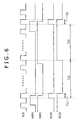
- the vertical clock VCK is given to the write scanning circuit 4 as well as to the duty scanning drive circuit 5 shown in Fig. 1. Further the start pulse VSP1 is given to the write scanning drive circuit 4, and the vertical start pulse VSP2 is given to the duty scanning drive circuit 5.
- Each of the write scanning circuit 4 and duty scanning drive circuit 5 incorporates a shift register, and transfers the vertical start pulses VSP1 and VSP2 according to the timing of the vertical clock VCK to a shift register in the next stage.
- each of the signals SC1X and SC2X is indicates a pulse based on the vertical start pulses VSP1 and VSP2 respectively, outputted from the sift register in one stage of the write scanning line X and the duty scanning line Z in synchronism to the vertical clock VCK.
- both the signals SC1X and SC2X go to the H (High) level during the period of T11, and the N type write scanning transistor 15 and duty control transistor 17 in Fig. 3 are turned ON simultaneously.
- a gate of the drive transistor 16 is connected to the data line Y, and a drain of the drive transistor 16 is connected to an anode of the organic EL element 13.
- a voltage corresponding to data brightness is given via the data line Y to the drive transistor 16
- a current corresponding to the data line voltage is given via the current supply line 14 to the organic EL element 13 through voltage current conversion by the drive transistor 16.
- the organic EL element 13 emits light with intensity corresponding to the drive current.
- This period of time T11 is described hereinafter as write period.
- the N type write scanning transistor 15 goes OFF, and the data line Y is disconnected from the gate of the drive transistor 16.
- the gate of the drive transistor 16 is maintained at the same voltage by the storage capacity 18. Namely, the voltage given during the write period T11 is maintained. Further as the duty control transistor 17 is ON, also the drive current given in the write period T11 is maintained, so that the illumination intensity of the organic EL element is maintained.
- both of the signals SC1X and SC2X go high, and the write period T11 is restarted. So the period of time T13 from the end of the light ON period T12 until start of the next write period T11 is described as light OFF period.
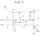
- Fig. 5 shows another example of configuration of the pixel 12 in the organic EL display section 2, and shows a current write type of pixel circuit 12B which writes brightness information by controlling a current for the data line Y.
- This pixel circuit 12B includes an organic EL element 13, a current supply line 14, a data line Y, a write scanning line X, a duty scanning line Z, an N type of write scanning transistor 19, a P type of drive transistor 20, a P type of write transistor 21, an N type of delete scanning transistor 22, and a storage capacity 23.
- a source (or a drain) of the write scanning transistor 19 is connected to a drain of the write transistor 21, and a drain (or a source) thereof is connected to the data line Y.
- Connected to a gate of the write scanning transistor 19 is the write scanning line X.
- a gate and a drain of the write transistor 21 are short-circuited, and the source is connected to the current supply line 14.
- a source (or a drain) of the delete scanning transistor 22 is connected to a gate of the write transistor 21, and the drain (or a source) is connected to a gate of the drive transistor 20.
- Connected to a gate of the delete scanning transistor 22 is the duty scanning line Z.
- a source of the drive transistor 20 is connected to the current supply line 14, and a drain thereof is connected to an anode of the organic EL element 13. Further one terminal of the storage capacity 23 is connected to a gate of the drive transistor 20, and another terminal thereof is connected to the current supply line 14.
- the write scanning transistor 19 and write transistor 21 correspond to the "active element for write scanning” and the drive transistor 20 corresponds to the “active element for driving” in the present invention. Further the delete scanning transistor 22 corresponds to the "active element for lighting out” in the present invention.
- the write scanning transistor 19 and the delete scanning transistor 22 are N-type transistors, but either one or both of the transistors may be a P-type transistor or P-type transistors.
- both the signals SC1X and SC2X go to an H level, and the write scanning transistor 19 and the delete scanning transistor 22 shown in Fig. 5 are turned ON simultaneously.
- a drain of the write transistor 21 is connected to the data line Y, and during this period of time T21, a current corresponding to the data brightness is fetched from the data line Y and is converted to a voltage by the write transistor 21 and is stored in the storage capacity 23.
- a current corresponding to the voltage stored in the storage capacity 23 is supplied from the current supply line 14 to the organic EL element 13.
- This period of time T21 is described as a write period below.
- the write scanning transistor 19 and the delete scanning transistor 22 are turned OFF simultaneously.
- a voltage at a gate of the drive transistor 20 is maintained by the storage capacity 23. Namely the voltage given in the period of time T21 is maintained. Also the drive current given in the period of time T21 is maintained, and the illuminance intensity of the organic El element is maintained.
- a light-emitting operation of the organic EL element 13 is performed by the pixel circuit 12A (or 12B) pixel by pixel in response to selection scanning for the write scanning line X by the write scanning drive circuit 4 and selection driving by the data line drive circuit 3 via the data line Y.
- a screen corresponding to the brightness information from the data line drive circuit 3 is driven for displaying with a predetermined scanning cycle in the organic EL display section 2.
- the organic EL active matrix type of display unit 1 has a function for adjusting display brightness of the screen according to brightness of the environment for use thereof.
- the screen brightness adjusting mechanism according to the present invention is described below.
- the illuminance detector 9 includes an illuminance sensor 10 including a light receiving sensor or the like and a resistor 11, and is provided, for instance, at a position close to the organic EL display section 2 on the same plane as the organic EL display section 2.
- the illuminance sensor 10 generates a proportional amount of current to the intensity (brightness) of external light with the photoelectric conversion effect.
- the current generated by the illuminance sensor 10 is converted to a voltage signal by the resistor 11 and then supplied to the calculating section 8.
- Supply of an output from the illuminance detector 9 to the calculating section 8 is performed, for instance, in synchronism to a scanning cycle of the write scanning line X.
- the calculating section 8 includes, for instance, an A/D converter, and digitalizes a terminal voltage between the illuminance sensor 10 and the resistor 11 with this A/D converter. Further the calculating section 8 has a calculating mechanism for calculating the brightness corresponding to the value digitalized by the A/D converter, and supplies a brightness set value calculated by this calculating mechanism to the scanning control drive section 7.
- the scanning control drive section 7 supplies, as described above, a vertical clock VCK and a vertical start pulse VSP1 to the write scanning drive circuit 4 and executes selection scanning for the write scanning line X.
- the scanning control drive section 7, write scanning drive circuit 4, and duty scanning drive circuit 5 composes the "scanning drive unit" according to the present invention, and drives screen displays on the organic EL display section 2 together with the "data drive unit” formed with the data control drive section 6 and data line drive circuit 3.
- the data control drive section 6 and scanning control drive section 7 may be formed in the same IC.
- the scanning control drive section 7 supplies the vertical clock VCK and vertical start pulse VSP2 to the duty scanning drive circuit 5 as described above to control a light emission period of time for the organic EL element 13 of each pixel within one scanning cycle.
- the light emission period of time of the organic EL element 13 is adjusted according to a result of detection by the illuminance detector 9. Namely, when the ambient environment is bright, light emission of the organic EL element 13 is continued for a relatively long period of time enabling acquisition of a large brightness set value, and when the ambient environment is dark, light emission of the organic EL element 13 is conducted for a relatively short period of time for achieving a small brightness set value.
- the brightness set value calculated by the calculating section 8 based on brightness of an ambient environment detected by the illuminance detector 9 is used as a control parameter for deciding a light emission period of time for the organic EL element 13.
- the scanning control drive section 7 converts a brightness set value supplied from the calculating section 8 to a pulse and supplies the pulse as a control signal to the duty scanning drive circuit 5 to adjust the average brightness of a screen within one scanning cycle for obtaining the screen brightness corresponding to the ambient environment.
- the brightness set value is not always calculated based on an output from the illuminance detector 9 and through a predetermined arithmetic expression, and also the configuration is allowable in which a correspondence table between brightness set values and output values from the illuminance detector 9 may be previously stored and a brightness set value suited to the current ambient environment may be selected.
- adjustment of the light emission period of time of the organic EL element 13 can be performed by controlling the timing for stopping light emission given by the duty scanning drive circuit 5, namely by controlling the timing for driving of the duty control transistor 17 (Fig. 3) or delete scanning transistor 22, (Fig. 5). Adjustment of a light transmission period of time of the organic EL element 13 can be performed also by controlling the timing for start of light emission given by the write scanning drive circuit 4, namely by controlling the timing for driving of the write scanning transistors 15, 19.
- the calculating section 8, scanning control drive section 7, write scanning drive circuit 4, and duty scanning drive circuit 5 form the "control unit" in the present invention.
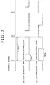
- Fig. 7 shows an example of a control signal supplied from the scanning control drive section 7 to the duty scanning drive circuit 5.
- the organic EL element 13 used in the present invention is designed, for instance, so that, when the light emission period of time for one field period (16.67 ms) is 100% of the duty ratio, the average brightness for about 100 cd/m2 is obtained for a light emission period of time equivalent to 25% of the duty ratio (4.167 ms), or the average brightness of about 200 cd/m2 for a light emission period of time equivalent to 50% of the duty ratio (8.33 ms).
- the light emission period of time namely the light ON period of time (T12, T22) is controlled, as described above, according to the output timing for a signal SC2X supplied from the duty scanning drive circuit 5 to each pixel 12. Therefore, the control signal can be configured as the vertical start pulse VSP2 for adjusting an output of the signal SC2X so that the light emission period of time corresponding to the brightness set value calculated by the calculating section 8 can be obtained.
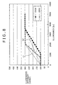
- Fig. 8 shows an example of control over the illuminance of the organic EL element 13 corresponding to the illuminance of an ambient environment detected by the illuminance detector 9.
- light emission period of time of the organic EL element 13 is controlled in response to brightness of external light, and in this step, the light emission period of time of the organic EL element 13 is controlled so that the display brightness satisfying the target screen contrast such as the contrast ratio of 30 or 50 can be obtained. Because of this feature, the visibility of the screen can be secured with unnecessary increase in power consumption suppressed.
- a maximum value and a minimum value for the illumination intensity are set for defining a range for adjustment of the brightness for the purpose to prevent the screen brightness from being too bright or too dark.
- the minimum value for the illuminance intensity of the organic EL element 13 is set to 100 cd/m2 (25% of the duty ratio), and the maximum value to 300 cd/m2 (75% of the duty ratio), and the light emission period of time of the organic EL element 13 is controlled so that a predetermined screen contrast can be obtained in this range.
- the target screen contrast is not always required to be constant. It is required only that the satisfying screen contrast can be obtained within the range for adjustment of the illumination intensity.
- the dash and dot line L1 indicates a case of control in the case where the target screen contrast is 50% of duty ratio
- the chain double-dashed line L2 indicates a case in which the target screen contrast is 30% of duty ratio.
- brightness of a screen display can be adjusted in response to brightness of the ambient environment by controlling a light emission period of time of the organic EL element 13 within one scanning cycle for each pixel 12, so that the brightness of the screen display can easily and smoothly be performed.
- a control signal independent from brightness information for the data line Y provided by the data control drive section 6 and data line drive circuit 3 is generated in the calculating section 8, and the control signal is supplied via the scanning control drive section 7 to the duty scanning drive circuit 5 to adjust brightness of each pixel, so that, even when brightness of a display is rather low, the dynamic range is not narrowed and degradation of image quality due to noises or non-uniformity of performances of elements never occurs, which ensures high quality screen display.
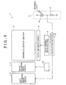
- a brightness set value calculated in the calculating section 8 is supplied via the scanning control drive section 7 to the duty scanning drive circuit 5, but for instance, as shown in Fig. 9, the brightness set value calculated in the calculating section 8 may directly be supplied to the duty scanning drive circuit 5.
- supply of a vertical clock or a vertical start pulse to the write scanning drive circuit 4 is executed by a write scanning control drive section 25 separately.
- the active matrix type of display apparatus was described by referring to a display device using an organic EL element, but the present invention is not limited to this configuration, and is applicable also to a display device using other types of self-luminous elements such as a light emitting diode (LED).
- LED light emitting diode
Landscapes
- Engineering & Computer Science (AREA)
- Physics & Mathematics (AREA)
- Computer Hardware Design (AREA)
- General Physics & Mathematics (AREA)
- Theoretical Computer Science (AREA)
- Electroluminescent Light Sources (AREA)
- Control Of Indicators Other Than Cathode Ray Tubes (AREA)
- Control Of El Displays (AREA)
- Devices For Indicating Variable Information By Combining Individual Elements (AREA)
Applications Claiming Priority (2)
| Application Number | Priority Date | Filing Date | Title |
|---|---|---|---|
| JP2004122628A JP2005308857A (ja) | 2004-04-19 | 2004-04-19 | アクティブマトリクス型表示装置およびその駆動方法 |
| JP2004122628 | 2004-04-19 |
Publications (2)
| Publication Number | Publication Date |
|---|---|
| EP1589518A2 true EP1589518A2 (de) | 2005-10-26 |
| EP1589518A3 EP1589518A3 (de) | 2006-07-05 |
Family
ID=34942163
Family Applications (1)
| Application Number | Title | Priority Date | Filing Date |
|---|---|---|---|
| EP05290864A Withdrawn EP1589518A3 (de) | 2004-04-19 | 2005-04-19 | Aktivmatrixanzeigevorrichtung und Steuerungsverfahren dafür |
Country Status (6)
| Country | Link |
|---|---|
| US (1) | US20050253835A1 (de) |
| EP (1) | EP1589518A3 (de) |
| JP (1) | JP2005308857A (de) |
| KR (1) | KR20060046635A (de) |
| CN (1) | CN100399395C (de) |
| TW (1) | TW200625241A (de) |
Cited By (4)
| Publication number | Priority date | Publication date | Assignee | Title |
|---|---|---|---|---|
| EP1939594A3 (de) * | 2006-12-27 | 2009-11-04 | Samsung SDI Co., Ltd. | Umgebungslichterfassungsschaltung und Flachbildanzeige mit Umgebungslichterfassungsschaltung |
| WO2011117684A1 (en) | 2010-03-25 | 2011-09-29 | Nokia Corporation | Method and apparatus for reducing flickering and motion blur in a display device |
| US8564579B2 (en) | 2006-12-27 | 2013-10-22 | Samsung Display Co., Ltd. | Ambient light sensing circuit and flat panel display including ambient light sensing circuit |
| CN109983530A (zh) * | 2016-12-22 | 2019-07-05 | 杜比实验室特许公司 | 环境光自适应显示管理 |
Families Citing this family (39)
| Publication number | Priority date | Publication date | Assignee | Title |
|---|---|---|---|---|
| KR100782456B1 (ko) * | 2005-04-29 | 2007-12-05 | 삼성에스디아이 주식회사 | 유기 전계발광 표시장치의 구동 방법 |
| CN100592358C (zh) * | 2005-05-20 | 2010-02-24 | 株式会社半导体能源研究所 | 显示装置和电子设备 |
| KR100646993B1 (ko) * | 2005-09-15 | 2006-11-23 | 엘지전자 주식회사 | 유기 전계 발광 소자 및 그 구동방법 |
| JP4899447B2 (ja) | 2005-11-25 | 2012-03-21 | ソニー株式会社 | 自発光表示装置、発光条件制御装置、発光条件制御方法及びプログラム |
| US7515822B2 (en) * | 2006-05-12 | 2009-04-07 | Microsoft Corporation | Imaging systems' direct illumination level adjusting method and system involves adjusting operation of image sensor of imaging system based on detected level of ambient illumination |
| JP5050462B2 (ja) * | 2006-09-15 | 2012-10-17 | ソニー株式会社 | 焼き付き抑制装置、自発光表示装置、画像処理装置、電子機器、焼き付き抑制方法及びコンピュータプログラム |
| KR100804529B1 (ko) * | 2006-09-18 | 2008-02-20 | 삼성에스디아이 주식회사 | 유기 발광 디스플레이 장치 및 그의 구동 방법 |
| KR100781651B1 (ko) * | 2006-11-06 | 2007-12-03 | 삼성전자주식회사 | 휴대용 단말기의 화면 표시 장치 및 방법 |
| JP2008139520A (ja) * | 2006-12-01 | 2008-06-19 | Sony Corp | 表示装置 |
| KR100857672B1 (ko) | 2007-02-02 | 2008-09-08 | 삼성에스디아이 주식회사 | 유기전계발광표시장치 및 그의 구동방법 |
| KR100836425B1 (ko) | 2007-02-05 | 2008-06-09 | 삼성에스디아이 주식회사 | 유기 전계 발광표시장치 및 그 구동방법 |
| KR100836433B1 (ko) | 2007-02-05 | 2008-06-09 | 삼성에스디아이 주식회사 | 유기 전계 발광표시장치 및 그 구동방법 |
| KR100836438B1 (ko) * | 2007-02-05 | 2008-06-09 | 삼성에스디아이 주식회사 | 유기 전계 발광표시장치 및 그 구동방법 |
| KR100836423B1 (ko) | 2007-02-05 | 2008-06-09 | 삼성에스디아이 주식회사 | 유기 전계 발광표시장치 및 그 구동방법 |
| KR100836432B1 (ko) | 2007-02-05 | 2008-06-09 | 삼성에스디아이 주식회사 | 유기 전계 발광표시장치 및 그 구동방법 |
| KR100840102B1 (ko) | 2007-02-23 | 2008-06-19 | 삼성에스디아이 주식회사 | 유기 전계발광 표시장치 |
| KR100858614B1 (ko) | 2007-03-08 | 2008-09-17 | 삼성에스디아이 주식회사 | 유기전계발광표시장치 및 그의 구동방법 |
| US8994757B2 (en) * | 2007-03-15 | 2015-03-31 | Scalable Display Technologies, Inc. | System and method for providing improved display quality by display adjustment and image processing using optical feedback |
| KR20080086747A (ko) | 2007-03-23 | 2008-09-26 | 삼성에스디아이 주식회사 | 유기 전계 발광 표시 장치 및 그 구동 방법 |
| CN101681591B (zh) * | 2007-05-25 | 2012-07-18 | 索尼株式会社 | 显示设备及影像信号处理方法 |
| JP4462293B2 (ja) * | 2007-06-01 | 2010-05-12 | エプソンイメージングデバイス株式会社 | 液晶表示装置、電子機器及び前記液晶表示装置の照光手段の明るさを制御する方法 |
| BRPI0813523A2 (pt) * | 2007-07-11 | 2014-12-23 | Sony Corp | Dispositivo de exibição, método e processamento de sinal de imagem de um dispositivo de exibição, e, programa. |
| JP2010072112A (ja) * | 2008-09-16 | 2010-04-02 | Casio Computer Co Ltd | 表示装置及びその駆動制御方法 |
| KR101056231B1 (ko) | 2009-03-27 | 2011-08-11 | 삼성모바일디스플레이주식회사 | 유기전계발광표시장치 |
| CN102421216B (zh) * | 2010-09-28 | 2014-05-07 | 深圳市长运通光电技术有限公司 | 一种led阵列扫描芯片、led设备及led扫描电路 |
| CN102568438A (zh) * | 2010-12-13 | 2012-07-11 | 周锡卫 | 显示装置自适应亮度智能调节器及实现方法 |
| CN102800274B (zh) * | 2011-05-26 | 2015-03-25 | 群康科技(深圳)有限公司 | 显示装置及其控制方法 |
| US9053665B2 (en) | 2011-05-26 | 2015-06-09 | Innocom Technology (Shenzhen) Co., Ltd. | Display device and control method thereof without flicker issues |
| US9747834B2 (en) * | 2012-05-11 | 2017-08-29 | Ignis Innovation Inc. | Pixel circuits including feedback capacitors and reset capacitors, and display systems therefore |
| JP5423859B2 (ja) * | 2012-10-15 | 2014-02-19 | ソニー株式会社 | 自発光型表示装置およびその駆動方法 |
| US9940873B2 (en) * | 2014-11-07 | 2018-04-10 | Apple Inc. | Organic light-emitting diode display with luminance control |
| US10186187B2 (en) | 2015-03-16 | 2019-01-22 | Apple Inc. | Organic light-emitting diode display with pulse-width-modulated brightness control |
| KR102247526B1 (ko) | 2015-07-10 | 2021-05-03 | 삼성전자주식회사 | 디스플레이 장치 및 그 제어 방법 |
| JP2017049367A (ja) * | 2015-08-31 | 2017-03-09 | シャープ株式会社 | 表示装置および電子機器 |
| JP6828247B2 (ja) | 2016-02-19 | 2021-02-10 | セイコーエプソン株式会社 | 表示装置及び電子機器 |
| CN113936601A (zh) * | 2016-04-22 | 2022-01-14 | 索尼公司 | 显示装置与电子设备 |
| KR102573340B1 (ko) | 2016-10-25 | 2023-09-01 | 엘지디스플레이 주식회사 | 유기발광표시장치 및 그 구동장치 |
| JP2018155832A (ja) | 2017-03-16 | 2018-10-04 | セイコーエプソン株式会社 | 電気光学装置、電子機器及び電気光学装置の駆動方法 |
| CN115620667B (zh) * | 2022-12-19 | 2023-03-10 | 惠科股份有限公司 | 显示装置和显示方法 |
Citations (4)
| Publication number | Priority date | Publication date | Assignee | Title |
|---|---|---|---|---|
| EP1102234A2 (de) | 1999-11-18 | 2001-05-23 | Sony Corporation | Anzeigeeinrichtung mit aktiver Matrix und Treiberschaltung dafür |
| EP1164641A2 (de) | 2000-06-12 | 2001-12-19 | Semiconductor Energy Laboratory Co., Ltd. | Lichtemittierendes Modul, Verfahren zu seiner Ansteuerung und optischer Sensor |
| US20030067424A1 (en) | 2001-10-10 | 2003-04-10 | Hajime Akimoto | Image display device |
| US20040012340A1 (en) | 2002-04-03 | 2004-01-22 | Sanyo Electric Co., Ltd. | Organic EL display device |
Family Cites Families (21)
| Publication number | Priority date | Publication date | Assignee | Title |
|---|---|---|---|---|
| US5952789A (en) * | 1997-04-14 | 1999-09-14 | Sarnoff Corporation | Active matrix organic light emitting diode (amoled) display pixel structure and data load/illuminate circuit therefor |
| US6147664A (en) * | 1997-08-29 | 2000-11-14 | Candescent Technologies Corporation | Controlling the brightness of an FED device using PWM on the row side and AM on the column side |
| US6337675B1 (en) * | 1997-10-30 | 2002-01-08 | Ut Automotive Dearborn, Inc | Display system with automatic and manual brightness control |
| JP4092857B2 (ja) * | 1999-06-17 | 2008-05-28 | ソニー株式会社 | 画像表示装置 |
| TWI252592B (en) * | 2000-01-17 | 2006-04-01 | Semiconductor Energy Lab | EL display device |
| JP2003527630A (ja) * | 2000-03-14 | 2003-09-16 | コーニンクレッカ フィリップス エレクトロニクス エヌ ヴィ | 経時及び周囲光に依存して輝度補正するエレクトロルミネッセント表示装置 |
| JP2002162934A (ja) * | 2000-09-29 | 2002-06-07 | Eastman Kodak Co | 発光フィードバックのフラットパネルディスプレイ |
| US6580657B2 (en) * | 2001-01-04 | 2003-06-17 | International Business Machines Corporation | Low-power organic light emitting diode pixel circuit |
| US7227517B2 (en) * | 2001-08-23 | 2007-06-05 | Seiko Epson Corporation | Electronic device driving method, electronic device, semiconductor integrated circuit, and electronic apparatus |
| JP2003108073A (ja) * | 2001-09-28 | 2003-04-11 | Toshiba Corp | 自己発光型表示装置 |
| JP2003108075A (ja) * | 2001-09-29 | 2003-04-11 | Toshiba Corp | 表示装置およびその駆動方法 |
| JP2003122305A (ja) * | 2001-10-10 | 2003-04-25 | Sony Corp | 有機el表示装置およびその制御方法 |
| JP2003131619A (ja) * | 2001-10-25 | 2003-05-09 | Toshiba Corp | 自己発光型表示装置 |
| JP4293747B2 (ja) * | 2001-12-26 | 2009-07-08 | ソニー株式会社 | 有機el表示装置およびその制御方法 |
| JP3724430B2 (ja) * | 2002-02-04 | 2005-12-07 | ソニー株式会社 | 有機el表示装置およびその制御方法 |
| JP2003308046A (ja) * | 2002-02-18 | 2003-10-31 | Sanyo Electric Co Ltd | 表示装置 |
| US6841947B2 (en) * | 2002-05-14 | 2005-01-11 | Garmin At, Inc. | Systems and methods for controlling brightness of an avionics display |
| JP4593868B2 (ja) * | 2002-05-14 | 2010-12-08 | ソニー株式会社 | 表示装置およびその駆動方法 |
| JP2003330383A (ja) * | 2002-05-17 | 2003-11-19 | Sony Corp | 有機el表示装置 |
| JP4099572B2 (ja) * | 2002-05-20 | 2008-06-11 | ソニー株式会社 | 有機el表示装置 |
| US20050212824A1 (en) * | 2004-03-25 | 2005-09-29 | Marcinkiewicz Walter M | Dynamic display control of a portable electronic device display |
-
2004
- 2004-04-19 JP JP2004122628A patent/JP2005308857A/ja active Pending
-
2005
- 2005-04-07 US US11/100,481 patent/US20050253835A1/en not_active Abandoned
- 2005-04-08 KR KR1020050029363A patent/KR20060046635A/ko not_active Withdrawn
- 2005-04-11 TW TW094111410A patent/TW200625241A/zh unknown
- 2005-04-19 CN CNB2005100672194A patent/CN100399395C/zh not_active Expired - Fee Related
- 2005-04-19 EP EP05290864A patent/EP1589518A3/de not_active Withdrawn
Patent Citations (4)
| Publication number | Priority date | Publication date | Assignee | Title |
|---|---|---|---|---|
| EP1102234A2 (de) | 1999-11-18 | 2001-05-23 | Sony Corporation | Anzeigeeinrichtung mit aktiver Matrix und Treiberschaltung dafür |
| EP1164641A2 (de) | 2000-06-12 | 2001-12-19 | Semiconductor Energy Laboratory Co., Ltd. | Lichtemittierendes Modul, Verfahren zu seiner Ansteuerung und optischer Sensor |
| US20030067424A1 (en) | 2001-10-10 | 2003-04-10 | Hajime Akimoto | Image display device |
| US20040012340A1 (en) | 2002-04-03 | 2004-01-22 | Sanyo Electric Co., Ltd. | Organic EL display device |
Cited By (8)
| Publication number | Priority date | Publication date | Assignee | Title |
|---|---|---|---|---|
| EP1939594A3 (de) * | 2006-12-27 | 2009-11-04 | Samsung SDI Co., Ltd. | Umgebungslichterfassungsschaltung und Flachbildanzeige mit Umgebungslichterfassungsschaltung |
| US7859486B2 (en) | 2006-12-27 | 2010-12-28 | Samsung Mobile Display Co., Ltd. | Ambient light sensing circuit and flat panel display including ambient light sensing circuit |
| US8564579B2 (en) | 2006-12-27 | 2013-10-22 | Samsung Display Co., Ltd. | Ambient light sensing circuit and flat panel display including ambient light sensing circuit |
| WO2011117684A1 (en) | 2010-03-25 | 2011-09-29 | Nokia Corporation | Method and apparatus for reducing flickering and motion blur in a display device |
| EP2548196A4 (de) * | 2010-03-25 | 2014-02-26 | Nokia Corp | Verfahren und vorrichtung zur reduzierung des flimmern und der bewegungsunschärfe in einer anzeigevorrichtung |
| US9142188B2 (en) | 2010-03-25 | 2015-09-22 | Nokia Technologies Oy | Methods and apparatus for reducing flickering and motion blur in a display device |
| US10991338B2 (en) | 2010-03-25 | 2021-04-27 | Nokia Technologies Oy | Apparatus, display module and method for adaptive blank frame insertion |
| CN109983530A (zh) * | 2016-12-22 | 2019-07-05 | 杜比实验室特许公司 | 环境光自适应显示管理 |
Also Published As
| Publication number | Publication date |
|---|---|
| TW200625241A (en) | 2006-07-16 |
| CN1691112A (zh) | 2005-11-02 |
| CN100399395C (zh) | 2008-07-02 |
| US20050253835A1 (en) | 2005-11-17 |
| KR20060046635A (ko) | 2006-05-17 |
| JP2005308857A (ja) | 2005-11-04 |
| EP1589518A3 (de) | 2006-07-05 |
Similar Documents
| Publication | Publication Date | Title |
|---|---|---|
| EP1589518A2 (de) | Aktivmatrixanzeigevorrichtung und Steuerungsverfahren dafür | |
| CN103021335B (zh) | 一种oled驱动电路、oled显示装置及其亮度调节的方法 | |
| US10665165B2 (en) | Organic light-emitting display panel, organic light-emitting display apparatus, and driving method of organic light-emitting display panel | |
| CN100578582C (zh) | 残影减少设备及方法、自发光显示设备及图像处理设备 | |
| TWI389077B (zh) | 有機發光二極體顯示裝置及其驅動方法 | |
| US7773080B2 (en) | Display device and the driving method which restricts electric power | |
| JP4352893B2 (ja) | 電子装置の駆動方法、電子装置、半導体集積回路及び電子機器 | |
| KR101346925B1 (ko) | 표시 장치, 그 구동 방법 및 전자 기기 | |
| TWI395197B (zh) | 特徵強調控制裝置,顯示設備,特徵強調設備,處理器及電腦程式產品 | |
| CN115376459A (zh) | 显示设备 | |
| CN111599295B (zh) | 显示装置及其峰值亮度控制方法 | |
| US20080001974A1 (en) | Organic light emitting diode display and driving method thereof | |
| US8217865B2 (en) | Display apparatus and driving method for the same | |
| CN101393719A (zh) | 显示装置、显示驱动方法 | |
| JP2012098707A (ja) | 表示装置及びその駆動方法 | |
| US7839361B2 (en) | Method of driving organic light emitting display | |
| JP2006047617A (ja) | エレクトロルミネセンス表示装置およびその駆動方法 | |
| JP5239773B2 (ja) | 表示装置 | |
| US20080117196A1 (en) | Display device and driving method thereof | |
| JP2008185670A (ja) | 有機el表示装置、有機el表示装置の制御方法および電子機器 | |
| JP2005062485A (ja) | 有機el表示装置およびその駆動方法 | |
| JP5228823B2 (ja) | 表示装置 | |
| TWI399723B (zh) | 顯示裝置,顯示裝置之驅動方法及電子裝置 | |
| JP2012093434A (ja) | 表示装置の駆動方法 | |
| JP2006038966A (ja) | 画像表示装置及びその駆動方法 |
Legal Events
| Date | Code | Title | Description |
|---|---|---|---|
| PUAI | Public reference made under article 153(3) epc to a published international application that has entered the european phase |
Free format text: ORIGINAL CODE: 0009012 |
|
| AK | Designated contracting states |
Kind code of ref document: A2 Designated state(s): AT BE BG CH CY CZ DE DK EE ES FI FR GB GR HU IE IS IT LI LT LU MC NL PL PT RO SE SI SK TR |
|
| AX | Request for extension of the european patent |
Extension state: AL BA HR LV MK YU |
|
| PUAL | Search report despatched |
Free format text: ORIGINAL CODE: 0009013 |
|
| AK | Designated contracting states |
Kind code of ref document: A3 Designated state(s): AT BE BG CH CY CZ DE DK EE ES FI FR GB GR HU IE IS IT LI LT LU MC NL PL PT RO SE SI SK TR |
|
| AX | Request for extension of the european patent |
Extension state: AL BA HR LV MK YU |
|
| 17P | Request for examination filed |
Effective date: 20061212 |
|
| AKX | Designation fees paid |
Designated state(s): AT BE BG CH CY CZ DE DK EE ES FI FR GB GR HU IE IS IT LI LT LU MC NL PL PT RO SE SI SK TR |
|
| 17Q | First examination report despatched |
Effective date: 20080730 |
|
| STAA | Information on the status of an ep patent application or granted ep patent |
Free format text: STATUS: THE APPLICATION IS DEEMED TO BE WITHDRAWN |
|
| 18D | Application deemed to be withdrawn |
Effective date: 20100806 |