EP1586183B1 - Ensemble oscillateur utilise a des fins de modulation de frequence - Google Patents
Ensemble oscillateur utilise a des fins de modulation de frequence Download PDFInfo
- Publication number
- EP1586183B1 EP1586183B1 EP03782441A EP03782441A EP1586183B1 EP 1586183 B1 EP1586183 B1 EP 1586183B1 EP 03782441 A EP03782441 A EP 03782441A EP 03782441 A EP03782441 A EP 03782441A EP 1586183 B1 EP1586183 B1 EP 1586183B1
- Authority
- EP
- European Patent Office
- Prior art keywords
- oscillator
- current
- frequency
- input
- output
- Prior art date
- Legal status (The legal status is an assumption and is not a legal conclusion. Google has not performed a legal analysis and makes no representation as to the accuracy of the status listed.)
- Expired - Fee Related
Links
Images

Classifications
-
- H—ELECTRICITY
- H04—ELECTRIC COMMUNICATION TECHNIQUE
- H04L—TRANSMISSION OF DIGITAL INFORMATION, e.g. TELEGRAPHIC COMMUNICATION
- H04L27/00—Modulated-carrier systems
- H04L27/10—Frequency-modulated carrier systems, i.e. using frequency-shift keying
- H04L27/12—Modulator circuits; Transmitter circuits
Definitions
- the present invention relates to an oscillator arrangement designed for frequency modulation.
- Frequency Shift Keying in addition to amplitude shift keying and phase shift keying, as well as combinations of these methods, is a common method for digital modulation of a carrier signal.
- One way to apply a carrier to frequency shift keying is to modulate the carrier signal as it is being generated in the oscillator.
- the frequency shift keying of the oscillator is usually achieved by adding or disconnecting small, frequency-determining capacitances to a resonant circuit formed in the oscillator.
- the digital modulation signal is modulated onto the carrier with the desired frequency deviation.
- the oscillator can be embodied for example as a quartz oscillator or as an LC oscillator. While in a quartz oscillator, the oscillation frequency is mainly determined by the oscillation frequency of the quartz, at least one inductance and at least one capacitance influence the oscillation frequency in the case of the LC oscillator.
- the document US 2,874,216 relates to an automatic signal control system.
- the object of the present invention is to provide an oscillator arrangement which is suitable for a modulation according to a frequency shift keying method and in which problems caused by charge injection are avoided or significantly reduced.
- the automatic amplitude control which is usually present anyway in a controlled oscillator with frequency modulation, is also used to control the operating current of the oscillator and so that the oscillator frequency in the desired manner to influence, that is to modulate.
- the oscillator is thus modulated by the loop gain of the gain control loop is controlled by influencing the supply current of the oscillator.
- the amplitude control loop is used to change the so-called base current of the oscillator by means of the modulation signal controlled Stromabzugstechnik and thus to change the frequency in small steps.
- the proposed principle is advantageously applicable, inter alia, both in LC oscillators and quartz oscillators.
- the means for influencing the supply current preferably comprises a plurality of current switches connected in parallel with respect to their connected paths. Depending on the modulation signal, the parallel-connected current switches are preferably controlled so that just the current required for the desired frequency detuning current is subtracted.
- the parallel-connected current switches are preferably arranged on the output side in a current mirror.
- each one transistor of the current mirror and a switch associated therewith form a series circuit.
- the series circuits are connected in parallel to each other.
- the switches can be switched on and off independently of each other.
- the current mirror with the parallel-connected current switches preferably acts on a further current mirror, which couples a supply current source for supplying the oscillator with the oscillator.
- the circuit node at which the current mirror engages with the current switches in the supply current supply of the oscillator is preferably provided at the common gate terminal or base terminal of the current mirror transistors in the further current mirror.
- a control block is preferably provided with an input to which the modulation signal is supplied and with one or more outputs which are connected to respective control terminals of the associated power switch.
- the modulation signal is preferably a digitally coded signal, which is coded according to a frequency shift keying method, FSK.
- the oscillator is preferably designed to be tunable with a further control input, to which a tuning signal can be fed and with an oscillation frequency-determining capacitor, which is controlled in dependence on the tuning signal.
- Such tunable capacitances are preferably designed as varactor diodes.
- FIG. 1 shows an oscillator arrangement designed for frequency modulation. This comprises an oscillator 1 and a control input 2 for supplying a modulation signal.
- the oscillator 1 has an output 3 to which a frequency modulated signal can be tapped.
- the oscillator 1 has an input 4 for supplying a supply current.
- the supply current is used, inter alia, for the damping of the resonant circuit, which is formed in the oscillator 1.
- the supply current is also referred to as base current or tail current. To ensure the stability of the oscillator, this is arranged in an amplitude control loop.
- the control circuit for amplitude control comprises an AGC block 5, a first current mirror 6 and a second current mirror 7, 8.
- the output of the first current mirror 6 controls a Stromettintransistor 7, which at its current source output to the supply current input 4 of the oscillator. 1 connected is.
- a transistor diode 8 forms with the current source transistor 7, the second current mirror.
- the common gate terminal of the transistors 7, 8, which is connected to the output of the first current mirror 6, is referred to as circuit node K.
- the input of the second current mirror 7, 8 is connected to a current source 9, which provides a reference current for the oscillator 1.
- the current mirror 6 comprises a transistor diode M1 and the output side a total of four parallel-connected current mirror transistors M2, M3, M4, M5, which are independently switched on and off.
- a respective switch 10, 11, 12, 13 is provided, each of which connects a reference potential terminal 14 to a load terminal of the controlled paths of the associated transistor M2, M3, M4, M5, in this case with their source terminal.
- the gate terminals of the field effect transistors M1 to M5 in the current mirror 6 are connected directly to one another.
- the transistor M1 In order for the transistor M1 to operate as a diode, its gate terminal is directly connected to its drain terminal.
- the source terminal of the n-channel field effect transistor M1 is connected to the reference potential terminal 14.
- the drain terminals of the transistors M2 to M5 are directly connected together in the circuit node K and form the output of the current mirror 6.
- the circuit node K is connected directly to the gate terminals of the current mirror transistors 7, 8.
- the switches 10, 11, 12, 13, which are designed as a current switch, are controlled by a control logic which is provided in a corresponding control block 15, whose input forms the control input 2 for supplying a modulation signal of the oscillator arrangement and whose output to the control terminals of Switch 10, 11, 12, 13 is connected.
- a possibly existing tuning input of the voltage-controlled oscillator 1 is not shown in FIG.
- the peculiarity of the circuit according to FIG. 1 is that the modulation data does not control switchable capacitors provided directly in the oscillator core, which thus influence the oscillation frequency of the oscillator, but that the modulation data intervene in the amplitude regulation of the oscillator 1.
- the oscillator frequency is indirectly keyed over the control of the supply current of the oscillator, English tail current.
- the amplitude control circuit 5, 6, 7 comprises switchable current mirror, with which the frequency of the oscillator can be adjusted.
- the modulation signal thus controls the loop gain of the amplitude control loop 5, 6, 7.
- With the power switches frequency conversion of the oscillator 1 is realized in a Stromabzugstechnik.
- FIG. 2 shows a further exemplary embodiment of the present oscillator arrangement, which has an oscillator realized as quartz oscillator 1 '.
- the amplitude control including the switchable current sources in the amplitude control loop and their control with the modulation signal correspond to those of Figure 1.
- the oscillator 1 'in Figure 2 is designed as a quartz oscillator and comprises a quartz crystal 16. Both terminals of the quartz oscillator 16 are connected via a respective capacitor 17, 18 with reference potential.
- an amplifier is provided which comprises a p-channel field effect transistor 19.
- the gate terminal of the transistor 19, at the same time the output 3 of the oscillator is formed, is connected to one of the two terminals of the quartz 16.
- the source terminal of the transistor 19 is connected to reference potential.
- the drain terminal of the transistor 19, which forms the input for supplying a supply current 4 of the oscillator 1 ', is connected on the one hand via a resistor 20 to the gate terminal of the transistor 19 and connected to the other with the further terminal of the quartz 16.
- a frequency deviation is possible from 10 KHz to 100 KHz by appropriately switching the power switches 10, 11, 12, 13 in response to the modulation signal.
- the data rate can be between 0 and 20 kBit / sec.
- the time constant of the amplitude control of the amplitude control loop 5, 6, 7 should be set much smaller than the time constant of the oscillator.
- the frequency is changed via the current and, subsequently, via the amplitude which occurs.
- the oscillator base current and thus also the frequency can be changed by means of digitally controlled current extraction technology. With frequency hops of up to plus minus 100 KHz, only slight charge shifts occur. With application-dependent weighting of the transistors M1 to M5, virtually any arbitrary desired frequency deviation can be set within the described limits.
- the circuits can be integrated on a relatively small chip area and the control of the power switch can be realized with a particularly simple control logic 15.
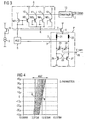
- FIG. 3 shows an embodiment of the proposed principle applied to an LC oscillator 1.
- the oscillator 1 is designed as a tunable LC resonant circuit and as such comprises two fixed value inductors 21, 22, two tunable capacitors 23, 24 and a de-attenuation amplifier 25, which comprises two cross-coupled p-channel transistors 26, 27.
- the inductors 21, 22 connect the supply current input 4 of the oscillator 1 "with the output terminal pair 3, 3 'of the oscillator 1".
- the tuning input 28 of the oscillator to which a tuning signal can be supplied, is connected via a respective varactor 23, 24 to the output terminals 3, 3 '.
- the sources of transistors 26, 27 are grounded. Depending on a gate terminal of the transistors 26, 27 is connected to a respective drain terminal of the other transistor to form a cross-coupling.
- the two drain terminals of the EntdämpfungsverEntrs 25 form the outputs 3, 3 'of the LC oscillator.
- the snubber amplifier 25 provides a negative resistance or a negative impedance.
- the time constant of the amplitude control 5, 6, 7 is interpreted much faster than the time constant of the oscillator.
- the achievable with the proposed circuit frequency deviation ranges from 10 KHz to a few megahertz.
- the possible data rate is up to several Mbit per second.
- FIG. 4 shows, on the basis of a diagram, the resonant frequency of the quartz oscillator of FIG. 2 as a function of the amplification of the amplitude control loop.
- the diagram is given in an S parameter representation.
- the loop gain is provided as a share parameter. It can be seen that varying the gain of the amplitude control loop covers a range of approximately 1800 hertz can.
- the graph thus proves the functionality of the proposed principle, namely the implementation of a frequency shift keying by switchable amplitude control of an oscillator.
- the time constant of the controller is preferably designed so that it does not respond to short-term frequency changes caused by the frequency modulation.
Claims (9)
- Ensemble oscillateur pour la modulation de fréquence, comprenant- une entrée (2) de commande pour l'entrée d'un signal (FSK) de modulation,- une sortie (3) d'oscillateur pour le prélèvement d'un signal modulé en fréquence,- un oscillateur (1) ayant une entrée (4) pour l'entrée d'un courant d'alimentation et ayant la sortie (3) d'oscillateur,- un circuit (5, 6, 7) de régulation de l'amplitude, ayant une entrée qui est reliée à la sortie (3) de l'oscillateur et ayant une sortie qui est reliée à l'entrée (4) pour l'envoi d'un courant d'alimentation de l'oscillateur (1) et- un moyen pour influencer le courant (6) d'alimentation en fonction du signal (FSK) de modulation, qui est monté dans le circuit (5, 6, 7) de régulation et qui est couplé à l'entrée (4) de l'oscillateur pour l'entrée d'un courant d'alimentation.
- Ensemble oscillateur suivant la revendication 1,
caractérisé
en ce que le moyen pour influencer le courant (6) d'alimentation comprend plusieurs interrupteurs (10, 11, 12, 13) de courant montés en parallèle. - Ensemble oscillateur suivant la revendication 2,
caractérisé
en ce que les interrupteurs (10, 11, 12, 13) de courant montés en parallèle sont disposés du côté sortie dans des trajets de courant de, respectivement, un miroir de courant (M1, M2, M3, M4, M5). - Ensemble oscillateur suivant la revendication 3,
caractérisé
en ce que le miroir de courant (M1, M2, M3, M4, M5) relie la sortie d'un bloc (5) de régulation de l'amplification relié à la sortie (3) de l'oscillateur à un noeud (K) de circuit dans un autre miroir de courant (7, 8) qui est conçu pour envoyer le courant d'alimentation de l'oscillateur (1). - Ensemble oscillateur suivant l'une des revendications 2 à 4,
caractérisé
en ce qu'il est prévu un bloc (15) de commande ayant une entrée qui forme l'entrée (2) de commande de l'ensemble oscillateur pour l'envoi d'un signal (FSK) de modulation et ayant des sorties qui sont reliées à des entrées de commande des interrupteurs (10, 11, 12, 13) de courant, conçu pour commander les interrupteurs (10, 11, 12, 13) de courant en fonction du signal (FSK) de modulation. - Ensemble oscillateur suivant l'une des revendications 1 à 5,
caractérisé
en ce que le signal (FSK) de modulation est un signal codé numériquement suivant un procédé d'échantillonnage en fréquence. - Ensemble oscillateur suivant l'une des revendications 1 à 6,
caractérisé
en ce que l'oscillateur (1) est réalisé en oscillateur accordable comprenant au moins une capacité (23) déterminant une fréquence d'oscillation et réglable en fonction d'une tension d'accord (V_tune). - Ensemble oscillateur suivant l'une des revendications 1 à 7,
caractérisé
en ce que l'oscillateur est un oscillateur LC comprenant au moins une capacité (23) déterminant une fréquence d'oscillation et au moins une inductance (21) déterminant une fréquence de circuit oscillant. - Ensemble oscillateur suivant l'une des revendications 1 à 7,
caractérisé
en ce que l'oscillateur (1) est un oscillateur à quartz ayant un quartz (16) oscillateur déterminant une fréquence d'oscillation.
Applications Claiming Priority (3)
| Application Number | Priority Date | Filing Date | Title |
|---|---|---|---|
| DE10302391 | 2003-01-22 | ||
| DE10302391A DE10302391A1 (de) | 2003-01-22 | 2003-01-22 | Oszillatoranordnung für Frequenzmodulation |
| PCT/EP2003/014461 WO2004066578A1 (fr) | 2003-01-22 | 2003-12-18 | Ensemble oscillateur utilise a des fins de modulation de frequence |
Publications (2)
| Publication Number | Publication Date |
|---|---|
| EP1586183A1 EP1586183A1 (fr) | 2005-10-19 |
| EP1586183B1 true EP1586183B1 (fr) | 2006-11-22 |
Family
ID=32694925
Family Applications (1)
| Application Number | Title | Priority Date | Filing Date |
|---|---|---|---|
| EP03782441A Expired - Fee Related EP1586183B1 (fr) | 2003-01-22 | 2003-12-18 | Ensemble oscillateur utilise a des fins de modulation de frequence |
Country Status (6)
| Country | Link |
|---|---|
| US (1) | US7369009B2 (fr) |
| EP (1) | EP1586183B1 (fr) |
| AT (1) | ATE346445T1 (fr) |
| AU (1) | AU2003290081A1 (fr) |
| DE (2) | DE10302391A1 (fr) |
| WO (1) | WO2004066578A1 (fr) |
Families Citing this family (11)
| Publication number | Priority date | Publication date | Assignee | Title |
|---|---|---|---|---|
| JP2007251228A (ja) * | 2006-03-13 | 2007-09-27 | Toshiba Corp | 電圧制御発振器、動作電流調整装置、および、電圧制御発振器の動作電流調整方法 |
| TWI323565B (en) * | 2006-06-16 | 2010-04-11 | Realtek Semiconductor Corp | Voltage-controlled oscillator |
| US7425909B2 (en) * | 2006-07-31 | 2008-09-16 | Analog Devices, Inc. | Low-noise programmable current source |
| WO2009049143A1 (fr) * | 2007-10-10 | 2009-04-16 | Georgia Tech Research Corporation | Oscillateur commandé en tension à large bande d'onde millimétrique |
| US7639097B2 (en) * | 2007-10-11 | 2009-12-29 | Freescale Semiconductor, Inc. | Crystal oscillator circuit having fast start-up and method therefor |
| US20150180412A1 (en) * | 2013-12-24 | 2015-06-25 | Realtek Semiconductor Corp. | Controllable oscillator and method thereof |
| JP6930134B2 (ja) * | 2017-02-28 | 2021-09-01 | セイコーエプソン株式会社 | 発振器、電子機器及び移動体 |
| EP3514951B1 (fr) * | 2018-01-18 | 2024-03-13 | ams AG | Agencement de circuit d'oscillateur |
| US10833633B2 (en) * | 2018-12-19 | 2020-11-10 | Semiconductor Components Industries, Llc | Circuit and method for controlling a crystal oscillator |
| TWI763116B (zh) * | 2020-11-10 | 2022-05-01 | 瑞昱半導體股份有限公司 | 振盪訊號產生電路 |
| CN114510101A (zh) * | 2020-11-16 | 2022-05-17 | 瑞昱半导体股份有限公司 | 振荡信号产生电路 |
Family Cites Families (12)
| Publication number | Priority date | Publication date | Assignee | Title |
|---|---|---|---|---|
| US2874216A (en) * | 1953-10-27 | 1959-02-17 | Gen Electric | Automatic signal control system |
| US3641460A (en) * | 1970-11-09 | 1972-02-08 | Intertel Inc | Frequency shift transmitter |
| US4071832A (en) * | 1976-06-14 | 1978-01-31 | Sperry Rand Corporation | Current controlled oscillator |
| CA1215437A (fr) * | 1983-05-25 | 1986-12-16 | Sony Corporation | Circuit oscillant a frequence variable |
| JPH0248807A (ja) | 1988-08-10 | 1990-02-19 | Hitachi Ltd | 変調回路 |
| DE3836822A1 (de) * | 1988-10-28 | 1990-05-03 | Olympia Aeg | Frequenzmodulator mit pll zur uebertragung von wahlweise nrz-datensignalen oder sprachsignalen |
| JPH0332206A (ja) | 1989-06-29 | 1991-02-12 | Nippon Denki Musen Denshi Kk | 周波数変調器 |
| US5150377A (en) | 1990-11-02 | 1992-09-22 | At&T Bell Laboratories | Direct sequence spread spectrum (dsss) communications system with frequency modulation utilized to achieve spectral spreading |
| US5323125A (en) * | 1993-03-15 | 1994-06-21 | Motorola, Inc. | Frequency agile method for transmitting multi-level data |
| US5687201A (en) * | 1995-03-21 | 1997-11-11 | Standard Microsystems Corporation | Phase-locked-loop with linear combination of charge pump and current controlled oscillator |
| US6198360B1 (en) * | 1998-10-16 | 2001-03-06 | Cypress Semiconductor Corp. | Quadrature current frequency modulation oscillator |
| US6323735B1 (en) * | 2000-05-25 | 2001-11-27 | Silicon Laboratories, Inc. | Method and apparatus for synthesizing high-frequency signals utilizing on-package oscillator circuit inductors |
-
2003
- 2003-01-22 DE DE10302391A patent/DE10302391A1/de not_active Ceased
- 2003-12-18 DE DE50305801T patent/DE50305801D1/de not_active Expired - Lifetime
- 2003-12-18 US US10/542,719 patent/US7369009B2/en not_active Expired - Fee Related
- 2003-12-18 WO PCT/EP2003/014461 patent/WO2004066578A1/fr not_active Application Discontinuation
- 2003-12-18 AT AT03782441T patent/ATE346445T1/de active
- 2003-12-18 AU AU2003290081A patent/AU2003290081A1/en not_active Abandoned
- 2003-12-18 EP EP03782441A patent/EP1586183B1/fr not_active Expired - Fee Related
Also Published As
| Publication number | Publication date |
|---|---|
| ATE346445T1 (de) | 2006-12-15 |
| AU2003290081A1 (en) | 2004-08-13 |
| EP1586183A1 (fr) | 2005-10-19 |
| US7369009B2 (en) | 2008-05-06 |
| US20060103475A1 (en) | 2006-05-18 |
| DE10302391A1 (de) | 2004-08-12 |
| DE50305801D1 (de) | 2007-01-04 |
| WO2004066578A1 (fr) | 2004-08-05 |
Similar Documents
| Publication | Publication Date | Title |
|---|---|---|
| DE60317669T2 (de) | Lc-oszillator mit grossem abstimmbereich und geringem phasenrauschen | |
| DE102006011285B4 (de) | Schwingkreisanordnung mit digitaler Steuerung, Verfahren zur Erzeugung eines Schwingungssignals und digitaler Phasenregelkreis mit der Schwingkreisanordnung | |
| DE60110686T2 (de) | Frequenzsynthesizer | |
| DE60030589T2 (de) | Verfahren zur steuerspannungsversorgung für varaktoren, zur verminderung des phasenrauschens in elektronischen oszillatoren | |
| DE69533913T2 (de) | Frequenzsynthesizer | |
| DE602005003396T2 (de) | Variable Kapazitätsschaltung mit AN/AUS Schalter für die variable Kapazitätsfunktion und selbige benutzender spannungsgesteuerter Oszillator | |
| DE102014102940A1 (de) | Oszillator mit LC-Primär- und Sekundärschwingschaltungen | |
| EP1586183B1 (fr) | Ensemble oscillateur utilise a des fins de modulation de frequence | |
| EP1195000B1 (fr) | Oscillateur commande en tension avec circuit oscillateur lc | |
| EP1069680A2 (fr) | Circuit d' accord avec au moins une première et une deuxième bande de fréquence | |
| DE102012105968A1 (de) | Oszillatorschaltung | |
| EP1223670B1 (fr) | Oscillateur commandé en tension pour modulation de fréquence | |
| DE2603641A1 (de) | Phasenstarre rueckfuehrschleife, insbesondere fuer einen breitbandsender | |
| EP0623992B1 (fr) | Oscillateur | |
| DE19949782C1 (de) | PLL-Schaltung | |
| EP1670136A1 (fr) | Oscillateur commandé en tension avec des signaux de réglage analogiques et numériques | |
| DE2946194A1 (de) | Kanalwaehleinrichtung mit frequenzsynthesator | |
| DE60009908T2 (de) | Variabler oszillator | |
| DE102004025545A1 (de) | CMOS LC-tank Oscillator | |
| DE3931513C2 (fr) | ||
| DE19837204B4 (de) | Totzeitreduzierung bei Frequenzsprüngen in Mehrfachbandsyntheseeinheiten | |
| EP1714389A2 (fr) | Circuit oscillateur destine notamment a la telephonie mobile | |
| EP1386400B1 (fr) | Boucle a phase asservie | |
| EP0893011B1 (fr) | Boucle asservie en phase avec largeur de bande commutable | |
| DE2910892A1 (de) | Schaltungsanordnung zum umwandeln analoger in digitale informationen |
Legal Events
| Date | Code | Title | Description |
|---|---|---|---|
| PUAI | Public reference made under article 153(3) epc to a published international application that has entered the european phase |
Free format text: ORIGINAL CODE: 0009012 |
|
| 17P | Request for examination filed |
Effective date: 20050708 |
|
| AK | Designated contracting states |
Kind code of ref document: A1 Designated state(s): AT BE BG CH CY CZ DE DK EE ES FI FR GB GR HU IE IT LI LU MC NL PT RO SE SI SK TR |
|
| AX | Request for extension of the european patent |
Extension state: AL LT LV MK |
|
| GRAP | Despatch of communication of intention to grant a patent |
Free format text: ORIGINAL CODE: EPIDOSNIGR1 |
|
| DAX | Request for extension of the european patent (deleted) | ||
| RBV | Designated contracting states (corrected) |
Designated state(s): AT DE FR GB IE IT |
|
| GRAS | Grant fee paid |
Free format text: ORIGINAL CODE: EPIDOSNIGR3 |
|
| GRAA | (expected) grant |
Free format text: ORIGINAL CODE: 0009210 |
|
| AK | Designated contracting states |
Kind code of ref document: B1 Designated state(s): AT DE FR GB IE IT |
|
| REG | Reference to a national code |
Ref country code: GB Ref legal event code: FG4D Free format text: NOT ENGLISH |
|
| REG | Reference to a national code |
Ref country code: IE Ref legal event code: FG4D Free format text: LANGUAGE OF EP DOCUMENT: GERMAN |
|
| REF | Corresponds to: |
Ref document number: 50305801 Country of ref document: DE Date of ref document: 20070104 Kind code of ref document: P |
|
| GBT | Gb: translation of ep patent filed (gb section 77(6)(a)/1977) |
Effective date: 20070228 |
|
| ET | Fr: translation filed | ||
| PLBE | No opposition filed within time limit |
Free format text: ORIGINAL CODE: 0009261 |
|
| STAA | Information on the status of an ep patent application or granted ep patent |
Free format text: STATUS: NO OPPOSITION FILED WITHIN TIME LIMIT |
|
| 26N | No opposition filed |
Effective date: 20070823 |
|
| PGFP | Annual fee paid to national office [announced via postgrant information from national office to epo] |
Ref country code: IE Payment date: 20121226 Year of fee payment: 10 |
|
| PGFP | Annual fee paid to national office [announced via postgrant information from national office to epo] |
Ref country code: IT Payment date: 20121219 Year of fee payment: 10 Ref country code: GB Payment date: 20121227 Year of fee payment: 10 |
|
| PGFP | Annual fee paid to national office [announced via postgrant information from national office to epo] |
Ref country code: AT Payment date: 20121204 Year of fee payment: 10 Ref country code: FR Payment date: 20130110 Year of fee payment: 10 |
|
| REG | Reference to a national code |
Ref country code: AT Ref legal event code: MM01 Ref document number: 346445 Country of ref document: AT Kind code of ref document: T Effective date: 20131218 |
|
| GBPC | Gb: european patent ceased through non-payment of renewal fee |
Effective date: 20131218 |
|
| REG | Reference to a national code |
Ref country code: IE Ref legal event code: MM4A |
|
| REG | Reference to a national code |
Ref country code: FR Ref legal event code: ST Effective date: 20140829 |
|
| PG25 | Lapsed in a contracting state [announced via postgrant information from national office to epo] |
Ref country code: IE Free format text: LAPSE BECAUSE OF NON-PAYMENT OF DUE FEES Effective date: 20131218 |
|
| PG25 | Lapsed in a contracting state [announced via postgrant information from national office to epo] |
Ref country code: FR Free format text: LAPSE BECAUSE OF NON-PAYMENT OF DUE FEES Effective date: 20131231 Ref country code: GB Free format text: LAPSE BECAUSE OF NON-PAYMENT OF DUE FEES Effective date: 20131218 Ref country code: AT Free format text: LAPSE BECAUSE OF NON-PAYMENT OF DUE FEES Effective date: 20131218 |
|
| PG25 | Lapsed in a contracting state [announced via postgrant information from national office to epo] |
Ref country code: IT Free format text: LAPSE BECAUSE OF NON-PAYMENT OF DUE FEES Effective date: 20131231 |
|
| PG25 | Lapsed in a contracting state [announced via postgrant information from national office to epo] |
Ref country code: IT Free format text: LAPSE BECAUSE OF NON-PAYMENT OF DUE FEES Effective date: 20131218 |
|
| PGFP | Annual fee paid to national office [announced via postgrant information from national office to epo] |
Ref country code: DE Payment date: 20181214 Year of fee payment: 16 |
|
| REG | Reference to a national code |
Ref country code: DE Ref legal event code: R119 Ref document number: 50305801 Country of ref document: DE |
|
| PG25 | Lapsed in a contracting state [announced via postgrant information from national office to epo] |
Ref country code: DE Free format text: LAPSE BECAUSE OF NON-PAYMENT OF DUE FEES Effective date: 20200701 |