EP1580866A1 - Kaskadierbares Halbleiterbauelement zur Ladungsüberwachung der Kondensatoren - Google Patents
Kaskadierbares Halbleiterbauelement zur Ladungsüberwachung der Kondensatoren Download PDFInfo
- Publication number
- EP1580866A1 EP1580866A1 EP05251826A EP05251826A EP1580866A1 EP 1580866 A1 EP1580866 A1 EP 1580866A1 EP 05251826 A EP05251826 A EP 05251826A EP 05251826 A EP05251826 A EP 05251826A EP 1580866 A1 EP1580866 A1 EP 1580866A1
- Authority
- EP
- European Patent Office
- Prior art keywords
- voltage side
- power supply
- semiconductor apparatus
- connection
- transistor
- Prior art date
- Legal status (The legal status is an assumption and is not a legal conclusion. Google has not performed a legal analysis and makes no representation as to the accuracy of the status listed.)
- Granted
Links
Images


Classifications
-
- H—ELECTRICITY
- H02—GENERATION; CONVERSION OR DISTRIBUTION OF ELECTRIC POWER
- H02J—ELECTRIC POWER NETWORKS; CIRCUIT ARRANGEMENTS OR SYSTEMS FOR SUPPLYING OR DISTRIBUTING ELECTRIC POWER; SYSTEMS FOR STORING ELECTRIC ENERGY
- H02J7/00—Circuit arrangements for charging or discharging batteries or for supplying loads from batteries
- H02J7/50—Circuit arrangements for charging or discharging batteries or for supplying loads from batteries acting upon multiple batteries simultaneously or sequentially
- H02J7/52—Circuit arrangements for charging or discharging batteries or for supplying loads from batteries acting upon multiple batteries simultaneously or sequentially for charge balancing, e.g. equalisation of charge between batteries
- H02J7/54—Passive balancing, e.g. using resistors or parallel MOSFETs
-
- H—ELECTRICITY
- H02—GENERATION; CONVERSION OR DISTRIBUTION OF ELECTRIC POWER
- H02J—ELECTRIC POWER NETWORKS; CIRCUIT ARRANGEMENTS OR SYSTEMS FOR SUPPLYING OR DISTRIBUTING ELECTRIC POWER; SYSTEMS FOR STORING ELECTRIC ENERGY
- H02J7/00—Circuit arrangements for charging or discharging batteries or for supplying loads from batteries
- H02J7/34—Parallel operation in networks using both storage and other DC sources, e.g. providing buffering
- H02J7/345—Parallel operation in networks using both storage and other DC sources, e.g. providing buffering using capacitors as storage or buffering devices
Definitions
- the present invention generally relates to a semiconductor apparatus for charging a capacitor, and more particularly, to a semiconductor apparatus in which multiple parallel monitor circuits are integrated for evenly charging multiple electric double layer capacitors connected in series.
- An electric double layer capacitor can be charged more quickly than a secondary battery is. Additionally, an electric double layer capacitor can store more energy than a secondary battery can. Since the rated voltage of an electric double layer capacitor is about 2.7 V, if a higher voltage is required, multiple capacitors connected in series are used.
- a circuit called "parallel monitor" for evenly charging multiple capacitors is used to solve the above problem.
- FIG. 4 is a circuit diagram showing a portion of a parallel monitor circuit disclosed in Japanese Patent Laid-Open Application No. 2000-050495.
- the same parallel monitor as shown in FIG. 4 is provided to each one of multiple capacitors connected in series.
- the parallel monitor is described below with reference to FIG. 4.
- the parallel monitor circuit shown in FIG. 4 includes reference voltages Vr1 and Vr2, a comparator circuit CMP for comparing the voltage of a capacitor C1 with the reference voltage Vr1 or Vr2, switches S1 and S2 for switching the reference voltages Vr1 and Vr2, a transistor Tr1 for bypassing the charge current that flows into the capacitor C1, and a switch control circuit for controlling the switches S1 and S2 in accordance with the output of the comparator circuit CMP.
- the reference voltage Vr1 is set at 3 V which is the full charge voltage of the capacitor C1, and the reference voltage Vr2 is set at 0.8 V which is less than the full charge voltage of the capacitor C1.
- the switch S1 is connected to the reference voltage Vr2.
- the output of the comparator circuit CMP is inverted, and turns on the transistor Tr1.
- the transistor Tr1 is turned on, the capacitor C1 is discharged, and the time constant of the discharge is determined by the resistance component of the circuit including the transistor Tr1.
- the switch control circuit monitors the outputs of all comparator circuits CMP. While the capacitor C1 is discharged, if the charge voltage of another capacitor increases up to the reference voltage 0.8 V, the switch S1 is switched to the reference voltage Vr1, and bypass mode is discharged. The capacitors are charged up to the full charge voltage 3 V.
- the quantity of the parallel monitor circuits required is equal to the number of capacitors that are connected in series.
- the scale of the entire parallel monitor circuits become large.
- the conventional parallel monitor circuits have not integrated in a semiconductor apparatus but assembled using discrete components.
- the scale of the conventional parallel monitor circuits are large, and their cost is high.
- the integration of the parallel monitor circuits are desired to solve the above problem.
- the quantity of capacitors connected in series depends on their application. It is not practical to design and manufacture a semiconductor apparatus in which the suitable number of parallel monitor circuits are integrated for each application.
- the semiconductor apparatus IC1 five through ten parallel monitor circuits are integrated in a semiconductor apparatus IC1 (five in the case of FIG. 1) as shown in FIG. 1. If there are capacitors more than the parallel monitor circuits integrated in one semiconductor apparatus that are to be charged, the semiconductor apparatuses are cascaded as many as necessary. According to the above arrangements, the reasonable number of parallel monitor circuits can be integrated in a semiconductor apparatus so as to increase the efficiency of integration and consequently to reduce the cost of the parallel monitor circuits.
- the control circuit for monitoring the output of the comparator circuit CMP and for switching the reference voltages is configured by a CPU, for example, and the control circuit is usually separate from the semiconductor apparatus as shown in FIG. 4.
- the voltage applied to the power supply voltages Vdd (plus) and Vss (minus) of each monitor IC may be different.
- the voltage level of signal lines for exchanging signals with the control circuit may differ for each monitor IC. It is impossible to directly connect the control circuit and all monitor ICs.
- This problem can be solved by a technique in which wiring is made between the control circuit and the monitor IC1, the minus power supply voltage Vss of which is common to the minus power supply voltage Vss of the control circuit, and the monitor IC1 shifts the voltage level of the control signal, and the control signal line is connected from the terminal of the monitor IC1 to the terminal of the monitor IC2 as shown in FIG. 1.
- This connection technique is referred to as daisy chain.
- the plus power supply voltage Vdd of the monitor IC1 is the minus power supply voltage Vss of the monitor IC2
- voltage between the minus power supply voltage Vss of the monitor IC1 and the plus power supply voltage Vdd of the monitor IC2 is applied to terminals CON1 through CON12 that connects the monitor IC1 and the monitor IC2.
- the monitor IC1 and monitor IC2 need to have withstanding voltage twice as high as the power supply voltage of the monitor IC in the case in which one monitor IC charges one capacitor. Since a high withstanding voltage transistor is larger than a low withstanding voltage transistor, the chip size and cost of the monitor IC is increased.
- Another and more specific object of the present invention is to provide a semiconductor apparatus for charging a capacitor that can be used without increasing its withstanding voltage.
- a semiconductor apparatus includes:
- FIG. 1 is a circuit diagram showing the case in which two monitor ICs according to an embodiment are cascaded. The signal flow between a control circuit and the monitor ICs is described below with reference to FIG. 1.
- Terminals CON1-12 at the left side of each monitor IC IC1-2 are control terminals for controlling charge.
- the terminal to which a black dot is indicated is an output terminal, and the terminal to which an arrow is indicated is an input terminal.
- Neither a black dot nor an arrow is indicated to the terminals at the right side of each monitor IC which are used for controlling the bypass of a capacitor.
- the arrows indicated on connections between the control circuit and the monitor IC1 and between the monitor IC1 and the monitor IC2 indicate the directions in which signals low.
- the first type is signal flow from the control circuit to the monitor IC1, and from the monitor IC1 to the monitor IC2. This type of signal flow is referred to as "upstream" signal.
- the terminals CON9-12 and CON1-4 correspond to this type of signal flow.
- the second type is signal flow from the monitor IC2 which is at high voltage side to the monitor IC1 which is at low voltage side, and from the monitor IC1 to the control circuit. This type of signal flow is referred to as "downstream" signal.
- the terminals CON5-8 corresponds to this type of signal flow.
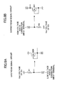
- FIGs. 2A and 2B are circuit diagrams each showing a circuit structure around the control terminal.
- FIG. 2A shows a circuit for upstream signal used for the upstream signal terminal according to an embodiment.
- This circuit includes a low voltage side IC connection input terminal and a high voltage side IC connection output terminal.
- the low voltage side IC connection input terminal is pulled up to the plus power supply voltage Vdd of the monitor IC by a pull-up resistance R1.
- the low voltage side IC connection input terminal is connected to the gate of a PMOS transistor M1.
- the source of the PMOS transistor M1 is connected to the plus power supply voltage Vdd, and the drain thereof is connected to the minus power supply voltage Vss via a resistance R2.
- the node between the drain of the PMOS transistor M1 and the resistance R2 is connected to the inside of the monitor IC as a control signal, and connected to the gate of a NMOS transistor M2.
- the source of the NMOS transistor M2 is connected to the minus power supply voltage Vss, and the drain thereof is connected to the high voltage side IC connection output terminal.
- terminals CON9-12 shown in FIG. 1 are the low voltage side IC connection input terminals
- terminals CON4-1 shown in FIG. 1 are the high voltage side IC connection output terminals corresponding to the respective low voltage side IC connection input terminals.
- FIG. 2B shows a downstream signal circuit used for the downstream signal terminal according to an embodiment.
- This circuit includes a high voltage side IC connection input terminal and a low voltage side IC connection output terminal.
- the high voltage side IC connection input terminal is pulled down to the minus power supply Vss of the monitor IC via a pull-down resistance R3.
- the high voltage side IC connection input terminal is connected to the gate of the NMOS transistor M3.
- the source of the NMOS transistor M3 is connected to the minus power supply voltage Vss, and the drain thereof is connected to the plus power supply Vdd via a resistance R4.
- the source and drain of the NMOS transistor M4 are connected to the source and drain of the NMOS transistor M3, respectively.
- a signal output from the inside of the monitor IC is fed to the gate of a NMOS transistor M4 as an alarm signal.
- the node between the drain of the NMOS transistor M3 and the resistance R4 is connected to the gate of a PMOS transistor M5.
- the source of the PMOS transistor M5 is connected to the plus power supply voltage Vdd, and the drain thereof is connected to the low voltage side IC connection output terminal.
- the terminals CON5 and 6 correspond to the high voltage side IC connection input terminal
- the terminals CON8 and 7 correspond to the low voltage side IC connection output terminal.
- FIGs. 3A and 3B are circuit diagrams showing the connection of control terminals according to an embodiment.
- FIG. 3A shows a circuit in which the upstream signal terminals of the monitor IC1 and the monitor IC2 are connected in daisy chain.
- the circuit is divided into two portions by a broken line, in which the portion above the broken line is the upstream signal circuit of the monitor IC2 and the portion below the broken line is the upstream signal circuit of the monitor IC1.
- FIG. 3A shows the terminals CON1 and CON12, the terminals CON2 and CON11, CON3 and CON10, CON4 and CON9 can be connected in the same manner.
- the monitor IC 2 Since the high voltage side IC connection output terminal CON 1 of the monitor IC 1 and the low voltage side IC connection input terminal CON 12 of the monitor IC 2 are connected, the low voltage side IC connection input terminal CON 12 of the monitor IC 2 is turned to low level. As a result, the monitor IC 2 operates in the exactly same manner as the monitor IC 1 as described above. The high voltage side IC connection output terminal CON 1 of the monitor IC 2 also outputs low level.
- the drain of the NMOS transistor M12 of the monitor IC 1 is connected to the plus power supply Vdd of the monitor IC 2 via a resistance R21 of the monitor IC 2. While the NMOS transistor M12 is turned off, the drain of the NMOS transistor M12 is provided with the plus power supply Vdd of the monitor IC 2.
- the gate of the PMOS transistor M21 of the monitor IC 2 is connected to the drain of the NMOS transistor M12 of the monitor IC 1 via the connection terminal. Because the minus power supply voltage Vss of the monitor IC 1 is applied to the gate of the PMOS transistor M21 while the NMOS transistor M12 is on, voltage twice as high as the power supply voltage (Vdd-Vss) of the monitor IC 2 is also applied to the gate of the PMOS transistor M21.
- the gate voltage of the NMOS transistors M12 and M22 that is sent to the inside of the monitor IC as a control signal is within the range of the power supply voltage of each monitor IC.
- the internal circuit of the monitor IC does not need to be made with transistors of high withstanding voltage.
- transistors M11, M12, M21, and M22 that are directly connected to terminals for input/output the control signal need to be of high withstanding voltage.
- the voltage twice as high as the power supply voltage of the monitor IC n is applied to the gate of the transistors M11 and M22, but only the voltage within the range of the power supply of the monitor IC n is applied between the source and drain thereof. It suffices that the gate dielectric film is of high withstanding voltage.
- FIG. 3B shows a circuit in which the downstream terminals of the monitor IC 1 and the monitor IC 2 are connected in daisy chain.
- the circuit is divided into two portion by a broken line.
- the upper portion above the broken line is the downstream signal circuit of the monitor IC 2
- the lower portion below the broken line is the downstream signal circuit of the monitor IC 1.
- a circuit including CON 5 and CON 8 is shown in FIG. 3B, a circuit including CON 6 and CON 7 is the same.
- the NMOS transistor M23 When a high level signal is input to the high voltage side IC connection input terminal CON 8 of the monitor IC 2, the NMOS transistor M23 is turned on. The gate voltage of the PMOS transistor M25 is lowered, and the PMOS transistor M25 is also turned on. As a result, the low voltage side IC connection output terminal CON 8 outputs a high level signal.
- the NMOS transistor M24 is turned on. Because the gate voltage of the PMOS transistor M25 is lowered, the PMOS transistor M25 is also turned on. As a result, the low voltage side IC connection output terminal CON 8 outputs a high level signal.
- a high level signal can be output to the low voltage side IC connection output terminal as the alarm signal output from the internal circuit of a monitor IC in the middle of the cascade.
- the monitor IC 1 Since the low voltage side IC connection output terminal CON 8 of the monitor IC 2 is connected to the high voltage side IC connection input terminal CON 5 of the monitor IC 1, the high voltage level IC connection input terminal CON 5 of the monitor IC 1 becomes high level. Consequently, the monitor IC 1 operates in the exactly same manner as the monitor IC 2 does, and the low voltage side IC connection output terminal CON 8 of the monitor IC 1 also outputs a high level signal.
- the drain of the PMOS transistor of the monitor IC 2 is connected to the minus power supply Vss of the monitor IC 1. Therefore, because the minus power supply voltage Vss of the monitor IC 1 is applied to the drain of the PMOS transistor M25 while the PMOS transistor M25 is turned off, the voltage twice as high as the power supply voltage of the monitor IC 2 is applied between the source and drain of the PMOS transistor M25.
- the gate of the NMOS transistor M13 of the monitor IC 1 is connected to the drain of the PMOS transistor M25 of the monitor IC 2. Consequently, while the PMOS transistor M25 is turned on, the plus power supply voltage Vdd of the monitor IC 2 is applied to the gate of the NMOS transistor M13. It is understood that the voltage twice as high as the power supply voltage of the monitor IC 1 is applied to the gate of the NMOS transistor M13.
- the internal circuit of the monitor IC can be designed without using transistors of high withstanding voltage.
- transistors M23, M25, M13, and M15 that are directly connected to the terminals for input and output the control signal need to be made of high withstanding voltage.
- the voltage twice as high as the power supply voltage of the monitor IC n is applied to the gate, but only the voltage within the range of power supply voltage is applied between the source and drain. Therefore, it suffices that the gate dielectric film is designed to be of high withstanding voltage.
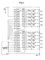
- FIG. 5 is a circuit diagram showing a circuit in which three semiconductor apparatuses according to an embodiment are cascaded.
- terminals CON 1 and CON 12, CON 2 and CON 11, CON 3 and CON 10, CON 4 and CON 9 are connected in daisy chain in the upstream signal circuit from the monitor IC 1 to the monitor IC 3.
- terminals con7 and CON 6, and CON 8 and CON 5 are connected in daisy chain.
- terminals CON 9 - CON 12 are the low voltage side IC connection input terminals of the upstream signal circuit
- terminals CON 4 - CON 1 are the corresponding high voltage side IC connection output terminals.
- the terminals CON 5 and CON 6 are the high voltage side IC connection input terminal of the download signal circuit, and the terminals CON 8 and CON 7 are the corresponding low voltage side IC connection output terminals.
- FIG. 6 is a circuit diagram showing the case in which n semiconductor apparatuses according to an embodiment are cascaded.
- terminals CON 1 and CON 12, CON 2 and CON 11, CON 3 and CON 10, CON 4 and CON 9 are connected in daisy chain in the upstream circuit as the case of two or three semiconductor apparatuses being cascaded.
- terminals CON 7 and CON 6, CON 8 and CON 5 are connected in daisy chain.
- FIGs. 7A and 7B are circuit diagram in the case in which the resistances of FIG. 2 are replaced with transistors.
- the resistance R1 is replaced with a NMOS transistor M34, and the resistance R2 is replaced with a NMOS transistor M33.
- transistors M31, M32, M33, and M34 in the upstream signal circuit are made high withstanding voltage transistors.
- voltage twice as high as the power supply voltage of the monitor IC n is applied only to the gate, but only voltage within the range of the power supply voltage of the monitor IC n is applied between the source and drain. Accordingly, it suffices that only the gate dielectric film needs to be specified as being high withstanding voltage.
- the resistance R3 is replaced with a NMOS transistor M41
- the resistance R4 is replaced with a NMOS transistor M46.
- Transistors M41, M42, M43, and M45 need to be of high withstanding voltage.
- voltage twice as high as the power supply voltage of the monitor IC n is applied to the gate, but voltage that is applied between the source and drain is the power supply voltage of the monitor IC n.
- only the gate dielectric film of the gate needs to be of high withstanding voltage.
- FIGs. 8A and 8B are circuit diagrams for explaining the input pull-down/pull-up portions configured with the resistances of FIG. 2 and the transistors of FIG. 7.
- the resistances R1 and R3 in FIG. 2 need to be high so as to reduce current that flows through the resistances. For example, if 5 V is applied to the resistance but the current needs to be reduced to 1 ⁇ A, the resistance needs to be 5 M ⁇ .
- the chip area required in the case the resistance is constructed by N channel depletion transistor M34 or M41 as shown in FIG. 8 is less than the chip area required in the case the resistance is constructed by usual resistor. Even in the case in which higher voltage is applied, the resistance constructed by the N channel depletion transistor little depends on the power supply voltage.
- the high voltage side IC connection output terminal is a N channel open drain.
- the high voltage side IC connection input terminal is the opposite terminal of a high resistance component connected to Vss, and is an inverter input terminal.
- the low voltage side IC connection output terminal is P channel open drain.
- the low voltage side IC connection input terminal is the opposite terminal of a high resistance component connected to Vdd, and an inverter input terminal.
- the high voltage side IC connection output terminal of the IC n becomes Vss voltage level of the IC n.
- the corresponding low voltage side IC connection input terminal of IC n+1 receives the low signal of IC n, a little current flows through the high resistance component connected to Vdd of IC n+1, but the low signal is fed to the inverter input.
- the signal is further transferred to the internal circuit of IC n+1, and the N channel open drain of the high voltage side IC connection output terminal of IC n+1 is turned on.
- the signal is further transferred to IC n+2.
- the high voltage side IC connection output terminal of IC n becomes Vdd voltage of IC n+1 since the high voltage side IC connection output terminal of IC n is pulled by the high resistance component connected to the corresponding low voltage side IC connection input terminal of IC n+1, the high resistance component connected to Vdd.
- a high signal is fed to the inverter input of the low voltage side IC connection input terminal of IC n+1.
- the signal is transferred through the internal circuit of IC n+1, and the N channel open drain of the high voltage side IC connection output terminal of IC n+1 is turned off. The signal is further transferred to IC n+2.
- the low voltage side IC connection output terminal of IC n becomes Vss voltage of IC n-1 since the low voltage side IC connection output terminal of IC n-1 is pulled by the high resistance component connected to the corresponding high voltage side IC connection input terminal of IC n-1, the high resistance component connected to Vss.
- a low signal is fed to the inverter input of the high voltage side IC connection input terminal of IC n-1.
- the signal is transferred through the internal circuit of IC n-1, and the P channel open drain of the low voltage side IC connection output terminal of IC n-1 is turned off. The signal is further transferred to IC n-2.
- the construction of the control terminal is not limited to the technique and system described above. Those skilled in the art will recognize various modifications to the present invention without departing from the scope of the appended claims.
- the present invention is applicable to a semiconductor apparatus having any suitable type of terminals such as pin insertion type and surface mount type.
- An example of the surface mount type may include ball grid type, gull-wing lead type, and J lead type.
- the present invention also is applicable to a semiconductor apparatus embedded in any suitable package having opposing edges at which leads are disposed.
- An example of the package may include DIP, PGA, SOP, QFP, BGA, and CSP.
Landscapes
- Engineering & Computer Science (AREA)
- Power Engineering (AREA)
- Semiconductor Integrated Circuits (AREA)
- Charge And Discharge Circuits For Batteries Or The Like (AREA)
Applications Claiming Priority (2)
| Application Number | Priority Date | Filing Date | Title |
|---|---|---|---|
| JP2004084620A JP4019376B2 (ja) | 2004-03-23 | 2004-03-23 | キャパシタ充電用半導体装置 |
| JP2004084620 | 2004-03-23 |
Publications (2)
| Publication Number | Publication Date |
|---|---|
| EP1580866A1 true EP1580866A1 (de) | 2005-09-28 |
| EP1580866B1 EP1580866B1 (de) | 2009-10-28 |
Family
ID=34858398
Family Applications (1)
| Application Number | Title | Priority Date | Filing Date |
|---|---|---|---|
| EP05251826A Expired - Lifetime EP1580866B1 (de) | 2004-03-23 | 2005-03-23 | Kaskadierbares Halbleiterbauelement zur Ladungsüberwachung der Kondensatoren |
Country Status (5)
| Country | Link |
|---|---|
| US (1) | US7495418B2 (de) |
| EP (1) | EP1580866B1 (de) |
| JP (1) | JP4019376B2 (de) |
| DE (1) | DE602005017324D1 (de) |
| ES (1) | ES2334922T3 (de) |
Cited By (1)
| Publication number | Priority date | Publication date | Assignee | Title |
|---|---|---|---|---|
| EP1933443A3 (de) * | 2006-12-13 | 2016-02-24 | Semiconductor Components Industries, LLC | Leistungszellenüberwachung |
Families Citing this family (13)
| Publication number | Priority date | Publication date | Assignee | Title |
|---|---|---|---|---|
| CN102437384B (zh) | 2006-11-06 | 2014-08-06 | 日本电气株式会社 | 电池控制系统以及电池控制方法 |
| JP2009004979A (ja) * | 2007-06-20 | 2009-01-08 | Nec Electronics Corp | インダクタンス負荷駆動装置、及び、フライバック電圧検出回路 |
| CN101399440B (zh) * | 2007-09-27 | 2011-03-30 | 比亚迪股份有限公司 | 一种多节电池的保护电路及方法 |
| US8525487B1 (en) * | 2008-03-05 | 2013-09-03 | Marvell International Ltd. | Circuit and method for regulating discharge of a capacitor |
| CN101488671B (zh) * | 2009-02-24 | 2011-01-12 | 浙江大学 | 一种多节串联锂离子电池包的管理模块 |
| US8089248B2 (en) * | 2009-04-09 | 2012-01-03 | Ford Global Technologies, Llc | Battery monitoring and control system and method of use including redundant secondary communication interface |
| CA2716022C (en) | 2010-09-30 | 2019-03-12 | Light-Based Technologies Incorporated | Apparatus and methods for supplying power |
| JP5438542B2 (ja) * | 2010-02-15 | 2014-03-12 | 矢崎総業株式会社 | 電圧検出装置 |
| EP2656496B1 (de) | 2010-12-22 | 2019-09-11 | GE Energy Power Conversion Technology Limited | Mechanische anordnung einer mehrstufigen stromrichterschaltungsanordnung |
| US9312705B2 (en) | 2010-12-22 | 2016-04-12 | Ge Energy Power Conversion Technology Limited | Capacitor balancing circuit and control method for an electronic device such as a multilevel power inverter |
| CN104518767B (zh) * | 2014-07-18 | 2017-10-24 | 上海华虹宏力半导体制造有限公司 | 时钟幅度加倍电路 |
| KR20170125916A (ko) * | 2015-03-05 | 2017-11-15 | 리니어 테크놀러지 엘엘씨 | 저전압 임계의 정확한 검출 |
| CN111130151B (zh) * | 2019-11-28 | 2021-02-19 | 中国地质大学(武汉) | 可自关断自启动的低功耗电压监视电路 |
Citations (5)
| Publication number | Priority date | Publication date | Assignee | Title |
|---|---|---|---|---|
| US4948954A (en) * | 1989-05-15 | 1990-08-14 | Dallas Semiconductor Corporation | Interface for receiving electronic tokens |
| US5537076A (en) * | 1993-05-25 | 1996-07-16 | Nec Corporation | Negative resistance circuit and inverter circuit including the same |
| US5998969A (en) * | 1997-05-12 | 1999-12-07 | Nissan Motor Co., Ltd. | Apparatus for regulating state of charge of cells of battery set |
| US6133710A (en) * | 1998-08-27 | 2000-10-17 | Jeol Ltd. | Electrical storage capacitor system |
| US6240101B1 (en) * | 1998-05-20 | 2001-05-29 | Kingston Technology Co. | Bi-directional daisy-chain cascading of network repeaters |
Family Cites Families (15)
| Publication number | Priority date | Publication date | Assignee | Title |
|---|---|---|---|---|
| JPH06343225A (ja) * | 1993-05-28 | 1994-12-13 | Asahi Glass Co Ltd | 蓄電電源装置 |
| JP3069498B2 (ja) * | 1994-09-01 | 2000-07-24 | 富士通株式会社 | 充放電装置および電子機器 |
| US5631537A (en) * | 1995-10-17 | 1997-05-20 | Benchmarq Microelectronics | Battery charge management/protection apparatus |
| FR2743953B1 (fr) * | 1996-01-19 | 1998-04-10 | Sgs Thomson Microelectronics | Circuit d'alimentation a condensateur de stockage |
| US5982050A (en) * | 1996-03-14 | 1999-11-09 | Fuji Jukogyo Kabushiki Kaisha | Power supply unit for automotive vehicle |
| US5734205A (en) * | 1996-04-04 | 1998-03-31 | Jeol Ltd. | Power supply using batteries undergoing great voltage variations |
| JP3313647B2 (ja) | 1998-07-27 | 2002-08-12 | 株式会社岡村研究所 | キャパシタ充電監視制御装置 |
| US6225781B1 (en) * | 1998-08-27 | 2001-05-01 | Jeol Ltd. | System for charging capacitors connected in series |
| EP1020973A3 (de) * | 1999-01-18 | 2001-05-02 | Hitachi, Ltd. | Ladungs- und Entladungssystem für eine elektrische Energiespeicheranlage |
| US6316917B1 (en) * | 1999-03-09 | 2001-11-13 | Asahi Glass Company, Limited | Apparatus having plural electric double layer capacitors and method for adjusting voltages of the capacitors |
| US6323623B1 (en) * | 1999-08-23 | 2001-11-27 | Casio Computer Co., Ltd. | Charging device and charging method thereof |
| JP3855565B2 (ja) * | 1999-11-02 | 2006-12-13 | 株式会社リコー | 充放電保護回路および該充放電保護回路を有するバッテリーパック |
| JP3364836B2 (ja) * | 2000-10-19 | 2003-01-08 | 富士重工業株式会社 | 電圧イコライザ装置およびその方法 |
| JP2004080087A (ja) * | 2002-08-09 | 2004-03-11 | Renesas Technology Corp | 過電流検出回路 |
| JP2004336919A (ja) * | 2003-05-09 | 2004-11-25 | Ricoh Co Ltd | キャパシタ充電回路およびそれに用いる半導体装置 |
-
2004
- 2004-03-23 JP JP2004084620A patent/JP4019376B2/ja not_active Expired - Lifetime
-
2005
- 2005-03-22 US US11/085,107 patent/US7495418B2/en not_active Expired - Lifetime
- 2005-03-23 ES ES05251826T patent/ES2334922T3/es not_active Expired - Lifetime
- 2005-03-23 DE DE602005017324T patent/DE602005017324D1/de not_active Expired - Lifetime
- 2005-03-23 EP EP05251826A patent/EP1580866B1/de not_active Expired - Lifetime
Patent Citations (5)
| Publication number | Priority date | Publication date | Assignee | Title |
|---|---|---|---|---|
| US4948954A (en) * | 1989-05-15 | 1990-08-14 | Dallas Semiconductor Corporation | Interface for receiving electronic tokens |
| US5537076A (en) * | 1993-05-25 | 1996-07-16 | Nec Corporation | Negative resistance circuit and inverter circuit including the same |
| US5998969A (en) * | 1997-05-12 | 1999-12-07 | Nissan Motor Co., Ltd. | Apparatus for regulating state of charge of cells of battery set |
| US6240101B1 (en) * | 1998-05-20 | 2001-05-29 | Kingston Technology Co. | Bi-directional daisy-chain cascading of network repeaters |
| US6133710A (en) * | 1998-08-27 | 2000-10-17 | Jeol Ltd. | Electrical storage capacitor system |
Cited By (1)
| Publication number | Priority date | Publication date | Assignee | Title |
|---|---|---|---|---|
| EP1933443A3 (de) * | 2006-12-13 | 2016-02-24 | Semiconductor Components Industries, LLC | Leistungszellenüberwachung |
Also Published As
| Publication number | Publication date |
|---|---|
| US7495418B2 (en) | 2009-02-24 |
| JP2005278243A (ja) | 2005-10-06 |
| EP1580866B1 (de) | 2009-10-28 |
| JP4019376B2 (ja) | 2007-12-12 |
| DE602005017324D1 (de) | 2009-12-10 |
| US20050231173A1 (en) | 2005-10-20 |
| ES2334922T3 (es) | 2010-03-17 |
Similar Documents
| Publication | Publication Date | Title |
|---|---|---|
| US8058845B2 (en) | Battery state monitoring circuit and battery apparatus | |
| EP1580866A1 (de) | Kaskadierbares Halbleiterbauelement zur Ladungsüberwachung der Kondensatoren | |
| US8319476B2 (en) | Battery state monitoring circuit and battery device | |
| EP2193588B1 (de) | Mehrzellenschutzschaltung und verfahren | |
| US7397221B2 (en) | Battery protection device, battery protection system using the same, and battery protection method | |
| US6259306B1 (en) | Control system for a bidirectional switch with two transistors | |
| JP3592674B2 (ja) | 充放電制御回路と充電式電源装置 | |
| JP2001352683A (ja) | 充放電式電源装置 | |
| CN101160687B (zh) | 用于电池单元平衡的开关电路 | |
| CN114252775A (zh) | 电流检测芯片、电池及电子设备 | |
| JP3597618B2 (ja) | 二次電池保護回路 | |
| US11159028B2 (en) | Battery control circuit, battery control device, and battery pack | |
| CN112865253B (zh) | 驱动电路、集成器件、电池管理芯片及电池管理系统 | |
| JP3944855B2 (ja) | キャパシタ充電用半導体装置 | |
| JP4169128B2 (ja) | キャパシタ充電用半導体装置 | |
| JP2007218680A (ja) | 充放電監視装置 | |
| CN213521313U (zh) | 单晶圆电池保护电路、电池充放电电路及便携式电子设备 | |
| CN222762247U (zh) | 锂电池的测量电路以及锂电池系统 | |
| US8867246B2 (en) | Communication device and battery pack in which the communication device is provided | |
| CN119561216A (zh) | 供电电路、方法、芯片及电子设备 | |
| JPH08293770A (ja) | 半導体遅延回路 | |
| JPH0774614A (ja) | 半導体集積回路 |
Legal Events
| Date | Code | Title | Description |
|---|---|---|---|
| PUAI | Public reference made under article 153(3) epc to a published international application that has entered the european phase |
Free format text: ORIGINAL CODE: 0009012 |
|
| 17P | Request for examination filed |
Effective date: 20050412 |
|
| AK | Designated contracting states |
Kind code of ref document: A1 Designated state(s): AT BE BG CH CY CZ DE DK EE ES FI FR GB GR HU IE IS IT LI LT LU MC NL PL PT RO SE SI SK TR |
|
| AX | Request for extension of the european patent |
Extension state: AL BA HR LV MK YU |
|
| AKX | Designation fees paid |
Designated state(s): DE ES FR GB IT NL |
|
| 17Q | First examination report despatched |
Effective date: 20060629 |
|
| GRAP | Despatch of communication of intention to grant a patent |
Free format text: ORIGINAL CODE: EPIDOSNIGR1 |
|
| GRAS | Grant fee paid |
Free format text: ORIGINAL CODE: EPIDOSNIGR3 |
|
| GRAA | (expected) grant |
Free format text: ORIGINAL CODE: 0009210 |
|
| AK | Designated contracting states |
Kind code of ref document: B1 Designated state(s): DE ES FR GB IT NL |
|
| REG | Reference to a national code |
Ref country code: GB Ref legal event code: FG4D |
|
| REF | Corresponds to: |
Ref document number: 602005017324 Country of ref document: DE Date of ref document: 20091210 Kind code of ref document: P |
|
| REG | Reference to a national code |
Ref country code: ES Ref legal event code: FG2A Ref document number: 2334922 Country of ref document: ES Kind code of ref document: T3 |
|
| PLBE | No opposition filed within time limit |
Free format text: ORIGINAL CODE: 0009261 |
|
| STAA | Information on the status of an ep patent application or granted ep patent |
Free format text: STATUS: NO OPPOSITION FILED WITHIN TIME LIMIT |
|
| 26N | No opposition filed |
Effective date: 20100729 |
|
| REG | Reference to a national code |
Ref country code: FR Ref legal event code: PLFP Year of fee payment: 12 |
|
| REG | Reference to a national code |
Ref country code: FR Ref legal event code: PLFP Year of fee payment: 13 |
|
| REG | Reference to a national code |
Ref country code: FR Ref legal event code: PLFP Year of fee payment: 14 |
|
| P01 | Opt-out of the competence of the unified patent court (upc) registered |
Effective date: 20230522 |
|
| PGFP | Annual fee paid to national office [announced via postgrant information from national office to epo] |
Ref country code: NL Payment date: 20240320 Year of fee payment: 20 |
|
| PGFP | Annual fee paid to national office [announced via postgrant information from national office to epo] |
Ref country code: DE Payment date: 20240320 Year of fee payment: 20 Ref country code: GB Payment date: 20240320 Year of fee payment: 20 |
|
| PGFP | Annual fee paid to national office [announced via postgrant information from national office to epo] |
Ref country code: IT Payment date: 20240329 Year of fee payment: 20 Ref country code: FR Payment date: 20240321 Year of fee payment: 20 |
|
| PGFP | Annual fee paid to national office [announced via postgrant information from national office to epo] |
Ref country code: ES Payment date: 20240426 Year of fee payment: 20 |
|
| REG | Reference to a national code |
Ref country code: DE Ref legal event code: R071 Ref document number: 602005017324 Country of ref document: DE |
|
| REG | Reference to a national code |
Ref country code: NL Ref legal event code: MK Effective date: 20250322 |
|
| REG | Reference to a national code |
Ref country code: ES Ref legal event code: FD2A Effective date: 20250331 |
|
| REG | Reference to a national code |
Ref country code: GB Ref legal event code: PE20 Expiry date: 20250322 |
|
| PG25 | Lapsed in a contracting state [announced via postgrant information from national office to epo] |
Ref country code: ES Free format text: LAPSE BECAUSE OF EXPIRATION OF PROTECTION Effective date: 20250324 |
|
| PG25 | Lapsed in a contracting state [announced via postgrant information from national office to epo] |
Ref country code: GB Free format text: LAPSE BECAUSE OF EXPIRATION OF PROTECTION Effective date: 20250322 |