EP1580760A1 - Mémoire vive magnétorésistive à haute densité de courant - Google Patents
Mémoire vive magnétorésistive à haute densité de courant Download PDFInfo
- Publication number
- EP1580760A1 EP1580760A1 EP05354008A EP05354008A EP1580760A1 EP 1580760 A1 EP1580760 A1 EP 1580760A1 EP 05354008 A EP05354008 A EP 05354008A EP 05354008 A EP05354008 A EP 05354008A EP 1580760 A1 EP1580760 A1 EP 1580760A1
- Authority
- EP
- European Patent Office
- Prior art keywords
- column
- conductor
- memory according
- cells
- gate
- Prior art date
- Legal status (The legal status is an assumption and is not a legal conclusion. Google has not performed a legal analysis and makes no representation as to the accuracy of the status listed.)
- Granted
Links
- 239000004020 conductor Substances 0.000 claims abstract description 61
- 230000015654 memory Effects 0.000 claims abstract description 27
- 230000005291 magnetic effect Effects 0.000 claims abstract description 25
- 239000000758 substrate Substances 0.000 claims abstract description 9
- 239000004065 semiconductor Substances 0.000 claims abstract description 4
- 229910052751 metal Inorganic materials 0.000 claims description 8
- 239000002184 metal Substances 0.000 claims description 8
- 239000000463 material Substances 0.000 claims description 7
- 239000011159 matrix material Substances 0.000 claims description 6
- 239000011248 coating agent Substances 0.000 claims description 5
- 238000000576 coating method Methods 0.000 claims description 5
- 239000011810 insulating material Substances 0.000 claims description 5
- 238000007789 sealing Methods 0.000 claims description 4
- 230000005294 ferromagnetic effect Effects 0.000 claims description 3
- 210000004027 cell Anatomy 0.000 description 27
- 238000010438 heat treatment Methods 0.000 description 6
- XEEYBQQBJWHFJM-UHFFFAOYSA-N Iron Chemical compound [Fe] XEEYBQQBJWHFJM-UHFFFAOYSA-N 0.000 description 4
- 230000000694 effects Effects 0.000 description 4
- PXHVJJICTQNCMI-UHFFFAOYSA-N Nickel Chemical compound [Ni] PXHVJJICTQNCMI-UHFFFAOYSA-N 0.000 description 2
- VYPSYNLAJGMNEJ-UHFFFAOYSA-N Silicium dioxide Chemical compound O=[Si]=O VYPSYNLAJGMNEJ-UHFFFAOYSA-N 0.000 description 2
- 238000002347 injection Methods 0.000 description 2
- 239000007924 injection Substances 0.000 description 2
- 238000000034 method Methods 0.000 description 2
- RYGMFSIKBFXOCR-UHFFFAOYSA-N Copper Chemical compound [Cu] RYGMFSIKBFXOCR-UHFFFAOYSA-N 0.000 description 1
- 229910000640 Fe alloy Inorganic materials 0.000 description 1
- 229910000990 Ni alloy Inorganic materials 0.000 description 1
- 229910004298 SiO 2 Inorganic materials 0.000 description 1
- 229910045601 alloy Inorganic materials 0.000 description 1
- 239000000956 alloy Substances 0.000 description 1
- 229910052782 aluminium Inorganic materials 0.000 description 1
- XAGFODPZIPBFFR-UHFFFAOYSA-N aluminium Chemical compound [Al] XAGFODPZIPBFFR-UHFFFAOYSA-N 0.000 description 1
- 229910052802 copper Inorganic materials 0.000 description 1
- 239000010949 copper Substances 0.000 description 1
- 238000005516 engineering process Methods 0.000 description 1
- 229910052742 iron Inorganic materials 0.000 description 1
- 239000000696 magnetic material Substances 0.000 description 1
- 230000005415 magnetization Effects 0.000 description 1
- 229910052759 nickel Inorganic materials 0.000 description 1
- 230000035699 permeability Effects 0.000 description 1
- 239000000377 silicon dioxide Substances 0.000 description 1
- 210000000352 storage cell Anatomy 0.000 description 1
Images

Classifications
-
- H—ELECTRICITY
- H10—SEMICONDUCTOR DEVICES; ELECTRIC SOLID-STATE DEVICES NOT OTHERWISE PROVIDED FOR
- H10B—ELECTRONIC MEMORY DEVICES
- H10B61/00—Magnetic memory devices, e.g. magnetoresistive RAM [MRAM] devices
- H10B61/20—Magnetic memory devices, e.g. magnetoresistive RAM [MRAM] devices comprising components having three or more electrodes, e.g. transistors
- H10B61/22—Magnetic memory devices, e.g. magnetoresistive RAM [MRAM] devices comprising components having three or more electrodes, e.g. transistors of the field-effect transistor [FET] type
-
- B—PERFORMING OPERATIONS; TRANSPORTING
- B82—NANOTECHNOLOGY
- B82Y—SPECIFIC USES OR APPLICATIONS OF NANOSTRUCTURES; MEASUREMENT OR ANALYSIS OF NANOSTRUCTURES; MANUFACTURE OR TREATMENT OF NANOSTRUCTURES
- B82Y10/00—Nanotechnology for information processing, storage or transmission, e.g. quantum computing or single electron logic
-
- G—PHYSICS
- G11—INFORMATION STORAGE
- G11C—STATIC STORES
- G11C11/00—Digital stores characterised by the use of particular electric or magnetic storage elements; Storage elements therefor
- G11C11/02—Digital stores characterised by the use of particular electric or magnetic storage elements; Storage elements therefor using magnetic elements
- G11C11/16—Digital stores characterised by the use of particular electric or magnetic storage elements; Storage elements therefor using magnetic elements using elements in which the storage effect is based on magnetic spin effect
- G11C11/165—Auxiliary circuits
- G11C11/1659—Cell access
-
- G—PHYSICS
- G11—INFORMATION STORAGE
- G11C—STATIC STORES
- G11C11/00—Digital stores characterised by the use of particular electric or magnetic storage elements; Storage elements therefor
- G11C11/02—Digital stores characterised by the use of particular electric or magnetic storage elements; Storage elements therefor using magnetic elements
- G11C11/16—Digital stores characterised by the use of particular electric or magnetic storage elements; Storage elements therefor using magnetic elements using elements in which the storage effect is based on magnetic spin effect
- G11C11/165—Auxiliary circuits
- G11C11/1675—Writing or programming circuits or methods
Definitions
- the invention relates to a magnetoresistive random access memory comprising, on a semiconductor substrate, a matrix of cells arranged in lines and columns and each intended to store a bit of information, each cell of a column having a magnetic tunnel junction having a terminal line and a column terminal respectively connected to a line conductor and, via a transistor, provided with a gate and first and second electrodes, to a first column conductor, associated with said column and a first adjacent column, the gate of the transistor being connected to a grid conductor.
- a magnetoresistive random access memory comprises a matrix of cells 2, arranged on a semiconductor substrate 1, arranged in lines 3 and in columns 4a to 4d and each intended to store an information bit.
- Each cell of a magnetoresistive RAM has a junction magnetic tunnel whose electrical resistance is representative of information to store.
- Each magnetic tunnel junction has a line terminal and a terminal column respectively connected to a corresponding line conductor 5 and, typically via a transistor, to a first driver of column (6ab, 6cd) corresponding.
- a column driver 6ab is associated with adjacent columns 4a and 4b.
- the driver of column 6cd is associated with columns 4c and 4d. So each pair of columns adjacent is associated with a common column conductor (6ab, 6cd), while each line is associated with a corresponding line driver 5.
- Each transistor is conventionally provided with a first and a second electrode, respectively connected to the column terminal of the tunnel junction corresponding column driver and the corresponding column driver 6, as well as a gate constituting a control electrode.
- the gates of the transistors of a column (4a, 4b, 4c or 4d) of cells 2 are connected to a driver of grid (7a, 7b, 7c or 7d) associated with the column (4a, 4b, 4c or 4d). So, in applying appropriate electrical voltages to the column conductors 6, to the line conductors 5 and the gate conductors 7, a junction can be selected and its resistance can be determined according to the applied and current flowing through the junction.
- the electrical current density traversing the junction can reach a value of the order of 10 7 A / cm 2 , particularly in the case of thermal and / or thermal information-based information writing methods. spin injection effects.
- the current density depends on the materials and the thicknesses of the electrodes of a junction. High current densities give rise to equally high absolute current values.
- the transistors must be designed to withstand such currents and thus limit the miniaturization of the memory for a given current.
- the object of the invention is to remedy these drawbacks and, in particular, to achieve a magneto-resistive RAM of reduced size.
- each tunnel junction of a column is connected, via an additional transistor, provided with a grid and first and second electrodes, with a second conductor column, the gate of the additional transistor being connected to a additional grid conductor.
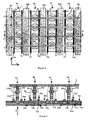
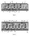
- the magnetoresistive random access memory shown in FIGS. 3 and 4 comprises not only the first column drivers 6ab and 6cd but, also, second column conductors 8a 8bc and 8d.
- the terminal of column 9b of each tunnel junction 10b of column 4b is then connected, via a transistor 16b, to the first column conductor 6ab and, via an additional transistor 11b, to the second conductor of column 8bc.
- the second column conductor 8bc is associated with both the column 4b and to a second adjacent column, in particular column 4c.
- the additional transistor 11b is provided with a gate 12b and a first gate 13b and second 14b electrodes.
- the gate 12b of the additional transistor 11b is connected to an additional grid conductor 15b.
- each cell 2 is connected via two transistors 11 and 16, to a first 6 and to a second 8 column driver.
- the grid conductors 7 and 15 are preferably parallel to the column conductors 6 and 8.
- Each second 8bc column conductor associated with a central column 4b, that is to say no located at the ends, is associated with another adjacent column 4c.
- an electric current passing through the tunnel junction 10b is divided into two fractions, respectively traversing the additional transistor 11b and the transistor 16b.
- Each fraction of current being much lower than the current crossing the junction 10b, the transistors 11b and 16b can be large significantly lower than the transistors used in a memory according to the art prior.
- the dimension of a transistor along a Y axis, parallel column drivers can be reduced by approximately 50% and thus the number of cells 2 can be substantially doubled per unit length of column along the Y axis.
- the additional transistors 11, the second column conductors 8 and additional grid conductors 15 require an increase in the order of 20% of the memory size along an X axis, perpendicular to the Y axis in the plane of the substrate 1, in applying current design rules of a CMOS-0.18 ⁇ m technology.
- the average surface area of a storage cell 2 can be reduced to 60% of the surface of a cell of a memory according to the prior art.
- a control device not shown, of conventional type, makes it possible to activate independently the two transistors 11b and 16b associated with a cell 2b.
- the current flowing through the junction 10b is smaller than the current of saturation of a transistor 11b or 16b, only one of these transistors (11b or 16b) can be enough.
- each tunnel junction 10d of the end column 4d is connected, via a transistor additional 11d to the second column driver 8d which is only associated with column 4d.
- the gate 12d of the additional transistor 11d is connected to an additional grid conductor 15d.
- a configuration analogue applies for the end column 4a, as shown in Figures 3 and 4.
- the two transistors 11b and 16b associated with the same cell 2b have, of preferably, a first common electrode 13b, as shown in FIG. figure 4.
- the two adjacent transistors 11b and 16c associated respectively to two adjacent cells 2b and 2c of a row 3 of cells 2 preferably have a second common electrode 14b.
- the corresponding column conductor 8bc integrates, preferably, the column of second electrodes 14b common.
- the first 13 and seconds 14 electrodes can respectively be the drain and the source transistors or vice versa.
- the magnetic tunnel junctions 10 are preferably connected to the corresponding line conductors 5 and transistors 11 and 16 associated by through interconnections 17 and metal layers 18.
- the interconnections 17 may comprise one or more layers disposed near the tunnel junction 10 and formed by a material having a low thermal conductivity, i.e. less than 5W / mK, which allows to confine the heat dissipated in the cell.
- Layer of material having a low thermal conductivity preferably has a low electrical resistivity, less than 100 ⁇ m, so that it represents a low resistance in series with the resistance of the tunnel junction 10.
- the writing of information in the memory shown in FIGS. be performed by spin injection. So the writing is based on the direction of the electrical current flowing through a cell during writing.
- This technique has the advantage of not requiring bulky drivers additional.
- the tunnel junction 10b of a cell 2b, the first electrode 13b, the interconnections 17 and the metal layers 18 associated with the cell 2b are preferably aligned along an axis Z perpendicular to the substrate 1.
- the memory comprises a plurality of drivers of current 19 parallel, electrically insulated magnetic tunnel junctions 10, each associated with a column 4 of cells 2 and arranged so as to ability to create a magnetic field at the location of tunnel junctions magnetic cells 2 of the associated column 4.
- Drivers of current 19 preferably comprise a ferromagnetic coating 20, example a soft magnetic material like an alloy of nickel and iron comprising 80% nickel and 20% iron. This alloy has a permeability magnetic field and a weak magnetic anisotropy, aligned, preferably, along the longitudinal axis of the current conductor 19.
- the coating ferromagnetic 20 covers at least one face of the current conductor 19 opposite the face opposite the junction 10, as shown in Figure 5. In FIG. 6, the coating also covers the lateral faces of the current conductor 19.
- the coating 20 allows the lines of magnetic field towards the tunnel junction 10, thus creating the same field only for an uncovered conductor, but with a lower current.
- a current flowing through a current conductor 19 creates a field magnetic device for defining a magnetization state of a tunnel junction 10 whose temperature is increased by Joule effect generated by a current of heating through the junction 10.
- the heating current is controlled by the voltages applied to the corresponding line driver 5, to the drivers gate 6 and 8 and the grid conductors 7 and 15 associated.
- the current is greater than the saturation current of a transistor 11 or 16, the two transistors 11 and 16 associated are used.
- the maximum value of the current of heating required during writing determines the size of transistors 11 and 16 and thus the number of cells 2 per column length unit along the Y axis.
- a current conductor 19 is arranged between magnetic tunnel junctions 10 of the associated 4 cell column and the substrate 1.
- the interconnections 17 between the tunnel junction 10 and the transistors 11 and 16 are then offset laterally with respect to the tunnel junction 10 and to the corresponding current conductor 19, which are aligned along the Z axis.
- current conductors 19 are preferably arranged very close to the junctions tunnel 10 to maximize the magnetic field acting on the junctions 10.
- the current flowing through a current conductor 19 generates heat by Joule effect in the current conductor 19, which allows further heat the tunnel junction 10 when writing or at least reduce thermal losses.
- the resistivity of the material of the conductors of current 19 is chosen to maximize the Joule effect, without, however, exceed an appropriate maximum voltage.
- two adjacent magnetic tunnel junctions 10a and 10b of a line of cells 3 are connected to the associated line conductor 5 by through a common metal layer 21ab and by a common interconnection 22ab.
- the common metal layer 21 (21ab, 21cd) is preferably constituted by a material having electrical conductivity high, for example by copper or aluminum. So when both corresponding junctions 10a and 10b are simultaneously traversed by respective electrical currents, the heat dissipated in the interconnection common 22ab is proportional to the square of the sum of the currents which allows to further heat the tunnel junctions during the writing phases without increasing the heating current passing through each tunnel junction 10.
- the number of adjacent magnetic tunnel junctions 10 grouped by via a common metallic layer 21 and by an interconnection common 22 may be greater than two and chosen, in combination with the resistor Rv of the common interconnection 22, so that the heat dissipated in the common interconnection 22 be comparable to the heat dissipated in junction 10. It is possible to write in a cell or in several cells simultaneously.
- the memory preferably comprises, as shown, by way of example, in FIG. 5, a sealing insulating material 23 covering at least the matrix of cells 2, the column conductors 6 and 8 and the current conductors 19 and can even coat the line conductors 5 as shown in Figure 6.
- the insulating material 23 of sealing has a low thermal conductivity allowing, during a heat-assisted writing step, to confine the heat and thus obtain a given increased temperature with a reduced heating current.
- the insulating material 23 is, for example, SiO 2 silica whose thermal conductivity is 1.4W / mK.
Landscapes
- Engineering & Computer Science (AREA)
- Chemical & Material Sciences (AREA)
- Nanotechnology (AREA)
- Computer Hardware Design (AREA)
- Physics & Mathematics (AREA)
- Mathematical Physics (AREA)
- Theoretical Computer Science (AREA)
- Crystallography & Structural Chemistry (AREA)
- Mram Or Spin Memory Techniques (AREA)
- Semiconductor Memories (AREA)
- Hall/Mr Elements (AREA)
Abstract
Description
Claims (16)
- Mémoire vive magnétorésistive comportant, sur un substrat semiconducteur (1), une matrice de cellules (2) agencées en lignes (3) et en colonnes (4) et destinées chacune à stocker un bit d'information, chaque cellule (2b) d'une colonne (4b) comportant une jonction tunnel magnétique (10b) ayant une borne de ligne et une borne de colonne (9b) reliées respectivement à un conducteur de ligne (5) et, par l'intermédiaire d'un transistor (16b), muni d'une grille et de première (13b) et seconde électrodes, à un premier conducteur de colonne (6ab), associé à ladite colonne (4b) et à une première colonne adjacente (4a), la grille du transistor étant connectée à un conducteur de grille (7b), mémoire caractérisée en ce que la borne de colonne (9b) de chaque jonction tunnel (10b) d'une colonne (4b) est connectée, par l'intermédiaire d'un transistor supplémentaire (11b), muni d'une grille (12b) et de première (13b) et seconde électrodes (14b), à un second conducteur de colonne (8bc), la grille (12b) du transistor supplémentaire (11b) étant connectée à un conducteur de grille supplémentaire (15b).
- Mémoire selon la revendication 1, caractérisée en ce que, la matrice de cellules (2) comportant des colonnes centrales (4b) et deux colonnes d'extrémité (4a, 4d), le second conducteur (8bc) de chaque colonne centrale (4b) est associé à ladite colonne (4b) et à une seconde colonne adjacente (4c).
- Mémoire selon l'une des revendications 1 et 2, caractérisée en ce que les conducteurs de grille (7, 15) sont parallèles au conducteur de colonne (6, 8).
- Mémoire selon l'une quelconque des revendications 1 à 3, caractérisée en ce que les deux transistors (16b, 11b) associés à une cellule (2b) ont une première électrode (13b) commune.
- Mémoire selon l'une quelconque des revendications 1 à 4, caractérisée en ce que deux transistors adjacents (11 b, 16c) associés respectivement à deux cellules adjacentes (2b, 2c) d'une ligne (3) de cellules (2) ont une seconde électrode (14b) commune.
- Mémoire selon la revendication 5, caractérisée en ce qu'un conducteur de colonne (8bc) intègre une colonne de secondes électrodes (14b) communes.
- Mémoire selon l'une quelconque des revendications 1 à 6, caractérisée en ce qu'une jonction tunnel magnétique (10) est connectée au conducteur de ligne (5) correspondant et aux transistors (11, 16) associés par l'intermédiaire d'interconnexions (17) et de couches métalliques (18).
- Mémoire selon la revendication 7, caractérisée en ce que les interconnexions (17) comportent une couche de matériau ayant une conductivité thermique faible.
- Mémoire selon l'une des revendications 6 et 7, caractérisée en ce que la jonction tunnel magnétique (10) d'une cellule (2), une électrode (13) de transistor, les interconnexions (17) et les couches métalliques (18) associées sont alignées selon un axe (Z) perpendiculaire au substrat (1).
- Mémoire selon l'une quelconque des revendications 1 à 8, caractérisée en ce qu'elle comporte une pluralité de conducteurs de courant (19) parallèles, isolés électriquement des jonctions tunnel magnétiques (10), associés chacun à une colonne (4) de cellules (2) et disposés de manière à pouvoir créer un champ magnétique à l'emplacement des jonctions tunnel magnétiques (10) des cellules (2) de la colonne (4) associée.
- Mémoire selon la revendication 10, caractérisée en ce qu'un conducteur de courant (19) comporte un revêtement ferromagnétique (20).
- Mémoire selon l'une des revendications 10 et 11, caractérisée en ce qu'un conducteur de courant (19) est disposé entre les jonctions tunnel magnétiques (10) de la colonne (4) de cellules (2) associée et le substrat (1).
- Mémoire selon l'une quelconque des revendication 1 à 8 et 10 à 12, caractérisée en ce qu'au moins deux jonctions tunnel magnétiques (10a, 10b) adjacentes d'une ligne (3) de cellules (2) sont connectées au conducteur de ligne (5) par l'intermédiaire d'une couche métallique commune (21ab) et par une interconnexion commune (22ab).
- Mémoire selon la revendication 13, caractérisée en ce que la couche métallique commune (21ab) est constituée par un matériau ayant une conductivité électrique élevée.
- Mémoire selon l'une quelconque des revendications 1 à 14, caractérisée en ce qu'elle comporte un matériau isolant (23) de scellement ayant une conductivité thermique faible et recouvrant au moins la matrice de cellules (2) et les conducteurs de colonne (6, 8).
- Mémoire selon la revendication 15, caractérisée en ce que le matériau isolant (23) de scellement recouvre les conducteurs de ligne (5).
Applications Claiming Priority (2)
| Application Number | Priority Date | Filing Date | Title |
|---|---|---|---|
| FR0402354A FR2867300B1 (fr) | 2004-03-05 | 2004-03-05 | Memoire vive magnetoresistive a haute densite de courant |
| FR0402354 | 2004-03-05 |
Publications (2)
| Publication Number | Publication Date |
|---|---|
| EP1580760A1 true EP1580760A1 (fr) | 2005-09-28 |
| EP1580760B1 EP1580760B1 (fr) | 2011-04-06 |
Family
ID=34855105
Family Applications (1)
| Application Number | Title | Priority Date | Filing Date |
|---|---|---|---|
| EP05354008A Expired - Lifetime EP1580760B1 (fr) | 2004-03-05 | 2005-02-22 | Mémoire vive magnétorésistive à haute densité de courant |
Country Status (6)
| Country | Link |
|---|---|
| US (1) | US7626221B2 (fr) |
| EP (1) | EP1580760B1 (fr) |
| JP (1) | JP4749743B2 (fr) |
| AT (1) | ATE504922T1 (fr) |
| DE (1) | DE602005027285D1 (fr) |
| FR (1) | FR2867300B1 (fr) |
Families Citing this family (8)
| Publication number | Priority date | Publication date | Assignee | Title |
|---|---|---|---|---|
| JP4573042B2 (ja) | 2004-09-27 | 2010-11-04 | セイコーエプソン株式会社 | 薄板状体をセット可能なトレイ、記録装置 |
| TWI449040B (zh) * | 2006-10-06 | 2014-08-11 | Crocus Technology Sa | 用於提供內容可定址的磁阻式隨機存取記憶體單元之系統及方法 |
| ATE538474T1 (de) * | 2008-04-07 | 2012-01-15 | Crocus Technology Sa | System und verfahren zum schreiben von daten auf magnetoresistive direktzugriffsspeicherzellen |
| EP2124228B1 (fr) | 2008-05-20 | 2014-03-05 | Crocus Technology | Mémoire à accès aléatoire magnétique avec une jonction elliptique |
| US8031519B2 (en) | 2008-06-18 | 2011-10-04 | Crocus Technology S.A. | Shared line magnetic random access memory cells |
| JP5502635B2 (ja) * | 2010-03-08 | 2014-05-28 | 株式会社東芝 | 半導体記憶装置 |
| EP3910634A4 (fr) * | 2019-01-30 | 2022-01-05 | Huawei Technologies Co., Ltd. | Mémoire et dispositif électronique |
| JP2023037504A (ja) * | 2021-09-03 | 2023-03-15 | キオクシア株式会社 | 磁気メモリ |
Citations (5)
| Publication number | Priority date | Publication date | Assignee | Title |
|---|---|---|---|---|
| US20030031045A1 (en) * | 2001-08-08 | 2003-02-13 | Keiji Hosotani | Magnetic random access memory including memory cell unit and reference cell unit |
| US20030086313A1 (en) * | 2001-11-07 | 2003-05-08 | Yoshiaki Asao | Magnetic memory device using SOI substrate and method of manufacturing the same |
| US20030189853A1 (en) * | 2002-04-03 | 2003-10-09 | Mitsubishi Denki Kabushiki Kaisha, Mitsubishi Electric Engineering Company Limited | Thin film magnetic memory device provided with a dummy cell for data read reference |
| JP2003298025A (ja) * | 2002-03-29 | 2003-10-17 | Toshiba Corp | 磁気記憶装置 |
| WO2004057619A1 (fr) * | 2002-12-20 | 2004-07-08 | Infineon Technologies Ag | Amplificateur de detection de courant |
Family Cites Families (12)
| Publication number | Priority date | Publication date | Assignee | Title |
|---|---|---|---|---|
| US6272041B1 (en) * | 2000-08-28 | 2001-08-07 | Motorola, Inc. | MTJ MRAM parallel-parallel architecture |
| KR100403313B1 (ko) * | 2001-05-22 | 2003-10-30 | 주식회사 하이닉스반도체 | 바이폴라 접합 트랜지스터를 이용한 마그네틱 램 및 그형성방법 |
| JP3844117B2 (ja) * | 2001-06-27 | 2006-11-08 | インターナショナル・ビジネス・マシーンズ・コーポレーション | メモリセル、記憶回路ブロック、データの書き込み方法及びデータの読み出し方法 |
| JP2003209228A (ja) * | 2001-11-07 | 2003-07-25 | Toshiba Corp | 磁気記憶装置及びその製造方法 |
| FR2832542B1 (fr) * | 2001-11-16 | 2005-05-06 | Commissariat Energie Atomique | Dispositif magnetique a jonction tunnel magnetique, memoire et procedes d'ecriture et de lecture utilisant ce dispositif |
| JP4047615B2 (ja) * | 2002-04-03 | 2008-02-13 | 株式会社ルネサステクノロジ | 磁気記憶装置 |
| US6621730B1 (en) * | 2002-08-27 | 2003-09-16 | Motorola, Inc. | Magnetic random access memory having a vertical write line |
| JP4266297B2 (ja) * | 2002-09-05 | 2009-05-20 | 株式会社ルネサステクノロジ | 不揮発性記憶装置 |
| JP2004110992A (ja) * | 2002-09-20 | 2004-04-08 | Renesas Technology Corp | 薄膜磁性体記憶装置 |
| US6944049B2 (en) * | 2002-10-30 | 2005-09-13 | Infineon Technologies Ag | Magnetic tunnel junction memory cell architecture |
| JP3888463B2 (ja) * | 2002-11-27 | 2007-03-07 | 日本電気株式会社 | メモリセル及び磁気ランダムアクセスメモリ |
| US6980466B2 (en) * | 2004-01-15 | 2005-12-27 | Hewlett-Packard Development Company, L.P. | Soft-reference four conductor magnetic memory storage device |
-
2004
- 2004-03-05 FR FR0402354A patent/FR2867300B1/fr not_active Expired - Fee Related
-
2005
- 2005-02-22 AT AT05354008T patent/ATE504922T1/de not_active IP Right Cessation
- 2005-02-22 DE DE602005027285T patent/DE602005027285D1/de not_active Expired - Lifetime
- 2005-02-22 EP EP05354008A patent/EP1580760B1/fr not_active Expired - Lifetime
- 2005-02-23 US US11/062,926 patent/US7626221B2/en not_active Expired - Lifetime
- 2005-03-07 JP JP2005062739A patent/JP4749743B2/ja not_active Expired - Fee Related
Patent Citations (5)
| Publication number | Priority date | Publication date | Assignee | Title |
|---|---|---|---|---|
| US20030031045A1 (en) * | 2001-08-08 | 2003-02-13 | Keiji Hosotani | Magnetic random access memory including memory cell unit and reference cell unit |
| US20030086313A1 (en) * | 2001-11-07 | 2003-05-08 | Yoshiaki Asao | Magnetic memory device using SOI substrate and method of manufacturing the same |
| JP2003298025A (ja) * | 2002-03-29 | 2003-10-17 | Toshiba Corp | 磁気記憶装置 |
| US20030189853A1 (en) * | 2002-04-03 | 2003-10-09 | Mitsubishi Denki Kabushiki Kaisha, Mitsubishi Electric Engineering Company Limited | Thin film magnetic memory device provided with a dummy cell for data read reference |
| WO2004057619A1 (fr) * | 2002-12-20 | 2004-07-08 | Infineon Technologies Ag | Amplificateur de detection de courant |
Also Published As
| Publication number | Publication date |
|---|---|
| US7626221B2 (en) | 2009-12-01 |
| ATE504922T1 (de) | 2011-04-15 |
| FR2867300B1 (fr) | 2006-04-28 |
| JP2005251382A (ja) | 2005-09-15 |
| EP1580760B1 (fr) | 2011-04-06 |
| JP4749743B2 (ja) | 2011-08-17 |
| US20050195658A1 (en) | 2005-09-08 |
| DE602005027285D1 (de) | 2011-05-19 |
| FR2867300A1 (fr) | 2005-09-09 |
Similar Documents
| Publication | Publication Date | Title |
|---|---|---|
| US6584029B2 (en) | One-time programmable memory using fuse/anti-fuse and vertically oriented fuse unit memory cells | |
| EP2633525B1 (fr) | Element magnetique inscriptible. | |
| EP2140455B1 (fr) | Memoire magnetique a jonction tunnel magnetique | |
| EP2599138B1 (fr) | Element magnetique inscriptible | |
| EP2073210B1 (fr) | Mémoire magnétique à écriture assistée thermiquement | |
| EP1438722B1 (fr) | Memoire magnetique a selection a l'ecriture par inhibition et procede pour son ecriture | |
| EP2255362B1 (fr) | Element magnetique a ecriture assistee thermiquement | |
| US20050083760A1 (en) | Magnetoresistive random access memory (MRAM) cell having a diode with asymmetrical characteristics | |
| WO2005086171A1 (fr) | Memoire magnetique a jonction tunnel magnetique a ecriture assistee thermiquement et procede pour son ecriture | |
| TWI260630B (en) | Magnetic tunnel junction memory cell architecture | |
| US6930369B2 (en) | Thin film device and a method of providing thermal assistance therein | |
| CN1433022A (zh) | 高密度磁随机存取存储器及其操作方法 | |
| US20090251950A1 (en) | Integrated Circuit, Memory Cell Arrangement, Thermal Select Magneto-Resistive Memory Cell, Method of Operating a Thermal Select Magneto-Resistive Memory Cell, and Method of Manufacturing a Thermal Select Magneto-Resistive Memory Cell | |
| WO2016113503A1 (fr) | Point mémoire magnétique | |
| KR20030074459A (ko) | 데이터 저장 디바이스 및 그 제조 프로세스 | |
| US7593278B2 (en) | Memory element with thermoelectric pulse | |
| EP1580760B1 (fr) | Mémoire vive magnétorésistive à haute densité de courant | |
| CN113574693A (zh) | 半导体装置和包括半导体装置的电子设备 | |
| CN103871464B (zh) | 可程序编辑电阻元件记忆体、操作方法及电子系统 | |
| EP3788656A1 (fr) | Limiteur de courant supraconducteur avec entretoise électriquement conductrice | |
| US7787289B2 (en) | MRAM design with local write conductors of reduced cross-sectional area | |
| JP2005123628A (ja) | 磁気メモリデバイス | |
| KR20060039781A (ko) | 발열체를 갖는 자기 램 소자의 구동 방법들 | |
| FR3131438A1 (fr) | Ensemble comprenant au moins deux sélecteurs et deux mémoires résistives non-volatiles, matrice et procédé de fabrication associés | |
| FR3131437A1 (fr) | Ensemble comprenant au moins deux mémoires résistives non-volatiles et deux sélecteurs, matrice et procédé de fabrication associés |
Legal Events
| Date | Code | Title | Description |
|---|---|---|---|
| PUAI | Public reference made under article 153(3) epc to a published international application that has entered the european phase |
Free format text: ORIGINAL CODE: 0009012 |
|
| AK | Designated contracting states |
Kind code of ref document: A1 Designated state(s): AT BE BG CH CY CZ DE DK EE ES FI FR GB GR HU IE IS IT LI LT LU MC NL PL PT RO SE SI SK TR |
|
| AX | Request for extension of the european patent |
Extension state: AL BA HR LV MK YU |
|
| 17P | Request for examination filed |
Effective date: 20060128 |
|
| AKX | Designation fees paid |
Designated state(s): AT BE BG CH CY CZ DE DK EE ES FI FR GB GR HU IE IS IT LI LT LU MC NL PL PT RO SE SI SK TR |
|
| 17Q | First examination report despatched |
Effective date: 20061205 |
|
| 17Q | First examination report despatched |
Effective date: 20061205 |
|
| GRAP | Despatch of communication of intention to grant a patent |
Free format text: ORIGINAL CODE: EPIDOSNIGR1 |
|
| RAP1 | Party data changed (applicant data changed or rights of an application transferred) |
Owner name: CENTRE NATIONAL DE LA RECHERCHE SCIENTIFIQUE Owner name: COMMISSARIAT A L'ENERGIE ATOMIQUE ET AUX ENERGIES |
|
| GRAS | Grant fee paid |
Free format text: ORIGINAL CODE: EPIDOSNIGR3 |
|
| GRAA | (expected) grant |
Free format text: ORIGINAL CODE: 0009210 |
|
| AK | Designated contracting states |
Kind code of ref document: B1 Designated state(s): AT BE BG CH CY CZ DE DK EE ES FI FR GB GR HU IE IS IT LI LT LU MC NL PL PT RO SE SI SK TR |
|
| REG | Reference to a national code |
Ref country code: GB Ref legal event code: FG4D Free format text: NOT ENGLISH |
|
| REG | Reference to a national code |
Ref country code: CH Ref legal event code: EP |
|
| REG | Reference to a national code |
Ref country code: IE Ref legal event code: FG4D |
|
| REF | Corresponds to: |
Ref document number: 602005027285 Country of ref document: DE Date of ref document: 20110519 Kind code of ref document: P |
|
| REG | Reference to a national code |
Ref country code: DE Ref legal event code: R096 Ref document number: 602005027285 Country of ref document: DE Effective date: 20110519 |
|
| REG | Reference to a national code |
Ref country code: NL Ref legal event code: VDEP Effective date: 20110406 |
|
| PG25 | Lapsed in a contracting state [announced via postgrant information from national office to epo] |
Ref country code: SI Free format text: LAPSE BECAUSE OF FAILURE TO SUBMIT A TRANSLATION OF THE DESCRIPTION OR TO PAY THE FEE WITHIN THE PRESCRIBED TIME-LIMIT Effective date: 20110406 |
|
| LTIE | Lt: invalidation of european patent or patent extension |
Effective date: 20110406 |
|
| REG | Reference to a national code |
Ref country code: IE Ref legal event code: FD4D |
|
| PG25 | Lapsed in a contracting state [announced via postgrant information from national office to epo] |
Ref country code: SE Free format text: LAPSE BECAUSE OF FAILURE TO SUBMIT A TRANSLATION OF THE DESCRIPTION OR TO PAY THE FEE WITHIN THE PRESCRIBED TIME-LIMIT Effective date: 20110406 Ref country code: LT Free format text: LAPSE BECAUSE OF FAILURE TO SUBMIT A TRANSLATION OF THE DESCRIPTION OR TO PAY THE FEE WITHIN THE PRESCRIBED TIME-LIMIT Effective date: 20110406 Ref country code: PT Free format text: LAPSE BECAUSE OF FAILURE TO SUBMIT A TRANSLATION OF THE DESCRIPTION OR TO PAY THE FEE WITHIN THE PRESCRIBED TIME-LIMIT Effective date: 20110808 |
|
| PG25 | Lapsed in a contracting state [announced via postgrant information from national office to epo] |
Ref country code: ES Free format text: LAPSE BECAUSE OF FAILURE TO SUBMIT A TRANSLATION OF THE DESCRIPTION OR TO PAY THE FEE WITHIN THE PRESCRIBED TIME-LIMIT Effective date: 20110717 Ref country code: CY Free format text: LAPSE BECAUSE OF FAILURE TO SUBMIT A TRANSLATION OF THE DESCRIPTION OR TO PAY THE FEE WITHIN THE PRESCRIBED TIME-LIMIT Effective date: 20110406 Ref country code: GR Free format text: LAPSE BECAUSE OF FAILURE TO SUBMIT A TRANSLATION OF THE DESCRIPTION OR TO PAY THE FEE WITHIN THE PRESCRIBED TIME-LIMIT Effective date: 20110707 Ref country code: AT Free format text: LAPSE BECAUSE OF FAILURE TO SUBMIT A TRANSLATION OF THE DESCRIPTION OR TO PAY THE FEE WITHIN THE PRESCRIBED TIME-LIMIT Effective date: 20110406 Ref country code: IS Free format text: LAPSE BECAUSE OF FAILURE TO SUBMIT A TRANSLATION OF THE DESCRIPTION OR TO PAY THE FEE WITHIN THE PRESCRIBED TIME-LIMIT Effective date: 20110806 Ref country code: FI Free format text: LAPSE BECAUSE OF FAILURE TO SUBMIT A TRANSLATION OF THE DESCRIPTION OR TO PAY THE FEE WITHIN THE PRESCRIBED TIME-LIMIT Effective date: 20110406 |
|
| PG25 | Lapsed in a contracting state [announced via postgrant information from national office to epo] |
Ref country code: NL Free format text: LAPSE BECAUSE OF FAILURE TO SUBMIT A TRANSLATION OF THE DESCRIPTION OR TO PAY THE FEE WITHIN THE PRESCRIBED TIME-LIMIT Effective date: 20110406 |
|
| PG25 | Lapsed in a contracting state [announced via postgrant information from national office to epo] |
Ref country code: IE Free format text: LAPSE BECAUSE OF FAILURE TO SUBMIT A TRANSLATION OF THE DESCRIPTION OR TO PAY THE FEE WITHIN THE PRESCRIBED TIME-LIMIT Effective date: 20110406 Ref country code: CZ Free format text: LAPSE BECAUSE OF FAILURE TO SUBMIT A TRANSLATION OF THE DESCRIPTION OR TO PAY THE FEE WITHIN THE PRESCRIBED TIME-LIMIT Effective date: 20110406 Ref country code: EE Free format text: LAPSE BECAUSE OF FAILURE TO SUBMIT A TRANSLATION OF THE DESCRIPTION OR TO PAY THE FEE WITHIN THE PRESCRIBED TIME-LIMIT Effective date: 20110406 |
|
| PLBE | No opposition filed within time limit |
Free format text: ORIGINAL CODE: 0009261 |
|
| STAA | Information on the status of an ep patent application or granted ep patent |
Free format text: STATUS: NO OPPOSITION FILED WITHIN TIME LIMIT |
|
| PG25 | Lapsed in a contracting state [announced via postgrant information from national office to epo] |
Ref country code: DK Free format text: LAPSE BECAUSE OF FAILURE TO SUBMIT A TRANSLATION OF THE DESCRIPTION OR TO PAY THE FEE WITHIN THE PRESCRIBED TIME-LIMIT Effective date: 20110406 Ref country code: PL Free format text: LAPSE BECAUSE OF FAILURE TO SUBMIT A TRANSLATION OF THE DESCRIPTION OR TO PAY THE FEE WITHIN THE PRESCRIBED TIME-LIMIT Effective date: 20110406 Ref country code: RO Free format text: LAPSE BECAUSE OF FAILURE TO SUBMIT A TRANSLATION OF THE DESCRIPTION OR TO PAY THE FEE WITHIN THE PRESCRIBED TIME-LIMIT Effective date: 20110406 Ref country code: SK Free format text: LAPSE BECAUSE OF FAILURE TO SUBMIT A TRANSLATION OF THE DESCRIPTION OR TO PAY THE FEE WITHIN THE PRESCRIBED TIME-LIMIT Effective date: 20110406 |
|
| 26N | No opposition filed |
Effective date: 20120110 |
|
| REG | Reference to a national code |
Ref country code: DE Ref legal event code: R097 Ref document number: 602005027285 Country of ref document: DE Effective date: 20120110 |
|
| BERE | Be: lapsed |
Owner name: COMMISSARIAT A L'ENERGIE ATOMIQUE ET AUX ENERGIES Effective date: 20120228 Owner name: CENTRE NATIONAL DE LA RECHERCHE SCIENTIFIQUE Effective date: 20120228 |
|
| PG25 | Lapsed in a contracting state [announced via postgrant information from national office to epo] |
Ref country code: MC Free format text: LAPSE BECAUSE OF NON-PAYMENT OF DUE FEES Effective date: 20120229 |
|
| REG | Reference to a national code |
Ref country code: CH Ref legal event code: PL |
|
| PG25 | Lapsed in a contracting state [announced via postgrant information from national office to epo] |
Ref country code: CH Free format text: LAPSE BECAUSE OF NON-PAYMENT OF DUE FEES Effective date: 20120229 Ref country code: LI Free format text: LAPSE BECAUSE OF NON-PAYMENT OF DUE FEES Effective date: 20120229 |
|
| PG25 | Lapsed in a contracting state [announced via postgrant information from national office to epo] |
Ref country code: BE Free format text: LAPSE BECAUSE OF NON-PAYMENT OF DUE FEES Effective date: 20120228 |
|
| PG25 | Lapsed in a contracting state [announced via postgrant information from national office to epo] |
Ref country code: BG Free format text: LAPSE BECAUSE OF FAILURE TO SUBMIT A TRANSLATION OF THE DESCRIPTION OR TO PAY THE FEE WITHIN THE PRESCRIBED TIME-LIMIT Effective date: 20110706 |
|
| PG25 | Lapsed in a contracting state [announced via postgrant information from national office to epo] |
Ref country code: TR Free format text: LAPSE BECAUSE OF FAILURE TO SUBMIT A TRANSLATION OF THE DESCRIPTION OR TO PAY THE FEE WITHIN THE PRESCRIBED TIME-LIMIT Effective date: 20110406 |
|
| PG25 | Lapsed in a contracting state [announced via postgrant information from national office to epo] |
Ref country code: LU Free format text: LAPSE BECAUSE OF NON-PAYMENT OF DUE FEES Effective date: 20120222 |
|
| PG25 | Lapsed in a contracting state [announced via postgrant information from national office to epo] |
Ref country code: HU Free format text: LAPSE BECAUSE OF FAILURE TO SUBMIT A TRANSLATION OF THE DESCRIPTION OR TO PAY THE FEE WITHIN THE PRESCRIBED TIME-LIMIT Effective date: 20050222 |
|
| REG | Reference to a national code |
Ref country code: FR Ref legal event code: PLFP Year of fee payment: 12 |
|
| REG | Reference to a national code |
Ref country code: FR Ref legal event code: PLFP Year of fee payment: 13 |
|
| REG | Reference to a national code |
Ref country code: FR Ref legal event code: PLFP Year of fee payment: 14 |
|
| PGFP | Annual fee paid to national office [announced via postgrant information from national office to epo] |
Ref country code: IT Payment date: 20200211 Year of fee payment: 16 |
|
| PGFP | Annual fee paid to national office [announced via postgrant information from national office to epo] |
Ref country code: FR Payment date: 20210226 Year of fee payment: 17 |
|
| PGFP | Annual fee paid to national office [announced via postgrant information from national office to epo] |
Ref country code: DE Payment date: 20210209 Year of fee payment: 17 Ref country code: GB Payment date: 20210216 Year of fee payment: 17 |
|
| PG25 | Lapsed in a contracting state [announced via postgrant information from national office to epo] |
Ref country code: IT Free format text: LAPSE BECAUSE OF NON-PAYMENT OF DUE FEES Effective date: 20210222 |
|
| REG | Reference to a national code |
Ref country code: DE Ref legal event code: R119 Ref document number: 602005027285 Country of ref document: DE |
|
| GBPC | Gb: european patent ceased through non-payment of renewal fee |
Effective date: 20220222 |
|
| PG25 | Lapsed in a contracting state [announced via postgrant information from national office to epo] |
Ref country code: FR Free format text: LAPSE BECAUSE OF NON-PAYMENT OF DUE FEES Effective date: 20220228 |
|
| PG25 | Lapsed in a contracting state [announced via postgrant information from national office to epo] |
Ref country code: GB Free format text: LAPSE BECAUSE OF NON-PAYMENT OF DUE FEES Effective date: 20220222 Ref country code: DE Free format text: LAPSE BECAUSE OF NON-PAYMENT OF DUE FEES Effective date: 20220901 |