EP1577992B1 - Semiconductor laser assembly - Google Patents
Semiconductor laser assembly Download PDFInfo
- Publication number
- EP1577992B1 EP1577992B1 EP03786367A EP03786367A EP1577992B1 EP 1577992 B1 EP1577992 B1 EP 1577992B1 EP 03786367 A EP03786367 A EP 03786367A EP 03786367 A EP03786367 A EP 03786367A EP 1577992 B1 EP1577992 B1 EP 1577992B1
- Authority
- EP
- European Patent Office
- Prior art keywords
- submount
- heatsink
- laser diode
- groove
- solder
- Prior art date
- Legal status (The legal status is an assumption and is not a legal conclusion. Google has not performed a legal analysis and makes no representation as to the accuracy of the status listed.)
- Expired - Fee Related
Links
Images


Classifications
-
- H—ELECTRICITY
- H01—ELECTRIC ELEMENTS
- H01S—DEVICES USING THE PROCESS OF LIGHT AMPLIFICATION BY STIMULATED EMISSION OF RADIATION [LASER] TO AMPLIFY OR GENERATE LIGHT; DEVICES USING STIMULATED EMISSION OF ELECTROMAGNETIC RADIATION IN WAVE RANGES OTHER THAN OPTICAL
- H01S5/00—Semiconductor lasers
- H01S5/02—Structural details or components not essential to laser action
- H01S5/022—Mountings; Housings
- H01S5/0233—Mounting configuration of laser chips
-
- H—ELECTRICITY
- H01—ELECTRIC ELEMENTS
- H01S—DEVICES USING THE PROCESS OF LIGHT AMPLIFICATION BY STIMULATED EMISSION OF RADIATION [LASER] TO AMPLIFY OR GENERATE LIGHT; DEVICES USING STIMULATED EMISSION OF ELECTROMAGNETIC RADIATION IN WAVE RANGES OTHER THAN OPTICAL
- H01S5/00—Semiconductor lasers
- H01S5/02—Structural details or components not essential to laser action
- H01S5/022—Mountings; Housings
- H01S5/023—Mount members, e.g. sub-mount members
-
- H—ELECTRICITY
- H01—ELECTRIC ELEMENTS
- H01S—DEVICES USING THE PROCESS OF LIGHT AMPLIFICATION BY STIMULATED EMISSION OF RADIATION [LASER] TO AMPLIFY OR GENERATE LIGHT; DEVICES USING STIMULATED EMISSION OF ELECTROMAGNETIC RADIATION IN WAVE RANGES OTHER THAN OPTICAL
- H01S5/00—Semiconductor lasers
- H01S5/02—Structural details or components not essential to laser action
- H01S5/022—Mountings; Housings
- H01S5/0235—Method for mounting laser chips
- H01S5/02375—Positioning of the laser chips
-
- H—ELECTRICITY
- H01—ELECTRIC ELEMENTS
- H01L—SEMICONDUCTOR DEVICES NOT COVERED BY CLASS H10
- H01L2224/00—Indexing scheme for arrangements for connecting or disconnecting semiconductor or solid-state bodies and methods related thereto as covered by H01L24/00
- H01L2224/01—Means for bonding being attached to, or being formed on, the surface to be connected, e.g. chip-to-package, die-attach, "first-level" interconnects; Manufacturing methods related thereto
- H01L2224/42—Wire connectors; Manufacturing methods related thereto
- H01L2224/47—Structure, shape, material or disposition of the wire connectors after the connecting process
- H01L2224/48—Structure, shape, material or disposition of the wire connectors after the connecting process of an individual wire connector
- H01L2224/4805—Shape
- H01L2224/4809—Loop shape
- H01L2224/48091—Arched
-
- H—ELECTRICITY
- H01—ELECTRIC ELEMENTS
- H01L—SEMICONDUCTOR DEVICES NOT COVERED BY CLASS H10
- H01L2224/00—Indexing scheme for arrangements for connecting or disconnecting semiconductor or solid-state bodies and methods related thereto as covered by H01L24/00
- H01L2224/01—Means for bonding being attached to, or being formed on, the surface to be connected, e.g. chip-to-package, die-attach, "first-level" interconnects; Manufacturing methods related thereto
- H01L2224/42—Wire connectors; Manufacturing methods related thereto
- H01L2224/47—Structure, shape, material or disposition of the wire connectors after the connecting process
- H01L2224/49—Structure, shape, material or disposition of the wire connectors after the connecting process of a plurality of wire connectors
- H01L2224/491—Disposition
- H01L2224/4912—Layout
- H01L2224/49175—Parallel arrangements
-
- H—ELECTRICITY
- H01—ELECTRIC ELEMENTS
- H01S—DEVICES USING THE PROCESS OF LIGHT AMPLIFICATION BY STIMULATED EMISSION OF RADIATION [LASER] TO AMPLIFY OR GENERATE LIGHT; DEVICES USING STIMULATED EMISSION OF ELECTROMAGNETIC RADIATION IN WAVE RANGES OTHER THAN OPTICAL
- H01S5/00—Semiconductor lasers
- H01S5/02—Structural details or components not essential to laser action
- H01S5/022—Mountings; Housings
- H01S5/0235—Method for mounting laser chips
- H01S5/02355—Fixing laser chips on mounts
- H01S5/0237—Fixing laser chips on mounts by soldering
-
- H—ELECTRICITY
- H01—ELECTRIC ELEMENTS
- H01S—DEVICES USING THE PROCESS OF LIGHT AMPLIFICATION BY STIMULATED EMISSION OF RADIATION [LASER] TO AMPLIFY OR GENERATE LIGHT; DEVICES USING STIMULATED EMISSION OF ELECTROMAGNETIC RADIATION IN WAVE RANGES OTHER THAN OPTICAL
- H01S5/00—Semiconductor lasers
- H01S5/02—Structural details or components not essential to laser action
- H01S5/024—Arrangements for thermal management
- H01S5/02469—Passive cooling, e.g. where heat is removed by the housing as a whole or by a heat pipe without any active cooling element like a TEC
Definitions
- the present invention relates to a laser diode assembly having a structure wherein a laser diode device is jointed to a heatsink with a submount in between or directly.
- the invention relates to a laser diode assembly comprising a construction wherein in assembly, solder overflow from a solder joint face between a laser diode device and a submount or a heatsink is inhibited, and overflowing solder does not form bulb-shaped solder residue on the laser diode device, the submount, or the heatsink.
- a so-called laser diode assembly wherein a substrate side of a laser diode device is jointed to a heatsink directly or with a submount in between through a solder layer is manufactured as a produce.
- a laser diode device 12 is jointed to a submount 16 through a first solder layer 14, and the submount 16 is jointed to a heatsink 20 through a second solder layer 18.
- the laser diode device 12 comprises a lamination structure including a light-emitting layer on a semiconductor substrate. There is a structure wherein the laser diode 12 is directly jointed to the heatsink 20 without the submount 16.
- the heatsink 20 is provided with an electrode pad 24 with an insulating plate 22 in between.
- the electrode pad 24 and an electrode of the laser diode device 12 are connected (wire bonded) through a wire 26. That is, the laser diode device 12 is connected to outer equipment through the electrode pad 24.
- the laser diode device 12 is, for example, a GaAs edge-emitting type laser diode device formed on a GaAs substrate.
- an end face opposite of the electrode pad 24 side is an emitting end face.
- Number of the laser diode device 12 can be one as shown in Fig. 7 or plural. Some of the laser diode device 12 are arranged in the shape of an array.
- the submount 16 is a part to reinforce mechanical strength of the laser diode device 12 and is a metal plate made of, for example, silicon carbide (SiC) or an alloy of copper (Cu) and tungsten (W).
- the heatsink 20 is often made of a copper plate.
- the first solder layer 14 to joint the laser diode device 12 and the submount 16 is, for example, a gold-tin (Au/Sn) solder layer.
- the second solder layer 18 to joint the submount 16 and the heatsink 20 is, for example, an indium (In) solder layer.
- the submount 16 which lays the laser diode device 12 on a gold-tin solder plating layer formed on a joint face of the submount 16 is forwarded into a reflow oven, and heated to a melting temperature of the gold-tin solder or higher, for example, 300°C to melt the gold-tin solder plating layer.
- the submount 16 placing the laser diode device 12 is taken out from the reflow oven, and cooled.
- the melted gold-tin solder plating layer is thereby solidified to become the first solder layer 14, and the submount 16 and the laser diode device 12 are jointed.
- indium metal vapor is deposited on a joint face of the heatsink 20 to obtain an indium deposition layer.
- the submount 16 to which the laser diode device 12 is jointed is laid on the indium deposition layer.
- the resultant is forwarded into the reflow oven, heated to 156°C or higher which is a melting temperature of the indium solder, for example, 180°C to melt the indium deposition layer.
- the heatsink 20 placing the submount 16 is taken out from the reflow oven and cooled. The melted indium deposition layer is thereby solidified to become the second solder layer 18, and the heatsink 20 and the submount 16 are jointed.
- the second solder layer 18 is made of lead-tin solder instead of indium
- the first solder layer 14 is made of lead-tin solder instead of gold-tin solder.
- the overflowing solder is swollen in the shape of a bulb, and remains at edges of the joint area, particularly at edges of the laser diode device. This phenomenon that solder is swollen in the shape of a bulb is significant particularly when flux is not used.
- the solder residue may become an obstacle in subsequent mounting of the laser diode assembly, or have an adverse effect on laser characteristics.
- the bulb-shaped solder residue is formed on the emitting end face side of the laser diode device when the laser diode device is jointed on the submount or the heatsink, it is not preferable for the laser characteristics.
- the inventors have noted the following in the process of the research to solve the problems. That is, the submount and the heatsink to mount the laser diode device are greatly premised on that their joint areas have high flatness in order to attain good mounting.
- the submount and the heatsink to mount the laser diode device are greatly premised on that their joint areas have high flatness in order to attain good mounting.
- excessive fine flatness of the joint area works adversely. That is, contact becomes hard, peeling is caused, air enters, leading to joint failure.
- the inventor has devised providing grooves, which maintain flatness of the joint area of the submount or the heatsink in the perfect state as long as possible, and which makes excessive solder flow around the joint area in order to process the excessive solder.
- the inventor has confirmed the validity thereof through experiments, and realized the following assemblies.
- the first example is a laser diode assembly comprising: a laser diode device; a submount jointed on a substrate side of the laser diode device with a first solder layer in between; and a heatsink jointed on a rear face side of the submount with a second solder layer in between, wherein the submount has a groove (hereinafter referred to submount groove) at least at a part of a periphery of a joint area along border of the joint area jointed with the laser diode device.
- submount groove a groove
- the heatsink can have a groove (hereinafter referred to as heatsink groove) around its joint area along border of a joint area jointed with the submount.
- the second example is a laser diode assembly comprising: a laser diode device; and a heatsink jointed on a substrate side of the laser diode device with a solder layer in between, wherein the heatsink has a groove (hereinafter referred to as second heatsink groove) at least at a part of a periphery of a joint area along border of the joint area jointed with the laser diode device.
- second heatsink groove a groove
- the laser diode device is directly jointed to the heatsink.
- solder joint between this laser diode device and the heatsink is performed, excessive solder flows into the second heatsink groove as in the foregoing. Therefore, bulb-shaped excessive solder never remains around the joint area between the laser diode device and the heatsink.
- the submount groove or the heatsink groove is formed along border of the joint area on a rear end face side opposite of an emitting end face of the laser diode device, and border of the joint area on both wall sides of the laser diode device.
- the first example it is more preferable that several thin grooves whose width is smaller and depth is shallower than that of the submount groove are formed on the joint area of the submount so that the thin grooves are spaced from each other and at least one ends of the thin grooves contact with the submount groove.
- heatsink thin grooves whose width is smaller and depth is shallower than that of the second heatsink groove are formed on the joint area of the heatsink so that the heatsink thin grooves are spaced from each other and at least one ends of the heatsink thin grooves contact with the second heatsink groove.
- the thin grooves in the joint area facilitate contact temporally fixing of solder. Therefore, remaining air between solder and the submount or the heatsink, which causes joint failure such as floatage never arises.
- the thin grooves are provided so that the thin grooves extend in the direction diagonally to the submount groove or the second heatsink groove, or extend in the direction parallel to border of the joint area on the rear end face side of the laser diode device. Flowing of excessive solder onto the emitting end face side of the laser diode device thereby can be inhibited.
- outlets on the emitting end face side of the laser diode device of the submount groove, the heatsink groove, the second heatsink groove, and the thin grooves are closed. Therefore, flowing of excessive solder onto the emitting end face side of the laser diode device can be inhibited.
- an extension groove of the submount groove can extend to ends of the submount.
- an extension groove of the second heatsink groove can extend to ends of the heatsink. Therefore, excessive solder pooled in the submount groove or the second heatsink groove can easily flow outside through the extension groove.
- a depth and a width of the submount groove, the heatsink groove, the second heatsink groove, and the extension groove are in the range from 1 ⁇ m to 1 mm.
- the size is less than 1 ⁇ m, it is difficult to drain excessive solder. On the contrary, if the size is over 1 mm, effect is not improved, and strength of the submount and the heatsink may be lowered.
- a depth and a width of the submount thin groove and the heatsink thin groove are approximately from 1 ⁇ m to several hundred ⁇ m.
- a distance between respective submount thin grooves or the respective heatsink thin grooves is approximately from 1 ⁇ m to 1 ⁇ 2 mm.
- the distance between the respective submount thin grooves or the respective heatsink thin grooves is less than 1 ⁇ m, since irregularity in the joint area is too fine and a surface of the joint area becomes a state similar to surface roughness. Meanwhile, since an area of the joint area is not so large, providing the submount thin grooves and the heatsink thin grooves becomes ineffective when the distance thereof is equal to or more than 2 mm.
- the submount groove or the heatsink groove is provided at border of the joint area.
- a groove crossing the joint area can provide effect of the invention.
- still other laser diode assembly is a laser diode assembly comprising a laser diode device; a submount jointed on a substrate side of the laser diode device with a first solder layer in between; and a heatsink jointed on a rear face side of the submount with a second solder layer in between, wherein the submount has a groove (hereinafter referred to as submount transverse groove) which crosses a joint area jointed with the laser diode device, and reaches edges of the submount.
- submount transverse groove which crosses a joint area jointed with the laser diode device, and reaches edges of the submount.
- Number of the submount transverse groove can be one or plural. Further, it is not necessary that several submount transverse grooves are parallel to each other. It is preferable that the submount transverse groove crosses the joint area of the submount so that the submount transverse groove crosses any of border on the side wall sides and border on the rear end face side of the laser diode device in the joint area of the submount, and does not cross border on the emitting end face side, to prevent solder from flowing onto the emitting end face side of the laser diode device. Further, it is more preferable that the submount transverse groove crosses approximately the center of the joint area of the submount in the direction parallel to the emitting end face of the laser diode device.
- laser diode assembly comprising: a laser diode device; and a heatsink jointed on a substrate side of the laser diode device with a solder layer in between, wherein the heatsink has a groove (hereinafter referred to as heatsink transverse groove) which crosses a joint area jointed with the laser diode device, and reaches edges of the heatsink.
- heatsink transverse groove a groove which crosses a joint area jointed with the laser diode device, and reaches edges of the heatsink.
- Number of the heatsink transverse groove can be one or plural. Further, it is not necessary that several heatsink transverse grooves are parallel to each other. It is preferable that the heatsink transverse groove crosses the joint area of the heatsink so that the heatsink transverse groove crosses any of border on the side wall sides and border on the rear end face side of the laser diode device in the joint area of the heatsink, and does not cross border on the emitting end face side, to prevent solder from flowing onto the emitting end face side of the laser diode device. Further, it is more preferable that the heatsink transverse groove crosses approximately the center of the joint area of the heatsink in the direction parallel to the emitting end face of the laser diode device.
- the submount transverse groove and the heatsink transverse groove when solder joint between the laser diode device and the submount is performed, or solder joint between the laser diode device and the heatsink is performed, excessive solder flows into the submount transverse groove and the heatsink transverse groove, the submount transverse groove and the heatsink transverse groove function as a solder pool for the excessive solder, and the excessive solder is drained outside. Therefore, bulb-shaped excessive solder never remains around the joint area between the laser diode device and the submount, or the joint area between the laser diode device and the heatsink.
- Respective sizes of the submount transverse groove and the heatsink transverse groove can be the same as of the submount groove and the second heatsink groove.
- the submount groove is provided, and the submount thin grooves are further provided.
- the second heatsink groove is provided, and the heatsink thin grooves are further provided.
- still other laser diode assembly is a laser diode assembly comprising: a laser diode device; a submount jointed on as substrate side of the laser diode device with a first solder layer in between; and a heatsink jointed on a rear face side of the submount with a second solder layer in between, wherein the submount has several thin grooves in a joint area jointed with the laser diode device.
- Still other laser diode assembly is a laser diode assembly comprising: a laser diode device; and a heatsink jointed on a substrate side of the laser diode device with a solder layer in between, wherein the heatsink has several thin grooves in a joint area jointed with the laser diode device.
- respective sizes of the grooves provided in the joint area of the submount and the joint area of the heatsink can be the same as of the submount thin grooves and the heatsink thin grooves.
- Arrangement of the grooves is flexible.
- the grooves can be several thin grooves parallel to each other, or thin grooves in the shape of lattice.
- the laser diode device can be a laser diode device in the shape of a chip, in the shape of a laser bar, or in the shape of a two dimensional array.
- solder types are not limited. Solder can be solid type or cream type. Further, materials for the submount and the heatsink are not limited.
- fluidity of solder melt in a submount transverse groove or a heatsink transverse groove whose groove diameter is small depends on capillary phenomenon.
- the crossing angle is smaller than in the case that the transverse groove crosses perpendicular to the submount face or the heatsink face. Therefore, it was found that in this case, excessive solder does not flow onto the submount face or the heatsink face on the emitting end face side of the laser diode device.
- the submount transverse groove or the heatsink transverse groove extends from edge to edge of the submount or the heatsink.
- the submount transverse groove or the heatsink transverse groove has a groove capacity capable of housing excessive solder, it is not necessary that the submount transverse groove or the heatsink transverse groove extends from edge to edge of the submount or the heatsink.
- a laser diode assembly according to the invention is a laser diode assembly comprisng a laser diode device; a submount jointed on a substrate side of the laser diode device with a first solder layer in between; and a heatsink jointed on a rear face side of the submount with a second solder layer in between, wherein the submount has a groove (hereinafter referred to as submount transverse groove) which extends in a joint area jointed with the laser diode device without crossing a submount face on the emitting end face side of the laser diode device, or a groove (hereinafter referred to as submount cross groove) which crosses the submount face on the emitting end face side of the laser diode device at a crossing angle of 45° or less, and extends in the joint area of the submount.
- submount transverse groove which extends in a joint area jointed with the laser diode device without crossing a submount face on the emitting end face side of the laser diode device
- the seventh example is a laser diode assembly wherein the laser diode device is jointed to the heatsink with the submount in between.
- Number of the submount transverse groove and the submount cross groove is not limited, and can be one or plural depending on sizes of the joint area of the laser diode device. Further, it is not necessary that the submount transverse groove and the submount cross groove extend from one submount face to the other submount face. As long as the submount transverse groove and the submount cross groove function as a solder pool for excessive solder melt, their both ends can be closed.
- submount branch grooves whose one ends contact with the submount transverse groove, and which extend in the direction crossing the submount transverse grove.
- Excessive solder melt which is pooled in the submount transverse groove or the submount cross groove thereby can be drained into the submount branch grooves, pooled in the submount branch grooves due to capillary phenomenon, or drained out outside.
- the heatsink can comprises a groove (hereinafter referred to as heatsink transverse groove) which extends in a joint area jointed of the heatsink on which the submount is jointed without crossing a heatsink face on the emitting end face side of the laser diode device, or a groove (hereinafter referred to as heatsink cross groove) which crosses the heatsink face on the emitting end face side of the laser diode device at a crossing angle of 45° or less, and extends in the joint area of the heatsink.
- heatsink transverse groove which extends in a joint area jointed of the heatsink on which the submount is jointed without crossing a heatsink face on the emitting end face side of the laser diode device
- heatsink cross groove which crosses the heatsink face on the emitting end face side of the laser diode device at a crossing angle of 45° or less
- heatsink branch grooves whose one ends contact with the heatsink transverse groove, and which extend in the direction crossing the heatsink transverse grove.
- Number of the heatsink transverse groove and the heatsink cross groove is not limited, and can be one or plural depending on sizes of the joint area of the heatsink. Further, it is not necessary that the heatsink transverse groove and the heatsink cross groove extend from one heatsink face to the other heatsink face. As long as the heatsink transverse groove and the heatsink cross groove function as a solder pool for excessive solder melt, their both ends can be closed.
- a groove diameter of the submount transverse groove, the submount cross groove, the submount branch groove, the heatsink transverse groove, the heatsink cross groove, and the heatsink branch groove is preferably a groove diameter with which capillary phenomenon of solder melt which joints the laser diode device or the submount is generated.
- the capillary phenomenon of solder melt means that fluidity of solder melt is improved by the submount transverse groove and the like with a small groove diameter.
- the groove size is from 1 ⁇ m to 1 mm, or from several dozen ⁇ m to 300 ⁇ m.
- a laser diode assembly (hereinafter referred to as the eighth example) is a laser diode assembly comprising: a laser diode device; and a heatsink jointed on a substrate side of the laser diode device with a solder layer in between, wherein the heatsink has a groove (hereinafter referred to as heatsink transverse groove) which extends in a joint area jointed with the laser diode device without crossing a heatsink face on the emitting end face side of the laser diode device, or a groove (hereinafter referred to as heatsink cross groove) which crosses the submount face on the emitting end face side of the laser diode device at a crossing angle of 45° or less, and extends in the joint area of the submount.
- a groove hereinafter referred to as heatsink transverse groove
- the laser diode device is directly jointed to the heatsink.
- the heatsink transverse groove or the heatsink cross groove By providing the heatsink transverse groove or the heatsink cross groove, when solder joint between the laser diode device and the heatsink is performed, it is possible that excessive solder melt is drained into the heatsink transverse groove, the excessive solder melt flows in the heatsink transverse groove due to capillary phenomenon of the heatsink transverse groove, the heatsink transverse groove functions as a solder pool for the excessive solder melt, and the excessive solder melt is drained outside.
- bulb-shaped excessive solder never remains around the joint area between the laser diode device and the heatsink.
- Number of the heatsink transverse groove and the heatsink cross groove is not limited, and can be one or plural depending on sizes of the joint area of the laser diode device. Further, it is not necessary that the heatsink transverse groove and the heatsink cross groove extend from one heatsink face to the other heatsink face. As long as the heatsink transverse groove and the heatsink cross groove can function as a solder pool for excessive solder melt, their both ends can be closed.
- heatsink branch grooves whose one ends contact with the heatsink transverse groove and which extend in the direction crossing the heatsink transverse groove.
- each groove diameter of the heatsink transverse groove, the heatsink cross groove, and the heatsink branch groove is about a size with which capillary phenomenon of solder melt is generated.
- a method of manufacturing a laser diode assembly (hereinafter referred to as the ninth example) is a method of manufacturing a laser diode assembly having a structure in which a laser diode device is jointed to a heatsink with a submount in between, when the laser diode device is jointed to the submount, comprising the steps of: forwarding the submount holding the laser diode device on a joint area of the submount into a reflow oven, and melting solder on the joint area of the submount; and draining excessive solder out of the melted solder between the submount and the laser diode device due to capillary phenomenon generated in a groove crossing the joint area of the submount, and pooling the excessive solder in the groove.
- the ninth invention comprises the steps of: forwarding the heatsink holding the submount on a joint area of the heatsink into a reflow oven, and melting solder on the joint area of the heatsink; and draining excessive solder out of the melted solder between the heatsink and the submount due to capillary phenomenon generated in a groove crossing the joint area of the heatsink, and pooling the excessive solder in the groove.
- a method of manufacturing a laser diode assembly is a method of manufacturing a laser diode assembly having a structure in which a laser diode device is jointed to a heatsink, when the laser diode device is jointed to the heatsink, comprising the steps of: forwarding the heatsink holding the laser diode device on a joint area of the heatsink into a reflow oven, and melting solder on the joint area of the heatsink; and draining excessive solder out of the melted solder between the heatsink and the laser diode device due to capillary phenomenon generated in a groove crossing the joint area of the heatsink, and pooling the excessive solder in the groove.
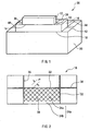
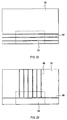
- FIG. 1 shows a construction of a substantial part of the laser diode assembly
- Fig. 2 shows a construction of grooves of a submount
- Fig. 3 shows a construction of grooves of a heatsink, respectively.
- a laser diode assembly 30 of this embodiment comprises a laser diode device 12, a submount 16 jointed to a substrate side of the laser diode device 12 with a first solder layer 14 in between, and a heatsink 20 jointed to a rear face side of the submount 16 with a second solder layer 18 in between as a substantial part similar to a conventional laser assembly 10.
- the submount 16 comprises a groove 32 (hereinafter referred to as submount groove) and an extension groove 36.
- the submount groove 32 is formed around a joint area 34 along border of the joint area 34 jointed with the laser diode device 12.
- the extension groove 36 is a groove extended from the submount groove 32 to edges of the submount 16.
- the submount groove 32 is formed around the joint area 34 along border of the joint area 34 of the submount 16, which is on both side wall sides and a rear end face side opposite of an emitting end face of the laser diode device 12.
- submount thin grooves 38 whose groove width is smaller and whose groove depth is shallower than of the submount groove 32 are formed so that the submount thin grooves 38 are spaced from each other and at least one ends of the submount thin grooves 38 contact with the submount groove 32.
- the submount thin grooves 38 are formed on the joint area 34 of the submount 16 in the shape of lattice and in the direction diagonally to the submount groove 32.
- the submount groove 32 and the submount thin grooves 38 are not provided on the emitting end face side of the laser diode device 12. That is, the submount groove 32 and the submount thin grooves 38 are closed on the emitting end face side of the laser diode device 12.
- the joint area 34 is composed of a joint area 34a wherein the submount thin grooves 38 are arranged and a joint area 34b which is on the continuous same plane as areas other than the joint area 34, wherein the submount thin grooves 38 are not arranged.
- the heatsink 20 also comprises a groove 42 (hereinafter referred to as heatsink groove) formed around a joint area 40 along border of the joint area 40 of the heatsink 20 wherein the submount 16 and the heatsink 20 are jointed and an extension groove 44 extended from the heatsink groove 42 to edges of the heatsink 20.
- heatsink groove a groove 42 (hereinafter referred to as heatsink groove) formed around a joint area 40 along border of the joint area 40 of the heatsink 20 wherein the submount 16 and the heatsink 20 are jointed and an extension groove 44 extended from the heatsink groove 42 to edges of the heatsink 20.
- the heatsink groove 42 is formed around the joint area 40 along border of the joint area 40 of the heatsink 20, which is on the both side wall sides and the rear end face side opposite of the emitting end face of the laser diode device 12.
- a depth and a width of the submount groove 32, the heatsink groove 42, and the extension grooves 36 and 44 are, for example, from 1 ⁇ m to 1 mm.
- a depth and a width of the submount thin groove 38 is approximately from 1 ⁇ m to several hundred ⁇ m.
- solder might excessively flow, or heat release effect of the submount 16 might be lowered.
- the depth and the width of the submount thin groove 38 are too small, providing the thin grooves becomes ineffective.
- a distance P between the respective submount thin grooves 38 is approximately from 1 ⁇ m to 1-2 mm. It is not preferable that the distance P between the submount thin grooves 38 is less than 1 ⁇ m, since irregularity is too fine and a surface of the joint area 34 becomes a state similar to surface roughness. Further, since an area of the joint area 34 is not so large, providing the submount thin grooves 38 becomes ineffective when the distance P is 2 mm or more.
- the submount 16 when solder joint between the laser diode device 12 and the submount 16 is performed, excessive solder flows into the submount groove 32 through the submount thin grooves 38, the submount groove 32 functions as a solder pool for the excessive solder, and the excessive solder is drained outside through the extension groove 36. Therefore, when the laser diode device 12 and the submount 16 are jointed, bulb-shaped excessive solder never remains around the joint area 34 of the submount 16.
- the submount groove 32 and the submount thin grooves 38 are not provided on the emitting end face side of the laser diode device 12. Therefore, excessive solder never flows onto the emitting end face side of the laser diode device 12.
- the heatsink 20 is provided with the heatsink groove 42 and the extension groove 44. Therefore, when solder joint between the submount 16 and the heatsink 20 is performed, excessive solder flows into the heatsink groove 42, the heatsink groove 42 functions as a solder pool for the excessive solder, and the excessive solder is drained outside through the extension groove 44.
- the submount groove 32 it is not necessary to provide the submount groove 32 over a whole length of border of the joint area 34 depending on sizes or shapes of the joint area 34 of the submount 16. It is possible to partly provide the submount groove 32, for example, only at border on the both side wall sides of the laser diode device 12, or only at border on the rear end face side of the laser diode device 12. In such a case, the extension groove 36 contacts with the partly provided submount groove 32.
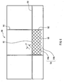
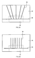
- Fig. 4 shows a construction of submount grooves according to a modification of the laser diode assembly of the first embodiment.
- the submount thin grooves 38 are formed on the joint area 34 of the submount 16 in the shape of lattice and in the direction diagonally to the submount groove 32.
- submount thin grooves 46 are formed on the joint area 34 so that the submount thin grooves 46 are parallel to border of the joint area 34 on the rear end face side of the laser diode device 12.
- thin grooves having a construction similar to of the submount thin grooves can be provided on the joint area 40 of the heatsink 20. It becomes thereby possible that excessive solder further easily flows into the heatsink groove 42 through the thin grooves when solder joint between the submount 16 and the heatsink 20 is performed.
- Fig. 5 shows a construction of a substantial part of a laser diode assembly 50
- Fig. 6 shows a construction of heatsink grooves, respectively.
- the laser diode assembly 50 has the same construction as the conventional laser assembly 10 except that the laser diode device 12 is directly jointed to the heatsink 20 without the foregoing submount 16 in between.
- the heatsink 20 comprises a groove 52 (hereinafter referred to as heatsink groove) and an extension groove 56.
- the heatsink groove 52 is formed around a joint area 54 along border of the joint area 54 jointed with the laser diode device 12.
- the extension groove 56 is extended from the heatsink groove 52 to edges of the heatsink 20.
- the heatsink groove 52 is formed around the joint area 54 along border of the joint area 54 of the heatsink 20 on the both side wall sides and the rear end face side opposite of the emitting end face of the laser diode device 12.
- thin grooves 58 (hereinafter referred to as heatsink thin grooves) whose groove width is smaller and whose groove depth is shallower than of the heatsink groove 52 are formed on the joint area 54 of the heatsink 20 in the shape of lattice and in the direction diagonally to the heatsink groove 52 so that the heatsink thin grooves are spaced from each other and at least one ends of the heatsink thin grooves contact with the heatsink groove 52.
- the heatsink groove 52 and the heatsink thin grooves 58 are not provided on the emitting end face side of the laser diode device 12. That is, the heatsink groove 52 and the heatsink thin grooves 58 are closed on the emitting end face side of the laser diode device 12.
- the joint area 54 is composed of a joint area 54a wherein the heatsink thin grooves 58 are arranged and a joint area 54b which is on the continuous same plane as areas other than the joint area 54, wherein the heatsink thin grooves 58 are not arranged.
- a depth and a width of the heatsink groove 52 and the extension grooves 56 are from 1 ⁇ m to 1 mm.
- a depth and a width of the heatsink thin groove 58 is approximately from 1 ⁇ m to several hundred ⁇ m, considering excessive flow of solder and heat release.
- a distance P between the respective heatsink thin grooves 58 is approximately from 1 ⁇ m to 1-2 mm. It is not preferable that the distance P between the heatsink thin grooves 58 is less than 1 ⁇ m, since a surface of the joint area 54 becomes a state similar to surface roughness. Further, since an area of the joint area 54 is not so large, providing the heatsink thin grooves 58 becomes ineffective when the distance P is 2 mm or more.
- the heatsink groove 52 when solder joint between the laser diode device 12 and the heatsink 20 is performed, excessive solder flows into the heatsink groove 52 through the heatsink thin grooves 58, the heatsink groove 52 functions as a solder pool for the excessive solder, and the excessive solder is drained outside through the extension groove 56.
- the extension groove 56 also has a function as a solder pool for the excessive solder.
- bulb-shaped excessive solder never remains around the joint area 54 of the heatsink 20 when joint between the laser diode device 12 and the heatsink, 20 is performed.
- the joint area of the laser diode device 12 is small, it is possible to provide only the heatsink groove 52. It is not indispensable to provide the submount thin grooves 58.
- the heatsink groove 52 and the heatsink thin grooves 58 are not provided on the emitting end face side of the laser diode device 12. Therefore, excessive solder never flows to the emitting end face side of the laser diode device 12.
- the heatsink groove 52 it is not necessary to provide the heatsink groove 52 over a whole length of border of the joint area 54 depending on sizes or shapes of the joint area 54 of the heatsink 20. It is possible to partly provide the heatsink groove 52, for example, only at border on the both side wall sides of the laser diode device 12, or only at border on the rear end face side of the laser diode device 12. In such a case, the extension groove 56 contacts with the partly provided heatsink groove 52.
- This embodiment relates to a laser diode assembly according to a third example.
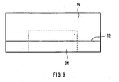
- Fig. 9 shows a construction of a submount groove thereof.
- the laser diode assembly of this embodiment has the same construction as of the laser diode assembly 30 of the first embodiment except that the construction of the submount groove is different.
- the submount 16 comprises one submount transverse groove 62.
- the submount transverse groove 62 crosses the central part of the joint area 34 jointed with the laser diode device 12 (refer to Fig. 1 ) in the direction parallel to the emitting end face of the laser diode device 12 to edges of the submount 16.
- a size of the submount transverse groove 62 is the same as of the submount groove 32 of the first embodiment.
- the submount transverse groove 62 can be plural. Further, it is not indispensable that the submount transverse groove 62 crosses the central part of the joint area 34 of the submount 16.
- the submount transverse groove 62 can cross location of the joint area 34, which is close to the emitting end face.
- bulb-shaped excessive solder never remains around the joint area 34 of the submount 16 when joint between the laser diode device 12 and the submount 16 is performed.
- Fig. 10 shows a construction of a heatsink groove thereof.
- the laser diode assembly of this embodiment is the same as the laser diode assembly 50 of the second embodiment except that the construction of the heatsink groove is different.
- the heatsink 20 comprises a heatsink transverse groove 64.
- the heatsink transverse groove 64 crosses the central part of the joint area 54 jointed with the laser diode device 12 (refer to Fig. 5 ) in the direction parallel to the emitting end face of the laser diode device 12 to edges of the heatsink 20.
- a size of the heatsink transverse groove 64 is the same as of the second heatsink groove 52 of the third embodiment.
- the heatsink transverse groove 62 can be plural. Further, it is not indispensable that the heatsink transverse groove 64 crosses the central part of the joint area 54 of the heatsink 20.
- the heatsink transverse groove 64 can cross location of the joint area 54, which is close to the emitting end face.
- bulb-shaped excessive solder never remains around the joint area 54 of the heatsink 20 when joint between the laser diode device 12 and the heatsink 20 is performed.
- This embodiment relates to a laser diode assembly according to a fifth example.
- Fig. 11 shows a construction of submount grooves thereof.
- the laser diode assembly of this embodiment is the same as the laser diode assembly 30 of the first embodiment except that the construction of the submount grooves is different.
- the submount 16 does not comprise the foregoing submount groove 32 and extension groove 36, but comprises several thin grooves in the joint area 34 jointed with the laser diode device 12 (refer to Fig. 1 ). In this embodiment, only the same thin grooves as the submount thin grooves 38 of the first embodiment are provided.
- the submount 16 comprises the submount thin grooves 38
- excessive solder flows into the submount thin grooves 38
- the submount thin grooves 38 function as a solder pool for the excessive solder when solder joint between the laser diode device 12 and the submount 16 is performed.
- This embodiment relates to a laser diode assembly according to the fifth example.
- Fig. 12 shows a construction of heatsink grooves thereof.
- the laser diode assembly of this embodiment is the same as the laser diode assembly 50 of the second embodiment except that the construction of the heatsink grooves is different.
- the heatsink 20 does not comprise the second heatsink groove 52 and the extension groove 56, but comprises several thin grooves in the joint area 54 jointed with the laser diode device 12 (refer to Fig. 1 ). In this embodiment, only the same thin grooves as the heatsink thin grooves 58 of the second embodiment are provided.
- solder can be stably set while good flatness of the joint area 34 of the submount 16 and the joint area 54 of the heatsink 20 is maintained. Therefore, air entrance between solder and the joint area, or deterioration of contact characteristics between the joint area and solder can be prevented.
- This embodiment relates to a laser diode assembly according to a seventh example.
- Fig. 14 shows a construction of a submount transverse groove thereof.
- the laser diode assembly of this embodiment has the same construction as of the laser diode assembly 30 of the first embodiment except that the groove construction of the submount 16 is different.
- the submount 16 comprises one submount transverse groove 65.
- the submount transverse groove 65 crosses the central part of the joint area 34 jointed with the laser diode device 12 (refer to Fig. 1 ), and extends in the direction parallel to the emitting end face of the laser diode device 12.
- the submount transverse groove 65 is closed at its both ends. As long as excessive solder melt can be pooled, it is not necessary to extend the submount transverse groove 65 to the edges of the submount 16 as the submount transverse groove 62 of the third embodiment.
- a shape of the submount transverse groove 65 is flexible.
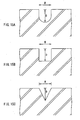
- the submount transverse groove 65 can be a U groove as shown in Fig. 15A .
- a cross section of the submount transverse groove 65 can be rectangle
- a cross section of the submount transverse groove 65 can be triangle.
- each width W and depth D shown in Figs. 15A to 15C is from 1 ⁇ m to 1 mm, and preferably from several dozen ⁇ m to 300 ⁇ m.
- the submount transverse groove 65 is the U groove whose width W and depth D are 150 ⁇ m, respectively.
- solder joint between the laser diode device 12 and the submount 16 when solder joint between the laser diode device 12 and the submount 16 is performed, excessive solder drains into the submount transverse groove 65 and flows inside the submount transverse groove 65 due to capillary thereof, and the submount transverse groove 65 functions as a solder pool for the excessive solder.
- This embodiment relates to a laser diode assembly according to the seventh example.
- Fig. 16 shows a construction of submount transverse grooves thereof.
- the laser diode assembly of this embodiment has the same construction as of the laser diode assembly 30 of the first embodiment except that the groove construction of the submount 16 is different.
- the submount 16 has several (three in this embodiment) submount transverse grooves 66.
- the submount transverse grooves 66 cross the central part of the joint area 34 jointed with the laser diode device 12 (refer to Fig. 1 ), and cross from one edge to the other facing edge of the submount 16 in the direction parallel to the emitting end face of the laser diode device 12.
- An arrangement pitch of the submount transverse grooves 66 is about 1 mm.
- a shape and a size of the submount transverse groove 66 are the same as of the submount transverse groove 65 of the seventh embodiment.
- the pitch varies depending on solder amounts. When the pitch is small, it becomes difficult to maintain flatness in the process.
- the pitch is basically approximately from several hundred ⁇ m to 2 mm.
- the submount transverse grooves 66 function as a solder pool for the excessive solder, and the excessive solder is drained outside.
- Fig. 17 shows a construction of a submount transverse groove thereof.
- the laser diode assembly of this embodiment has the same construction as of the laser diode assembly 30 of the first embodiment except that the groove construction of the submount 16 is different.
- the submount 16 has one submount transverse groove 68.
- the submount transverse groove 68 crosses the central part of the joint area 34 jointed with the laser diode device 12 (refer to Fig. 1 ), and extends from one edge to the other facing edge of the submount 16 in the direction parallel to the emitting end face of the laser diode device 12.
- the submount 16 has several submount branch grooves 70.
- One ends of the submount branch grooves 70 contact with the submount transverse groove 68, and the other ends of the submount branch grooves 70 extend to the edge opposite of the emitting end face side of the laser diode device 12 in the direction perpendicular to the submount transverse groove 68.
- An arrangement pitch of the submount branch grooves 70 is about 1 mm.
- a shape and a size of the submount transverse groove 68 and the submount branch groove 70 are the same as of the submount transverse groove 65 of the seventh embodiment.
- the submount branch grooves 70 are provided in addition to the submount transverse groove 68. Therefore, when solder joint between the laser diode device 12 and the submount 16 is performed, excessive solder flows from the submount transverse groove 68 into the submount branch grooves 70, the excessive solder flows in the submount transverse groove 68 and the submount branch grooves 70 due to capillary phenomenon in the submount transverse groove 68 and the submount branch grooves 70, the submount transverse groove 68 and the submount branch grooves 70 function as a solder pool for the excessive solder, and the excessive solder is drained outside through the submount branch grooves 70.
- the submount branch grooves 70 extend in the direction perpendicular to the submount transverse groove 68.
- the extending direction is in the direction perpendicular to the submount transverse groove 68.
- submount branch grooves 72 can extend to the edge opposite of the emitting end face side in the fan-like shape.
- the submount transverse groove 68 extends from one submount face to the other facing submount face.
- both ends of the submount transverse groove 74 can be closed.
- only one end of the submount transverse groove can be closed.
- one ends of the submount branch grooves 70 extend to the edge opposite of the emitting end face side of the laser diode device in the direction perpendicular to the transverse groove 68.
- the submount branch grooves have enough groove capacities as a solder pool for the excessive solder, as shown in Fig. 18 , the other ends can be closed.
- This embodiment relates to a laser diode assembly according to the seventh example.
- Fig. 20 shows a construction of submount transverse grooves thereof.
- the laser diode assembly of this embodiment has the same construction as of the laser diode assembly 30 of the first embodiment except that the groove construction of the submount 16 is different.
- the submount 16 has several first submount cross grooves 78 and second submount cross grooves 80.
- the first submount cross grooves 78 cross the joint area 34 jointed with the laser diode device 12 (refer to Fig. 1 ) at a crossing angle ⁇ 1 of 40° in relation to an edge of the submount 16 on the emitting end face side of the laser diode device 12.
- the second submount cross grooves 80 cross the joint area 34 at a crossing angle ⁇ 2 of 140°.
- the crossing angle ⁇ 2 its clockwise crossing angle is 40°.
- An arrangement pitch of the first submount cross grooves 78 and the second submount cross grooves 80 is about 1 mm.
- a shape and a size thereof are the same as of the submount transverse groove 65 of the seventh embodiment.
- the first submount cross grooves 78 and the second submount cross grooves 80 are provided. Therefore, when solder joint between the laser diode device 12 and the submount 16 is performed, excessive solder flows into these grooves, the excessive solder flows in these grooves due to capillary phenomenon in these grooves, these grooves function as a solder pool for the excessive solder, and the excessive solder is drained outside.
- the first submount cross grooves 78 and the second submount cross grooves 80 extend to the submount face on the emitting end face side of the laser diode device 12.
- the crossing angles ⁇ 1 and ⁇ 2 are respectively in the angle range specified in the invention. Therefore, solder melt never flows to the submount face on the emitting end face side.
- crossing angles ⁇ 1 and ⁇ 2 are flexible as long as they are 45° or less in relation to the submount face on the emitting end face side.
- Fig. 21 shows a construction of a heatsink groove thereof.
- the laser diode assembly of this embodiment has the same construction as of the laser diode assembly 50 of the second embodiment except that the groove construction of the heatsink 20 is different.
- the heatsink 20 has one heatsink transverse groove 82.
- the heatsink transverse groove 82 crosses the central part of the joint area 54 jointed with the laser diode device 12 (refer to Fig. 1 ), and extends in the direction parallel to the emitting end face of the laser diode device 12.
- this heatsink transverse groove 82 is closed at its both ends. As long as excessive solder melt can be pooled, it is not necessary to extend the heatsink transverse groove to the edges of the heatsink 20 as the heatsink transverse groove 64 of the fourth embodiment.
- Fig. 22 shows a construction of heatsink transverse grooves thereof.
- the laser diode assembly of this embodiment has the same construction as of the laser diode assembly 50 of the second embodiment except that the groove construction of the heatsink 20 is different.
- the heatsink 20 has several (three in this embodiment) heatsink transverse grooves 84.
- the heatsink transverse grooves 84 cross the central part of the joint area 54 jointed with the laser diode device 12 (refer to Fig. 1 ) from one edge to the other facing edge of the heatsink 20 in the direction parallel to the emitting end face of the laser diode device 12.
- An arrangement pitch of the heatsink transverse grooves 84 is about 1 mm.
- a shape and a size of the heatsink transverse groove 84 are the same as of the submount transverse groove 65 of the seventh embodiment.
- Fig. 23 shows a construction of a heatsink transverse groove thereof.
- the laser diode assembly of this embodiment has the same construction as of the laser diode assembly 50 of the second embodiment except that the groove construction of the heatsink 20 is different.
- the heatsink 20 has one heatsink transverse groove 86.
- the heatsink transverse groove 86 crosses the central part of the joint area 54 jointed with the laser diode device 12 (refer to Fig. 1 ), and extends from one edge to the other facing edge of the heatsink 20 in the direction parallel to the emitting end face of the laser diode device 12.
- the heatsink 20 comprises several heatsink branch grooves 88.
- One ends of the heatsink branch grooves 88 contact with the heatsink transverse groove 86, and the other ends of the heatsink branch grooves 88 extend to the edge opposite of the emitting end face side of the laser diode device in the direction perpendicular to the heatsink transverse groove 86.
- An arrangement pitch of the heatsink branch grooves 88 is about 1 mm.
- a shape and a size of the heatsink transverse groove 86 and the heatsink branch groove 88 is the same as of the submount transverse groove 65 of the seventh embodiment.
- the heatsink branch grooves 88 extend in the direction perpendicular to the heatsink transverse groove 86.
- it is not indispensable that the extending direction is in the direction perpendicular to the heatsink transverse groove 86.
- heatsink branch grooves 90 can extend to the edge opposite of the emitting end face side in the fan-like shape.
- the heatsink transverse groove 86 extends from one heatsink face to the other facing heatsink face.
- both ends of a heatsink transverse groove 92 can be closed.
- only one end of the heatsink transverse groove can be closed.
- other ends of the heatsink branch grooves 88 extend to the edge opposite of the emitting end face side of the laser diode device in the direction perpendicular to the heatsink transverse groove 86.
- branch grooves have enough groove capacities as a solder pool for the excessive solder, as shown in Fig 25 , the other ends of heatsink branch grooves 94 can be closed.
- Fig. 26 shows a construction of heatsink transverse grooves thereof.
- the laser diode assembly of this embodiment is the same as the laser diode assembly 50 of the second embodiment except that the groove construction of the heatsink 20 is different.
- the heatsink 20 has several first heatsink cross grooves' 96 and several second heatsink cross grooves 98.
- the first heatsink cross grooves 96 cross the joint area 54 jointed with the laser diode device 12 (refer to Fig. 1 ) at a crossing angle ⁇ 1 of 40° in relation to an edge of the heatsink 20 on the emitting end face side of the laser diode device 12.
- the second heatsink cross grooves 98 cross the joint area 54 at a crossing angle ⁇ 2 of 140°.
- An arrangement pitch of the first heatsink cross grooves 96 and the second heatsink cross grooves 98 is about 1 mm.
- a shape and a size thereof are the same as of the submount transverse groove 65 of the seventh embodiment.
- the first heatsink cross grooves 96 and the second heatsink cross grooves 98 extend to the heatsink face on the emitting end face side of the laser diode device 12.
- the crossing angles ⁇ 1 and ⁇ 2 are respectively in the angle range specified in the invention. Therefore, solder melt never flows to the heatsink face on the emitting end face side.
- crossing angles ⁇ 1 and ⁇ 2 are flexible as long as they are 45° or less in relation to the heatsink face on the emitting end face side.
- This embodiment relates to a method of manufacturing a laser diode assembly according to a ninth example. This embodiment is applied to manufacturing the laser diode assembly of the seventh embodiment.
- the submount 16 which holds the laser diode device 12 on the joint area 34 of the submount 16 is forwarded in a reflow oven, and solder on the joint area 34 of the submount 16 is melted.
- the submount 16 on which the laser diode 12 is fixed is taken out of the reflow oven.
- the heatsink 20 which holds the submount 16 on the joint area 54 of the heatsink 20 is forwarded in the reflow oven, and solder on the joint area 54 of the heatsink 20 is melted. Excessive solder out of the melted solder is drained out between the heatsink 20 and the submount 16, flown and pooled in the heatsink transverse groove due to capillary phenomenon arising in the heatsink transverse groove which crosses the joint area 54 of the heatsink 20.
- the submount 16 is jointed to the heatsink 20.
- joint between the laser diode device 12 and the submount 16 and joint between the submount 16 and the heatsink 20 can be concurrently performed in the reflow oven.
- a method of manufacturing the laser diode assembly according to the tenth example can be performed in a manner similar to in this embodiment basically.
- the submount groove is provided; and in the second invention, when solder joint between the laser diode device and the heatsink is performed, the second heatsink groove is provided. Excessive solder is thereby drained out into the submount groove or the second heatsink groove, the submount groove or the second heatsink groove functions as a solder pool for the excessive solder, and the excessive solder is drained outside. Therefore, bulb-shaped excessive solder never remains around the joint area between the laser diode device and the submount, and the joint area between the laser diode device and the heatsink.
- solder is stably set while good flatness of the joint area is maintained. Therefore, air entrance between solder and the joint area, or deterioration of contact characteristics between the joint area and solder can be prevented.
- the submount transverse groove is provided.
- the heatsink transverse groove is provided. Excessive solder is thereby drained out into the submount transverse groove or the heatsink transverse groove, the submount transverse groove or the heatsink transverse groove functions as a solder pool for the excessive solder, and the excessive solder is drained outside. Therefore, bulb-shaped excessive solder never remains around the joint area between the laser diode device and the submount and the joint area between the laser diode device and the heatsink.
- solder is stably set while good flatness of the joint area is maintained. Therefore, air entrance between solder and the joint area, or deterioration of contact characteristics between the joint area and solder can be prevented.
- the thin grooves are provided on the joint area of the submount.
- the thin grooves are provided on the joint area of the heatsink. Excessive solder is thereby drained out into the thin grooves, and the thin grooves function as a solder pool for the excessive solder. Therefore, bulb-shaped excessive solder never remains around the joint area between the laser diode device and the submount, and the joint area between the laser diode device and the heatsink.
- solder is stably set while good flatness of the joint area is maintained. Therefore, air entrance between solder and the joint area, or deterioration of contact characteristics between the joint area and solder can be prevented.
- the various modes of the submount transverse groove are provided.
- the various modes of the heatsink transverse groove are provided. Excessive solder is thereby drained out into the submount transverse groove or the heatsink transverse groove, the submount transverse groove or the heatsink transverse groove functions as a solder pool for the excessive solder, and the excessive solder is drained outside due to capillary phenomenon in the submount transverse groove or the heatsink transverse groove.
- bulb-shaped excessive solder never remains around the joint area between the laser diode device and the submount, and the joint area between the laser diode device and the heatsink.
Description
- The present invention relates to a laser diode assembly having a structure wherein a laser diode device is jointed to a heatsink with a submount in between or directly.
- More specifically, the invention relates to a laser diode assembly comprising a construction wherein in assembly, solder overflow from a solder joint face between a laser diode device and a submount or a heatsink is inhibited, and overflowing solder does not form bulb-shaped solder residue on the laser diode device, the submount, or the heatsink.
- In a laser diode device, when electrical energy is converted to optical energy, energy loss is generated, and such energy loss is converted to heat energy. This heat energy raises temperature of the laser diode device, and has an unfavorable effect on laser characteristics.
- In order to immediately diffuse such heat energy generated in the laser diode device, and reinforce mechanical strength of the laser diode device, generally, a so-called laser diode assembly, wherein a substrate side of a laser diode device is jointed to a heatsink directly or with a submount in between through a solder layer is manufactured as a produce.
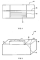
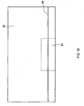
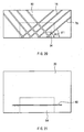
- Specifically, as shown in
Fig. 7 , in a conventionallaser diode assembly 10, alaser diode device 12 is jointed to asubmount 16 through afirst solder layer 14, and thesubmount 16 is jointed to aheatsink 20 through asecond solder layer 18. Thelaser diode device 12 comprises a lamination structure including a light-emitting layer on a semiconductor substrate. There is a structure wherein thelaser diode 12 is directly jointed to theheatsink 20 without thesubmount 16. - The
heatsink 20 is provided with anelectrode pad 24 with an insulating plate 22 in between. Theelectrode pad 24 and an electrode of thelaser diode device 12 are connected (wire bonded) through awire 26. That is, thelaser diode device 12 is connected to outer equipment through theelectrode pad 24. - The
laser diode device 12 is, for example, a GaAs edge-emitting type laser diode device formed on a GaAs substrate. InFig. 7 , an end face opposite of theelectrode pad 24 side is an emitting end face. Number of thelaser diode device 12 can be one as shown inFig. 7 or plural. Some of thelaser diode device 12 are arranged in the shape of an array. - The
submount 16 is a part to reinforce mechanical strength of thelaser diode device 12 and is a metal plate made of, for example, silicon carbide (SiC) or an alloy of copper (Cu) and tungsten (W). Theheatsink 20 is often made of a copper plate. - The
first solder layer 14 to joint thelaser diode device 12 and thesubmount 16 is, for example, a gold-tin (Au/Sn) solder layer. Thesecond solder layer 18 to joint thesubmount 16 and theheatsink 20 is, for example, an indium (In) solder layer. - When such a
laser diode assembly 10 is fabricated, first, thesubmount 16 which lays thelaser diode device 12 on a gold-tin solder plating layer formed on a joint face of thesubmount 16 is forwarded into a reflow oven, and heated to a melting temperature of the gold-tin solder or higher, for example, 300°C to melt the gold-tin solder plating layer. - Next, the
submount 16 placing thelaser diode device 12 is taken out from the reflow oven, and cooled. The melted gold-tin solder plating layer is thereby solidified to become thefirst solder layer 14, and thesubmount 16 and thelaser diode device 12 are jointed. - Subsequently, indium metal vapor is deposited on a joint face of the
heatsink 20 to obtain an indium deposition layer. Thesubmount 16 to which thelaser diode device 12 is jointed is laid on the indium deposition layer. Then, the resultant is forwarded into the reflow oven, heated to 156°C or higher which is a melting temperature of the indium solder, for example, 180°C to melt the indium deposition layer. Next, theheatsink 20 placing thesubmount 16 is taken out from the reflow oven and cooled. The melted indium deposition layer is thereby solidified to become thesecond solder layer 18, and theheatsink 20 and thesubmount 16 are jointed. - In the conventional
laser diode assembly 10, there is an example wherein thesecond solder layer 18 is made of lead-tin solder instead of indium, and an example wherein thefirst solder layer 14 is made of lead-tin solder instead of gold-tin solder. - In Japanese Unexamined Patent Application Publication No.
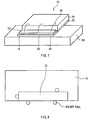
H06-350202 laser diode assembly 10 is disclosed. Another assembly is known fromJP 401127275 U - When the laser diode device is jointed on the submount, or the submount is jointed on the heatsink, even if the same amount of solder is provided every time, a part of excessive solder overflows from the joint face, since surface state of the joint faces of the laser diode device, the submount, or the heatsink is subtly changed.
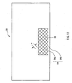
- As shown in
Fig. 8 , the overflowing solder is swollen in the shape of a bulb, and remains at edges of the joint area, particularly at edges of the laser diode device. This phenomenon that solder is swollen in the shape of a bulb is significant particularly when flux is not used. - The solder residue may become an obstacle in subsequent mounting of the laser diode assembly, or have an adverse effect on laser characteristics. In particular, if the bulb-shaped solder residue is formed on the emitting end face side of the laser diode device when the laser diode device is jointed on the submount or the heatsink, it is not preferable for the laser characteristics.
- In view of the foregoing, it is an object of the invention to provide a laser diode assembly which can, in assembly, inhibit solder overflow from a solder joint face, and prevent the overflowing solder from forming bulb-shaped solder residue on a laser diode device, a submount, or a heatsink.
- The inventors have noted the following in the process of the research to solve the problems. That is, the submount and the heatsink to mount the laser diode device are greatly premised on that their joint areas have high flatness in order to attain good mounting. However, when solid solder is temporarily fixed before the laser diode device is mounted on the submount or the heatsink, excessive fine flatness of the joint area works adversely. That is, contact becomes hard, peeling is caused, air enters, leading to joint failure.
- Meanwhile, lowering flatness of the submount or the heatsink has an unfavorable effect on mounting precision itself.
- Therefore, in order to attain good joint, the inventor has devised providing grooves, which maintain flatness of the joint area of the submount or the heatsink in the perfect state as long as possible, and which makes excessive solder flow around the joint area in order to process the excessive solder. The inventor has confirmed the validity thereof through experiments, and realized the following assemblies.
- The invention as defined in the claims comprises aspects of the first and second examples.
- Specifically, the first example is a laser diode assembly comprising: a laser diode device; a submount jointed on a substrate side of the laser diode device with a first solder layer in between; and a heatsink jointed on a rear face side of the submount with a second solder layer in between, wherein the submount has a groove (hereinafter referred to submount groove) at least at a part of a periphery of a joint area along border of the joint area jointed with the laser diode device.
- In this laser diode assembly, when solder joint between the laser diode device and the submount is performed, excessive solder flows into the submount groove. That is, the submount groove functions as a solder pool for the excessive solder, and further works to drain the excessive solder outside. Therefore, bulb-shaped excessive solder never remains around the joint area between the laser diode device and the submount.
- It is not indispensable to provide the submount groove at a whole length of the periphery of the joint area. When the submount groove is provided only at a part of the periphery, the foregoing effect can be obtained on some level.
- Further, in this laser diode assembly, the heatsink can have a groove (hereinafter referred to as heatsink groove) around its joint area along border of a joint area jointed with the submount.
- Therefore, when solder joint between the submount and the heatsink is performed, excessive solder flows into the heatsink groove. That is, the heatsink groove functions as a solder pool for the excessive solder, and further works to drain the excessive solder outside. Consequently, bulb-shaped excessive solder never remains also around the joint area between the submount and the heatsink.
- Next, the second example is a laser diode assembly comprising: a laser diode device; and a heatsink jointed on a substrate side of the laser diode device with a solder layer in between, wherein the heatsink has a groove (hereinafter referred to as second heatsink groove) at least at a part of a periphery of a joint area along border of the joint area jointed with the laser diode device.
- In this laser diode assembly, the laser diode device is directly jointed to the heatsink. When solder joint between this laser diode device and the heatsink is performed, excessive solder flows into the second heatsink groove as in the foregoing. Therefore, bulb-shaped excessive solder never remains around the joint area between the laser diode device and the heatsink.
- It is not indispensable to provide the second heatsink groove at a whole length of the periphery of the joint area. When the second heatsink groove is provided only at a part of the periphery of the joint area, effect of the invention can be obtained on some level.
- In the first and the second inventions, it is preferable that the submount groove or the heatsink groove is formed along border of the joint area on a rear end face side opposite of an emitting end face of the laser diode device, and border of the joint area on both wall sides of the laser diode device.
- It is not preferable that excessive solder flows onto the emitting end face side of the laser diode device. Therefore, it is preferable not to provide the submount groove and the heatsink groove on the emitting end face side.
- In the first example, it is more preferable that several thin grooves whose width is smaller and depth is shallower than that of the submount groove are formed on the joint area of the submount so that the thin grooves are spaced from each other and at least one ends of the thin grooves contact with the submount groove.
- Similarly, in the second example, several heatsink thin grooves whose width is smaller and depth is shallower than that of the second heatsink groove are formed on the joint area of the heatsink so that the heatsink thin grooves are spaced from each other and at least one ends of the heatsink thin grooves contact with the second heatsink groove.
- In the first example, in order to improve joint characteristics between the submount and the heatsink, it is possible to provide thin grooves having a construction similar to that of the submount thin grooves in the joint area of the heatsink.
- By providing the submount thin grooves and the heatsink thin grooves, when jointing the laser diode device, it becomes possible to further facilitate excessive solder flowing from the joint area, and improve contact characteristics between the laser diode device and the submount.
- Further, when solid solder is used, the thin grooves in the joint area facilitate contact temporally fixing of solder. Therefore, remaining air between solder and the submount or the heatsink, which causes joint failure such as floatage never arises.
- Arrangement of the submount thin grooves or the heatsink thin grooves is not limited. However, it is preferable that the thin grooves are provided so that the thin grooves extend in the direction diagonally to the submount groove or the second heatsink groove, or extend in the direction parallel to border of the joint area on the rear end face side of the laser diode device. Flowing of excessive solder onto the emitting end face side of the laser diode device thereby can be inhibited.
- It is more preferable that outlets on the emitting end face side of the laser diode device of the submount groove, the heatsink groove, the second heatsink groove, and the thin grooves are closed. Therefore, flowing of excessive solder onto the emitting end face side of the laser diode device can be inhibited.
- Further, in the first example, an extension groove of the submount groove can extend to ends of the submount. In the second invention, an extension groove of the second heatsink groove can extend to ends of the heatsink. Therefore, excessive solder pooled in the submount groove or the second heatsink groove can easily flow outside through the extension groove.
- A depth and a width of the submount groove, the heatsink groove, the second heatsink groove, and the extension groove are in the range from 1 µm to 1 mm. When the size is less than 1 µm, it is difficult to drain excessive solder. On the contrary, if the size is over 1 mm, effect is not improved, and strength of the submount and the heatsink may be lowered.
- When the submount thin grooves or the heatsink thin grooves are too large, solder may flow too much, or heat release effect of the submount or the heatsink may be lowered. Meanwhile, when the thin grooves are too small, providing the thin grooves becomes ineffective. Considering the foregoing, a depth and a width of the submount thin groove and the heatsink thin groove are approximately from 1 µm to several hundred µm. A distance between respective submount thin grooves or the respective heatsink thin grooves is approximately from 1 µm to 1·2 mm. It is not preferable that the distance between the respective submount thin grooves or the respective heatsink thin grooves is less than 1 µm, since irregularity in the joint area is too fine and a surface of the joint area becomes a state similar to surface roughness. Meanwhile, since an area of the joint area is not so large, providing the submount thin grooves and the heatsink thin grooves becomes ineffective when the distance thereof is equal to or more than 2 mm.
- It is not indispensable that the submount groove or the heatsink groove is provided at border of the joint area. A groove crossing the joint area can provide effect of the invention.
- That is, still other laser diode assembly (hereinafter referred to as the third example) is a laser diode assembly comprising a laser diode device; a submount jointed on a substrate side of the laser diode device with a first solder layer in between; and a heatsink jointed on a rear face side of the submount with a second solder layer in between, wherein the submount has a groove (hereinafter referred to as submount transverse groove) which crosses a joint area jointed with the laser diode device, and reaches edges of the submount.
- Number of the submount transverse groove can be one or plural. Further, it is not necessary that several submount transverse grooves are parallel to each other. It is preferable that the submount transverse groove crosses the joint area of the submount so that the submount transverse groove crosses any of border on the side wall sides and border on the rear end face side of the laser diode device in the joint area of the submount, and does not cross border on the emitting end face side, to prevent solder from flowing onto the emitting end face side of the laser diode device. Further, it is more preferable that the submount transverse groove crosses approximately the center of the joint area of the submount in the direction parallel to the emitting end face of the laser diode device.
- Further, still other laser diode assembly (hereinafter referred to as the fourth example) is a laser diode assembly comprising: a laser diode device; and a heatsink jointed on a substrate side of the laser diode device with a solder layer in between, wherein the heatsink has a groove (hereinafter referred to as heatsink transverse groove) which crosses a joint area jointed with the laser diode device, and reaches edges of the heatsink.
- Number of the heatsink transverse groove can be one or plural. Further, it is not necessary that several heatsink transverse grooves are parallel to each other. It is preferable that the heatsink transverse groove crosses the joint area of the heatsink so that the heatsink transverse groove crosses any of border on the side wall sides and border on the rear end face side of the laser diode device in the joint area of the heatsink, and does not cross border on the emitting end face side, to prevent solder from flowing onto the emitting end face side of the laser diode device. Further, it is more preferable that the heatsink transverse groove crosses approximately the center of the joint area of the heatsink in the direction parallel to the emitting end face of the laser diode device.
- In the third and the fourth examples, by providing the submount transverse groove and the heatsink transverse groove, when solder joint between the laser diode device and the submount is performed, or solder joint between the laser diode device and the heatsink is performed, excessive solder flows into the submount transverse groove and the heatsink transverse groove, the submount transverse groove and the heatsink transverse groove function as a solder pool for the excessive solder, and the excessive solder is drained outside. Therefore, bulb-shaped excessive solder never remains around the joint area between the laser diode device and the submount, or the joint area between the laser diode device and the heatsink.
- Respective sizes of the submount transverse groove and the heatsink transverse groove can be the same as of the submount groove and the second heatsink groove.
- In the first invention, the submount groove is provided, and the submount thin grooves are further provided. In the second invention, the second heatsink groove is provided, and the heatsink thin grooves are further provided. However, when grooves corresponding to the submount thin grooves or the heatsink thin grooves are provided on the joint area of the submount or the heatsink without the submount groove or the second heatsink groove, effect of the invention can be also obtained.
- That is, still other laser diode assembly (hereinafter referred to as the fifth example) is a laser diode assembly comprising: a laser diode device; a submount jointed on as substrate side of the laser diode device with a first solder layer in between; and a heatsink jointed on a rear face side of the submount with a second solder layer in between, wherein the submount has several thin grooves in a joint area jointed with the laser diode device.
- Further, still other laser diode assembly (hereinafter referred to as the sixth example) is a laser diode assembly comprising: a laser diode device; and a heatsink jointed on a substrate side of the laser diode device with a solder layer in between, wherein the heatsink has several thin grooves in a joint area jointed with the laser diode device.
- In the fifth and the sixth examples, respective sizes of the grooves provided in the joint area of the submount and the joint area of the heatsink can be the same as of the submount thin grooves and the heatsink thin grooves. Arrangement of the grooves is flexible. For example, the grooves can be several thin grooves parallel to each other, or thin grooves in the shape of lattice.
- In the first and second invention and third to the sixth examples, the laser diode device can be a laser diode device in the shape of a chip, in the shape of a laser bar, or in the shape of a two dimensional array. Further, solder types are not limited. Solder can be solid type or cream type. Further, materials for the submount and the heatsink are not limited.
- In the process of further researching the method of manufacturing the laser diode assembly, the following was confirmed by experiments.
- First, as shown in
Fig. 13 , in a laser diode assembly mounting a laser diode device whose heat release value during operation is large, when a submount groove or a heatsink groove is provided along border of a joint area of a submount or border of a joint area of a heatsink, due to an air layer pooling in the submount groove or the heatsink groove, heat conductivity from the laser diode device to the submount and heat conductivity from the submount to the heatsink become lowered, and heat release characteristics of the heat release value generated in the laser diode device may be lowered in some cases. - Therefore, in such a laser diode assembly mounting the laser diode device whose heat release value is large, in order to maintain good heat release characteristics of the laser diode device, it is appropriate not to provide the submount groove or the heatsink groove along the joint area of the submount or the joint area of the heatsink in many cases.
- Secondly, fluidity of solder melt in a submount transverse groove or a heatsink transverse groove whose groove diameter is small depends on capillary phenomenon.
- Thirdly, even when a submount transverse groove or a heatsink transverse groove crosses a submount face or a heatsink face on the emitting end face side of the laser diode device at a obtuse crossing angle of, for example, 45° or less, the crossing angle is smaller than in the case that the transverse groove crosses perpendicular to the submount face or the heatsink face. Therefore, it was found that in this case, excessive solder does not flow onto the submount face or the heatsink face on the emitting end face side of the laser diode device.
- Fourthly, in the third and the fourth examples, the submount transverse groove or the heatsink transverse groove extends from edge to edge of the submount or the heatsink. However, as long as the submount transverse groove or the heatsink transverse groove has a groove capacity capable of housing excessive solder, it is not necessary that the submount transverse groove or the heatsink transverse groove extends from edge to edge of the submount or the heatsink.
- Therefore, based on the foregoing knowledge, a laser diode assembly according to the invention (hereinafter referred to as the seventh invention) is a laser diode assembly comprisng a laser diode device; a submount jointed on a substrate side of the laser diode device with a first solder layer in between; and a heatsink jointed on a rear face side of the submount with a second solder layer in between, wherein the submount has a groove (hereinafter referred to as submount transverse groove) which extends in a joint area jointed with the laser diode device without crossing a submount face on the emitting end face side of the laser diode device, or a groove (hereinafter referred to as submount cross groove) which crosses the submount face on the emitting end face side of the laser diode device at a crossing angle of 45° or less, and extends in the joint area of the submount.
- The seventh example is a laser diode assembly wherein the laser diode device is jointed to the heatsink with the submount in between. By providing the submount transverse groove, when solder joint between the laser diode device and the submount is performed, excessive solder melt flows into the submount transverse groove, and flows in the submount transverse groove due to capillary phenomenon of the submount transverse groove, the submount transverse groove functions as a solder pool for the excessive solder melt, and the excessive solder melt is drained outside.
- Therefore, bulb-shaped excessive solder never remains around the joint area between the laser diode device and the submount.
- Number of the submount transverse groove and the submount cross groove is not limited, and can be one or plural depending on sizes of the joint area of the laser diode device. Further, it is not necessary that the submount transverse groove and the submount cross groove extend from one submount face to the other submount face. As long as the submount transverse groove and the submount cross groove function as a solder pool for excessive solder melt, their both ends can be closed.
- It is preferable to provide submount branch grooves whose one ends contact with the submount transverse groove, and which extend in the direction crossing the submount transverse grove.
- Excessive solder melt which is pooled in the submount transverse groove or the submount cross groove thereby can be drained into the submount branch grooves, pooled in the submount branch grooves due to capillary phenomenon, or drained out outside.
- Unless excessive solder melt overflows onto the submount surface since the submount branch grooves are short, it is not indispensable that the submount branch grooves extend to the submount face opposite of the emitting end face side of the laser diode device.
- In the seventh example, as the submount, the heatsink can comprises a groove (hereinafter referred to as heatsink transverse groove) which extends in a joint area jointed of the heatsink on which the submount is jointed without crossing a heatsink face on the emitting end face side of the laser diode device, or a groove (hereinafter referred to as heatsink cross groove) which crosses the heatsink face on the emitting end face side of the laser diode device at a crossing angle of 45° or less, and extends in the joint area of the heatsink.
- Further, it is possible to provide heatsink branch grooves whose one ends contact with the heatsink transverse groove, and which extend in the direction crossing the heatsink transverse grove.
- In the foregoing construction of the seventh example, by providing the heatsink transverse groove or the heatsink cross groove, when solder joint between the submount and the heatsink is performed, excessive solder melt is drained into the heatsink transverse groove, the excessive melt flows in the heatsink transverse groove due to capillary phenomenon of the heatsink transverse groove, the heatsink transverse groove functions as a solder pool for the excessive solder melt, and the excessive solder melt is drained outside. Therefore, bulb-shaped excessive solder never remains around the joint area between the submount and the heatsink.
- Number of the heatsink transverse groove and the heatsink cross groove is not limited, and can be one or plural depending on sizes of the joint area of the heatsink. Further, it is not necessary that the heatsink transverse groove and the heatsink cross groove extend from one heatsink face to the other heatsink face. As long as the heatsink transverse groove and the heatsink cross groove function as a solder pool for excessive solder melt, their both ends can be closed.
- A groove diameter of the submount transverse groove, the submount cross groove, the submount branch groove, the heatsink transverse groove, the heatsink cross groove, and the heatsink branch groove is preferably a groove diameter with which capillary phenomenon of solder melt which joints the laser diode device or the submount is generated. In this specification, the capillary phenomenon of solder melt means that fluidity of solder melt is improved by the submount transverse groove and the like with a small groove diameter.
- When a groove diameter is larger than the groove diameter with which the capillary phenomenon of solder melt is generated, a drawback of lowered heat release characteristics becomes more significant than an advantage of drainage of excessive solder melt. Meanwhile, when a groove diameter is too small, fluid resistance of solder melt inside the groove with a small groove diameter becomes larger than improvement of fluidity of solder melt due to the capillary phenomenon, so that fluidity of solder melt is lowered, and occlusion may be caused. Generally, the groove size is from 1 µm to 1 mm, or from several dozen µm to 300 µm.
- A laser diode assembly (hereinafter referred to as the eighth example) is a laser diode assembly comprising: a laser diode device; and a heatsink jointed on a substrate side of the laser diode device with a solder layer in between, wherein the heatsink has a groove (hereinafter referred to as heatsink transverse groove) which extends in a joint area jointed with the laser diode device without crossing a heatsink face on the emitting end face side of the laser diode device, or a groove (hereinafter referred to as heatsink cross groove) which crosses the submount face on the emitting end face side of the laser diode device at a crossing angle of 45° or less, and extends in the joint area of the submount.
- In the eighth example, the laser diode device is directly jointed to the heatsink. By providing the heatsink transverse groove or the heatsink cross groove, when solder joint between the laser diode device and the heatsink is performed, it is possible that excessive solder melt is drained into the heatsink transverse groove, the excessive solder melt flows in the heatsink transverse groove due to capillary phenomenon of the heatsink transverse groove, the heatsink transverse groove functions as a solder pool for the excessive solder melt, and the excessive solder melt is drained outside.
- Therefore, bulb-shaped excessive solder never remains around the joint area between the laser diode device and the heatsink.
- Number of the heatsink transverse groove and the heatsink cross groove is not limited, and can be one or plural depending on sizes of the joint area of the laser diode device. Further, it is not necessary that the heatsink transverse groove and the heatsink cross groove extend from one heatsink face to the other heatsink face. As long as the heatsink transverse groove and the heatsink cross groove can function as a solder pool for excessive solder melt, their both ends can be closed.
- Further, in the eighth example, it is preferable to provide heatsink branch grooves whose one ends contact with the heatsink transverse groove and which extend in the direction crossing the heatsink transverse groove.
- Similarly to of the seventh example, each groove diameter of the heatsink transverse groove, the heatsink cross groove, and the heatsink branch groove is about a size with which capillary phenomenon of solder melt is generated.
- A method of manufacturing a laser diode assembly (hereinafter referred to as the ninth example) is a method of manufacturing a laser diode assembly having a structure in which a laser diode device is jointed to a heatsink with a submount in between, when the laser diode device is jointed to the submount, comprising the steps of: forwarding the submount holding the laser diode device on a joint area of the submount into a reflow oven, and melting solder on the joint area of the submount; and draining excessive solder out of the melted solder between the submount and the laser diode device due to capillary phenomenon generated in a groove crossing the joint area of the submount, and pooling the excessive solder in the groove.
- In the ninth example, excessive solder out of the melted solder flows between the submount and the laser diode device due to capillary phenomenon generated in the groove crossing the joint area of the submount, and is pooled in the groove. Therefore, when solder joint between the laser diode device and the submount is performed, bulb-shaped excessive solder never remains around the joint area between the laser diode device and the submount.
- Further, when the submount is jointed to the heatsink, the ninth invention comprises the steps of: forwarding the heatsink holding the submount on a joint area of the heatsink into a reflow oven, and melting solder on the joint area of the heatsink; and draining excessive solder out of the melted solder between the heatsink and the submount due to capillary phenomenon generated in a groove crossing the joint area of the heatsink, and pooling the excessive solder in the groove.
- In the foregoing construction, excessive solder out of the melted solder flows between the submount and the heatsink due to capillary phenomenon generated in the groove crossing the joint area of the heatsink, and is pooled in the groove. Therefore, when solder joint between the submount and the heatsink is performed, bulb-shaped excessive solder never remains around the joint area between the submount and the heatsink.
- Other method of manufacturing a laser diode assembly (hereinafter referred to as the tenth example) is a method of manufacturing a laser diode assembly having a structure in which a laser diode device is jointed to a heatsink, when the laser diode device is jointed to the heatsink, comprising the steps of: forwarding the heatsink holding the laser diode device on a joint area of the heatsink into a reflow oven, and melting solder on the joint area of the heatsink; and draining excessive solder out of the melted solder between the heatsink and the laser diode device due to capillary phenomenon generated in a groove crossing the joint area of the heatsink, and pooling the excessive solder in the groove.
- In the tenth example, excessive solder out of the melted solder flows between the heatsink and the laser diode device due to capillary phenomenon generated in the groove crossing the joint area of the heatsink, and is pooled in the groove. Therefore, when solder joint between the laser diode device and the heatsink is performed, bulb-shaped excessive solder never remains around the joint area between the laser diode device and the heatsink.
-
-
Fig. 1 is an oblique perspective figure showing a construction of a substantial part of a laser diode assembly according to a first embodiment of the assembly; -
Fig. 2 is a plane view showing a construction of submount grooves; -
Fig. 3 is a plane view showing a construction of heatsink grooves; -
Fig. 4 is a plane view showing a construction of submount grooves of a modification of the first embodiment; -
Fig. 5 is an oblique perspective figure showing a construction of a substantial part of a laser diode assembly according to a second embodiment; -
Fig. 6 is a plane view showing a construction of heatsink grooves; -
Fig. 7 is an oblique perspective figure showing a construction of a conventional laser diode assembly; -
Fig. 8 is a plane view of a submount to explain problems of the conventional laser diode assembly; -
Fig. 9 is a plane view showing a construction of a submount groove of a laser diode assembly according to a third embodiment; -
Fig. 10 is a plane view showing a construction of a heatsink groove of a laser diode assembly according to a fourth embodiment; -
Fig. 11 is a plane view showing a construction of submount grooves of a laser diode assembly according to a fifth embodiment; -
Fig. 12 is a plane view showing a construction of heatsink grooves of a laser diode assembly according to a sixth embodiment; -
Fig. 13 is a cross sectional view to explain failure when a laser diode device and a submount are jointed; -
Fig. 14 is a plane view showing a construction of a submount groove of a laser diode assembly according to a seventh embodiment; -
Figs. 15A to 15C are cross sectional views showing shapes and sizes of respective grooves; -
Fig. 16 is a plane view showing a construction of submount grooves of a laser diode assembly according to an eighth embodiment; -
Fig. 17 is a plane view showing a construction of submount grooves of a laser diode assembly according to a ninth embodiment; -
Fig. 18 is a plane view showing a construction of submount grooves of a laser diode assembly according to a modification of the ninth embodiment; -
Fig. 19 is a plane view showing a construction of submount grooves of a laser diode assembly according to other modification of the ninth embodiment; -
Fig. 20 is a plane view showing a construction of submount grooves of a laser diode assembly according to a tenth embodiment; -
Fig. 21 is a plane view showing a construction of a heatsink groove of a laser diode assembly according to an eleventh embodiment; -
Fig. 22 is a plane view showing a construction of heatsink grooves of a laser diode assembly according to a twelfth embodiment; -
Fig. 23 is a plane view showing a construction of heatsink grooves of a laser diode assembly according to a thirteenth embodiment; -
Fig. 24 is a plane view showing a construction of heatsink grooves of a laser diode assembly according to a modification of the thirteenth embodiment; -
Fig. 25 is a plane view showing a construction of heatsink grooves of a laser diode assembly according to other modification of the thirteenth embodiment; and -
Fig. 26 is a plane view showing a construction of heatsink grooves of a laser diode assembly according to a fourteenth embodiment. - Concrete and detailed descriptions will be hereinafter given of embodiments of the assembly with reference to the attached drawings. In the following embodiments and modifications, the same components as in a conventional construction (
Fig. 7 ) will be described with the same symbols as in the conventional construction. - This embodiment is an example of a laser diode assembly according to a first invention.
Fig. 1 shows a construction of a substantial part of the laser diode assembly,Fig. 2 shows a construction of grooves of a submount, andFig. 3 shows a construction of grooves of a heatsink, respectively. - As shown in
Fig. 1 , alaser diode assembly 30 of this embodiment comprises alaser diode device 12, asubmount 16 jointed to a substrate side of thelaser diode device 12 with afirst solder layer 14 in between, and aheatsink 20 jointed to a rear face side of thesubmount 16 with asecond solder layer 18 in between as a substantial part similar to aconventional laser assembly 10. - In the
laser diode assembly 30, thesubmount 16 comprises a groove 32 (hereinafter referred to as submount groove) and anextension groove 36. Thesubmount groove 32 is formed around ajoint area 34 along border of thejoint area 34 jointed with thelaser diode device 12. Theextension groove 36 is a groove extended from thesubmount groove 32 to edges of thesubmount 16. - The
submount groove 32 is formed around thejoint area 34 along border of thejoint area 34 of thesubmount 16, which is on both side wall sides and a rear end face side opposite of an emitting end face of thelaser diode device 12. - Further, in the
submount 16, many thin grooves 38 (hereinafter referred to as submount thin grooves), whose groove width is smaller and whose groove depth is shallower than of thesubmount groove 32 are formed so that the submountthin grooves 38 are spaced from each other and at least one ends of the submountthin grooves 38 contact with thesubmount groove 32. The submountthin grooves 38 are formed on thejoint area 34 of thesubmount 16 in the shape of lattice and in the direction diagonally to thesubmount groove 32. - In this embodiment, the
submount groove 32 and the submountthin grooves 38 are not provided on the emitting end face side of thelaser diode device 12. That is, thesubmount groove 32 and the submountthin grooves 38 are closed on the emitting end face side of thelaser diode device 12. Thejoint area 34 is composed of ajoint area 34a wherein the submountthin grooves 38 are arranged and ajoint area 34b which is on the continuous same plane as areas other than thejoint area 34, wherein the submountthin grooves 38 are not arranged. - As shown in
Figs. 1 and3 , theheatsink 20 also comprises a groove 42 (hereinafter referred to as heatsink groove) formed around ajoint area 40 along border of thejoint area 40 of theheatsink 20 wherein thesubmount 16 and theheatsink 20 are jointed and anextension groove 44 extended from theheatsink groove 42 to edges of theheatsink 20. - The
heatsink groove 42 is formed around thejoint area 40 along border of thejoint area 40 of theheatsink 20, which is on the both side wall sides and the rear end face side opposite of the emitting end face of thelaser diode device 12. - Though not shown, it is possible to provide thin grooves similar to the submount
thin grooves 38 in thejoint area 40 of theheatsink 20. - A depth and a width of the
submount groove 32, theheatsink groove 42, and theextension grooves - Meanwhile, a depth and a width of the submount
thin groove 38 is approximately from 1 µm to several hundred µm. When the depth and the width of the submountthin groove 38 are too large, solder might excessively flow, or heat release effect of thesubmount 16 might be lowered. On the contrary, when the depth and the width of the submountthin groove 38 are too small, providing the thin grooves becomes ineffective. A distance P between the respective submountthin grooves 38 is approximately from 1 µm to 1-2 mm. It is not preferable that the distance P between the submountthin grooves 38 is less than 1 µm, since irregularity is too fine and a surface of thejoint area 34 becomes a state similar to surface roughness. Further, since an area of thejoint area 34 is not so large, providing the submountthin grooves 38 becomes ineffective when the distance P is 2 mm or more. - In this embodiment, regarding the
submount 16, when solder joint between thelaser diode device 12 and thesubmount 16 is performed, excessive solder flows into thesubmount groove 32 through the submountthin grooves 38, thesubmount groove 32 functions as a solder pool for the excessive solder, and the excessive solder is drained outside through theextension groove 36. Therefore, when thelaser diode device 12 and thesubmount 16 are jointed, bulb-shaped excessive solder never remains around thejoint area 34 of thesubmount 16. - When a joint area of the
laser diode device 12, that is, thejoint area 34 of thesubmount 16 is small, it is possible to provide only thesubmount groove 32. It is not indispensable to provide the submountthin grooves 38. - Further, in this embodiment, the
submount groove 32 and the submountthin grooves 38 are not provided on the emitting end face side of thelaser diode device 12. Therefore, excessive solder never flows onto the emitting end face side of thelaser diode device 12. - Furthermore, the
heatsink 20 is provided with theheatsink groove 42 and theextension groove 44. Therefore, when solder joint between the submount 16 and theheatsink 20 is performed, excessive solder flows into theheatsink groove 42, theheatsink groove 42 functions as a solder pool for the excessive solder, and the excessive solder is drained outside through theextension groove 44. - Therefore, bulb-shaped excessive solder never remains around the
joint area 40 of theheatsink 20. - It is not necessary to provide the
submount groove 32 over a whole length of border of thejoint area 34 depending on sizes or shapes of thejoint area 34 of thesubmount 16. It is possible to partly provide thesubmount groove 32, for example, only at border on the both side wall sides of thelaser diode device 12, or only at border on the rear end face side of thelaser diode device 12. In such a case, theextension groove 36 contacts with the partly providedsubmount groove 32. -
Fig. 4 shows a construction of submount grooves according to a modification of the laser diode assembly of the first embodiment. - In the first embodiment, the submount
thin grooves 38 are formed on thejoint area 34 of thesubmount 16 in the shape of lattice and in the direction diagonally to thesubmount groove 32. In this modification, submountthin grooves 46 are formed on thejoint area 34 so that the submountthin grooves 46 are parallel to border of thejoint area 34 on the rear end face side of thelaser diode device 12. - In this modification, when solder joint between the
laser diode device 12 and thesubmount 16 is performed, effect similar to in the first example can be obtained by providing the submountthin grooves 46. - Further, as other modification, though not shown, thin grooves having a construction similar to of the submount thin grooves can be provided on the
joint area 40 of theheatsink 20. It becomes thereby possible that excessive solder further easily flows into theheatsink groove 42 through the thin grooves when solder joint between the submount 16 and theheatsink 20 is performed. - This embodiment relates to a laser diode assembly according to a second invention.
Fig. 5 shows a construction of a substantial part of alaser diode assembly 50, andFig. 6 shows a construction of heatsink grooves, respectively. - The
laser diode assembly 50 has the same construction as theconventional laser assembly 10 except that thelaser diode device 12 is directly jointed to theheatsink 20 without the foregoingsubmount 16 in between. - In this embodiment, the
heatsink 20 comprises a groove 52 (hereinafter referred to as heatsink groove) and anextension groove 56. Theheatsink groove 52 is formed around ajoint area 54 along border of thejoint area 54 jointed with thelaser diode device 12. Theextension groove 56 is extended from theheatsink groove 52 to edges of theheatsink 20. - The
heatsink groove 52 is formed around thejoint area 54 along border of thejoint area 54 of theheatsink 20 on the both side wall sides and the rear end face side opposite of the emitting end face of thelaser diode device 12. - Further, thin grooves 58 (hereinafter referred to as heatsink thin grooves) whose groove width is smaller and whose groove depth is shallower than of the
heatsink groove 52 are formed on thejoint area 54 of theheatsink 20 in the shape of lattice and in the direction diagonally to theheatsink groove 52 so that the heatsink thin grooves are spaced from each other and at least one ends of the heatsink thin grooves contact with theheatsink groove 52. - Further, in this embodiment, the
heatsink groove 52 and the heatsinkthin grooves 58 are not provided on the emitting end face side of thelaser diode device 12. That is, theheatsink groove 52 and the heatsinkthin grooves 58 are closed on the emitting end face side of thelaser diode device 12. Thejoint area 54 is composed of ajoint area 54a wherein the heatsinkthin grooves 58 are arranged and ajoint area 54b which is on the continuous same plane as areas other than thejoint area 54, wherein the heatsinkthin grooves 58 are not arranged. - A depth and a width of the
heatsink groove 52 and theextension grooves 56 are from 1 µm to 1 mm. - Meanwhile, a depth and a width of the heatsink
thin groove 58 is approximately from 1 µm to several hundred µm, considering excessive flow of solder and heat release. A distance P between the respective heatsinkthin grooves 58 is approximately from 1 µm to 1-2 mm. It is not preferable that the distance P between the heatsinkthin grooves 58 is less than 1 µm, since a surface of thejoint area 54 becomes a state similar to surface roughness. Further, since an area of thejoint area 54 is not so large, providing the heatsinkthin grooves 58 becomes ineffective when the distance P is 2 mm or more. - In this embodiment, when solder joint between the
laser diode device 12 and theheatsink 20 is performed, excessive solder flows into theheatsink groove 52 through the heatsinkthin grooves 58, theheatsink groove 52 functions as a solder pool for the excessive solder, and the excessive solder is drained outside through theextension groove 56. Theextension groove 56 also has a function as a solder pool for the excessive solder. - Therefore, bulb-shaped excessive solder never remains around the
joint area 54 of theheatsink 20 when joint between thelaser diode device 12 and the heatsink, 20 is performed. When the joint area of thelaser diode device 12 is small, it is possible to provide only theheatsink groove 52. It is not indispensable to provide the submountthin grooves 58. - Further, in this embodiment, the
heatsink groove 52 and the heatsinkthin grooves 58 are not provided on the emitting end face side of thelaser diode device 12. Therefore, excessive solder never flows to the emitting end face side of thelaser diode device 12. - It is not necessary to provide the
heatsink groove 52 over a whole length of border of thejoint area 54 depending on sizes or shapes of thejoint area 54 of theheatsink 20. It is possible to partly provide theheatsink groove 52, for example, only at border on the both side wall sides of thelaser diode device 12, or only at border on the rear end face side of thelaser diode device 12. In such a case, theextension groove 56 contacts with the partly providedheatsink groove 52. - This embodiment relates to a laser diode assembly according to a third example.
Fig. 9 shows a construction of a submount groove thereof. - The laser diode assembly of this embodiment has the same construction as of the
laser diode assembly 30 of the first embodiment except that the construction of the submount groove is different. - In this embodiment, the
submount 16 comprises one submounttransverse groove 62. The submounttransverse groove 62 crosses the central part of thejoint area 34 jointed with the laser diode device 12 (refer toFig. 1 ) in the direction parallel to the emitting end face of thelaser diode device 12 to edges of thesubmount 16. - A size of the submount
transverse groove 62 is the same as of thesubmount groove 32 of the first embodiment. The submounttransverse groove 62 can be plural. Further, it is not indispensable that the submounttransverse groove 62 crosses the central part of thejoint area 34 of thesubmount 16. The submounttransverse groove 62 can cross location of thejoint area 34, which is close to the emitting end face. - In this embodiment, when solder joint between the
laser diode device 12 and thesubmount 16 is performed, excessive solder flows into the submounttransverse groove 62, the submounttransverse groove 62 functions as a solder pool for the excessive solder, and the excessive solder is drained outside. - Therefore, bulb-shaped excessive solder never remains around the
joint area 34 of thesubmount 16 when joint between thelaser diode device 12 and thesubmount 16 is performed. - As in the first embodiment, it is possible to provide the submount thin grooves contacting with the submount
transverse groove 62. - This embodiment relates to a laser diode assembly according to a fourth example.
Fig. 10 shows a construction of a heatsink groove thereof. - The laser diode assembly of this embodiment is the same as the
laser diode assembly 50 of the second embodiment except that the construction of the heatsink groove is different. - In this embodiment, the
heatsink 20 comprises a heatsinktransverse groove 64. The heatsinktransverse groove 64 crosses the central part of thejoint area 54 jointed with the laser diode device 12 (refer toFig. 5 ) in the direction parallel to the emitting end face of thelaser diode device 12 to edges of theheatsink 20. - A size of the heatsink
transverse groove 64 is the same as of thesecond heatsink groove 52 of the third embodiment. The heatsinktransverse groove 62 can be plural. Further, it is not indispensable that the heatsinktransverse groove 64 crosses the central part of thejoint area 54 of theheatsink 20. The heatsinktransverse groove 64 can cross location of thejoint area 54, which is close to the emitting end face. - In this embodiment, when solder joint between the
laser diode device 12 and theheatsink 20 is performed, excessive solder flows into the heatsinktransverse groove 64, the heatsinktransverse groove 64 functions as a solder pool for the excessive solder, and the excessive solder is drained outside. - Therefore, bulb-shaped excessive solder never remains around the
joint area 54 of theheatsink 20 when joint between thelaser diode device 12 and theheatsink 20 is performed. - As in the second embodiment, it is possible to provide heatsink thin grooves contacting with the heatsink
transverse groove 64. - This embodiment relates to a laser diode assembly according to a fifth example.
Fig. 11 shows a construction of submount grooves thereof. - The laser diode assembly of this embodiment is the same as the
laser diode assembly 30 of the first embodiment except that the construction of the submount grooves is different. - In this embodiment, differently from the first embodiment, as shown in
Fig. 11 , thesubmount 16 does not comprise the foregoingsubmount groove 32 andextension groove 36, but comprises several thin grooves in thejoint area 34 jointed with the laser diode device 12 (refer toFig. 1 ). In this embodiment, only the same thin grooves as the submountthin grooves 38 of the first embodiment are provided. - In this embodiment, since the
submount 16 comprises the submountthin grooves 38, excessive solder flows into the submountthin grooves 38, and the submountthin grooves 38 function as a solder pool for the excessive solder when solder joint between thelaser diode device 12 and thesubmount 16 is performed. - Therefore, when the
laser diode device 12 and thesubmount 16 are jointed, bulb-shaped excessive solder never remains around thejoint area 34 of thesubmount 16. - This embodiment relates to a laser diode assembly according to the fifth example.
Fig. 12 shows a construction of heatsink grooves thereof. - The laser diode assembly of this embodiment is the same as the
laser diode assembly 50 of the second embodiment except that the construction of the heatsink grooves is different. - In this embodiment, differently from the second embodiment, as shown in
Fig. 12 , theheatsink 20 does not comprise thesecond heatsink groove 52 and theextension groove 56, but comprises several thin grooves in thejoint area 54 jointed with the laser diode device 12 (refer toFig. 1 ). In this embodiment, only the same thin grooves as the heatsinkthin grooves 58 of the second embodiment are provided. - In this embodiment, excessive solder flows into the heatsink
thin grooves 58, and the heatsinkthin grooves 58 function as a solder pool for the excessive solder when solder joint between thelaser diode device 12 and theheatsink 20 is performed. Therefore, when thelaser diode device 12 and theheatsink 20 are jointed, bulb-shaped excessive solder never remains around thejoint area 54 of theheatsink 20. - Further, in the first to the sixth embodiments, it is possible that solder can be stably set while good flatness of the
joint area 34 of thesubmount 16 and thejoint area 54 of theheatsink 20 is maintained. Therefore, air entrance between solder and the joint area, or deterioration of contact characteristics between the joint area and solder can be prevented. - This embodiment relates to a laser diode assembly according to a seventh example.
Fig. 14 shows a construction of a submount transverse groove thereof. - The laser diode assembly of this embodiment has the same construction as of the
laser diode assembly 30 of the first embodiment except that the groove construction of thesubmount 16 is different. - In this embodiment, the
submount 16 comprises one submounttransverse groove 65. The submounttransverse groove 65 crosses the central part of thejoint area 34 jointed with the laser diode device 12 (refer toFig. 1 ), and extends in the direction parallel to the emitting end face of thelaser diode device 12. - Differently from the submount
transverse groove 62 of the third embodiment, the submounttransverse groove 65 is closed at its both ends. As long as excessive solder melt can be pooled, it is not necessary to extend the submounttransverse groove 65 to the edges of thesubmount 16 as the submounttransverse groove 62 of the third embodiment. - A shape of the submount
transverse groove 65 is flexible. For example, the submounttransverse groove 65 can be a U groove as shown inFig. 15A . Further, as shown inFig. 15B , a cross section of the submounttransverse groove 65 can be rectangle Furthermore, as shown inFig. 15C , a cross section of the submounttransverse groove 65 can be triangle. - Regarding a size of the groove, each width W and depth D shown in
Figs. 15A to 15C is from 1 µm to 1 mm, and preferably from several dozen µm to 300 µm. In this embodiment, the submounttransverse groove 65 is the U groove whose width W and depth D are 150 µm, respectively. - In this embodiment, when solder joint between the
laser diode device 12 and thesubmount 16 is performed, excessive solder drains into the submounttransverse groove 65 and flows inside the submounttransverse groove 65 due to capillary thereof, and the submounttransverse groove 65 functions as a solder pool for the excessive solder. - Therefore, also in this embodiment, when the
laser diode device 12 and thesubmount 16 are jointed, bulb-shaped excessive solder never remains around thejoint area 34 of thesubmount 16. - This embodiment relates to a laser diode assembly according to the seventh example.
Fig. 16 shows a construction of submount transverse grooves thereof. - The laser diode assembly of this embodiment has the same construction as of the
laser diode assembly 30 of the first embodiment except that the groove construction of thesubmount 16 is different. - In this embodiment, the
submount 16 has several (three in this embodiment) submounttransverse grooves 66. The submounttransverse grooves 66 cross the central part of thejoint area 34 jointed with the laser diode device 12 (refer toFig. 1 ), and cross from one edge to the other facing edge of thesubmount 16 in the direction parallel to the emitting end face of thelaser diode device 12. - An arrangement pitch of the submount
transverse grooves 66 is about 1 mm. A shape and a size of the submounttransverse groove 66 are the same as of the submounttransverse groove 65 of the seventh embodiment. The pitch varies depending on solder amounts. When the pitch is small, it becomes difficult to maintain flatness in the process. The pitch is basically approximately from several hundred µm to 2 mm. These figures will be applied to the following embodiments. - In this embodiment, when solder joint between the
laser diode device 12 and thesubmount 16 is performed, excessive solder drains into the submounttransverse grooves 66 and flows inside the submounttransverse grooves 66 due to capillary phenomenon thereof, the submounttransverse grooves 66 function as a solder pool for the excessive solder, and the excessive solder is drained outside. - Therefore, also in this embodiment, when the
laser diode device 12 and thesubmount 16 are jointed, bulb-shaped excessive solder never remains around thejoint area 34 of thesubmount 16. - This embodiment relates to other example of a laser diode assembly according to the seventh example.
Fig. 17 shows a construction of a submount transverse groove thereof. - The laser diode assembly of this embodiment has the same construction as of the
laser diode assembly 30 of the first embodiment except that the groove construction of thesubmount 16 is different. - In this embodiment, the
submount 16 has one submounttransverse groove 68. The submounttransverse groove 68 crosses the central part of thejoint area 34 jointed with the laser diode device 12 (refer toFig. 1 ), and extends from one edge to the other facing edge of thesubmount 16 in the direction parallel to the emitting end face of thelaser diode device 12. - Further, the
submount 16 has severalsubmount branch grooves 70. One ends of thesubmount branch grooves 70 contact with the submounttransverse groove 68, and the other ends of thesubmount branch grooves 70 extend to the edge opposite of the emitting end face side of thelaser diode device 12 in the direction perpendicular to the submounttransverse groove 68. - An arrangement pitch of the
submount branch grooves 70 is about 1 mm. A shape and a size of the submounttransverse groove 68 and thesubmount branch groove 70 are the same as of the submounttransverse groove 65 of the seventh embodiment. - In this embodiment, the
submount branch grooves 70 are provided in addition to the submounttransverse groove 68. Therefore, when solder joint between thelaser diode device 12 and thesubmount 16 is performed, excessive solder flows from the submounttransverse groove 68 into thesubmount branch grooves 70, the excessive solder flows in the submounttransverse groove 68 and thesubmount branch grooves 70 due to capillary phenomenon in the submounttransverse groove 68 and thesubmount branch grooves 70, the submounttransverse groove 68 and thesubmount branch grooves 70 function as a solder pool for the excessive solder, and the excessive solder is drained outside through thesubmount branch grooves 70. - Therefore, also in this embodiment, when the
laser diode device 12 and thesubmount 16 are jointed, bulb-shaped excessive solder never remains around thejoint area 34 of thesubmount 16. - In this embodiment, the
submount branch grooves 70 extend in the direction perpendicular to the submounttransverse groove 68. However, it is not indispensable that the extending direction is in the direction perpendicular to the submounttransverse groove 68. For example, as shown inFig. 18 ,submount branch grooves 72 can extend to the edge opposite of the emitting end face side in the fan-like shape. - Further, in this embodiment, the submount
transverse groove 68 extends from one submount face to the other facing submount face. However, as long as the submount transverse groove has an enough groove capacity as a solder pool for the excessive solder, as shown inFig. 19 , both ends of the submount transverse groove 74 can be closed. Furthermore, only one end of the submount transverse groove can be closed. - Further, in this embodiment, one ends of the
submount branch grooves 70 extend to the edge opposite of the emitting end face side of the laser diode device in the direction perpendicular to thetransverse groove 68. However, as long as the submount branch grooves have enough groove capacities as a solder pool for the excessive solder, as shown inFig. 18 , the other ends can be closed. - This embodiment relates to a laser diode assembly according to the seventh example.
Fig. 20 shows a construction of submount transverse grooves thereof. The laser diode assembly of this embodiment has the same construction as of thelaser diode assembly 30 of the first embodiment except that the groove construction of thesubmount 16 is different. - In this embodiment, the
submount 16 has several firstsubmount cross grooves 78 and secondsubmount cross grooves 80. The firstsubmount cross grooves 78 cross thejoint area 34 jointed with the laser diode device 12 (refer toFig. 1 ) at a crossing angle θ1 of 40° in relation to an edge of thesubmount 16 on the emitting end face side of thelaser diode device 12. Similarly, the secondsubmount cross grooves 80 cross thejoint area 34 at a crossing angle θ2 of 140°. Regarding the crossing angle θ2, its clockwise crossing angle is 40°. - An arrangement pitch of the first
submount cross grooves 78 and the secondsubmount cross grooves 80 is about 1 mm. A shape and a size thereof are the same as of the submounttransverse groove 65 of the seventh embodiment. - In this embodiment, the first
submount cross grooves 78 and the secondsubmount cross grooves 80 are provided. Therefore, when solder joint between thelaser diode device 12 and thesubmount 16 is performed, excessive solder flows into these grooves, the excessive solder flows in these grooves due to capillary phenomenon in these grooves, these grooves function as a solder pool for the excessive solder, and the excessive solder is drained outside. - Therefore, when the
laser diode device 12 and thesubmount 16 are jointed, bulb-shaped excessive solder never remains around thejoint area 34 of thesubmount 16. - In this embodiment, the first
submount cross grooves 78 and the secondsubmount cross grooves 80 extend to the submount face on the emitting end face side of thelaser diode device 12. However, the crossing angles θ1 and θ2 are respectively in the angle range specified in the invention. Therefore, solder melt never flows to the submount face on the emitting end face side. - Further, the crossing angles θ1 and θ2 are flexible as long as they are 45° or less in relation to the submount face on the emitting end face side.
- In the foregoing embodiments 7 to 10, descriptions have been given of the groove construction in the joint area of the
submount 16 taking solder joint between thelaser diode device 12 and thesubmount 16 as an example. Similarly, when joint between the submount 16 and theheatsink 20 is performed, by providing a heatsink transverse groove (not shown) or the like having the same construction as of the foregoing submounttransverse groove 65 and the like in the joint area between theheatsink 20 and thesubmount 16, bulb-shaped excessive solder never remains around the joint area when solder joint between the submount 16 and theheatsink 20 is performed - This embodiment relates to a laser diode assembly according to an eighth example.
Fig. 21 shows a construction of a heatsink groove thereof. - The laser diode assembly of this embodiment has the same construction as of the
laser diode assembly 50 of the second embodiment except that the groove construction of theheatsink 20 is different. - In this embodiment, the
heatsink 20 has one heatsinktransverse groove 82. The heatsinktransverse groove 82 crosses the central part of thejoint area 54 jointed with the laser diode device 12 (refer toFig. 1 ), and extends in the direction parallel to the emitting end face of thelaser diode device 12. - Differently from the heatsink
transverse groove 64 of the fourth embodiment, this heatsinktransverse groove 82 is closed at its both ends. As long as excessive solder melt can be pooled, it is not necessary to extend the heatsink transverse groove to the edges of theheatsink 20 as the heatsinktransverse groove 64 of the fourth embodiment. - In this embodiment, when solder joint between the
laser diode device 12 and theheatsink 20 is performed, excessive solder drains into the heatsinktransverse groove 82 and flows inside the heatsinktransverse groove 82 due to capillary phenomenon thereof, and the heatsinktransverse groove 82 functions as a solder pool for the excessive solder. Therefore, when thelaser diode device 12 and theheatsink 20 are jointed, bulb-shaped excessive solder never remains around thejoint area 54 of theheatsink 20. - This embodiment relates to a laser diode assembly according to the eighth example.
Fig. 22 shows a construction of heatsink transverse grooves thereof. - The laser diode assembly of this embodiment has the same construction as of the
laser diode assembly 50 of the second embodiment except that the groove construction of theheatsink 20 is different. - In this embodiment, the
heatsink 20 has several (three in this embodiment) heatsinktransverse grooves 84. The heatsinktransverse grooves 84 cross the central part of thejoint area 54 jointed with the laser diode device 12 (refer toFig. 1 ) from one edge to the other facing edge of theheatsink 20 in the direction parallel to the emitting end face of thelaser diode device 12. - An arrangement pitch of the heatsink
transverse grooves 84 is about 1 mm. A shape and a size of the heatsinktransverse groove 84 are the same as of the submounttransverse groove 65 of the seventh embodiment. - In this embodiment, when solder joint between the
laser diode device 12 and theheatsink 20 is performed, excessive solder drains into the heatsinktransverse grooves 84 and flows inside the heatsinktransverse grooves 84 due to capillary phenomenon, the heatsinktransverse grooves 84 function as a solder pool for the excessive solder, and the excessive solder is drained outside. - Therefore, when the
laser diode device 12 and theheatsink 20 are jointed, bulb-shaped excessive solder never remains around thejoint area 54 of theheatsink 20. - This embodiment is still other example of a laser diode assembly according to the eighth example.
Fig. 23 shows a construction of a heatsink transverse groove thereof. - The laser diode assembly of this embodiment has the same construction as of the
laser diode assembly 50 of the second embodiment except that the groove construction of theheatsink 20 is different. - In this embodiment, the
heatsink 20 has one heatsinktransverse groove 86. The heatsinktransverse groove 86 crosses the central part of thejoint area 54 jointed with the laser diode device 12 (refer toFig. 1 ), and extends from one edge to the other facing edge of theheatsink 20 in the direction parallel to the emitting end face of thelaser diode device 12. - Further, the
heatsink 20 comprises severalheatsink branch grooves 88. One ends of theheatsink branch grooves 88 contact with the heatsinktransverse groove 86, and the other ends of theheatsink branch grooves 88 extend to the edge opposite of the emitting end face side of the laser diode device in the direction perpendicular to the heatsinktransverse groove 86. - An arrangement pitch of the
heatsink branch grooves 88 is about 1 mm. A shape and a size of the heatsinktransverse groove 86 and theheatsink branch groove 88 is the same as of the submounttransverse groove 65 of the seventh embodiment. - In this embodiment, when solder joint between the
laser diode device 12 and theheatsink 20 is performed, excessive solder drains from the heatsinktransverse groove 86 into theheatsink branch grooves 88 and flows in the heatsinktransverse groove 86 and theheatsink branch grooves 88 due to capillary phenomenon, the heatsinktransverse groove 86 and theheatsink branch grooves 88 function as a solder pool for the excessive solder, and the excessive solder is drained outside. - Therefore, when the
laser diode device 12 and theheatsink 20 are jointed, bulb-shaped excessive solder never remains around thejoint area 54 of theheatsink 20. - In the thirteenth embodiment, the
heatsink branch grooves 88 extend in the direction perpendicular to the heatsinktransverse groove 86. However, it is not indispensable that the extending direction is in the direction perpendicular to the heatsinktransverse groove 86. For example, as shown inFig. 24 ,heatsink branch grooves 90 can extend to the edge opposite of the emitting end face side in the fan-like shape. - Further, in the thirteenth embodiment, the heatsink
transverse groove 86 extends from one heatsink face to the other facing heatsink face. However, as long as the heatsink transverse groove has an enough groove capacity as a solder pool for the excessive solder, as shown inFig. 25 , both ends of a heatsinktransverse groove 92 can be closed. Furthermore, only one end of the heatsink transverse groove can be closed. - Further, in the thirteenth embodiment, other ends of the
heatsink branch grooves 88 extend to the edge opposite of the emitting end face side of the laser diode device in the direction perpendicular to the heatsinktransverse groove 86. However, as long as the heatsink, branch grooves have enough groove capacities as a solder pool for the excessive solder, as shown inFig 25 , the other ends ofheatsink branch grooves 94 can be closed. - This embodiment is still other example of a laser diode assembly according to the eighth example.
Fig. 26 shows a construction of heatsink transverse grooves thereof. - The laser diode assembly of this embodiment is the same as the
laser diode assembly 50 of the second embodiment except that the groove construction of theheatsink 20 is different. - In this embodiment, the
heatsink 20 has several first heatsink cross grooves' 96 and several secondheatsink cross grooves 98. The firstheatsink cross grooves 96 cross thejoint area 54 jointed with the laser diode device 12 (refer toFig. 1 ) at a crossing angle θ1 of 40° in relation to an edge of theheatsink 20 on the emitting end face side of thelaser diode device 12. Similarly, the secondheatsink cross grooves 98 cross thejoint area 54 at a crossing angle θ2 of 140°. - An arrangement pitch of the first
heatsink cross grooves 96 and the secondheatsink cross grooves 98 is about 1 mm. A shape and a size thereof are the same as of the submounttransverse groove 65 of the seventh embodiment. - In this embodiment, when solder joint between the
laser diode device 12 and theheatsink 20 is performed, excessive solder drains into the firstheatsink cross grooves 96 and the secondheatsink cross grooves 98 and flows in the firstheatsink cross grooves 96 and the secondheatsink cross grooves 98 due to capillary phenomenon thereof, these grooves function as a solder pool for the excessive solder, and the excessive solder is drained outside. - Therefore, when the
laser diode device 12 and theheatsink 20 are jointed, bulb-shaped excessive solder never remains around thejoint area 54 of theheatsink 20. - In this embodiment, the first
heatsink cross grooves 96 and the secondheatsink cross grooves 98 extend to the heatsink face on the emitting end face side of thelaser diode device 12. However, the crossing angles θ1 and θ2 are respectively in the angle range specified in the invention. Therefore, solder melt never flows to the heatsink face on the emitting end face side. - Further, the crossing angles θ1 and θ2 are flexible as long as they are 45° or less in relation to the heatsink face on the emitting end face side.
- This embodiment relates to a method of manufacturing a laser diode assembly according to a ninth example. This embodiment is applied to manufacturing the laser diode assembly of the seventh embodiment.
- In this embodiment, when the
laser diode device 12 is jointed to thesubmount 16, thesubmount 16 which holds thelaser diode device 12 on thejoint area 34 of thesubmount 16 is forwarded in a reflow oven, and solder on thejoint area 34 of thesubmount 16 is melted. - Next, excessive solder out of the melted solder is drained out between the submount 16 and the
laser diode device 12, flown and pooled in the submounttransverse groove 65 due to capillary phenomenon arising in the submount transverse groove 65 (refer toFig. 14 ) which crosses thejoint area 34 of thesubmount 16. - Next, after a temperature in the reflow oven is lowered and the solder melt is solidified, the
submount 16 on which thelaser diode 12 is fixed is taken out of the reflow oven. - Next, a process wherein the
submount 16 is jointed to theheatsink 20 will be performed. Theheatsink 20 which holds thesubmount 16 on thejoint area 54 of theheatsink 20 is forwarded in the reflow oven, and solder on thejoint area 54 of theheatsink 20 is melted. Excessive solder out of the melted solder is drained out between theheatsink 20 and thesubmount 16, flown and pooled in the heatsink transverse groove due to capillary phenomenon arising in the heatsink transverse groove which crosses thejoint area 54 of theheatsink 20. - In this embodiment, excessive solder out of the melted solder is drained out between the submount 16 and the
laser diode device 12, flown and pooled in the submounttransverse groove 65 due to capillary phenomenon arising in the submounttransverse groove 65. Therefore, when solder joint between thelaser diode device 12 and thesubmount 16 is performed, bulb-shaped excessive solder never remains around thejoint area 34 between thelaser diode device 12 and thesubmount 16. - Similarly, excessive solder out of the melted solder is drained out between the submount 16 and the
heatsink 20, flown and pooled inside the heatsink transverse groove due to capillary phenomenon arising in the heatsink transverse groove. Therefore, when solder joint between the submount 16 and theheatsink 20 is performed, bulb-shaped excessive solder never remains around the joint area between the submount 16 and theheatsink 20. - In this embodiment, after the
laser diode device 12 is jointed to thesubmount 16, thesubmount 16 is jointed to theheatsink 20. However, it is possible that joint between thelaser diode device 12 and the submount 16 and joint between the submount 16 and theheatsink 20 can be concurrently performed in the reflow oven. - A method of manufacturing the laser diode assembly according to the tenth example can be performed in a manner similar to in this embodiment basically.
- As described above, in the first invention, when solder joint between the laser diode device and the submount is performed, the submount groove is provided; and in the second invention, when solder joint between the laser diode device and the heatsink is performed, the second heatsink groove is provided. Excessive solder is thereby drained out into the submount groove or the second heatsink groove, the submount groove or the second heatsink groove functions as a solder pool for the excessive solder, and the excessive solder is drained outside. Therefore, bulb-shaped excessive solder never remains around the joint area between the laser diode device and the submount, and the joint area between the laser diode device and the heatsink.
- Further, in the first and the second inventions, it is possible that solder is stably set while good flatness of the joint area is maintained. Therefore, air entrance between solder and the joint area, or deterioration of contact characteristics between the joint area and solder can be prevented.
- In the third example, when solder joint between the laser diode device and the submount is performed, the submount transverse groove is provided. In the fourth example, when solder joint between the laser diode device and the heatsink is performed, the heatsink transverse groove is provided. Excessive solder is thereby drained out into the submount transverse groove or the heatsink transverse groove, the submount transverse groove or the heatsink transverse groove functions as a solder pool for the excessive solder, and the excessive solder is drained outside. Therefore, bulb-shaped excessive solder never remains around the joint area between the laser diode device and the submount and the joint area between the laser diode device and the heatsink.
- Further, in the third and the fourth examples, it is possible that solder is stably set while good flatness of the joint area is maintained. Therefore, air entrance between solder and the joint area, or deterioration of contact characteristics between the joint area and solder can be prevented.
- Next, in the fifth example, when solder joint between the laser diode device and the submount is performed, the thin grooves are provided on the joint area of the submount. In the sixth invention, when solder joint between the laser diode device and the heatsink is performed, the thin grooves are provided on the joint area of the heatsink. Excessive solder is thereby drained out into the thin grooves, and the thin grooves function as a solder pool for the excessive solder. Therefore, bulb-shaped excessive solder never remains around the joint area between the laser diode device and the submount, and the joint area between the laser diode device and the heatsink.
- Further, in the fifth and the sixth examples, it is possible that solder is stably set while good flatness of the joint area is maintained. Therefore, air entrance between solder and the joint area, or deterioration of contact characteristics between the joint area and solder can be prevented.
- Further, in the seventh example, when solder joint between the laser diode device and the submount is performed, the various modes of the submount transverse groove (or submount cross groove) are provided. In the eighth example, when solder joint between the laser diode device and the heatsink is performed, the various modes of the heatsink transverse groove (or heatsink cross groove) are provided. Excessive solder is thereby drained out into the submount transverse groove or the heatsink transverse groove, the submount transverse groove or the heatsink transverse groove functions as a solder pool for the excessive solder, and the excessive solder is drained outside due to capillary phenomenon in the submount transverse groove or the heatsink transverse groove.
- Therefore, bulb-shaped excessive solder never remains around the joint area between the laser diode device and the submount, and the joint area between the laser diode device and the heatsink.
Claims (5)
- A laser diode assembly comprising: a laser diode device; a submount jointed on the laser diode device with a first solder layer in between; and a heatsink jointed on a rear face side of the submount with a second solder layer in between,
wherein the submount has a submount groove at least at a part of a periphery of a joint area along a border of the joint area jointed with the laser diode device, and several submount thin grooves whose width is smaller and depth is shallower than that of the submount groove are formed on the joint area of the submount so that the submount thin grooves are spaced from each other, and at least one of the ends of the submount thin grooves is in contact with the submount groove. - A laser diode assembly according to claim 1, wherein the heatsink has a heatsink groove at a periphery of a joint area along border of the joint area jointed with the submount.
- A laser diode assembly according to claim 1, wherein the submount groove is formed along the border of the joint area of the submount on a rear end face side opposite of an emitting end face of the laser diode device and border of the joint area of the submount on both side wall sides of the laser diode device.
- A laser diode assembly according to claim 1, wherein the submount thin grooves extend in the direction diagonally to the submount groove, or in the direction parallel to the border of the joint area on the rear end face side of the laser diode device.
- A laser diode assembly according to claim 4, wherein outlets corresponding to the emitting end face side of the laser diode device of the submount groove and the submount thin grooves are closed.
Applications Claiming Priority (5)
| Application Number | Priority Date | Filing Date | Title |
|---|---|---|---|
| JP2002376591 | 2002-12-26 | ||
| JP2002376591 | 2002-12-26 | ||
| JP2003163383 | 2003-06-09 | ||
| JP2003163383 | 2003-06-09 | ||
| PCT/JP2003/016946 WO2004077630A1 (en) | 2002-12-26 | 2003-12-26 | Semiconductor laser assembly |
Publications (3)
| Publication Number | Publication Date |
|---|---|
| EP1577992A1 EP1577992A1 (en) | 2005-09-21 |
| EP1577992A4 EP1577992A4 (en) | 2006-01-11 |
| EP1577992B1 true EP1577992B1 (en) | 2008-11-26 |
Family
ID=32929620
Family Applications (1)
| Application Number | Title | Priority Date | Filing Date |
|---|---|---|---|
| EP03786367A Expired - Fee Related EP1577992B1 (en) | 2002-12-26 | 2003-12-26 | Semiconductor laser assembly |
Country Status (6)
| Country | Link |
|---|---|
| US (1) | US7502397B2 (en) |
| EP (1) | EP1577992B1 (en) |
| JP (1) | JP4626517B2 (en) |
| DE (1) | DE60324962D1 (en) |
| TW (1) | TWI258258B (en) |
| WO (1) | WO2004077630A1 (en) |
Families Citing this family (26)
| Publication number | Priority date | Publication date | Assignee | Title |
|---|---|---|---|---|
| KR20060115453A (en) * | 2005-05-06 | 2006-11-09 | 삼성전자주식회사 | Heat dissipating structure and light emitting device having the same |
| JP4765408B2 (en) * | 2005-05-31 | 2011-09-07 | ソニー株式会社 | Semiconductor laser device, heat dissipation member and support member |
| JP4846515B2 (en) * | 2006-10-18 | 2011-12-28 | 株式会社東芝 | Optical semiconductor device and method for manufacturing optical semiconductor device |
| US8553738B2 (en) * | 2007-12-28 | 2013-10-08 | Mitsubishi Electric Corporation | Laser light source device |
| CN101959389B (en) * | 2009-07-13 | 2014-07-16 | 富瑞精密组件(昆山)有限公司 | Heat radiating device and manufacture method thereof |
| JP2012119637A (en) * | 2010-12-03 | 2012-06-21 | Sumitomo Electric Device Innovations Inc | Manufacturing method of optical semiconductor device |
| US8456961B1 (en) | 2011-03-22 | 2013-06-04 | Western Digital (Fremont), Llc | Systems and methods for mounting and aligning a laser in an electrically assisted magnetic recording assembly |
| US8518748B1 (en) | 2011-06-29 | 2013-08-27 | Western Digital (Fremont), Llc | Method and system for providing a laser submount for an energy assisted magnetic recording head |
| US8288204B1 (en) | 2011-08-30 | 2012-10-16 | Western Digital (Fremont), Llc | Methods for fabricating components with precise dimension control |
| US8665677B1 (en) | 2011-12-19 | 2014-03-04 | Western Digital (Fremont), Llc | Disk drive magnetic read head with affixed and recessed laser device |
| US8773664B1 (en) | 2011-12-20 | 2014-07-08 | Western Digital (Fremont), Llc | Method and system for aligning substrates for direct laser coupling in an energy assisted magnetic recording head |
| US8879593B2 (en) * | 2012-03-16 | 2014-11-04 | The United States Of America, As Represented By The Secretary Of The Navy | Epitaxial-side-down mounted high-power semiconductor lasers |
| US9475151B1 (en) | 2012-10-30 | 2016-10-25 | Western Digital (Fremont), Llc | Method and apparatus for attaching a laser diode and a slider in an energy assisted magnetic recording head |
| US9431037B2 (en) | 2013-03-12 | 2016-08-30 | Western Digitatl (Fremont), LLC | Systems and methods for monitoring the power of a light source utilized in energy-assisted magnetic recording |
| JP5652494B2 (en) * | 2013-03-29 | 2015-01-14 | ウシオ電機株式会社 | Semiconductor laser device |
| US8897102B1 (en) | 2013-04-02 | 2014-11-25 | Western Digital (Fremont), Llc | Method and system for measuring light delivery offsets in a heat assisted magnetic recording head |
| US9001628B1 (en) | 2013-12-16 | 2015-04-07 | Western Digital (Fremont), Llc | Assistant waveguides for evaluating main waveguide coupling efficiency and diode laser alignment tolerances for hard disk |
| DE102014012855A1 (en) * | 2014-09-03 | 2015-10-01 | Jenoptik Laser Gmbh | Diode laser and manufacturing method for a diode laser |
| US9042048B1 (en) | 2014-09-30 | 2015-05-26 | Western Digital (Fremont), Llc | Laser-ignited reactive HAMR bonding |
| US9257138B1 (en) | 2014-10-28 | 2016-02-09 | Western Digital (Fremont), Llc | Slider assembly and method of manufacturing same |
| US9902023B1 (en) | 2014-10-28 | 2018-02-27 | Western Digital (Fremont), Llc | Systems and devices for achieving high throughput attachment and sub-micron alignment of components |
| JP6439389B2 (en) * | 2014-11-05 | 2018-12-19 | 富士電機株式会社 | Semiconductor device |
| US10044171B2 (en) * | 2015-01-27 | 2018-08-07 | TeraDiode, Inc. | Solder-creep management in high-power laser devices |
| US9171562B1 (en) | 2015-03-19 | 2015-10-27 | Western Digital (Fremont), Llc | Patterned metal layer to control solder connection between laser and submount in a magnetic head |
| CN106848831A (en) * | 2017-04-10 | 2017-06-13 | 海信集团有限公司 | A kind of TO laser stents |
| TWI674375B (en) * | 2019-03-15 | 2019-10-11 | 聯鈞光電股份有限公司 | Light emitting device and manufacturing method thereof |
Family Cites Families (22)
| Publication number | Priority date | Publication date | Assignee | Title |
|---|---|---|---|---|
| JPS6018985A (en) * | 1983-07-13 | 1985-01-31 | Hitachi Ltd | Light-emitting device |
| DE3733849C1 (en) * | 1987-10-07 | 1989-05-11 | Franz Arnold | Machine vise with power amplifier |
| JPH01127275U (en) * | 1988-02-24 | 1989-08-31 | ||
| JPH0272573U (en) * | 1988-11-18 | 1990-06-01 | ||
| JPH03217065A (en) | 1990-01-23 | 1991-09-24 | Toshiba Corp | Laser diode device |
| JP3030442B2 (en) | 1990-08-15 | 2000-04-10 | 御芳 中川 | Arc spraying equipment for remote spraying |
| JPH0499858U (en) * | 1991-02-06 | 1992-08-28 | ||
| JPH04352377A (en) * | 1991-05-29 | 1992-12-07 | Mitsubishi Electric Corp | Submount for semiconductor laser element |
| JPH0811858B2 (en) * | 1991-07-10 | 1996-02-07 | 有限会社熱田産業 | In-process device in flat knitting machine |
| JPH0511470U (en) * | 1991-07-24 | 1993-02-12 | 日本航空電子工業株式会社 | Heat sink for semiconductor laser |
| JPH0525756U (en) * | 1991-09-13 | 1993-04-02 | 日本航空電子工業株式会社 | Semiconductor laser with heat sink |
| JPH06350202A (en) * | 1993-06-10 | 1994-12-22 | Toshiba Corp | Semiconductor light emitting device |
| JPH0738208A (en) * | 1993-07-22 | 1995-02-07 | Nec Corp | Semiconductor laser device |
| US5785754A (en) | 1994-11-30 | 1998-07-28 | Sumitomo Electric Industries, Ltd. | Substrate, semiconductor device, element-mounted device and preparation of substrate |
| DE19701680C2 (en) | 1997-01-18 | 2001-08-02 | Fraunhofer Ges Forschung | Diamond body |
| DE19708472C2 (en) * | 1997-02-20 | 1999-02-18 | Atotech Deutschland Gmbh | Manufacturing process for chemical microreactors |
| US6670222B1 (en) * | 1997-06-14 | 2003-12-30 | Jds Uniphase Corporation | Texturing of a die pad surface for enhancing bonding strength in the surface attachment |
| US6327289B1 (en) * | 1997-09-02 | 2001-12-04 | Matsushita Electric Industrial Co., Ltd. | Wavelength-variable semiconductor laser, optical integrated device utilizing the same, and production method thereof |
| DE10011892A1 (en) * | 2000-03-03 | 2001-09-20 | Jenoptik Jena Gmbh | Mounting substrate and heat sink for high-performance diode laser bars |
| JP2001298237A (en) | 2000-04-14 | 2001-10-26 | Nippon Telegr & Teleph Corp <Ntt> | Semiconductor optical element mounting carrier, semiconductor optical element module and its manufacturing method |
| JP4494587B2 (en) * | 2000-05-11 | 2010-06-30 | 古河電気工業株式会社 | Optical semiconductor device package and optical semiconductor device module using the package |
| JP2002076373A (en) * | 2000-08-25 | 2002-03-15 | Fujitsu Ltd | Electronic device and optical device |
-
2003
- 2003-12-26 JP JP2005515867A patent/JP4626517B2/en not_active Expired - Fee Related
- 2003-12-26 WO PCT/JP2003/016946 patent/WO2004077630A1/en active Application Filing
- 2003-12-26 DE DE60324962T patent/DE60324962D1/en not_active Expired - Lifetime
- 2003-12-26 TW TW092137136A patent/TWI258258B/en not_active IP Right Cessation
- 2003-12-26 EP EP03786367A patent/EP1577992B1/en not_active Expired - Fee Related
- 2003-12-26 US US10/505,720 patent/US7502397B2/en not_active Expired - Fee Related
Also Published As
| Publication number | Publication date |
|---|---|
| TWI258258B (en) | 2006-07-11 |
| JP4626517B2 (en) | 2011-02-09 |
| EP1577992A1 (en) | 2005-09-21 |
| DE60324962D1 (en) | 2009-01-08 |
| JPWO2004077630A1 (en) | 2006-06-08 |
| TW200427162A (en) | 2004-12-01 |
| US20050094687A1 (en) | 2005-05-05 |
| WO2004077630A1 (en) | 2004-09-10 |
| EP1577992A4 (en) | 2006-01-11 |
| US7502397B2 (en) | 2009-03-10 |
Similar Documents
| Publication | Publication Date | Title |
|---|---|---|
| EP1577992B1 (en) | Semiconductor laser assembly | |
| KR101520997B1 (en) | Semiconductor device including cladded base plate | |
| US7221045B2 (en) | Flat chip semiconductor device and manufacturing method thereof | |
| US6049125A (en) | Semiconductor package with heat sink and method of fabrication | |
| KR100459348B1 (en) | Semiconductor device and semiconductor module | |
| JP5141076B2 (en) | Semiconductor device | |
| JP4916241B2 (en) | Semiconductor device and manufacturing method thereof | |
| CN104051376A (en) | Power overlay structure and method of making same | |
| US7364063B2 (en) | Thermally coupling an integrated heat spreader to a heat sink base | |
| US11574858B2 (en) | Foil-based package with distance compensation | |
| JP2007281274A (en) | Semiconductor device | |
| JP6086055B2 (en) | Semiconductor device | |
| EP0812015A1 (en) | A heat dissipator for integrated circuits | |
| US20200312735A1 (en) | Cooling of electronic devices | |
| US20220330447A1 (en) | Electric circuit board and power module | |
| US20050269689A1 (en) | Conductor device and method of manufacturing thereof | |
| US9171812B1 (en) | Semiconductor device having conductive pads with neck-down portions to prevent solder reflow | |
| JP6011410B2 (en) | Semiconductor device assembly, power module substrate and power module | |
| KR102039791B1 (en) | Mounting method of semiconductor chip and semiconductor chip package | |
| KR102036343B1 (en) | Substrate for optical device, optical device package, manufacturing method of substrate for optical device and manufacturing method of ptical device package | |
| US9601405B2 (en) | Semiconductor package with an enhanced thermal pad | |
| KR102342724B1 (en) | Substrate for optical device, optical device package, manufacturing method of substrate for optical device and manufacturing method of ptical device package | |
| JP2022027162A (en) | Semiconductor device | |
| US20220148944A1 (en) | Electronic device and method for manufacturing electronic device | |
| WO2020095654A1 (en) | Semiconductor device |
Legal Events
| Date | Code | Title | Description |
|---|---|---|---|
| PUAI | Public reference made under article 153(3) epc to a published international application that has entered the european phase |
Free format text: ORIGINAL CODE: 0009012 |
|
| 17P | Request for examination filed |
Effective date: 20040823 |
|
| AK | Designated contracting states |
Kind code of ref document: A1 Designated state(s): AT BE BG CH CY CZ DE DK EE ES FI FR GB GR HU IE IT LI LU MC NL PT RO SE SI SK TR |
|
| A4 | Supplementary search report drawn up and despatched |
Effective date: 20051125 |
|
| RBV | Designated contracting states (corrected) |
Designated state(s): DE FR GB |
|
| 17Q | First examination report despatched |
Effective date: 20060309 |
|
| GRAP | Despatch of communication of intention to grant a patent |
Free format text: ORIGINAL CODE: EPIDOSNIGR1 |
|
| GRAS | Grant fee paid |
Free format text: ORIGINAL CODE: EPIDOSNIGR3 |
|
| GRAA | (expected) grant |
Free format text: ORIGINAL CODE: 0009210 |
|
| AK | Designated contracting states |
Kind code of ref document: B1 Designated state(s): DE FR GB |
|
| REG | Reference to a national code |
Ref country code: GB Ref legal event code: FG4D |
|
| REF | Corresponds to: |
Ref document number: 60324962 Country of ref document: DE Date of ref document: 20090108 Kind code of ref document: P |
|
| PLBE | No opposition filed within time limit |
Free format text: ORIGINAL CODE: 0009261 |
|
| STAA | Information on the status of an ep patent application or granted ep patent |
Free format text: STATUS: NO OPPOSITION FILED WITHIN TIME LIMIT |
|
| 26N | No opposition filed |
Effective date: 20090827 |
|
| REG | Reference to a national code |
Ref country code: GB Ref legal event code: 746 Effective date: 20120703 |
|
| REG | Reference to a national code |
Ref country code: DE Ref legal event code: R084 Ref document number: 60324962 Country of ref document: DE Effective date: 20120614 |
|
| PGFP | Annual fee paid to national office [announced via postgrant information from national office to epo] |
Ref country code: GB Payment date: 20121220 Year of fee payment: 10 |
|
| PGFP | Annual fee paid to national office [announced via postgrant information from national office to epo] |
Ref country code: DE Payment date: 20121220 Year of fee payment: 10 Ref country code: FR Payment date: 20130130 Year of fee payment: 10 |
|
| REG | Reference to a national code |
Ref country code: DE Ref legal event code: R119 Ref document number: 60324962 Country of ref document: DE |
|
| GBPC | Gb: european patent ceased through non-payment of renewal fee |
Effective date: 20131226 |
|
| REG | Reference to a national code |
Ref country code: FR Ref legal event code: ST Effective date: 20140829 |
|
| REG | Reference to a national code |
Ref country code: DE Ref legal event code: R119 Ref document number: 60324962 Country of ref document: DE Effective date: 20140701 |
|
| PG25 | Lapsed in a contracting state [announced via postgrant information from national office to epo] |
Ref country code: DE Free format text: LAPSE BECAUSE OF NON-PAYMENT OF DUE FEES Effective date: 20140701 |
|
| PG25 | Lapsed in a contracting state [announced via postgrant information from national office to epo] |
Ref country code: FR Free format text: LAPSE BECAUSE OF NON-PAYMENT OF DUE FEES Effective date: 20131231 Ref country code: GB Free format text: LAPSE BECAUSE OF NON-PAYMENT OF DUE FEES Effective date: 20131226 |