EP1577955A1 - Optischer sensor - Google Patents
Optischer sensor Download PDFInfo
- Publication number
- EP1577955A1 EP1577955A1 EP03782900A EP03782900A EP1577955A1 EP 1577955 A1 EP1577955 A1 EP 1577955A1 EP 03782900 A EP03782900 A EP 03782900A EP 03782900 A EP03782900 A EP 03782900A EP 1577955 A1 EP1577955 A1 EP 1577955A1
- Authority
- EP
- European Patent Office
- Prior art keywords
- photodiode
- electric charge
- integrating circuit
- capacitance part
- substrate
- Prior art date
- Legal status (The legal status is an assumption and is not a legal conclusion. Google has not performed a legal analysis and makes no representation as to the accuracy of the status listed.)
- Granted
Links
- 230000003287 optical effect Effects 0.000 title 1
- 239000000758 substrate Substances 0.000 claims description 77
- 239000004065 semiconductor Substances 0.000 claims description 27
- 239000012535 impurity Substances 0.000 claims description 4
- 238000001514 detection method Methods 0.000 abstract description 11
- 230000014509 gene expression Effects 0.000 description 12
- 238000010586 diagram Methods 0.000 description 7
- 239000002184 metal Substances 0.000 description 5
- 230000002349 favourable effect Effects 0.000 description 4
- 239000010410 layer Substances 0.000 description 4
- 239000011241 protective layer Substances 0.000 description 4
- 230000000149 penetrating effect Effects 0.000 description 3
- 239000000470 constituent Substances 0.000 description 2
- 238000002955 isolation Methods 0.000 description 2
- 230000005012 migration Effects 0.000 description 2
- 238000013508 migration Methods 0.000 description 2
- 239000011347 resin Substances 0.000 description 2
- 229920005989 resin Polymers 0.000 description 2
- 238000009825 accumulation Methods 0.000 description 1
- 230000000694 effects Effects 0.000 description 1
- 239000012212 insulator Substances 0.000 description 1
- 230000010354 integration Effects 0.000 description 1
- 238000004519 manufacturing process Methods 0.000 description 1
- 239000011159 matrix material Substances 0.000 description 1
- 238000000034 method Methods 0.000 description 1
- 230000003071 parasitic effect Effects 0.000 description 1
- 230000035945 sensitivity Effects 0.000 description 1
Images




Classifications
-
- G—PHYSICS
- G01—MEASURING; TESTING
- G01J—MEASUREMENT OF INTENSITY, VELOCITY, SPECTRAL CONTENT, POLARISATION, PHASE OR PULSE CHARACTERISTICS OF INFRARED, VISIBLE OR ULTRAVIOLET LIGHT; COLORIMETRY; RADIATION PYROMETRY
- G01J1/00—Photometry, e.g. photographic exposure meter
- G01J1/42—Photometry, e.g. photographic exposure meter using electric radiation detectors
- G01J1/44—Electric circuits
- G01J1/46—Electric circuits using a capacitor
-
- H—ELECTRICITY
- H04—ELECTRIC COMMUNICATION TECHNIQUE
- H04N—PICTORIAL COMMUNICATION, e.g. TELEVISION
- H04N25/00—Circuitry of solid-state image sensors [SSIS]; Control thereof
- H04N25/70—SSIS architectures; Circuits associated therewith
- H04N25/76—Addressed sensors, e.g. MOS or CMOS sensors
- H04N25/77—Pixel circuitry, e.g. memories, A/D converters, pixel amplifiers, shared circuits or shared components
-
- H—ELECTRICITY
- H04—ELECTRIC COMMUNICATION TECHNIQUE
- H04N—PICTORIAL COMMUNICATION, e.g. TELEVISION
- H04N25/00—Circuitry of solid-state image sensors [SSIS]; Control thereof
- H04N25/70—SSIS architectures; Circuits associated therewith
- H04N25/76—Addressed sensors, e.g. MOS or CMOS sensors
- H04N25/78—Readout circuits for addressed sensors, e.g. output amplifiers or A/D converters
-
- H—ELECTRICITY
- H10—SEMICONDUCTOR DEVICES; ELECTRIC SOLID-STATE DEVICES NOT OTHERWISE PROVIDED FOR
- H10F—INORGANIC SEMICONDUCTOR DEVICES SENSITIVE TO INFRARED RADIATION, LIGHT, ELECTROMAGNETIC RADIATION OF SHORTER WAVELENGTH OR CORPUSCULAR RADIATION
- H10F39/00—Integrated devices, or assemblies of multiple devices, comprising at least one element covered by group H10F30/00, e.g. radiation detectors comprising photodiode arrays
- H10F39/10—Integrated devices
- H10F39/12—Image sensors
- H10F39/18—Complementary metal-oxide-semiconductor [CMOS] image sensors; Photodiode array image sensors
- H10F39/189—X-ray, gamma-ray or corpuscular radiation imagers
- H10F39/1895—X-ray, gamma-ray or corpuscular radiation imagers of the hybrid type
-
- H—ELECTRICITY
- H10—SEMICONDUCTOR DEVICES; ELECTRIC SOLID-STATE DEVICES NOT OTHERWISE PROVIDED FOR
- H10F—INORGANIC SEMICONDUCTOR DEVICES SENSITIVE TO INFRARED RADIATION, LIGHT, ELECTROMAGNETIC RADIATION OF SHORTER WAVELENGTH OR CORPUSCULAR RADIATION
- H10F39/00—Integrated devices, or assemblies of multiple devices, comprising at least one element covered by group H10F30/00, e.g. radiation detectors comprising photodiode arrays
- H10F39/80—Constructional details of image sensors
- H10F39/803—Pixels having integrated switching, control, storage or amplification elements
Definitions
- the present invention relates to a photodetector including a photodiode.
- a photodetector is an apparatus comprising one or a plurality of photodiodes, an amplifier, and an integrating circuit including an integral capacitance part, and may further comprise signal processing circuits subsequent thereto (see, for example, International Publication No. 02/12845 pamphlet).
- a switch is provided between each photodiode and an input terminal of the integrating circuit, such that electric charges generated in response to light incident on the photodiode are accumulated in a junction capacitance part of the photodiode during when the switch is open, whereas, when the switch is closed, the electric charges accumulated in the junction capacitance part so far are fed to the input terminal of the integrating circuit by way of the switch, so as to be accumulated in the integral capacitance part of the integrating circuit. Then, the voltage corresponding to the amount of electric charges accumulated in the integral capacitance part is outputted from the integrating circuit.
- the photodetector further comprises an A/D converter circuit for converting voltages (analog values) outputted from the integrating circuit into digital values.
- the incident light intensity is obtained as a digital value, which can further be processed by a computer or the like.
- the dynamic range, S/N ratio, and speed of light detection in the photodetector such as the one mentioned above depend on the junction capacitance value of the photodiodes, and thus are hard to improve together.
- the photodetector in accordance with the present invention comprises (1) a photodiode having an anode terminal and a cathode terminal (a reverse bias voltage is applied between the anode terminal and the cathode terminal), generating an electric charge by an amount corresponding to an incident light intensity, and accumulating the electric charge into a junction capacitance part; (2) an integrating circuit having an input terminal connected to the photodiode by way of a switch, inputting the electric charge accumulated in the junction capacitance part to the input terminal, accumulating the electric charge into an integral capacitance part, and outputting a voltage corresponding to an amount of the accumulated electric charge; and (3) reverse bias voltage changing means for making the value of reverse bias voltage applied to the photodiode greater in a second period during which the integral capacitance part of the integrating circuit accumulates the electric charge than in a first period during which the junction capacitance part of the photodiode accumulates the electric charge.
- the value of reverse bias voltage applied to the photodiode is set higher in the second period during which the integral capacitance part of the integrating circuit accumulates the electric charges than in the first period during which the junction capacitance part of the photodiode accumulates the electric charges.
- the integrating circuit includes an amplifier having a first input terminal, a second input terminal, and an output terminal, and the integral capacitance part is provided between the input terminal and output terminal, and (2) the reverse bias voltage changing means changes the value of reverse voltage applied to the photodiode by altering a voltage fed to the second input terminal of the amplifier between the first and second periods.
- the first and second input terminals of the amplifier form a virtual short circuit therebetween, whereby their potentials are equal with each other. Therefore, the value of reverse bias voltage applied to the photodiode can be changed when the voltage fed to the second input terminal of the amplifier is altered.
- the photodiode is of a buried type including a second semiconductor region of a second conduction type arranged on a first semiconductor region of a first conduction type, and a third semiconductor region of the first conduction type arranged on the second semiconductor region, the first and second semiconductor regions forming a pn junction, the second and third semiconductor regions forming a pn junction.
- the photodiode includes a fourth semiconductor region of the second conduction type, in contact with the second semiconductor region, the fourth semiconductor region having a higher impurity content than that of the second semiconductor region, and outputs an electric charge from the fourth semiconductor region by an amount corresponding to the incident light intensity.
- a buried photodiode as such is also effective in improving the S/N ratio of light detection because leak currents are restrained from generating. Since the photodiode can completely be depleted by increasing the reverse bias voltage thereof in the second period during which the integral capacitance part of the integrating circuit accumulates the electric charges, the junction capacitance value in the photodiode can be made substantially zero, which is also effective in improving the S/N ratio and speed of light detection.
- one of the first and second conduction types refers to n type, whereas the other refers to p type.
- the photodetector in accordance with the present invention further comprises an electric charge amount level determining circuit for determining a level of the amount of electric charge generated in the photodiode, the integral capacitance part has a variable capacitance value, and the capacitance value is set according to the level determined by the electric charge amount level determining circuit.
- the level of electric charges generated by the photodiode and accumulated in the junction capacitance part is determined by the electric charge amount level determining circuit. According to thus determined electric charge amount level, the capacitance value of the integral capacitance part in the integrating circuit is set.
- the electric charges generated in the photodiode are accumulated into the integral capacitance part in the integrating circuit, whereby a voltage signal having a value corresponding to the amount of accumulated electric charges is outputted.
- the capacitance value of the variable capacitance part in the integrating circuit is set to a relatively large value, whereby even the high incident light intensity can be detected without saturation.
- the capacitance value of the variable capacitance part in the integrating circuit is set to a relatively small value, whereby even the low incident light intensity can be detected with a favorable sensitivity.
- the capacitance value of the integral capacitance part in the integrating circuit can be set rapidly, whereby the incident light intensity can be detected with a high speed.
- one integrating circuit is provided for N photodiodes (N being an integer of 2 or greater).
- the photodiode is arranged on a first substrate, whereas the integrating circuit is arranged on a second substrate, the first and second substrates being connected to each other with a bump.
- the first and second substrates can be manufactured by their respective optimal manufacturing processes, which is favorable in terms of improving the integration density.
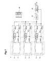
- Fig. 1 is an overall diagram of a photodetector 1 in accordance with an embodiment.
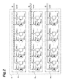
- Fig. 2 is a partial diagram of the photodetector 1 in accordance with the embodiment.
- Fig. 3 is a circuit diagram of an electric charge amount level determining circuit 10 m,n and an integrating circuit 20 m which are included in the photodetector I in accordance with the embodiment.
- Fig. 4 is a timing chart for explaining operations of the photodetector I in accordance with the embodiment.
- Fig. 5 is a timing chart for explaining operations of the photodetector 1 in accordance with the embodiment in more detail.
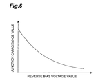
- Fig. 6 is a graph showing the relationship between the reverse bias voltage and junction capacitance value in a photodiode.
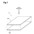
- Fig. 7 is a perspective view showing the relationship of arrangement of a first substrate 100 and a second substrate 200 in the photodetector 1 in accordance with the embodiment.
- Fig. 8 is a view showing an example of cross sections of the first substrate 100 and second substrate 200 in the photodetector 1 in accordance with the embodiment.
- Fig. 9 is a view showing another example of cross sections of the first substrate 100 and second substrate 200 in the photodetector 1 in accordance with the embodiment.
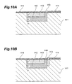
- Fig. 10A is an explanatory view of a first example of buried photodiode.
- Fig. 10B is an explanatory view of a second example of buried photodiode.
- Fig. 1 is an overall diagram of a photodetector 1 in accordance with an embodiment.
- Fig. 2 is a partial diagram of the photodetector 1 in accordance with this embodiment.
- Fig. 2 shows details of blocks X 1 to X M within the area Y indicated by dotted lines in Fig. 1.
- the photodetector 1 shown in these drawings comprises M units U 1 to U M , an A/D converter 30, a shift circuit 40, and a control circuit 50.
- Each unit U m has the same configuration comprising N photodiodes PD m,1 to PD m,N, N electric charge amount level determining circuits 10 m,1 to 10 m,N , N first switches SW1 m,1 to SW1 m,N, N second switches SW2 m,1 to SW2 m,N, an integrating circuit 20 m , a switch SW3 m , and a switch SW4 m .
- M is an integer of 1 or greater
- N is an integer of 2 or greater
- m is an integer of at least 1 but not greater than M
- n in the following is an integer of at least I but not greater than N.
- Each photodiode PD m,n is a photodiode having an anode terminal and a cathode terminal (a reverse bias voltage is applied between the anode terminal and the cathode terminal), generating electric charges Q by an amount corresponding to the incident light intensity, and accumulating thus generated electric charges Q into a junction capacitance part.
- Each switch SW1 m,n is arranged between its corresponding photodiode PD m,n and the input terminal of the integrating circuit 20 m , and can electrically be opened and closed.
- Each electric charge amount level determining circuit 10 m,n is provided for its corresponding photodiode PD m,n, determines the level of the amount of electric charges Q generated in the photodiode PD m,n and accumulated in the junction capacitance part, and outputs a level signal Level indicative of the result of level determination.
- Switch SW2 m,n is arranged between its corresponding electric charge amount level determining circuit 10 m,n and the integrating circuit 20 m , and can electrically be opened and closed.
- the level signal Level is a digital signal of 1 bit or a plurality of bits, whereas the switch SW2 m,n includes switches by a number corresponding to that of the bits.
- the integrating circuit 20 m includes an integral capacitance part having a variable capacitance value, whose input terminal is connected to the photodiodes PD m,n by way of their corresponding switches SW1 m,n .
- the switches SW1 m,1 to SW1 m,N are sequentially opened and closed, the respective electric charges Q are sequentially outputted from the N photodiodes PD m,1 to PD m,N , so as to be fed into the input terminal and accumulated into the integral capacitance part, whereby a voltage V 20 corresponding to the amount of thus accumulated electric charges Q is outputted from an output terminal.
- the integral capacitance part is connected to the electric charge amount level determining circuits 10 m,n by way of their corresponding switches SW2 m,n .
- the switches SW2 m,1 to SW2 m,N are sequentially opened and closed, the level signals Level are sequentially inputted from the N electric charge amount level determining circuits 10 m,n . According to thus inputted level signals Level, the capacitance value is set.
- the A/D converter circuit 30 receives inputs of the voltages V 20 sequentially outputted from the output terminals of the integrating circuits 20 m by way of the switches SW3 m , A/D-converts the voltage V 20 into digital values, and outputs the digital values corresponding to the voltages V 20 .
- the shift circuit 40 receives inputs of the digital values outputted from the A/D converter circuit 30, sequentially receives inputs of the respective level signals Level outputted from the electric charge amount level determining circuits 10 m,1 to 10 m,N by way of the switches SW2 m,n and switches SW4 m , shifts the bits of the digital values according to the level signals Level, and outputs thus bit-shifted digital values.
- the control circuit 50 regulates operations of the photodetector 1 as a whole. In particular, the control circuit 50 regulates the opening and closing of each of the switches SW1 m,n and SW2 m,n . Specifically, for each photodiode PD m,n , the control circuit 50 closes the corresponding switch SW2 m,n and, after the capacitance value of the integral capacitance part in the integrating circuit 20 m is set according to the level signal Level outputted from the corresponding electric charge amount level determining circuit 10 m,n, closes the corresponding switch SW1 m,n, thereby starting an integrating operation in the integrating circuit 20 m .
- the control circuit 50 also regulates timings of respective operations of the integrating circuits 20 m , switches SW3 m , switches SW4 m , A/D converter circuit 30, and shift circuit 40. These operation timings will later be explained in detail.
- Fig. 1 omits control signals sent from the control circuit 50 to the other constituent circuits.
- Fig. 3 is a circuit diagram of the electric charge amount level determining circuit 10 m,n and integrating circuit 20 m included in the photodetector 1 in accordance with this embodiment. This diagram shows only the part corresponding to the n-th photodiode PD m,n within the m-th unit U m .
- the electric charge amount level determining circuit 10 m,n includes three comparators 11 to 13 and a controller 14.
- the non-inverting input terminal of each of the comparators 11 to 13 is connected to the junction between the cathode terminal of the photodiode PD m,n and the switch SW1 m,n .
- Reference voltages V ref1 , V ref2 , and V ref3 are fed to the inverting input terminals of the comparators 11, 12, and 13, respectively.
- Each of the comparators 11 to 13 compares the respective voltages fed to its inverting and non-inverting input terminals in terms of magnitude, and outputs a signal indicative of the result of comparison to the controller 14.
- the controller 14 receives inputs of the respective signals outputted from the comparators 11 to 13, and outputs a 3-bit level signal Level for setting the capacitance value of the integral capacitance part in the integrating circuit 20 m .
- V ref 1 V sat /2
- V ref 2 V sat /4
- V ref 3 V sat /8
- V sat is a constant value. Therefore, the three comparators 11 to 13 can determine within which of the following ranges: V PD ⁇ V sat / 8 V sat /8 ⁇ V PD ⁇ V sat /4 V sat /4 ⁇ V PD ⁇ V sat /2 V sat /2 ⁇ V PD the potential V PD of the cathode terminal of the photodiode PD m,n falls.
- the level signal Level outputted from the controller 14 indicates within which ranges of the above-mentioned expressions (2a) to (2d) the potential V PD falls.
- the integrating circuit 20 m includes an amplifier A, capacitance elements C 0 to C 3 , and switches SW 0 to SW 3 .
- the amplifier A includes a non-inverting input terminal, an inverting input terminal, and an output terminal.
- the non-inverting input terminal and the inverting input terminal of the amplifier A form a virtual short circuit therebetween, thus yielding potentials identical to each other.
- the non-inverting input terminal receives inputs of a voltage V inp .
- the voltage V inp is not constant but variable. For example, one of a constant voltage V H from a first constant voltage source and a constant voltage V L from a second constant voltage source (V L ⁇ V H ) is selectively fed to the non-inverting input terminal of the amplifier A.
- the inverting input terminal of the amplifier A is connected to the cathode terminal of the photodiode PD m,n by way of the switch SW1 m,n .
- the output terminal of the amplifier A is connected to the A/D converter circuit 30 by way of the switch SW3 m .
- the switch SW 1 and capacitance element C 1 connected in series, the switch SW 2 and capacitance element C 2 connected in series, the switch SW 3 and capacitance element C 3 connected in series, the capacitance element C 0 , and the switch SW 0 are connected in parallel between the inverting input terminal and the output terminal of the amplifier A.
- the capacitance elements C 0 to C 3 and switches SW 1 to SW 3 constitute an integral capacitance part 21 having a variable capacitance value. Namely, the switches SW 1 to SW 3 open and close depending on the level signal Level inputted from the controller 14 of the electric charge amount level determining circuit 10 m,n by way of the switch SW2 m,n , whereby the capacitance value of the integral capacitance part 21 is determined according to their states of opening/closing.
- C is a constant value.
- the A/D converter circuit 30 receives inputs of the voltages V 20 sequentially arriving from the respective output terminals 20 m of the units U m by way of the switches SW3 m , A/D-converts the voltages V 20 , and outputs digital values corresponding to the voltages V 20 .
- the voltages V 20 fed into the A/D converter circuit 30 always fall within the above-mentioned expression (4), whereby the A/D converter circuit 30 can effectively utilize all the bits of its outputting digital values when A/D-converting the voltages V 20 .
- the shift circuit 40 receives inputs of the digital values outputted from the A/D converter circuit 30, sequentially receives inputs of the respective level signals Level outputted from the electric charge amount level determining circuits 10 m,1 to 10 m,N , shifts the bits of digital values according to the level signals Level, and outputs the bit-shifted digital values. Namely, when a digital value outputted from the A/D converter circuit 30 is a digital value (D K-1 , D K-2 , ..., D 1 , D 0 ) having K bits (where K is an integer of 2 or greater), the shift circuit 40 outputs a digital value having (K + 3) bits.
- the shift circuit 40 When the level signal Level indicates that the potential V PD falls within the range of the above-mentioned expression (2a), the shift circuit 40 outputs the digital value (0, 0, 0, D K-1 , D K-2 , ..., D 1 , D 0 ) having (K + 3) bits without shifting the bits of the inputted digital value.
- the shift circuit 40 shifts the inputted digital value by 1 bit to the higher order, and outputs thus obtained digital value (0, 0, D K-1 , D K-2 , ..., D 1 , D 0 , 0) having (K + 3) bits.
- the shift circuit 40 shifts the inputted digital value by 2 bits to the higher order, and outputs thus obtained digital value (0, D K-1 , D K-2 , ..., D 1 , D 0 , 0, 0) having (K + 3) bits.
- the shift circuit 40 shifts the inputted digital value by 3 bits to the higher order, and outputs thus obtained digital value (D K-1 , D K-2 , ..., D 1 , D 0 , 0, 0, 0) having (K + 3) bits.
- Fig. 4 is a timing chart for explaining operations of the photodetector 1 in accordance with this embodiment.
- This chart shows, successively from the upper side, respective opening/closing timings of the switches SW2 m,n-1 and SW1 m,n-1 corresponding to the photodiode PD m,n-1 , respective opening/closing timings of the switches SW2 m,n and SW1 m,n corresponding to the photodiode PD m,n arranged adjacent to the PD m,n-1 in each unit U m , respective opening/closing timings of the switches SW2 m,n+1 and SW1 m,n+1 corresponding to the photodiode PD m,n+1 arranged adjacent to the PD m,n in each unit U m , the output voltage V 20 from the integrating circuit 20 m , and output digital values from the A/D converter circuit 30.
- the level signal at this time indicates the level of the potential V PD of the cathode terminal of the photodiode PD m,n determined by the three comparators 11 to 13 of the electric charge amount level determining circuit 10 m,n-1 and held by the controller 14 at the time t n-1,2 .
- the switch SW 0 of the integrating circuit 20 m is closed at the time t n-1,2 , so that the voltage V 20 outputted from the integrating circuit 20 m is initialized.
- the M switches SW3 m are closed sequentially, and the M switches SW4 m are closed sequentially.
- the voltages V 20 sequentially outputted from the M units U 1 to U M are converted into digital values by the A/D converter circuit 30, whereas these digital values are outputted from the shift circuit 40 after being bit-shifted thereby according to the level signals Level sequentially outputted from the M units U 1 to U M .
- the digital values sequentially outputted from the shift circuit 40 at this time correspond to respective intensities of light incident on the n-th photodiodes PD m,n included in the M units U 1 to U M .
- the n-th switches SW1 m,n and SW2 m,n are opened in each unit U m , whereas the switch SW 0 in the integrating circuit 20 m is closed, whereby a series of operations concerning the n-th photodiode PD m,n end.
- a series of operations concerning the (n+1)-th photodiode PD m,n+1 are similarly carried out in each unit U m . The same holds in subsequent periods.
- Fig. 5 is a timing chart for explaining operations of the photodetector 1 in accordance with this embodiment in more detail.
- This chart shows, successively from the upper side, the opening/closing timing of the switch SW1 m,n, the opening/closing timing of the switch SW 0 in the integrating circuit 20 m , the output voltage V 20 from the integrating circuit 20 m , and the voltage V inp fed to the non-inverting input terminal of the amplifier A in the integrating circuit 20 m .
- the switch SW1 m,n is open, and the switch SW 0 in the integrating circuit 20 m is also open.
- the voltage V inp fed to the non-inverting input terminal of the amplifier A in the integrating circuit 20 m is the lower voltage V L .
- the switch SW 0 of the integrating circuit 20 m is closed, whereby the output voltage V 20 from the integrating circuit 20 m is initialized.
- the voltage V inp fed to the non-inverting input terminal of the amplifier A in the integrating circuit 20 m changes from the lower voltage V L to the higher voltage V H .
- the switch SW 0 of the integrating circuit 20 m is opened, so that the integrating circuit 20 m is placed in a condition enabling an operation of accumulating electric charges.
- the switch SW1 m,n is closed at time t c , the electric charges accumulated in the junction capacitance part of the photodiode PD m,n so far are fed into the integrating circuit 20 m by way of the switch SW1 m,n, so as to be accumulated into the integral capacitance part 21 of the integrating circuit 20 m , whereby the integrating circuit 20 m outputs the voltage V 20 corresponding to the amount of electric charges accumulated in the integral capacitance part 21.
- the switch SW 0 of the integrating circuit 20 m is closed, so that the electric charge accumulating operation in the integrating circuit 20 m is terminated, whereby the output voltage V 20 from the integrating circuit 20 m is initialized.
- the voltage V inp fed to the non-inverting input terminal of the amplifier A in the integrating circuit 20 m changes from the higher voltage V H to the lower voltage V L .
- the switch SW1 m,n is opened, and the switch SW 0 of the integrating circuit 20 m is also opened.
- the voltage V inp fed to the non-inverting input terminal of the amplifier A in the integrating circuit 20 in is switched from the lower voltage V L to the higher voltage V H or vice versa in the period during which the switch SW 0 of the integrating circuit 20 m is closed (the period during which the output voltage from the integrating circuit 20 m is initialized), whereby the output voltage of the integrating circuit 20 m is not affected thereby.
- the lower voltage V L is fed as the voltage V inp to the non-inverting input terminal of the amplifier A in the integrating circuit 20 m in the first period (before the time t a and after the time t e ) during which the junction capacitance part of the photodiode PD m,n accumulates electric charges
- the higher voltage V H is fed as the voltage V inp to the non-inverting input terminal of the amplifier A in the integrating circuit 20 m in the second period (times t c to t d ) during which the integral capacitance part 21 of the integrating circuit 20 m accumulates electric charges.
- the junction capacitance value is smaller as the reverse bias voltage of a photodiode is greater. Therefore, as compared with the first period, a greater reverse bias voltage is applied to the photodiode PD m,n whereas the junction capacitance value of PD m,n becomes smaller in the second period.
- means for changing the voltage V inp fed to the non-inverting input terminal of the amplifier A in the integrating circuit 20 m acts as reverse bias voltage changing means.
- the junction capacitance value of the photodiode PD m,n is greater in the first period during which the junction capacitance part of the photodiode PD m,n accumulates electric charges, whereby the junction capacitance part of the photodiode PD m,n can accumulate a greater number of electric charges.
- the junction capacitance value of the photodiode PD m,n is smaller, so that the migration of electric charges from the junction capacitance part of the photodiode PD m,n to the integral capacitance part 21 of the integrating circuit 20 m can be carried out at a high speed with a low noise.
- the photodetector 1 in accordance with this embodiment can improve each of the dynamic range, S/N ratio, and speed of light detection.
- each photodiode PD m,n is provided with the electric charge amount level determining circuit 10 m,n in the photodetector 1 in accordance with this embodiment, an appropriate capacitance value corresponding to the amount of electric charges outputted from the photodiode PD m,n is set in the integral capacitance part 21 of the integrating circuit 20 m , whereby the dynamic range of incident light intensity detection for each photodiode (i.e., per pixel in one picture) can be enlarged.
- the capacitance value of the integral capacitance part 21 in the integrating circuit 20 m can be set rapidly, whereby the incident light intensity can be detected with a high speed. Also, since each electric charge amount level determining circuit 10 m,n does not require high-speed processing when determining the electric charge amount level, the power consumption can be saved.
- FIG. 7 is a perspective view showing the relationship of arrangement of a first substrate 100 and a second substrate 200 in the photodetector 1 in accordance with this embodiment.
- the photodetector 1 is split onto two substrates, i.e., the first substrate 100 and the second substrate 200.
- M x N photodiodes PD 1,1 to PD M,N are arranged in a matrix of M rows by N columns.
- M x N electric charge amount level determining circuits 10 1,1 to 10 M,N, M x N switches SW1 1,1 to SW1 M,N, M x N switches SW2 1,1 to SW2 M,N, M integrating circuits 20 1 to 20 M , M switches SW3 1 to SW3 M , M switches SW4 1 to SW4 M , an A/D converter circuit 30, a shift circuit 40, and a control circuit 50 are arranged. As shown in Fig. 7, the substrates are mounted while being laminated such that they are overlaid on each other in the light incidence direction.
- the respective cathode electrodes of the photodiodes PD m,n on the first substrate 100 are electrically connected to their corresponding switches SW1 m,n and electric charge amount level determining circuits 10 m,n on the second substrate 200 by way of bumps.
- Fig. 8 is a view showing an example of cross sections of the first substrate 100 and second substrate 200 in the photodetector 1 in accordance with this embodiment. Since a basic pattern is repeated in the lateral direction in this drawing, only one basic pattern will be explained in the following.
- n + region 111 Formed on a first surface (the upper face in the drawing) of an n-type semiconductor substrate in the first substrate 100 are a p + region 111 constructing a photodiode PD by forming a pn junction with the n-type substrate, and an n + region 112 as an isolation region.
- n + -type impurity layer 121 Formed on a second surface (the lower face in the drawing) of the n-type semiconductor substrate in the first substrate 100 are an n + -type impurity layer 121 forming an ohmic connection with a bonding pad 124, an insulating protective layer 122 for protecting the surface, and the bonding pad 124 penetrating through the protective layer 122 so as to be electrically connected to the n + -type impurity layer 121.
- a through hole is formed so as to penetrate through the first substrate 100 between the first and second surfaces, whereas a through electrode 131 is arranged within the through hole by way of an insulator layer formed on the inner wall.
- a metal lead 113 for electrically connecting the p + region 111 to the through electrode 131 is formed on an insulating film 114 on the first surface side of the first substrate 100, whereas a bonding pad 123 electrically connected to the through electrode 131 is formed on the second surface side.
- a bonding pad 223 electrically connected to a first terminal of a switch SW1, and a bonding pad 224 electrically connected to a ground potential.
- the bonding pad 123 of the first substrate 100 and the bonding pad 223 of the second substrate 200 are connected to each other with a bump 423, whereas the bonding pad 124 of the first substrate 100 and the bonding pad 224 of the second substrate 200 are connected to each other with a bump 424.
- the gap between the first substrate 100 and second substrate 200 is filled with a resin.
- a scintillator 510 and a shield plate 520 are arranged on the first surface side of the first substrate 100.
- the scintillator 510 is arranged above the p + region 111 of the first substrate 100, and generates scintillation light when energy lines such as X-rays are incident thereon.
- the shield plate 520 which is arranged above the n + region 112 of the first substrate 100, inhibits energy lines such as X-rays from penetrating therethrough and secures the scintillator 510.
- the scintillator 510 When energy lines such as X-rays are incident on the scintillator 510 in the configuration shown in Fig. 8, the scintillator 510 generates scintillation light.
- the scintillation light When the scintillation light is incident on the p + region 111 of the first substrate 100, electric charges are generated in its pn junction electric charges generate. These electric charges pass the metal lead 113, the through electrode 131, the bonding pad 123, the bump 423, and the bonding pad 223 of the second substrate 200, so as to be fed to the input terminal of the integrating circuit 20 by way of the switch SW1 formed on the second substrate 200.
- Fig. 9 is a view showing another example of cross sections of the first substrate 100 and second substrate 200 in the photodetector 1 in accordance with this embodiment. Since a basic pattern is also repeated in the lateral direction in this drawing, only one basic pattern will be explained in the following.
- n + -type accumulation layer 151 for preventing electric charges from recombining
- an insulating protective layer 152 for protecting the surface.
- a second surface (the lower face in the drawing) of the n-type semiconductor substrate in the first substrate 100 are a p + region 161 forming a pn junction with the n-type substrate so as to construct a photodiode PD, and an n + region 162 as an isolation region, whereas a protective layer 163 is formed on them.
- a bonding pad 164 electrically connected to the p + region 161
- a bonding pad 165 electrically connected to the n + region 162.
- bonding pads 264 electrically connected to a first terminal of the switch SW1, and a bonding pad 265 electrically connected to a ground potential.
- the bonding pad 164 of the first substrate 100 and the bonding pad 264 of the second substrate 200 are connected to each other with a bump 464.
- the bonding pad 165 of the first substrate 100 and the bonding pad 265 of the second substrate 200 are connected to each other with a bump 465.
- the gap between the first substrate 100 and second substrate 200 is filled with a resin.
- a scintillator 510 and a shield plate 520 are arranged on the first surface side of the first substrate 100.
- the scintillator 510 is arranged above the p + region 161 of the first substrate 100, and generates scintillation light when energy lines such as X-rays are incident thereon.
- the shield plate 520 which is arranged above the n + region 162 of the first substrate 100, inhibits energy lines such as X-rays from penetrating therethrough and secures the scintillator 510.
- the first substrate 100 is etched on the first surface side in the part formed with the p + region 161, so as to be thinned.
- the scintillator 510 When energy lines such as X-rays are incident on the scintillator 510 in the configuration shown in Fig. 9, the scintillator 510 generates scintillation light.
- the scintillation light When the scintillation light is incident on the p + region 161 through the first substrate 100, electric charges are generated in the pn junction. These electric charges pass the bonding pad 164, the bump 464, and the bonding pad 264 of the second substrate 200, and are fed to the input terminal of the integrating circuit 20 by way of the switch SW1 formed on the second substrate 200.
- the photodetector 1 in accordance with this embodiment constructed as in the foregoing can exhibit the following effects. Namely, the electric charge migration path from each photodiode PD m,n to the input termianl of the integrating circuit 20 m becomes shorter, so that the parasitic capacitance in the wiring on the path becomes smaller, which reduces the noise included in the voltage outputted from the integrating circuit 20 m , thereby making it possible to detect light accurately. Since circuits for signal processing such as the integrating circuit 20 m are not provided on the first substrate 100, an increase in the number of pixels or a higher density can be achieved.
- the second substrate 200 can be made smaller than the first substrate 100, so that, when arranging a plurality of photodetectors 1, the first substrates 100 each provided with a photodiode can be arranged very close to each other or in contact with each other. It is also favorable in that respective optimal processes can be employed for the first substrate 100 formed with a photodiode array and the second substrate 200 formed with a signal processing circuit such as the integrating circuit 20 m .
- each photodiode has a general configuration in Figs. 8 and 9 explained in the foregoing, buried photodiodes such as those shown in Figs. 10A and 10B are also favorable.
- the buried photodiode whose cross-sectional configuration is shown in Fig. 10A includes a p region 141, an n - region 142 on the p region 141, and a p + region 143 on the n - region 142.
- the p region 141 and n - region 142 form a pn junction, whereas the n - region 142 and p + region 143 also form a pn junction.
- the n - region 142 is electrically connected to the metal lead 113.
- the buried photodiode whose cross-sectional configuration is shown in Fig. 10B includes a p region 141, an n - region 142 on the p region 141, a p + region 143 on the n- region 142, and an n + region 144 in contact with the n - region 142.
- the p region 141 and n - region 142 form a pn junction, whereas the n - region 142 and p + region 143 also form a pn junction.
- the n - region 142 is electrically connected to the metal lead 113.
- the p region 141 and n - region 142 form a pn junction, whereas the n - region 142 and p + region 143 also form a pn junction.
- the n + region 144 is electrically connected to the metal lead 113.
- a buried photodiode as such is also effective in improving the S/N ratio of light detection in that leak currents are restrained from generating. Since the photodiode can completely be depleted by increasing the reverse bias voltage thereof in the second period during which the integral capacitance part 21 of the integrating circuit 20 m accumulates electric charges, the junction capacitance value in the photodiode can be made substantially zero, which is also effective in improving the S/N ratio and speed of light detection.
- the present invention can be modified in various manners.
- the cross-sectional structures of the first substrate 100 and second substrate 200 are not restricted to those shown in Figs. 8 and 9.
- Other circuits may also be provided on the second substrate 200.
- the number of thresholds for determining the electric charge amount level in the electric charge amount level determining circuit 10 m,n is arbitrary. Depending on this number, the number of cases of capacitance values attainable by the integral capacitance part of the integrating circuit 20 m is determined.
- the value of reverse bias voltage applied to the photodiode is made greater in the second period during which the integral capacitance part of the integrating circuit accumulates electric charges than in the first period during which the junction capacitance part of the photodiode accumulates electric charges.
- this photodetector can improve each of the dynamic range, S/N ratio, and speed of light detection.
Landscapes
- Engineering & Computer Science (AREA)
- Multimedia (AREA)
- Signal Processing (AREA)
- Power Engineering (AREA)
- Physics & Mathematics (AREA)
- General Physics & Mathematics (AREA)
- Spectroscopy & Molecular Physics (AREA)
- Photometry And Measurement Of Optical Pulse Characteristics (AREA)
- Transforming Light Signals Into Electric Signals (AREA)
- Solid State Image Pick-Up Elements (AREA)
- Light Receiving Elements (AREA)
Applications Claiming Priority (3)
| Application Number | Priority Date | Filing Date | Title |
|---|---|---|---|
| JP2002375130 | 2002-12-25 | ||
| JP2002375130A JP3977735B2 (ja) | 2002-12-25 | 2002-12-25 | 光検出装置 |
| PCT/JP2003/016801 WO2004059748A1 (ja) | 2002-12-25 | 2003-12-25 | 光検出装置 |
Publications (3)
| Publication Number | Publication Date |
|---|---|
| EP1577955A1 true EP1577955A1 (de) | 2005-09-21 |
| EP1577955A4 EP1577955A4 (de) | 2009-08-19 |
| EP1577955B1 EP1577955B1 (de) | 2013-12-11 |
Family
ID=32677327
Family Applications (1)
| Application Number | Title | Priority Date | Filing Date |
|---|---|---|---|
| EP03782900.9A Expired - Lifetime EP1577955B1 (de) | 2002-12-25 | 2003-12-25 | Optischer sensor |
Country Status (6)
| Country | Link |
|---|---|
| US (1) | US7442911B2 (de) |
| EP (1) | EP1577955B1 (de) |
| JP (1) | JP3977735B2 (de) |
| CN (1) | CN100407444C (de) |
| AU (1) | AU2003292622A1 (de) |
| WO (1) | WO2004059748A1 (de) |
Cited By (1)
| Publication number | Priority date | Publication date | Assignee | Title |
|---|---|---|---|---|
| CN102889927A (zh) * | 2011-07-20 | 2013-01-23 | 精工电子有限公司 | 光检测装置 |
Families Citing this family (16)
| Publication number | Priority date | Publication date | Assignee | Title |
|---|---|---|---|---|
| JP4663956B2 (ja) * | 2002-12-25 | 2011-04-06 | 浜松ホトニクス株式会社 | 光検出装置 |
| JP4314172B2 (ja) * | 2004-08-30 | 2009-08-12 | シャープ株式会社 | 増幅型固体撮像装置 |
| JP4416668B2 (ja) * | 2005-01-14 | 2010-02-17 | キヤノン株式会社 | 固体撮像装置、その制御方法及びカメラ |
| JP2008258885A (ja) * | 2007-04-04 | 2008-10-23 | Texas Instr Japan Ltd | 撮像装置および撮像装置の駆動方法 |
| US8044943B2 (en) * | 2008-06-03 | 2011-10-25 | Himax Technologies Limited | Touch panel |
| WO2010058369A2 (en) * | 2008-11-24 | 2010-05-27 | Philips Intellectual Property & Standards Gmbh | X-ray detector |
| JP2013110282A (ja) * | 2011-11-21 | 2013-06-06 | Canon Inc | 発光素子の駆動回路および発光装置 |
| JP5986443B2 (ja) * | 2012-07-13 | 2016-09-06 | 富士フイルム株式会社 | 放射線画像撮影装置、放射線の照射開始の検出感度の制御方法およびプログラム |
| JP5925711B2 (ja) * | 2013-02-20 | 2016-05-25 | 浜松ホトニクス株式会社 | 検出器、pet装置及びx線ct装置 |
| CN111263885B (zh) | 2017-09-19 | 2024-12-06 | 拜克门寇尔特公司 | 用于化学发光测量中的模拟光测量和光子计数的系统 |
| US11181419B2 (en) * | 2018-10-09 | 2021-11-23 | Omnivision Technologies, Inc. | Photon sensing with threshold detection using capacitor-based comparator |
| JP2024528463A (ja) * | 2021-06-22 | 2024-07-30 | 上海禾賽科技有限公司 | 光検出回路及び方法、レーザーレーダー、記憶媒体並びに検出システム |
| JP7762519B2 (ja) * | 2021-08-18 | 2025-10-30 | ローム株式会社 | 近接センサ及び電子機器 |
| JP7844189B2 (ja) | 2022-02-28 | 2026-04-13 | キヤノン株式会社 | 光電変換装置および機器 |
| CN115436349B (zh) * | 2022-08-17 | 2026-06-30 | 中国科学院大连化学物理研究所 | 一种具备电荷富集的光电二极管电流检测装置及方法 |
| CN121721689B (zh) * | 2026-02-27 | 2026-05-08 | 陕西卫峰核电子有限公司 | 一种α、β表面污染探测器漏光检测方法和装置 |
Family Cites Families (16)
| Publication number | Priority date | Publication date | Assignee | Title |
|---|---|---|---|---|
| JP2639654B2 (ja) | 1987-03-27 | 1997-08-13 | 株式会社 半導体エネルギ−研究所 | イメージセンサー駆動方法 |
| JPH03195278A (ja) | 1989-12-25 | 1991-08-26 | Nec Corp | 固体撮像装置の光電変換制御方法 |
| JP2810525B2 (ja) | 1990-11-06 | 1998-10-15 | キヤノン株式会社 | 光電変換装置の駆動方法 |
| JP2743842B2 (ja) | 1994-08-29 | 1998-04-22 | 日本電気株式会社 | 赤外線検出器 |
| CN1091302C (zh) * | 1995-04-05 | 2002-09-18 | 松下电器产业株式会社 | 光检测装置及其制造方法 |
| US5920070A (en) * | 1996-11-27 | 1999-07-06 | General Electric Company | Solid state area x-ray detector with adjustable bias |
| US5900623A (en) | 1997-08-11 | 1999-05-04 | Chrontel, Inc. | Active pixel sensor using CMOS technology with reverse biased photodiodes |
| WO2000014960A1 (en) * | 1998-09-09 | 2000-03-16 | Hamamatsu Photonics K.K. | Solid-state camera |
| JP4212070B2 (ja) * | 1998-09-18 | 2009-01-21 | 富士フイルム株式会社 | 固体撮像素子及びその制御方法 |
| JP2001291877A (ja) * | 2000-04-05 | 2001-10-19 | Hamamatsu Photonics Kk | 固体撮像装置 |
| JP4489914B2 (ja) * | 2000-07-27 | 2010-06-23 | 浜松ホトニクス株式会社 | A/d変換装置および固体撮像装置 |
| US7286172B2 (en) * | 2000-08-03 | 2007-10-23 | Hamamatsu Photonics K.K. | Optical sensor |
| JP3844699B2 (ja) * | 2001-02-19 | 2006-11-15 | イノテック株式会社 | 可変利得アンプ |
| JP4722332B2 (ja) * | 2001-06-18 | 2011-07-13 | 浜松ホトニクス株式会社 | 光検出装置 |
| JP3976185B2 (ja) * | 2001-10-31 | 2007-09-12 | シャープ株式会社 | 受光素子、回路内蔵受光素子および光ピックアップ |
| US6908779B2 (en) * | 2002-01-16 | 2005-06-21 | Matsushita Electric Industrial Co., Ltd. | Semiconductor device and method for manufacturing the same |
-
2002
- 2002-12-25 JP JP2002375130A patent/JP3977735B2/ja not_active Expired - Fee Related
-
2003
- 2003-12-25 US US10/540,748 patent/US7442911B2/en not_active Expired - Fee Related
- 2003-12-25 WO PCT/JP2003/016801 patent/WO2004059748A1/ja not_active Ceased
- 2003-12-25 CN CN2003801077833A patent/CN100407444C/zh not_active Expired - Fee Related
- 2003-12-25 AU AU2003292622A patent/AU2003292622A1/en not_active Abandoned
- 2003-12-25 EP EP03782900.9A patent/EP1577955B1/de not_active Expired - Lifetime
Cited By (2)
| Publication number | Priority date | Publication date | Assignee | Title |
|---|---|---|---|---|
| CN102889927A (zh) * | 2011-07-20 | 2013-01-23 | 精工电子有限公司 | 光检测装置 |
| CN102889927B (zh) * | 2011-07-20 | 2015-12-09 | 精工电子有限公司 | 光检测装置 |
Also Published As
| Publication number | Publication date |
|---|---|
| EP1577955B1 (de) | 2013-12-11 |
| CN1732574A (zh) | 2006-02-08 |
| WO2004059748A1 (ja) | 2004-07-15 |
| JP2004207505A (ja) | 2004-07-22 |
| US20060261254A1 (en) | 2006-11-23 |
| JP3977735B2 (ja) | 2007-09-19 |
| AU2003292622A1 (en) | 2004-07-22 |
| EP1577955A4 (de) | 2009-08-19 |
| CN100407444C (zh) | 2008-07-30 |
| US7442911B2 (en) | 2008-10-28 |
Similar Documents
| Publication | Publication Date | Title |
|---|---|---|
| US20090184237A1 (en) | Photodetector | |
| US7442911B2 (en) | Photodector including photodiodes having improved dynamic range, s/n ratio and speed of light detection | |
| EP2549537B1 (de) | Lichterkennungsvorrichtung | |
| US6665013B1 (en) | Active pixel sensor having intra-pixel charge transfer with analog-to-digital converter | |
| US20190141270A1 (en) | Solid-state imaging device, method for driving solid-state imaging device, and electronic apparatus | |
| US4233632A (en) | Solid state image pickup device with suppressed so-called blooming phenomenon | |
| EP3540773B1 (de) | Lichtdetektionsvorrichtung | |
| US7800667B2 (en) | Photo-detecting apparatus | |
| US20090173874A1 (en) | Optoelectronic Detector with Multiple Readout Nodes and Its Use Thereof | |
| EP0187047A2 (de) | Bildsensoranordnung | |
| US20060077269A1 (en) | Pixel binning image sensor | |
| US8018515B2 (en) | Solid-state image pickup device | |
| US7679663B2 (en) | Photodetection apparatus | |
| EP1712886B1 (de) | Photodetektorbauelement | |
| JP2021150742A (ja) | イメージセンサ |
Legal Events
| Date | Code | Title | Description |
|---|---|---|---|
| PUAI | Public reference made under article 153(3) epc to a published international application that has entered the european phase |
Free format text: ORIGINAL CODE: 0009012 |
|
| 17P | Request for examination filed |
Effective date: 20050620 |
|
| AK | Designated contracting states |
Kind code of ref document: A1 Designated state(s): AT BE BG CH CY CZ DE DK EE ES FI FR GB GR HU IE IT LI LU MC NL PT RO SE SI SK TR |
|
| AX | Request for extension of the european patent |
Extension state: AL LT LV MK |
|
| DAX | Request for extension of the european patent (deleted) | ||
| RBV | Designated contracting states (corrected) |
Designated state(s): DE FR GB NL |
|
| A4 | Supplementary search report drawn up and despatched |
Effective date: 20090720 |
|
| 17Q | First examination report despatched |
Effective date: 20090730 |
|
| REG | Reference to a national code |
Ref country code: DE Ref legal event code: R079 Ref document number: 60345432 Country of ref document: DE Free format text: PREVIOUS MAIN CLASS: H01L0031100000 Ipc: G01J0001460000 |
|
| GRAP | Despatch of communication of intention to grant a patent |
Free format text: ORIGINAL CODE: EPIDOSNIGR1 |
|
| RIC1 | Information provided on ipc code assigned before grant |
Ipc: G01J 1/46 20060101AFI20130523BHEP Ipc: H04N 3/14 20060101ALI20130523BHEP Ipc: H04N 5/355 20110101ALI20130523BHEP Ipc: H04N 5/378 20110101ALI20130523BHEP Ipc: H01L 27/146 20060101ALI20130523BHEP |
|
| INTG | Intention to grant announced |
Effective date: 20130625 |
|
| GRAS | Grant fee paid |
Free format text: ORIGINAL CODE: EPIDOSNIGR3 |
|
| GRAA | (expected) grant |
Free format text: ORIGINAL CODE: 0009210 |
|
| AK | Designated contracting states |
Kind code of ref document: B1 Designated state(s): DE FR GB NL |
|
| REG | Reference to a national code |
Ref country code: GB Ref legal event code: FG4D |
|
| REG | Reference to a national code |
Ref country code: NL Ref legal event code: T3 |
|
| REG | Reference to a national code |
Ref country code: DE Ref legal event code: R096 Ref document number: 60345432 Country of ref document: DE Effective date: 20140206 |
|
| REG | Reference to a national code |
Ref country code: DE Ref legal event code: R097 Ref document number: 60345432 Country of ref document: DE |
|
| PLBE | No opposition filed within time limit |
Free format text: ORIGINAL CODE: 0009261 |
|
| STAA | Information on the status of an ep patent application or granted ep patent |
Free format text: STATUS: NO OPPOSITION FILED WITHIN TIME LIMIT |
|
| 26N | No opposition filed |
Effective date: 20140912 |
|
| REG | Reference to a national code |
Ref country code: DE Ref legal event code: R097 Ref document number: 60345432 Country of ref document: DE Effective date: 20140912 |
|
| REG | Reference to a national code |
Ref country code: FR Ref legal event code: PLFP Year of fee payment: 13 |
|
| REG | Reference to a national code |
Ref country code: FR Ref legal event code: PLFP Year of fee payment: 14 |
|
| REG | Reference to a national code |
Ref country code: FR Ref legal event code: PLFP Year of fee payment: 15 |
|
| PGFP | Annual fee paid to national office [announced via postgrant information from national office to epo] |
Ref country code: NL Payment date: 20181114 Year of fee payment: 16 |
|
| PGFP | Annual fee paid to national office [announced via postgrant information from national office to epo] |
Ref country code: DE Payment date: 20181211 Year of fee payment: 16 |
|
| PGFP | Annual fee paid to national office [announced via postgrant information from national office to epo] |
Ref country code: GB Payment date: 20181219 Year of fee payment: 16 Ref country code: FR Payment date: 20181120 Year of fee payment: 16 |
|
| REG | Reference to a national code |
Ref country code: DE Ref legal event code: R119 Ref document number: 60345432 Country of ref document: DE |
|
| REG | Reference to a national code |
Ref country code: NL Ref legal event code: MM Effective date: 20200101 |
|
| GBPC | Gb: european patent ceased through non-payment of renewal fee |
Effective date: 20191225 |
|
| PG25 | Lapsed in a contracting state [announced via postgrant information from national office to epo] |
Ref country code: NL Free format text: LAPSE BECAUSE OF NON-PAYMENT OF DUE FEES Effective date: 20200101 |
|
| PG25 | Lapsed in a contracting state [announced via postgrant information from national office to epo] |
Ref country code: GB Free format text: LAPSE BECAUSE OF NON-PAYMENT OF DUE FEES Effective date: 20191225 Ref country code: FR Free format text: LAPSE BECAUSE OF NON-PAYMENT OF DUE FEES Effective date: 20191231 Ref country code: DE Free format text: LAPSE BECAUSE OF NON-PAYMENT OF DUE FEES Effective date: 20200701 |