EP1577904B1 - Traversée haute tension avec élément pour les contrôle du champ électrique - Google Patents
Traversée haute tension avec élément pour les contrôle du champ électrique Download PDFInfo
- Publication number
- EP1577904B1 EP1577904B1 EP04405151A EP04405151A EP1577904B1 EP 1577904 B1 EP1577904 B1 EP 1577904B1 EP 04405151 A EP04405151 A EP 04405151A EP 04405151 A EP04405151 A EP 04405151A EP 1577904 B1 EP1577904 B1 EP 1577904B1
- Authority
- EP
- European Patent Office
- Prior art keywords
- field control
- bushing
- control element
- field
- mounting flange
- Prior art date
- Legal status (The legal status is an assumption and is not a legal conclusion. Google has not performed a legal analysis and makes no representation as to the accuracy of the status listed.)
- Expired - Lifetime
Links
- 230000005684 electric field Effects 0.000 title claims description 8
- 239000012212 insulator Substances 0.000 claims abstract description 66
- 239000002245 particle Substances 0.000 claims abstract description 23
- 239000011159 matrix material Substances 0.000 claims abstract description 9
- 229920001296 polysiloxane Polymers 0.000 claims abstract description 9
- 239000004593 Epoxy Substances 0.000 claims abstract description 6
- 229920002943 EPDM rubber Polymers 0.000 claims abstract description 3
- 239000011521 glass Substances 0.000 claims abstract description 3
- 229920002725 thermoplastic elastomer Polymers 0.000 claims abstract description 3
- GWEVSGVZZGPLCZ-UHFFFAOYSA-N Titan oxide Chemical compound O=[Ti]=O GWEVSGVZZGPLCZ-UHFFFAOYSA-N 0.000 claims abstract 6
- 238000012216 screening Methods 0.000 claims abstract 4
- 239000000463 material Substances 0.000 claims description 27
- 239000011248 coating agent Substances 0.000 claims description 22
- 238000000576 coating method Methods 0.000 claims description 22
- 238000011068 loading method Methods 0.000 claims description 16
- 238000009826 distribution Methods 0.000 claims description 8
- 239000007787 solid Substances 0.000 claims description 5
- 239000003990 capacitor Substances 0.000 claims description 4
- 238000009413 insulation Methods 0.000 claims description 4
- 239000007788 liquid Substances 0.000 claims description 3
- 230000001419 dependent effect Effects 0.000 claims description 2
- 229920001169 thermoplastic Polymers 0.000 claims description 2
- 239000004416 thermosoftening plastic Substances 0.000 claims description 2
- XOLBLPGZBRYERU-UHFFFAOYSA-N tin dioxide Chemical compound O=[Sn]=O XOLBLPGZBRYERU-UHFFFAOYSA-N 0.000 claims 2
- 229910002113 barium titanate Inorganic materials 0.000 claims 1
- 239000012774 insulation material Substances 0.000 claims 1
- XLOMVQKBTHCTTD-UHFFFAOYSA-N Zinc monoxide Chemical compound [Zn]=O XLOMVQKBTHCTTD-UHFFFAOYSA-N 0.000 abstract description 9
- 239000011787 zinc oxide Substances 0.000 abstract description 4
- QHGNHLZPVBIIPX-UHFFFAOYSA-N tin(ii) oxide Chemical compound [Sn]=O QHGNHLZPVBIIPX-UHFFFAOYSA-N 0.000 abstract 2
- OGIDPMRJRNCKJF-UHFFFAOYSA-N titanium oxide Inorganic materials [Ti]=O OGIDPMRJRNCKJF-UHFFFAOYSA-N 0.000 abstract 2
- 238000009434 installation Methods 0.000 abstract 1
- 239000010410 layer Substances 0.000 description 15
- 229910052573 porcelain Inorganic materials 0.000 description 9
- 239000007789 gas Substances 0.000 description 7
- 239000011347 resin Substances 0.000 description 7
- 229920005989 resin Polymers 0.000 description 7
- 239000004020 conductor Substances 0.000 description 6
- 239000011152 fibreglass Substances 0.000 description 4
- 238000005266 casting Methods 0.000 description 3
- 238000010276 construction Methods 0.000 description 3
- 238000005516 engineering process Methods 0.000 description 3
- IJGRMHOSHXDMSA-UHFFFAOYSA-N Atomic nitrogen Chemical compound N#N IJGRMHOSHXDMSA-UHFFFAOYSA-N 0.000 description 2
- 229910010413 TiO 2 Inorganic materials 0.000 description 2
- 239000002131 composite material Substances 0.000 description 2
- 239000003365 glass fiber Substances 0.000 description 2
- 238000002955 isolation Methods 0.000 description 2
- 238000000034 method Methods 0.000 description 2
- 239000003921 oil Substances 0.000 description 2
- 229920000642 polymer Polymers 0.000 description 2
- 238000004804 winding Methods 0.000 description 2
- XUIMIQQOPSSXEZ-UHFFFAOYSA-N Silicon Chemical compound [Si] XUIMIQQOPSSXEZ-UHFFFAOYSA-N 0.000 description 1
- 229910006404 SnO 2 Inorganic materials 0.000 description 1
- 239000000853 adhesive Substances 0.000 description 1
- 230000001070 adhesive effect Effects 0.000 description 1
- 239000003570 air Substances 0.000 description 1
- 239000000919 ceramic Substances 0.000 description 1
- 239000004927 clay Substances 0.000 description 1
- 238000005336 cracking Methods 0.000 description 1
- 230000001934 delay Effects 0.000 description 1
- 230000000694 effects Effects 0.000 description 1
- 238000010292 electrical insulation Methods 0.000 description 1
- 238000001125 extrusion Methods 0.000 description 1
- 239000000945 filler Substances 0.000 description 1
- 238000011049 filling Methods 0.000 description 1
- 239000006260 foam Substances 0.000 description 1
- -1 gaseous) Substances 0.000 description 1
- 239000000499 gel Substances 0.000 description 1
- 239000011810 insulating material Substances 0.000 description 1
- 239000011229 interlayer Substances 0.000 description 1
- 238000004519 manufacturing process Methods 0.000 description 1
- 239000013521 mastic Substances 0.000 description 1
- 239000002184 metal Substances 0.000 description 1
- 229910052751 metal Inorganic materials 0.000 description 1
- 229910052757 nitrogen Inorganic materials 0.000 description 1
- 238000010606 normalization Methods 0.000 description 1
- 239000003973 paint Substances 0.000 description 1
- 239000004033 plastic Substances 0.000 description 1
- 229920003023 plastic Polymers 0.000 description 1
- 239000000843 powder Substances 0.000 description 1
- 239000011241 protective layer Substances 0.000 description 1
- 238000007873 sieving Methods 0.000 description 1
- 229910052710 silicon Inorganic materials 0.000 description 1
- 239000010703 silicon Substances 0.000 description 1
- 239000002002 slurry Substances 0.000 description 1
- 238000005507 spraying Methods 0.000 description 1
- 230000007704 transition Effects 0.000 description 1
Images

Classifications
-
- H—ELECTRICITY
- H01—ELECTRIC ELEMENTS
- H01B—CABLES; CONDUCTORS; INSULATORS; SELECTION OF MATERIALS FOR THEIR CONDUCTIVE, INSULATING OR DIELECTRIC PROPERTIES
- H01B17/00—Insulators or insulating bodies characterised by their form
- H01B17/26—Lead-in insulators; Lead-through insulators
- H01B17/28—Capacitor type
-
- H—ELECTRICITY
- H01—ELECTRIC ELEMENTS
- H01B—CABLES; CONDUCTORS; INSULATORS; SELECTION OF MATERIALS FOR THEIR CONDUCTIVE, INSULATING OR DIELECTRIC PROPERTIES
- H01B17/00—Insulators or insulating bodies characterised by their form
- H01B17/42—Means for obtaining improved distribution of voltage; Protection against arc discharges
Definitions
- the invention relates to the field of high or medium voltage technology, in particular electrical insulation and connection technology for grounded high voltage apparatus. It is based on a dielectric bushing and a high-voltage electrical apparatus according to the preamble of the independent claims.
- a high voltage insulator z As porcelain or composite material with a coating of field control material (FGM) disclosed.
- the field-controlling coating consists of varistor powder, z. Of doped zinc oxide (ZnO) embedded in a polymer matrix.
- the FGM coating serves to compare the field distribution on the insulator surface and is distributed so that part of the material is in electrical contact with both the ground electrode and the high voltage electrode. In this case, the FGM coating can only partially cover the insulator length and be concentrated in the field-loaded electrode regions.
- the FGM coating can be applied to the insulator surface, can be incorporated there in a shield or can be shielded by a weatherproof, electrically insulating protective layer to the outside.
- An equalization of the capacitive field load can be realized by alternating horizontal strips or bands of FGM coating and insulator material.
- the FGM coating may be applied in the form of a glaze or a paint, or mixed into a slurry or clay, applied to the porcelain insulator and fired there to a glaze or ceramic layer.
- the matrix for the FGM coating may be a polymer, an adhesive, a casting or a mastic or a gel.
- EP 1 042 756 discloses a glass fiber reinforced insulator tube which is impregnated on the inner surface and optionally also the outer surface with a resin which has a particulate filler with varistor properties, in particular zinc oxide.
- the GRP tube can be made by winding a fiberglass mesh which is impregnated with the varistor-filled resin at least on the outer layers.
- the insulator comprises an insulator body made of porcelain or composite material and a porcelain or silicone shield.
- the shield has a variable insulator screen density.
- Isolatorend Scheme For field relief in a Isolatorend Scheme turn the known shield electrode between the insulator body and conductor is present. It is now proposed to install an increased number of insulator screens in the heavily field-loaded area where the shielding electrode ends. Due to the increased insulator screen density, improved field relief is achieved in the end region of the shield electrode.
- the invention relates to a prior art, as shown in the US Pat. 3,318,995 is known.
- cast resin bushings are disclosed, which remain electrically reliable even with differential thermal expansion or shrinkage due to cavitation between metal and cast resin.
- regions with increased cracking tendency are electrically shielded by partially conductive or semiconductive field shielding layers.
- the layers are either arranged on the high-voltage inner conductor and electrically connected to this end; or they are arranged on shielding electrodes and electrically connected to these end, wherein the shielding electrodes in turn are electrically connected to the grounded housing of the connected apparatus.
- the field shielding layers create a field-free space between themselves and the inner conductor or themselves and the shielding electrode and effectively shield cavities in the casting resin.
- the object of the present invention is to provide an improved dielectric bushing and a high-voltage electrical apparatus and an electrical switchgear with such a procedure. This object is achieved according to the invention by the features of the independent claim.
- the invention consists in a dielectric bushing, in particular a high voltage feedthrough for a high voltage electrical apparatus, comprising an insulator part with a first mounting flange and a second mounting flange for mounting the bushing, wherein within the bushing in a field loading zone in the region of the first mounting flange one for a desired voltage level required Shield electrode is omitted and instead for the purpose of field control in the field loading zone, a non-linear electrical and / or dielectric field control element on the insulator part in the region of the first mounting flange is present and the field control element is in electrical contact with the first mounting flange.
- the bushings can therefore be built shorter.
- the E-field is no longer concentrated in the region of the shielding electrode during the entire pulse duration, but can propagate as a wave along the field control element and thereby degrade.
- the maximum field strengths are reduced.
- the field control material with respect to its non-linear electrical and / or dielectric properties, its geometric shape and its arrangement on the insulator part for dielectric relief of field loading zone without shielding electrode for all operating conditions, especially for surge voltages designed.
- the field control element can thus master even the most critical field loading conditions without shielding electrode or shielding electrodes.
- design criteria for geometrical design of the field control element are specified by which an advantageous field control can be achieved with little material.
- a minimum required length of the field control element can be determined along the longitudinal extent of the insulator part according to claim 5. It is thereby achieved that the field load propagates as a traveling wave along the field control element, in particular in the case of surge voltage, and thereby degrades to such an extent that no damaging field strengths can form on reaching the remote end of the field control material.
- Claim 6 indicates how can be built with the field control element DC feedthroughs in a simple manner.
- the embodiment according to claim 7 has the advantage that in particular the highest field loads in the region of the earth flange with the field control material can be controlled.
- the embodiments according to claim 8 and 9 have the advantage that both flange regions are protected by the field control materials independently of each other from flashovers or partial discharges.
- Claim 10 feature a) indicates various radial positions for the arrangement of the field control material on the insulator part.
- Claim 10 feature b) has the advantage that a conventional GRP pipe (glass fiber reinforced plastic) or a conventional porcelain insulator by a self-supporting FGM pipe (field control material tube) is replaceable.
- Claim 11 specifies advantageous material components for the field control element.
- Claims 12 and 13 relate to a high-voltage electrical apparatus and an electrical switchgear comprising an inventive implementation with the above-mentioned advantages.
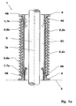
- Fig. 1a shows a conventional gas-insulated dielectric bushing 1, in particular a high voltage bushing 1 for a high voltage electrical apparatus.
- the bushing 1 comprises an insulator part 2; 2a, 2b with a first ground-side mounting flange 4 for mounting the bushing 1 on a grounded housing 5 of an electrical apparatus (not shown) and a second voltage-side mounting flange 8 for mounting the bushing 1 to a high voltage part (not shown).
- the insulator part 2; 2a, 2b has a gas space 20 for an insulating gas 20 in the interior.
- the gas space 20 contains a dielectrically insulating gas 20, e.g. As air, compressed air, nitrogen, SF 6 or similar gas.
- the gas-insulated bushing 1 is thus hollow, typically hollow cylindrical, with an axis 3a, for receiving an electrical part 3 or at least one electrical conductor 3 in the gas space 20.
- the bushing 1 is usually used to connect the encapsulated electrical apparatus to ground potential 5 at High or medium voltage network.
- an internal shielding electrode 6, 6a is necessarily present in order to achieve field relief in the field-loaded zone 7, 7a at the lower ground flange 4 and to reduce or avoid partial discharges and flashovers.
- the shielding electrode 6, 6a is typically in electrical contact 46 with the ground flange 4. It protrudes into the gas space 20 and tapers generally conically upwards.
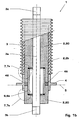
- Fig. 1b shows an example of a solid-state implementation 1 according to the prior art.
- the insulator part 2, 2b is designed as a resin body 2 filled in its entirety with an optional shield 2b.
- the insulator part 2, 2b thus has an insulation space for a solid insulating material 20 in the interior.
- 3b and 3c denote the power connections.
- the insulator part 2, 2b surrounds the current conductor 3.
- a shielding electrode 6, 6a in the field loading zone 7, 7a on the earth flange 4 is present and is electrically conductively connected thereto via a contact 46.
- Fig. 2a-2d and Fig. 3a-3b show exemplary embodiments of a gas-insulated or solid-insulated or otherwise insulated dielectric bushing 1 ', in accordance with the invention at least one shielding electrode 6; 6a, 6b has been omitted without sacrificing dielectric strength or reliability.
- the shielding electrode 6; 6a, 6b is namely for the purpose of field control in the field loading zone 7; 7a, 7b a nonlinear electrical and / or dielectric field control element 9; 9a, 9b; 9i, 9o; 9s on the insulator part 2; 2a, 2b; 2c in the region of the first mounting flange 4 available.
- the field control element 9; 9a, 9b; 9i, 9o; 9s is used instead of the earlier in the insulator part 2; 2a, 2b; 2c arranged shielding electrode 6; 6a, 6b for the dielectric discharge of the field loading zone 7; 7a, 7b.
- the field control element 9; 9a, 9b; 9i, 9o; 9s is used instead of the earlier in the insulator part 2; 2a, 2b; 2c arranged shielding electrode 6; 6a, 6b for the dielectric discharge of the field loading zone 7; 7a, 7b.
- the field control element 9 is designed for the purpose of relieving the field loading zone 7 in such a way that the flange region 7 is stress-relieved.
- the field control element 9 in an intermediate layer 22 between the GRP pipe (glass fiber reinforced plastic and in particular epoxy tube) 2a and the silicone shield 2b in the form of a cylinder jacket-shaped coating 9 is arranged.
- the field control element 9 may be replaced by any known manufacturing or processing process, e.g. B. casting, spraying, winding, extrusion o. ⁇ ., Be applied to the outside of the GRP pipe 2 a.
- the field control element 9; 9a, 9b; 9i, 9o; 9s on: nonlinear electrical varistor characteristics and in particular a critical field strength, the varistor switching behavior of the field control element 9; 9a, 9b; 9i, 9o; 9s characterized; and / or a high dielectric constant ⁇ , in particular ⁇ > 30, preferably ⁇ > 40 and particularly preferably ⁇ > 50.
- the field control element 9 is in electrical contact with the first mounting flange 4 and extends over a predeterminable length l along a longitudinal extension x of the insulator part 2; 2a, 2b. It has a predeterminable thickness d or thickness distribution d (l) as a function of the length l. Preferably, its length l is greater than or equal to a ratio of a maximum test voltage to be tested, in particular a lightning impulse, to the critical electric field strength. This design consideration applies with advantage for all embodiments where the shielding electrode 6a in the Erdflansch Scheme 7a by the field control element 9; 9a; 9i, 9o is replaced.
- Fig. 2b is the field control material 9, 9i disposed on an inner side 21 of the GRP pipe 2a and can additionally help to reduce surface charges there.
- the length l 1 is chosen here by way of example so that the field control layer 9, 9i is not in electrical contact with the counter flange 8.
- Fig. 2c can in addition to the field control 9; 9a another field control element 9; 9b, which likewise has suitable nonlinear electrical and / or dielectric properties, in particular those as previously described for the field control element 9; 9a, and in addition in a field loading zone 7, 7b in the region of the second mounting flange 8 over a predetermined length l; l 2 and thickness d or d (l 2 ) on the insulator part 2; 2a, 2b is present.
- the further field control element 9 is used; 9b as a replacement for a shielding electrode 6b in the region of the second, here the upper, mounting flange 8.
- the field control element 9; 9a including the further field control element 9; 9b is selected in the intermediate layer 22.
- the further field control element 9; 9b in electrical contact with the second mounting flange 8 and / or is the further field control element 9; 9b by a field control material-free zone extending along the longitudinal extent of the insulator part 2; 2a, 2b extends from the field control element 9; 9a separated in the region of the first mounting flange 4.
- a first field control element 9; 9o in the intermediate layer 22 between the GRP pipe 2a and shield 2b and a second field control element 9, 9i on the inner side 21 of the GRP pipe 2a in the Erdflansch Scheme 7a be present.
- the first integrated and the second internal field control element 9o, 9i can be made of the same or other field control material and in particular varistor material.
- the associated thicknesses d o , d i and lengths l o , l i can be designed individually. By way of example, d i > d o and l i ⁇ l o are selected.
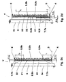
- Fig. 3a and Fig. 3b show an insulator part 2, 2c of a porcelain hollow insulator 2c, which is equipped on the inner side 21 with the field control layer 9, 9i.
- a field control material coating 9o, z. B. in disjoint horizontal Strip 9o preferably between insulator screens 2c and in particular in the lower Erdflansch Scheme 7a, be present.
- the field control material 9; 9a, 9b; 9i, 9o be present in a coating or solid shape on an inner side 21 and / or integrated in an intermediate layer 22 between components 2a, 2b of the insulator part 2; 2a, 2b and / or on an outer side 23 of the insulator part 2; 2a, 2b; 2c is arranged.
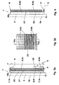
- Fig. 4 takes over the field control material 9; 9s a mechanically supporting function.
- the field control material 9; 9s in the insulator part 2; 2b the exclusive mechanical self-supporting function, so that a conventional self-supporting plastic pipe 2a can be omitted.
- Such a field control material insulator tube 2; 2b including 9s is particularly simple in construction and very thin in diameter.
- Fig. 3a and Fig. 4 on the insulator part 2; 2a, 2b; 2c over the entire surface and along a longitudinal extension x of the insulator part 2; 2a, 2b; 2c continuously and both with the first mounting flange 4; 8 as well as with the second mounting flange 8; 4 are in electrical contact.
- a preferred choice of material for the field control materials 9; 9a, 9b; 9i, 9o; 9s comprises a matrix filled with microvaristor particles and / or high dielectric constant particles.
- Suitable microvaristor particles are, for example, doped ZnO particles, TiO 2 particles or SnO 2 particles. High dielectric constant have z.
- the matrix is chosen application-specific and can, for. Example, an epoxy, silicone, EPDM, thermoplastic, thermoplastic elastomer or glass.
- the filling of the matrix with microvaristor particles may be, for example, between 20% by volume and 60% by volume.
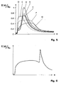
- Fig. 5 12 shows calculations of the E field distribution E (x) normalized to a maximum E field E 0 as a function of the longitudinal coordinate x of the insulator part 2 and the time represented by successive snapshots a, b, c for a conventional feedthrough 1 with shielding electrode 6 according to Fig. 1 and D, E, F, G for an inventive implementation 1 '.
- the calculations were made for a SF 6 170 kV bushing with GRP pipe 2a and silicone shield 2b according to conventional structure 1 or inventive construction 1 '.
- Fig. 5 12 shows calculations of the E field distribution E (x) normalized to a maximum E field E 0 as a function of the longitudinal coordinate x of the insulator part 2 and the time represented by successive snapshots a, b, c for a conventional feedthrough 1 with shielding electrode 6 according to Fig. 1 and D, E, F, G for an inventive implementation 1 '.
- the calculations were made for a SF 6 170 kV bushing with GRP
- the electric field strength E (x) at the silicon - air interface is shown during or shortly after the application of a lightning impulse with time delays of 0.5 ⁇ s / 2.2 ⁇ s / 20 ⁇ s for the curves a, b, c and 0.5 ⁇ s / 1.0 ⁇ s / 5 ⁇ s / 20 ⁇ s for the curves D, E, F, G. It can be clearly seen that the new design of the bushing 1 'avoids the E-field peaks and at any time produces a more homogeneous electric field. Field distribution is achieved. In addition, the areas of increased field strength are no longer stationary, which has an advantageous effect on the dielectric behavior of the bushing 1 '. With the help of the field calculations and the nonlinear electrical and / or dielectric properties of the field control element 9; 9a, 9b; 9i, 9o; 9s, the field control design of the implementation 1 'can be optimized.
- Fig. 6 shows an insufficient design, wherein the field control element 9; 9a, 9b; 9i, 9o; 9s has too high electrical conductivity or the length l; l 1 , l 2 is too short.
- the E-field propagates along the field control layer 9; 9a, 9b; 9i, 9o; 9s, but is not degraded, so that at the end of the field control layer 9; 9a, 9b; 9i, 9o; 9s nevertheless again a field exaggeration occurs, the partial discharges, rollovers or punches.
- too low electrical conductivity of the field control material 9; 9a, 9b; 9i, 9o; 9s the E-field can not be effectively controlled or controlled.
- the simple but effective rule can be stated that the field control element length l; l 1 , l 2 is greater than or equal to choose a ratio of a surge voltage to the critical electric field strength, the varistor switching behavior of the field control element 9; 9a, 9b; 9i, 9o; 9s characterized.
- a high-voltage electrical apparatus in particular a disconnector, outdoor circuit breaker, vacuum switch, dead tank breaker, current transformer, voltage transformer, transformer, power capacitor or cable termination or in an electrical switchgear for high - or medium voltage.
- the invention also relates to a high-voltage electrical apparatus, in particular a disconnector, outdoor circuit breaker, dead tank breaker, current transformer, voltage transformer, transformer, power capacitor or cable termination, in which a dielectric feedthrough 1 'is present as described above.
- an electrical switchgear in particular a high or medium voltage switchgear comprising such a high voltage electrical apparatus claimed.
Claims (13)
- Traversée diélectrique (1'), en particulier traversée à haute tension (1') pour appareil électrique à haute tension, comprenant une partie isolante (2; 2a, 2b; 2c) dotée d'une première bride de montage (4) et d'une deuxième bride de montage (8) permettant de monter le passage (1'),
caractérisé en ce quea) une électrode de blindage (6; 6a, 6b), nécessaire pour un niveau de tension souhaité, est supprimée à l'intérieur du passage (1'), dans une zone (7; 7a, 7b) sollicitée par le champ et située au niveau de la première bride de montage (4; 8),b) au lieu de cette électrode de blindage, pour contrôler le champ dans la zone (7; 7a, 7b) sollicitée par le champ, un élément électriquement linéaire et/ou un élément diélectrique (9; 9a, 9b; 9i, 9o; 9s) sont prévus sur la partie isolante (2; 2a, 2b; 2c) au niveau de la première bride de montage (4) etc) l'élément (9; 9a, 9b; 9i, 9o; 9s) de contrôle du champ est en contact électrique avec la première bride de montage (4). - Passage (1') selon la revendication 1, caractérisé en ce que les propriétés électriques non linéaires et/ou les propriétés diélectriques, la configuration géométrique et l'agencement sur la partie isolante (2; 2a, 2b; 2c) de l'élément (9; 9a, 9b; 9i, 9o; 9s) de commande du champ sont conçus pour délester diélectriquement la zone (7; 7a, 7b) sollicitée par le champ et ce sans électrode de blindage (6; 6a, 6b) pour tous les états de fonctionnement et en particulier pour les pics de tension.
- Passage (1') selon l'une des revendications précédentes, caractérisé en ce que l'élément (9; 9a, 9b; 9i, 9o; 9s) de contrôle du champ présente :a) les propriétés électriques non linéaires d'un varistor et en particulier une intensité critique de champ qui caractérise un comportement de commutation de varistor de l'élément (9; 9a, 9b; 9i, 9o; 9s) de contrôle du champ et/oub) une haute constante diélectrique ε, en particulier ε > 30, de préférence ε > 40 et de façon particulièrement préférable ε > 50.
- Passage (1') selon l'une des revendications précédentes, caractérisé en ce que l'élément (9; 9a, 9b; 9i, 9o; 9s) de contrôle du champ s'étend sur une longueur prédéterminée (l; l1, l2) sur l'extension longitudinale (x) de la partie isolante (2; 2a, 2b; 2c) et présente une épaisseur prédéterminée (d) ou une répartition d'épaisseur (d(l)) qui est fonction de la longueur (l; l1, l2).
- Passage (1') selon la revendication 3, caractéristique a et la revendication 4, caractérisé en ce que la longueur (1; l1, l2) est supérieure ou égale au rapport entre le pic de tension maximum à tester et l'intensité électrique critique.
- Passage (1') selon la revendication 3, caractéristique a ou la revendication 4 dans la mesure où elle dépend de la revendication 3, caractéristique a 4, caractérisé en ce que pour les applications en courant continu, l'élément (9; 9i, 9s) de contrôle du champ est prévu sur toute la surface de la partie isolante (2; 2a, 2b; 2c), est continu le long de l'extension longitudinale (x) de la partie isolante (2; 2a, 2b; 2c) et est en contact électrique à la fois avec la première bride de montage (4) et avec la deuxième bride de montage (8).
- Passage (1') selon l'une des revendications précédentes, caractérisé en ce quea) la première bride de montage (4) est une bride de montage (4) côté terre destinée à monter le passage (1') sur le boîtier (5) raccordé à la terre d'un appareil électrique,b) la deuxième bride de montage (8) est une bride de montage (8) côté tension destinée à monter le passage (1') sur une partie à haute tension et/ouc) la partie isolante (2; 2a, 2b; 2c) présente à l'intérieur un espace d'isolation pour un matériau isolant solide (20) ou pour un isolant liquide (20), ou un espace de gaz pour un gaz isolant (20).
- Passage (1') selon la revendication 7, caractéristique a et la revendication 7, caractéristique b, caractérisé en ce quea) un autre élément (9; 9b) de contrôle du champ est prévu et présente des propriétés électriques non linéaires et/ou des propriétés diélectriques appropriées, en particulier celles définies dans la revendication 3, et est disposé dans une zone (7; 7a, 7b) de sollicitation par le champ au niveau de la deuxième bride de montage (8), sur une longueur prédéterminée (1; l2) et une épaisseur (d, d(l2)) sur la partie isolante (2; 2a, 2b; 2c) etb) en particulier le deuxième élément (9; 9b) de contrôle du champ sert à remplacer une électrode de blindage (6b) au niveau de la deuxième bride de montage (8).
- Passage (1') selon la revendication 8, caractérisé en ce que :a) l'autre élément (9; 9b) de contrôle du champ est en contact électrique avec la deuxième bride de montage (8; 4) et/oub) l'autre élément (9; 9b) de contrôle du champ est séparé de l'élément (9; 9a; 9i, 9o) de contrôle du champ au niveau de la première bride de montage (4) par une zone exempte de matériau de contrôle du champ, qui s'étend le long de l'extension longitudinale de la partie isolante (2; 2a, 2b).
- Passage (1') selon l'une des revendications précédentes, caractérisé en ce quea) l'élément (9; 9a, 9b; 9i, 9o; 9s) de contrôle du champ est prévu sous la forme d'un revêtement ou sous forme massive et est intégré sur un côté intérieur (21) et/ou dans une couche intermédiaire (22) entre les composants (2a, 2b) de la partie isolante (2; 2a, 2b), et/ou est prévu sur un côté extérieur (23), en particulier sous la forme de bandes horizontales (9o) disjointes, de la partie isolante (2; 2a, 2b; 2c), et/ou en ce queb) l'élément (9; 9a, 9b; 9i, 9o; 9s) de contrôle du champ assure une fonction de support mécanique et en particulier le matériau (9; 9a, 9b; 9i, 9o; 9s) de contrôle du champ assure la fonction d'auto-support exclusivement mécanique dans la partie isolante (2; 2a, 2b; 2c).
- Passage (1') selon l'une des revendications précédentes, caractérisé en ce que l'élément (9; 9a, 9b; 9i, 9o; 9s) de contrôle du champ comporte une matrice, en particulier un époxy, un silicone, un EPDM, un thermoplastique, un élastomère thermoplastique ou du verre, et en ce que la matrice est remplie de :a) particules de microvaristor, en particulier des particules dopées de ZnO, de TiO2 ou de SnO2 et/oub) est remplie de particules à haute constante diélectrique, en particulier de particules de BaTiO3 ou de particules de TiO2.
- Appareil électrique à haute tension, en particulier disjoncteur, commutateur de puissance à l'air libre, commutateur sous vide, rupteur à cuve morte, convertisseur de courant, convertisseur de tension, transformateur, condensateur de puissance ou borne de fin de câble, caractérisé en ce qu'il présente un passage diélectrique (1') selon l'une des revendications précédentes.
- Installation de commutation électrique, en particulier installation de commutation électrique à haute ou moyenne tension, caractérisée par un appareil électrique à haute tension selon la revendication 12.
Priority Applications (3)
| Application Number | Priority Date | Filing Date | Title |
|---|---|---|---|
| AT04405151T ATE546818T1 (de) | 2004-03-15 | 2004-03-15 | Hochspannungsdurchführung mit feldsteuermaterial |
| EP04405151A EP1577904B1 (fr) | 2004-03-15 | 2004-03-15 | Traversée haute tension avec élément pour les contrôle du champ électrique |
| US11/079,858 US7262367B2 (en) | 2004-03-15 | 2005-03-15 | High voltage bushing with field control material |
Applications Claiming Priority (1)
| Application Number | Priority Date | Filing Date | Title |
|---|---|---|---|
| EP04405151A EP1577904B1 (fr) | 2004-03-15 | 2004-03-15 | Traversée haute tension avec élément pour les contrôle du champ électrique |
Publications (2)
| Publication Number | Publication Date |
|---|---|
| EP1577904A1 EP1577904A1 (fr) | 2005-09-21 |
| EP1577904B1 true EP1577904B1 (fr) | 2012-02-22 |
Family
ID=34833824
Family Applications (1)
| Application Number | Title | Priority Date | Filing Date |
|---|---|---|---|
| EP04405151A Expired - Lifetime EP1577904B1 (fr) | 2004-03-15 | 2004-03-15 | Traversée haute tension avec élément pour les contrôle du champ électrique |
Country Status (3)
| Country | Link |
|---|---|
| US (1) | US7262367B2 (fr) |
| EP (1) | EP1577904B1 (fr) |
| AT (1) | ATE546818T1 (fr) |
Cited By (1)
| Publication number | Priority date | Publication date | Assignee | Title |
|---|---|---|---|---|
| CN106199117A (zh) * | 2016-07-15 | 2016-12-07 | 中国南方电网有限责任公司超高压输电公司检修试验中心 | 一种直流分压器辅助伞裙设计方法 |
Families Citing this family (43)
| Publication number | Priority date | Publication date | Assignee | Title |
|---|---|---|---|---|
| SE526713C2 (sv) * | 2003-07-11 | 2005-10-25 | Abb Research Ltd | Genomföring samt förfarande för tillverkning av genomföringen |
| EP1736998A1 (fr) * | 2005-06-21 | 2006-12-27 | Abb Research Ltd. | Bande à la propriété de varistor pour le contrôle d'un champ électrique |
| EP1811626B1 (fr) * | 2006-01-24 | 2016-04-13 | Nexans | Traversée électrique |
| DE102006038221B4 (de) * | 2006-08-03 | 2009-03-26 | Siemens Ag | Vorrichtung zur elektrischen Abschirmung einer Hochspannungsdurchführung |
| CN101506911B (zh) * | 2006-08-31 | 2011-04-06 | Abb技术有限公司 | 高压套管 |
| CN101136270B (zh) * | 2006-08-31 | 2013-03-20 | Abb技术有限公司 | 高压套管及其制造方法以及高压设备 |
| US20080157783A1 (en) * | 2007-01-01 | 2008-07-03 | Maxwell Technologies, Inc. | Apparatus and method for monitoring high voltage capacitors |
| SE531321C2 (sv) * | 2007-07-05 | 2009-02-24 | Abb Technology Ag | Högspänningskabelanslutning |
| DE102007033705B4 (de) * | 2007-07-17 | 2009-03-05 | Siemens Ag | Wandleranordnung einer metallgekapselten, gasisolierten Schaltanlage sowie metallgekapselte, gasisolierte Schaltanlage |
| EP2039496A1 (fr) * | 2007-09-20 | 2009-03-25 | ABB Research Ltd. | Procédé de fabrication d'un produit en caoutchouc |
| EP2053616A1 (fr) * | 2007-10-26 | 2009-04-29 | ABB Research Ltd. | Garniture d'étanchéité d'extérieur haute tension |
| US7807930B1 (en) * | 2007-11-30 | 2010-10-05 | The United States Of America As Represented By The Secretary Of The Navy | High-voltage feed-through bushing with internal and external electric field grading elements |
| DE102008009333A1 (de) | 2008-02-14 | 2009-08-20 | Lapp Insulator Gmbh & Co. Kg | Feldgesteuerter Verbundisolator |
| EP2154700A1 (fr) * | 2008-08-14 | 2010-02-17 | ABB Technology AG | Isolant haute tension doté d'un élément de commande de champ |
| EP2276041B1 (fr) * | 2009-07-15 | 2013-09-25 | ABB Research Ltd. | Dispositif de connexion électrique et installation électrique |
| CN101714446A (zh) * | 2009-09-10 | 2010-05-26 | 北京天威瑞恒高压套管有限公司 | 玻璃钢电容式多芯变压器套管 |
| CA2811262C (fr) | 2009-09-14 | 2016-06-21 | Roger Faulkner | Systeme modulaire de transmission souterraine de courant electrique continu a haute tension |
| US8525526B2 (en) * | 2009-11-13 | 2013-09-03 | Hubbell Incorporated | High voltage test terminal having a shock-absorbing insulator |
| EP2375423A1 (fr) * | 2010-04-07 | 2011-10-12 | ABB Research Ltd. | Traversée électrique |
| EP2922164A1 (fr) | 2010-05-21 | 2015-09-23 | ABB Research Ltd. | Terminaison d'un câble haute tension à courant continu |
| CN102906953B (zh) | 2010-05-21 | 2016-04-13 | Abb研究有限公司 | 高压直流电缆终端设备 |
| EP2572422A2 (fr) | 2010-05-21 | 2013-03-27 | ABB Research Ltd. | Appareil de terminaison de câble pour courant continu à haute tension |
| CN102906955B (zh) | 2010-05-21 | 2015-09-23 | Abb研究有限公司 | 高压直流电缆终端装置 |
| EP2431982B1 (fr) * | 2010-09-21 | 2014-11-26 | ABB Technology AG | Ligne enfichable et installation haute tension dotée d'une telle ligne |
| DE102010043995A1 (de) * | 2010-11-16 | 2012-05-16 | Siemens Aktiengesellschaft | Isolatoranordnung sowie Verfahren zur Herstellung einer Isolatoranordnung |
| DE102010043990A1 (de) * | 2010-11-16 | 2012-05-16 | Siemens Aktiengesellschaft | Isolatoranordnung sowie Verfahren zur Herstellung einer Isolatoranordnung |
| EP2482290B1 (fr) * | 2011-01-28 | 2017-07-19 | ABB Schweiz AG | Design de traversée à température compensée |
| RU2457564C1 (ru) * | 2011-02-21 | 2012-07-27 | Российская Федерация, от имени которой выступает Государственная корпорация по атомной энергии "Росатом" (Госкорпорация "Росатом") | Переход высоковольтный |
| US8704097B2 (en) * | 2012-01-23 | 2014-04-22 | General Electric Company | High voltage bushing assembly |
| US8716601B2 (en) | 2012-02-08 | 2014-05-06 | General Electric Company | Corona resistant high voltage bushing assembly |
| DE102012104137A1 (de) * | 2012-05-11 | 2013-11-14 | Maschinenfabrik Reinhausen Gmbh | Feldgesteuerter Verbundisolator |
| US9078346B2 (en) * | 2013-03-11 | 2015-07-07 | Varian Semiconductor Equipment Associates, Inc. | Insulator protection |
| DE102013204706A1 (de) * | 2013-03-18 | 2014-09-18 | Siemens Aktiengesellschaft | Widerstandsbelag für ein Gleichstromisoliersystem |
| DE102014004284B4 (de) * | 2014-03-26 | 2019-11-14 | Lapp Insulators Gmbh | Hochspannungsdurchführung |
| CN103971861A (zh) * | 2014-05-21 | 2014-08-06 | 北京铁道工程机电技术研究所有限公司 | 一种具有防界面击穿的动车车顶复合绝缘子 |
| EP3278911B1 (fr) * | 2015-03-30 | 2020-04-15 | Mitsubishi Hitachi Tool Engineering, Ltd. | Mèche |
| EP3096334B1 (fr) * | 2015-05-22 | 2020-12-30 | ABB Power Grids Switzerland AG | Traversée électrique |
| DE102017212977A1 (de) * | 2017-07-27 | 2019-01-31 | Siemens Aktiengesellschaft | Steckbare Hochspannungsdurchführung und elektrisches Gerät mit der steckbaren Hochspannungsdurchführung |
| CN107800109A (zh) * | 2017-10-31 | 2018-03-13 | 清华大学 | 采用非线性电导材料预制橡胶压控管的电缆端头 |
| EP3591672B1 (fr) * | 2018-07-02 | 2023-03-29 | Hitachi Energy Switzerland AG | Isolant a gradient de résistivité |
| EP3667684A1 (fr) * | 2018-12-12 | 2020-06-17 | ABB Schweiz AG | Traversée électrique |
| CN113450948A (zh) * | 2021-07-19 | 2021-09-28 | 上海甲希科技有限公司 | 一种绝缘管型母线及绝缘管型母线的绝缘制造方法和设备 |
| DE102022206149A1 (de) * | 2022-06-21 | 2023-12-21 | Siemens Energy Global GmbH & Co. KG | Durchführungsisolator |
Family Cites Families (13)
| Publication number | Priority date | Publication date | Assignee | Title |
|---|---|---|---|---|
| US1484051A (en) * | 1919-04-10 | 1924-02-19 | Ohio Brass Co | Insulator |
| GB842039A (en) * | 1957-04-06 | 1960-07-20 | Asea Ab | High voltage devices comprising a potential gradient equalizing coating |
| FR1378902A (fr) * | 1963-08-20 | 1964-11-20 | Comp Generale Electricite | Procédé de fabrication d'un barreau d'ancrage à haute résistance mécanique et électrique et barreau ainsi obtenu |
| US3318995A (en) | 1966-04-25 | 1967-05-09 | Westinghouse Electric Corp | Cast electrical bushing construction having controlled and shielded shrinkage voids |
| FR2198231B1 (fr) * | 1972-09-04 | 1980-02-22 | Ceraver | |
| SE429907B (sv) * | 1978-09-13 | 1983-10-03 | Asea Ab | Elektrisk hogspenningsgenomforing for ett metallkapslat, tryckgasisolerat stellverk |
| US4905118A (en) * | 1988-03-31 | 1990-02-27 | Hubbell Incorporated | Base mounted electrical assembly |
| US5214249A (en) * | 1991-02-22 | 1993-05-25 | Hubbell Incorporated | Electrical assembly with end collars for coupling ends of a weathershed housing to the end fittings |
| SE9704824D0 (sv) * | 1997-12-22 | 1997-12-22 | Asea Brown Boveri | Fiberkompositföremål och metod för att framställa sådant fiberkompositföremål |
| DE19844409C2 (de) | 1998-09-28 | 2000-12-21 | Hochspannungsgeraete Porz Gmbh | Hochspannungs-Durchführung |
| DE19856123C2 (de) * | 1998-12-04 | 2000-12-07 | Siemens Ag | Hohlisolator |
| GB0103255D0 (en) * | 2001-02-09 | 2001-03-28 | Tyco Electronics Raychem Gmbh | Insulator arrangement |
| US6441310B1 (en) * | 2001-03-30 | 2002-08-27 | Hubbell Incorporated | Moisture activated barrier for electrical assemblies |
-
2004
- 2004-03-15 AT AT04405151T patent/ATE546818T1/de active
- 2004-03-15 EP EP04405151A patent/EP1577904B1/fr not_active Expired - Lifetime
-
2005
- 2005-03-15 US US11/079,858 patent/US7262367B2/en active Active
Cited By (2)
| Publication number | Priority date | Publication date | Assignee | Title |
|---|---|---|---|---|
| CN106199117A (zh) * | 2016-07-15 | 2016-12-07 | 中国南方电网有限责任公司超高压输电公司检修试验中心 | 一种直流分压器辅助伞裙设计方法 |
| CN106199117B (zh) * | 2016-07-15 | 2018-11-23 | 中国南方电网有限责任公司超高压输电公司检修试验中心 | 一种直流分压器辅助伞裙设计方法 |
Also Published As
| Publication number | Publication date |
|---|---|
| US7262367B2 (en) | 2007-08-28 |
| ATE546818T1 (de) | 2012-03-15 |
| EP1577904A1 (fr) | 2005-09-21 |
| US20050199418A1 (en) | 2005-09-15 |
Similar Documents
| Publication | Publication Date | Title |
|---|---|---|
| EP1577904B1 (fr) | Traversée haute tension avec élément pour les contrôle du champ électrique | |
| EP1254497B1 (fr) | Boite d'extremite de cable | |
| EP2702597B1 (fr) | Coupe-circuit de surtension | |
| EP3807920B1 (fr) | Tube de commutation sous vide et dispositif de commutation à haute tension | |
| EP1569255B1 (fr) | Interrupteur de mise à la terre compact pour Disjoncteurs à isolation par gas | |
| DE2934805C2 (de) | Elektrische Hochspannungsdurchführung | |
| EP3472847A1 (fr) | Ensemble d'isolation pour une installation de commutation de hautes ou moyennes tensions | |
| DE19500849A1 (de) | Elektrisches Bauteil | |
| EP1603141B1 (fr) | Limiteur de surtensions avec isolation au gaz | |
| EP2715743A1 (fr) | Composant électrique pour installation haute tension | |
| WO2022069197A1 (fr) | Conducteur revêtu dans un appareil à haute tension et procédé pour augmenter la résistance diélectrique | |
| WO2017012740A1 (fr) | Composant de la technique énergétique, en particulier tube commutateur à vide | |
| DE2912844A1 (de) | Blitzschutzvorrichtung | |
| EP4007924B1 (fr) | Appareillage de mesure pour mesurer un potentiel de tension sur un conducteur dans un dispositif de commutation de puissance et dispositif de commutation de puissance correspondant | |
| DE102011006013B3 (de) | Vakuumschaltröhre und Schalterpol | |
| DE102005060908A1 (de) | Elektrisches Schaltgerät, insbesondere Hochspannungs-Leistungsschalter, mit einem Gehäuse | |
| DE102021207962A1 (de) | Vakuumschaltröhre und Anordnung mit Vakuumschaltröhren sowie Verfahren zum Absteuern von Vakuumschaltröhren | |
| WO2023147967A1 (fr) | Ampoule à vide commandable, et agencement et procédé de commande d'ampoules à vide | |
| EP4244879A1 (fr) | Dispositif de commutation électrique pour utilisations à moyenne et/ou haute tension | |
| DE102021207963A1 (de) | Vakuumschaltröhre zum Schalten von Spannungen | |
| DD241809A1 (de) | Isoliergehaeuse fuer eine vakuumschaltkammer | |
| WO1994006135A1 (fr) | Transformateur de courant | |
| WO2001041273A1 (fr) | Isolateurs et transformateurs d'intensite de traversee destines a des circuits moyenne tension isoles par air a blindage metallique | |
| DE102021207960A1 (de) | Vakuumschaltröhre und Anordnung mit Vakuumschaltröhren sowie Verfahren zum Absteuern von Vakuumschaltröhren | |
| DE3906553A1 (de) | Abschirmelektrode |
Legal Events
| Date | Code | Title | Description |
|---|---|---|---|
| PUAI | Public reference made under article 153(3) epc to a published international application that has entered the european phase |
Free format text: ORIGINAL CODE: 0009012 |
|
| AK | Designated contracting states |
Kind code of ref document: A1 Designated state(s): AT BE BG CH CY CZ DE DK EE ES FI FR GB GR HU IE IT LI LU MC NL PL PT RO SE SI SK TR |
|
| AX | Request for extension of the european patent |
Extension state: AL LT LV MK |
|
| 17P | Request for examination filed |
Effective date: 20060116 |
|
| AKX | Designation fees paid |
Designated state(s): AT BE BG CH CY CZ DE DK EE ES FI FR GB GR HU IE IT LI LU MC NL PL PT RO SE SI SK TR |
|
| GRAP | Despatch of communication of intention to grant a patent |
Free format text: ORIGINAL CODE: EPIDOSNIGR1 |
|
| GRAS | Grant fee paid |
Free format text: ORIGINAL CODE: EPIDOSNIGR3 |
|
| GRAA | (expected) grant |
Free format text: ORIGINAL CODE: 0009210 |
|
| AK | Designated contracting states |
Kind code of ref document: B1 Designated state(s): AT BE BG CH CY CZ DE DK EE ES FI FR GB GR HU IE IT LI LU MC NL PL PT RO SE SI SK TR |
|
| REG | Reference to a national code |
Ref country code: GB Ref legal event code: FG4D Free format text: NOT ENGLISH |
|
| REG | Reference to a national code |
Ref country code: CH Ref legal event code: EP |
|
| REG | Reference to a national code |
Ref country code: AT Ref legal event code: REF Ref document number: 546818 Country of ref document: AT Kind code of ref document: T Effective date: 20120315 |
|
| REG | Reference to a national code |
Ref country code: IE Ref legal event code: FG4D Free format text: LANGUAGE OF EP DOCUMENT: GERMAN |
|
| REG | Reference to a national code |
Ref country code: DE Ref legal event code: R096 Ref document number: 502004013314 Country of ref document: DE Effective date: 20120419 |
|
| REG | Reference to a national code |
Ref country code: SE Ref legal event code: TRGR |
|
| REG | Reference to a national code |
Ref country code: NL Ref legal event code: VDEP Effective date: 20120222 |
|
| PG25 | Lapsed in a contracting state [announced via postgrant information from national office to epo] |
Ref country code: NL Free format text: LAPSE BECAUSE OF FAILURE TO SUBMIT A TRANSLATION OF THE DESCRIPTION OR TO PAY THE FEE WITHIN THE PRESCRIBED TIME-LIMIT Effective date: 20120222 |
|
| PG25 | Lapsed in a contracting state [announced via postgrant information from national office to epo] |
Ref country code: GR Free format text: LAPSE BECAUSE OF FAILURE TO SUBMIT A TRANSLATION OF THE DESCRIPTION OR TO PAY THE FEE WITHIN THE PRESCRIBED TIME-LIMIT Effective date: 20120523 Ref country code: PT Free format text: LAPSE BECAUSE OF FAILURE TO SUBMIT A TRANSLATION OF THE DESCRIPTION OR TO PAY THE FEE WITHIN THE PRESCRIBED TIME-LIMIT Effective date: 20120622 Ref country code: FI Free format text: LAPSE BECAUSE OF FAILURE TO SUBMIT A TRANSLATION OF THE DESCRIPTION OR TO PAY THE FEE WITHIN THE PRESCRIBED TIME-LIMIT Effective date: 20120222 |
|
| REG | Reference to a national code |
Ref country code: IE Ref legal event code: FD4D |
|
| PG25 | Lapsed in a contracting state [announced via postgrant information from national office to epo] |
Ref country code: CY Free format text: LAPSE BECAUSE OF FAILURE TO SUBMIT A TRANSLATION OF THE DESCRIPTION OR TO PAY THE FEE WITHIN THE PRESCRIBED TIME-LIMIT Effective date: 20120222 |
|
| BERE | Be: lapsed |
Owner name: ABB RESEARCH LTD. Effective date: 20120331 |
|
| PG25 | Lapsed in a contracting state [announced via postgrant information from national office to epo] |
Ref country code: DK Free format text: LAPSE BECAUSE OF FAILURE TO SUBMIT A TRANSLATION OF THE DESCRIPTION OR TO PAY THE FEE WITHIN THE PRESCRIBED TIME-LIMIT Effective date: 20120222 Ref country code: MC Free format text: LAPSE BECAUSE OF NON-PAYMENT OF DUE FEES Effective date: 20120331 Ref country code: IE Free format text: LAPSE BECAUSE OF FAILURE TO SUBMIT A TRANSLATION OF THE DESCRIPTION OR TO PAY THE FEE WITHIN THE PRESCRIBED TIME-LIMIT Effective date: 20120222 Ref country code: EE Free format text: LAPSE BECAUSE OF FAILURE TO SUBMIT A TRANSLATION OF THE DESCRIPTION OR TO PAY THE FEE WITHIN THE PRESCRIBED TIME-LIMIT Effective date: 20120222 Ref country code: CZ Free format text: LAPSE BECAUSE OF FAILURE TO SUBMIT A TRANSLATION OF THE DESCRIPTION OR TO PAY THE FEE WITHIN THE PRESCRIBED TIME-LIMIT Effective date: 20120222 Ref country code: SI Free format text: LAPSE BECAUSE OF FAILURE TO SUBMIT A TRANSLATION OF THE DESCRIPTION OR TO PAY THE FEE WITHIN THE PRESCRIBED TIME-LIMIT Effective date: 20120222 Ref country code: PL Free format text: LAPSE BECAUSE OF FAILURE TO SUBMIT A TRANSLATION OF THE DESCRIPTION OR TO PAY THE FEE WITHIN THE PRESCRIBED TIME-LIMIT Effective date: 20120222 Ref country code: RO Free format text: LAPSE BECAUSE OF FAILURE TO SUBMIT A TRANSLATION OF THE DESCRIPTION OR TO PAY THE FEE WITHIN THE PRESCRIBED TIME-LIMIT Effective date: 20120222 |
|
| PG25 | Lapsed in a contracting state [announced via postgrant information from national office to epo] |
Ref country code: SK Free format text: LAPSE BECAUSE OF FAILURE TO SUBMIT A TRANSLATION OF THE DESCRIPTION OR TO PAY THE FEE WITHIN THE PRESCRIBED TIME-LIMIT Effective date: 20120222 |
|
| PLBE | No opposition filed within time limit |
Free format text: ORIGINAL CODE: 0009261 |
|
| STAA | Information on the status of an ep patent application or granted ep patent |
Free format text: STATUS: NO OPPOSITION FILED WITHIN TIME LIMIT |
|
| 26N | No opposition filed |
Effective date: 20121123 |
|
| GBPC | Gb: european patent ceased through non-payment of renewal fee |
Effective date: 20120522 |
|
| PG25 | Lapsed in a contracting state [announced via postgrant information from national office to epo] |
Ref country code: BE Free format text: LAPSE BECAUSE OF NON-PAYMENT OF DUE FEES Effective date: 20120331 |
|
| REG | Reference to a national code |
Ref country code: DE Ref legal event code: R097 Ref document number: 502004013314 Country of ref document: DE Effective date: 20121123 |
|
| PG25 | Lapsed in a contracting state [announced via postgrant information from national office to epo] |
Ref country code: GB Free format text: LAPSE BECAUSE OF NON-PAYMENT OF DUE FEES Effective date: 20120522 Ref country code: ES Free format text: LAPSE BECAUSE OF FAILURE TO SUBMIT A TRANSLATION OF THE DESCRIPTION OR TO PAY THE FEE WITHIN THE PRESCRIBED TIME-LIMIT Effective date: 20120602 |
|
| REG | Reference to a national code |
Ref country code: AT Ref legal event code: MM01 Ref document number: 546818 Country of ref document: AT Kind code of ref document: T Effective date: 20120315 |
|
| PG25 | Lapsed in a contracting state [announced via postgrant information from national office to epo] |
Ref country code: AT Free format text: LAPSE BECAUSE OF NON-PAYMENT OF DUE FEES Effective date: 20120315 Ref country code: BG Free format text: LAPSE BECAUSE OF FAILURE TO SUBMIT A TRANSLATION OF THE DESCRIPTION OR TO PAY THE FEE WITHIN THE PRESCRIBED TIME-LIMIT Effective date: 20120522 |
|
| PG25 | Lapsed in a contracting state [announced via postgrant information from national office to epo] |
Ref country code: TR Free format text: LAPSE BECAUSE OF FAILURE TO SUBMIT A TRANSLATION OF THE DESCRIPTION OR TO PAY THE FEE WITHIN THE PRESCRIBED TIME-LIMIT Effective date: 20120222 |
|
| PG25 | Lapsed in a contracting state [announced via postgrant information from national office to epo] |
Ref country code: LU Free format text: LAPSE BECAUSE OF NON-PAYMENT OF DUE FEES Effective date: 20120315 |
|
| PG25 | Lapsed in a contracting state [announced via postgrant information from national office to epo] |
Ref country code: HU Free format text: LAPSE BECAUSE OF FAILURE TO SUBMIT A TRANSLATION OF THE DESCRIPTION OR TO PAY THE FEE WITHIN THE PRESCRIBED TIME-LIMIT Effective date: 20040315 |
|
| REG | Reference to a national code |
Ref country code: FR Ref legal event code: PLFP Year of fee payment: 13 |
|
| REG | Reference to a national code |
Ref country code: FR Ref legal event code: PLFP Year of fee payment: 14 |
|
| REG | Reference to a national code |
Ref country code: FR Ref legal event code: PLFP Year of fee payment: 15 |
|
| REG | Reference to a national code |
Ref country code: CH Ref legal event code: PFUS Owner name: ABB SCHWEIZ AG, CH Free format text: FORMER OWNER: ABB RESEARCH LTD., CH |
|
| REG | Reference to a national code |
Ref country code: DE Ref legal event code: R081 Ref document number: 502004013314 Country of ref document: DE Owner name: HITACHI ENERGY SWITZERLAND AG, CH Free format text: FORMER OWNER: ABB RESEARCH LTD., 8050 ZUERICH, CH Ref country code: DE Ref legal event code: R082 Ref document number: 502004013314 Country of ref document: DE Representative=s name: ZIMMERMANN & PARTNER PATENTANWAELTE MBB, DE Ref country code: DE Ref legal event code: R081 Ref document number: 502004013314 Country of ref document: DE Owner name: ABB SCHWEIZ AG, CH Free format text: FORMER OWNER: ABB RESEARCH LTD., 8050 ZUERICH, CH Ref country code: DE Ref legal event code: R081 Ref document number: 502004013314 Country of ref document: DE Owner name: ABB POWER GRIDS SWITZERLAND AG, CH Free format text: FORMER OWNER: ABB RESEARCH LTD., 8050 ZUERICH, CH Ref country code: DE Ref legal event code: R082 Ref document number: 502004013314 Country of ref document: DE Representative=s name: DENNEMEYER & ASSOCIATES S.A., DE |
|
| REG | Reference to a national code |
Ref country code: CH Ref legal event code: PUE Owner name: ABB POWER GRIDS SWITZERLAND AG, CH Free format text: FORMER OWNER: ABB SCHWEIZ AG, CH |
|
| REG | Reference to a national code |
Ref country code: DE Ref legal event code: R081 Ref document number: 502004013314 Country of ref document: DE Owner name: HITACHI ENERGY SWITZERLAND AG, CH Free format text: FORMER OWNER: ABB SCHWEIZ AG, BADEN, CH Ref country code: DE Ref legal event code: R082 Ref document number: 502004013314 Country of ref document: DE Representative=s name: DENNEMEYER & ASSOCIATES S.A., DE Ref country code: DE Ref legal event code: R081 Ref document number: 502004013314 Country of ref document: DE Owner name: ABB POWER GRIDS SWITZERLAND AG, CH Free format text: FORMER OWNER: ABB SCHWEIZ AG, BADEN, CH |
|
| PGFP | Annual fee paid to national office [announced via postgrant information from national office to epo] |
Ref country code: CH Payment date: 20220321 Year of fee payment: 19 |
|
| PGFP | Annual fee paid to national office [announced via postgrant information from national office to epo] |
Ref country code: SE Payment date: 20220321 Year of fee payment: 19 Ref country code: IT Payment date: 20220322 Year of fee payment: 19 Ref country code: FR Payment date: 20220322 Year of fee payment: 19 |
|
| REG | Reference to a national code |
Ref country code: DE Ref legal event code: R081 Ref document number: 502004013314 Country of ref document: DE Owner name: HITACHI ENERGY SWITZERLAND AG, CH Free format text: FORMER OWNER: ABB POWER GRIDS SWITZERLAND AG, BADEN, CH |
|
| PGFP | Annual fee paid to national office [announced via postgrant information from national office to epo] |
Ref country code: DE Payment date: 20230321 Year of fee payment: 20 |
|
| P01 | Opt-out of the competence of the unified patent court (upc) registered |
Effective date: 20230527 |
|
| REG | Reference to a national code |
Ref country code: SE Ref legal event code: EUG Ref country code: CH Ref legal event code: PL |
|
| PG25 | Lapsed in a contracting state [announced via postgrant information from national office to epo] |
Ref country code: SE Free format text: LAPSE BECAUSE OF NON-PAYMENT OF DUE FEES Effective date: 20230316 Ref country code: LI Free format text: LAPSE BECAUSE OF NON-PAYMENT OF DUE FEES Effective date: 20230331 Ref country code: FR Free format text: LAPSE BECAUSE OF NON-PAYMENT OF DUE FEES Effective date: 20230331 Ref country code: CH Free format text: LAPSE BECAUSE OF NON-PAYMENT OF DUE FEES Effective date: 20230331 |
|
| REG | Reference to a national code |
Ref country code: DE Ref legal event code: R071 Ref document number: 502004013314 Country of ref document: DE |
|
| PG25 | Lapsed in a contracting state [announced via postgrant information from national office to epo] |
Ref country code: IT Free format text: LAPSE BECAUSE OF NON-PAYMENT OF DUE FEES Effective date: 20230315 |