EP1576649B1 - Stapelbare schichten die eingekapselte integrierte schaltungschips mit einer oder mehreren darüberliegenden verbindungsschichten beinhalten und verfahren zu deren herstellung - Google Patents
Stapelbare schichten die eingekapselte integrierte schaltungschips mit einer oder mehreren darüberliegenden verbindungsschichten beinhalten und verfahren zu deren herstellung Download PDFInfo
- Publication number
- EP1576649B1 EP1576649B1 EP02789292A EP02789292A EP1576649B1 EP 1576649 B1 EP1576649 B1 EP 1576649B1 EP 02789292 A EP02789292 A EP 02789292A EP 02789292 A EP02789292 A EP 02789292A EP 1576649 B1 EP1576649 B1 EP 1576649B1
- Authority
- EP
- European Patent Office
- Prior art keywords
- integrated circuit
- circuit chip
- interconnect assembly
- interconnect
- test pad
- Prior art date
- Legal status (The legal status is an assumption and is not a legal conclusion. Google has not performed a legal analysis and makes no representation as to the accuracy of the status listed.)
- Expired - Lifetime
Links
Images


Classifications
-
- H—ELECTRICITY
- H10—SEMICONDUCTOR DEVICES; ELECTRIC SOLID-STATE DEVICES NOT OTHERWISE PROVIDED FOR
- H10W—GENERIC PACKAGES, INTERCONNECTIONS, CONNECTORS OR OTHER CONSTRUCTIONAL DETAILS OF DEVICES COVERED BY CLASS H10
- H10W74/00—Encapsulations, e.g. protective coatings
- H10W74/01—Manufacture or treatment
- H10W74/019—Manufacture or treatment using temporary auxiliary substrates
-
- H—ELECTRICITY
- H10—SEMICONDUCTOR DEVICES; ELECTRIC SOLID-STATE DEVICES NOT OTHERWISE PROVIDED FOR
- H10P—GENERIC PROCESSES OR APPARATUS FOR THE MANUFACTURE OR TREATMENT OF DEVICES COVERED BY CLASS H10
- H10P72/00—Handling or holding of wafers, substrates or devices during manufacture or treatment thereof
- H10P72/70—Handling or holding of wafers, substrates or devices during manufacture or treatment thereof for supporting or gripping
- H10P72/74—Handling or holding of wafers, substrates or devices during manufacture or treatment thereof for supporting or gripping using temporarily an auxiliary support
-
- H—ELECTRICITY
- H10—SEMICONDUCTOR DEVICES; ELECTRIC SOLID-STATE DEVICES NOT OTHERWISE PROVIDED FOR
- H10P—GENERIC PROCESSES OR APPARATUS FOR THE MANUFACTURE OR TREATMENT OF DEVICES COVERED BY CLASS H10
- H10P74/00—Testing or measuring during manufacture or treatment of wafers, substrates or devices
- H10P74/27—Structural arrangements therefor
- H10P74/273—Interconnections for measuring or testing, e.g. probe pads
-
- H—ELECTRICITY
- H10—SEMICONDUCTOR DEVICES; ELECTRIC SOLID-STATE DEVICES NOT OTHERWISE PROVIDED FOR
- H10W—GENERIC PACKAGES, INTERCONNECTIONS, CONNECTORS OR OTHER CONSTRUCTIONAL DETAILS OF DEVICES COVERED BY CLASS H10
- H10W70/00—Package substrates; Interposers; Redistribution layers [RDL]
- H10W70/60—Insulating or insulated package substrates; Interposers; Redistribution layers
- H10W70/611—Insulating or insulated package substrates; Interposers; Redistribution layers for connecting multiple chips together
-
- H—ELECTRICITY
- H10—SEMICONDUCTOR DEVICES; ELECTRIC SOLID-STATE DEVICES NOT OTHERWISE PROVIDED FOR
- H10W—GENERIC PACKAGES, INTERCONNECTIONS, CONNECTORS OR OTHER CONSTRUCTIONAL DETAILS OF DEVICES COVERED BY CLASS H10
- H10W70/00—Package substrates; Interposers; Redistribution layers [RDL]
- H10W70/60—Insulating or insulated package substrates; Interposers; Redistribution layers
- H10W70/699—Insulating or insulated package substrates; Interposers; Redistribution layers for flat cards, e.g. credit cards
-
- H—ELECTRICITY
- H10—SEMICONDUCTOR DEVICES; ELECTRIC SOLID-STATE DEVICES NOT OTHERWISE PROVIDED FOR
- H10W—GENERIC PACKAGES, INTERCONNECTIONS, CONNECTORS OR OTHER CONSTRUCTIONAL DETAILS OF DEVICES COVERED BY CLASS H10
- H10W74/00—Encapsulations, e.g. protective coatings
- H10W74/10—Encapsulations, e.g. protective coatings characterised by their shape or disposition
- H10W74/111—Encapsulations, e.g. protective coatings characterised by their shape or disposition the semiconductor body being completely enclosed
- H10W74/114—Encapsulations, e.g. protective coatings characterised by their shape or disposition the semiconductor body being completely enclosed by a substrate and the encapsulations
-
- H—ELECTRICITY
- H10—SEMICONDUCTOR DEVICES; ELECTRIC SOLID-STATE DEVICES NOT OTHERWISE PROVIDED FOR
- H10W—GENERIC PACKAGES, INTERCONNECTIONS, CONNECTORS OR OTHER CONSTRUCTIONAL DETAILS OF DEVICES COVERED BY CLASS H10
- H10W90/00—Package configurations
-
- H—ELECTRICITY
- H10—SEMICONDUCTOR DEVICES; ELECTRIC SOLID-STATE DEVICES NOT OTHERWISE PROVIDED FOR
- H10P—GENERIC PROCESSES OR APPARATUS FOR THE MANUFACTURE OR TREATMENT OF DEVICES COVERED BY CLASS H10
- H10P72/00—Handling or holding of wafers, substrates or devices during manufacture or treatment thereof
- H10P72/70—Handling or holding of wafers, substrates or devices during manufacture or treatment thereof for supporting or gripping
- H10P72/74—Handling or holding of wafers, substrates or devices during manufacture or treatment thereof for supporting or gripping using temporarily an auxiliary support
- H10P72/743—Handling or holding of wafers, substrates or devices during manufacture or treatment thereof for supporting or gripping using temporarily an auxiliary support used as a support during manufacture of interconnect decals or build up layers
-
- H—ELECTRICITY
- H10—SEMICONDUCTOR DEVICES; ELECTRIC SOLID-STATE DEVICES NOT OTHERWISE PROVIDED FOR
- H10W—GENERIC PACKAGES, INTERCONNECTIONS, CONNECTORS OR OTHER CONSTRUCTIONAL DETAILS OF DEVICES COVERED BY CLASS H10
- H10W70/00—Package substrates; Interposers; Redistribution layers [RDL]
- H10W70/60—Insulating or insulated package substrates; Interposers; Redistribution layers
-
- H—ELECTRICITY
- H10—SEMICONDUCTOR DEVICES; ELECTRIC SOLID-STATE DEVICES NOT OTHERWISE PROVIDED FOR
- H10W—GENERIC PACKAGES, INTERCONNECTIONS, CONNECTORS OR OTHER CONSTRUCTIONAL DETAILS OF DEVICES COVERED BY CLASS H10
- H10W72/00—Interconnections or connectors in packages
- H10W72/801—Interconnections on sidewalls of containers
-
- H—ELECTRICITY
- H10—SEMICONDUCTOR DEVICES; ELECTRIC SOLID-STATE DEVICES NOT OTHERWISE PROVIDED FOR
- H10W—GENERIC PACKAGES, INTERCONNECTIONS, CONNECTORS OR OTHER CONSTRUCTIONAL DETAILS OF DEVICES COVERED BY CLASS H10
- H10W74/00—Encapsulations, e.g. protective coatings
- H10W74/10—Encapsulations, e.g. protective coatings characterised by their shape or disposition
- H10W74/131—Encapsulations, e.g. protective coatings characterised by their shape or disposition the semiconductor body being only partially enclosed
- H10W74/142—Encapsulations, e.g. protective coatings characterised by their shape or disposition the semiconductor body being only partially enclosed the encapsulations exposing the passive side of the semiconductor body
-
- H—ELECTRICITY
- H10—SEMICONDUCTOR DEVICES; ELECTRIC SOLID-STATE DEVICES NOT OTHERWISE PROVIDED FOR
- H10W—GENERIC PACKAGES, INTERCONNECTIONS, CONNECTORS OR OTHER CONSTRUCTIONAL DETAILS OF DEVICES COVERED BY CLASS H10
- H10W74/00—Encapsulations, e.g. protective coatings
- H10W74/10—Encapsulations, e.g. protective coatings characterised by their shape or disposition
- H10W74/15—Encapsulations, e.g. protective coatings characterised by their shape or disposition on active surfaces of flip-chip devices, e.g. underfills
-
- H—ELECTRICITY
- H10—SEMICONDUCTOR DEVICES; ELECTRIC SOLID-STATE DEVICES NOT OTHERWISE PROVIDED FOR
- H10W—GENERIC PACKAGES, INTERCONNECTIONS, CONNECTORS OR OTHER CONSTRUCTIONAL DETAILS OF DEVICES COVERED BY CLASS H10
- H10W90/00—Package configurations
- H10W90/701—Package configurations characterised by the relative positions of pads or connectors relative to package parts
- H10W90/721—Package configurations characterised by the relative positions of pads or connectors relative to package parts of bump connectors
- H10W90/724—Package configurations characterised by the relative positions of pads or connectors relative to package parts of bump connectors between a chip and a stacked insulating package substrate, interposer or RDL
Definitions
- This invention relates to the dense packaging of electronic circuitry, and specifically to the stacking of integrated circuit (IC) chips, or die.
- IC integrated circuit
- Stackable IC chip layers were disclosed in U.S. Pat. No. 5,953,588 which permit chips having different functions and therefore different areas to be stacked as if they were same size chips, using stacking and electrical connection techniques and tools which have been developed for same size chips.
- the new units were referred to as "neo” (or “pseudo” or “virtual") chips.
- that technology permits the processing and stacking of chips purchased as individual die, which are more readily available than chips purchased in wafer form.
- the chips purchased as individual die are generally "known good” die, which have been "burned in”, and are therefore pre-tested prior to stacking.
- a re-wafering process in which a neo-wafer is formed encapsulating known good chips, so that the chips can be prepared for stacking by covering their active surfaces with a dielectric layer, forming vias through the dielectric layer to reach the terminals on the respective chips, and metallizing to provide electrical connections from the chip terminals to side surfaces of the layer, which are created when the neo-wafer is diced, or sliced, to provide individual layers ready for stacking.
- the manufacturing process is much more cost effective if the neo-wafer contains a plurality of pre-formed, pre-tested chips which can be simultaneously prepared for stacking.
- the neo-wafer is subsequently diced to form individual layers ready for stacking. In effect, two wafering and dicing processes are used to facilitate stacking of chip-encapsulating layers.
- the primary challenge in using a neo-wafer containing multiple die is the accurate location of each die. With multiple die in the wafer, the accuracy necessary to locate each die prior to potting creates a potential alignment problem.
- the re-wafering process was improved in U.S. Patent 6,117,704 by making location of chips (die) in the neo-wafer highly accurate, and by making it more feasible to include multiple chips in the neo-wafer.
- the neo-wafer is so structured that each chip it contains is precisely located by use of a single masking step to obtain exact location of the known good chips, which are inserted in the neo-wafer and then covered by potting material. Then the chips in the neo-wafer are simultaneously processed to prepare them for stacking. They are stacked after they have been diced from the neo-wafer.
- the locations of the chips in the neo-wafer are controlled by photo patterning (photo-lithography), their relative locations are determined with the very high precision inherent in the use of a single mask to control the locations of all chips in the neo-wafer.
- Another advantage of the improved process is that any leakage of potting material onto the active (upper) surfaces of the chips in the neo-wafer does not affect the electrical terminals on the chips, so that removal of any such leaked material is not required, and increased reliability of the electrical connection is obtained.
- the benefits of the improved prior art are obtained by using a wafer frame, sometimes called a "picture frame", having a plurality of separate chambers, or cavities, into which the individual known good chips are inserted.
- the chips have conductive bumps which extend into and through pre-formed small holes (vias) in the surface of the wafer frame.
- the via holes have been formed using photo-lithography with a single mask for the entire neo-wafer, thus insuring precise location of the via holes relative to one another. This insures precise location of the separate chips relative to one another, and provides terminals accessible for electrical connections.
- US-B1-6 235 552 discloses a method for manufacturing a chip scale package including providing a redistribution substrate, attaching a semiconductor wafer to the redistribution substrate, forming external terminals on the redistribution substrate, and separating the semiconductor wafer and the redistribution substrate into individual integrated circuits.
- the invention is a method of preparing a pre-formed integrated circuit chip for encapsulation in an electronic package according to claim 1.
- a pre-formed integrated circuit chip is encapsulated into an electronic package, by forming an interconnect assembly separately from the pre-formed integrated circuit chip. If the interconnect assembly tests good it is bonded to the prepared integrated circuit chip.
- the interconnect assembly is flip bonded to the prepared integrated circuit chip.
- the bonded interconnect assembly and the prepared integrated circuit chip are passivated or potted into an integral structure to provide the electronic package.
- At least one test pad is defined in an interconnect layer, which test pad can be accessed and electrically connected on opposing sides of the test pad.
- the prepared integrated circuit chip is underfilled with an insulating material to remove all voids between the prepared integrated circuit chip and the interconnect assembly.
- the prepared integrated circuit chip is then thinned.
- the test pad is accessed to test the prepared integrated circuit chip.
- a plurality of interconnect assembly and prepared integrated circuit chips are bonded together to form a corresponding plurality of electronic packages.
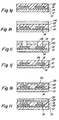
- Figs. 1a - 1n are diagrammatic side cross-sectional views of what is called here a "reverse neo process”.
- Fig. 1a begins with the preparation of aluminum shim stock 10. In the illustrated embodiment of aluminum shim stock is approximate 30 mills in thickness.
- a polyimide layer 12 is then disposed on aluminum layer 10. The polyimide layer is cured.
- a field metal layer 14 is applied on top of cured polyimide layer 12. Photoresist 16 is then disposed on metal layer 14 as shown in the side diagrammatic view of Fig. 1d and lithographically patterned according to conventional techniques.
- Gold or other conductive metal 18 is then disposed into openings and 20 defined in photoresist layers 16 as shown in Fig. 1e .
- the photoresist layer is then removed and field metal 14 etched leaving the structure depicted in Fig. 1f in which gold pads 18 are supported on field metal 14 on top of a polyimide coated aluminum shim 10.
- a polyimide layer 22 is then disposed on gold pads 18 of Fig. 1f .
- a photoresist layer 24 is then disposed upon polyimide layer 22 as depicted in Fig. 1h .
- Photo resist layer 25 is imaged and developed along with polyimide layer 20 to thereby define openings 26 through polyimide layer 24 and photoresist layer 22 to expose a selected portion of gold pad 18 as shown Fig. 1i .
- photoresist layer 24 is removed and polyimide layer 22 is cured leaving the structure shown in Fig. 1j in which openings 26 remain defined above gold pads 18.
- a field in the layer metal 26 is then disposed on polyimide layer 22 into openings 26 which have been previously defined above gold pads 18 to create a field metal layer 28 in which pockets or wells 30 are defined.
- a photoresist layer 32 is then disposed on top of field layer 28 as shown in Fig. 1l .
- Photoresist layer 32 is imaged and developed to define openings 34 into which a gold layer 36 is electroplated as shown in Fig. 1m .
- Photoresist layer 32 is then stripped away and field layer 28 is etched to leave the resulting structure as shown in Fig. 1n in which there are gold contact pads 36 positioned on top polyimide layer 22, which gold contact pads 36 in turn are connected to gold pads18 which are lying there below.
- Figs. 1a - 1n depict the process by which a metallization layer is constructed. If additional metallization layers are desired, the steps of Figs. 1g - 1n can be repeated as many times as necessary to created additional stacked layers of interconnects. In practice 3 or 4 layers are usually the most number ever needed.
- Figs. 2a - 2c represent the solder bumping of the die.
- a die 40 is obtained from a semiconductor wafer. It is to be understood the die 40 has been previously processed and may have any type of device or semiconductor devices already defined within it.
- Fig. 2b a plurality of metallic bumps are then applied in a predefined pattern on upper surface 44 of die 40 to provide contact to connection points on die 40.
- the solder layers 46 are then disposed on each of bumps 42 to result in the structure shown in Fig. 2c .
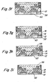
- Fig. 3a illustrates the flip chip bonding steps of the invention.
- the intermediate structure as shown in the completed step in Fig. 1n , is combined with the intermediate structure shown in the completed step of Fig. 2c .
- the structure of Fig.1n is for the purposes of Fig. 3a denoted collectively by reference numeral 48.
- the completed structure Fig. 2c is shown in Fig. 3a collectively denoted by the reference numeral 50.
- Die structure 50 is thus flipped and placed on top of interconnect structure 48 as depicted in Fig. 3a .
- the solder bumps 46 had been devised so they are aligned with gold contact pads 36.
- the flip structures are then bonded together to make secure mechanical and electrical connection at their points of contact.
- Fig. 3b The open space 52 between die structure 50 and interconnect structure 48 shown in Fig. 3a is filled with an insulating material 54 such as an epoxy under fill. Thereafter the entire bonded and completed structure as shown in Fig. 3b is potted with conventional potting material to form a monolithic passivated package as shown in Fig. 3c .
- Potted die structure 50 is thinned by grinding or other means to the desired final thickness forming a thin semiconductor wafer 56 as shown in Fig. 3d .
- Active semiconductor devices remain unaffected in the nonthinned or remaining portion of wafer 56.
- Aluminum layer 10, which has served the purpose of a structural substrate during the construction steps is then released by conventional means in step 3e and removed leaving polyimide layer 12 as the lowermost layer of the device as depicted in Fig. 3e .
- a masking layer 58 of photoresist is then disposed on polyimide layer 12 as shown in Fig. 3f and is photolithographically imaged to define openings 60 which will serve to provide the structure for the test pads 14, 18.
- the exposed polyimide layer 12 in openings 60 is then etched away to expose field layer metal 14 of gold pads 18.
- Etched mask 58 is then removed as shown in Fig. 3h . This then allows the semiconductor devices in thinned wafer 56 to be accessed and tested through test pads 14, 18 through openings 62 in polyimide layer 12.
- Fig. 4a is a diagrammatic side cross-sectional view of a further embodiment of the reverse neo process for high-volume fabrication.
- a first set of wafers generally to know by reference numeral 70, is processed along with a second wafer 72.
- An interconnect layer 74 such as described in connection Figs. 1a-1n is prepared and prepackaged chip devices 76 are then flip bonded to interconnect layer 74.
- the first wafer 70 includes a flash and SRAM memory chip and the second wafer includes an ASIC chip. It is of course to be understood that any number and kind of the packaged integrated circuit chips may be employed.
- the epoxies are cured, the devices underfilled and the transfer devices are molded to form the electronics packaged using potting 78 in the manner as described above.
- Fig. 4b the two wafers of Fig. 4a are combined. Any carriers which may be present on either wafer is released from the wafer substrate and the two wafers are attached or epoxied together as shown in Fig. 4b .
- wafers 70 and 72 which now form a collective package or stack that is denoted by reference normal 80, are cut or sawn into strips.
- metallizations within interconnect layers 74 are then connected together in a conventional manner through metallizations 82 defined on side surface 84 of stack 80.
- Numerous patents of the assignee of the present invention describe side connection technologies for vertical stacks of prepackaged devices.
- the upper surface of wafer 70 as shown in Fig. 4d of stack 80 is then thinned by grinding or other equivalent means.
- the lower portion of stack 80, wafer 72, is then solder bumped as shown in Fig. 4e , thereby providing a plurality of solder bumps 84 available for subsequent electrical connection.
- the strip of stacked wafers are then singulated or sawed into individual stacks 80 and are made available for subsequent processing or immediate installation.
- a packaged chip made according to the invention enjoys several advantages.
- the fabrication of the interconnect assembly 48 of Fig. 1n is isolated and independent of the fabrication of the chip assembly 50 of Fig. 2c so that chip assembly 50 are not subjected to the higher processing temperatures used in fabricating interconnect assembly 48. This is important, for example, where chip assembly 50 is a superconducting chip and is made of materials which cannot withstand conventional manufacturing temperatures.
- interconnect assembly 48 of Fig. 1n any failures or loss of yields in making the interconnect assembly 48 of Fig. 1n are not imposed on yields of the more expensive chip assembly 50.
- interconnect assembly 48 is fully tested and passed before bonding to chip assembly 50 in Fig. 3a , thereby increasing overall yields of the process.
- the process lends itself to a fabrication technology in which a larger number of dies at higher densities can be simultaneously processed than was possible with the prior neo-wafer processes.
- the methodology of the invention lends itself to an increase in the number of metallization layers within interconnect assembly 48 that can be realized as compared to the prior neo-wafer processes.
Landscapes
- Wire Bonding (AREA)
- Testing Or Measuring Of Semiconductors Or The Like (AREA)
- Production Of Multi-Layered Print Wiring Board (AREA)
- Tests Of Electronic Circuits (AREA)
- Credit Cards Or The Like (AREA)
Claims (14)
- Ein Verfahren zum Bereitstellen eines vorgeformten Integrierter-Schaltkreis-Chips (40) zum Verkapseln in einem elektronischen Gehäuse, die folgenden Schritte aufweisend:Bilden einer Zusammenschalt-Anordnung (48) getrennt von dem vorgeformten Integrierter-Schaltkreis-Chip (40),Bilden einer Mehrzahl von leitfähigen Höckern (42), die mit den Anschlüssen des vorgeformten Integrierter-Schaltkreis-Chips (40) verbunden sind,Bonden der Zusammenschalt-Anordnung (48) an den vorgeformten Integrierter-Schaltkreis-Chip (40),Passivieren der gebondeten Zusammenschalt-Anordnung (48) und des vorgeformten Integrierter-Schaltkreis-Chips (40) zu einer integralen Struktur, undVerdünnen des vorgeformten Integrierter-Schaltkreis-Chips (40) zum Bereitstellen des elektronischen Gehäuses,wobei das Verfahren ferner eine Mehrzahl von Zusammenschalt-Anordnungen (48) und vorgeformten Integrierter-Schaltkreis-Chips (40) aufweist, wobei die Mehrzahl von Zusammenschalt-Anordnungen (48) und vorgeformten Integrierter-Schaltkreis-Chips (40) zum Bilden einer jeweiligen Mehrzahl von elektronischen Gehäusen zusammengebondet wird, und ferner den Schritt des Testens der Zusammenschalt-Anordnung (48) und des Bondens einer getesteten Zusammenschalt-Anordnung (48) während des Schrittes des Bondens der Zusammenschalt-Anordnung (48) an den vorbereiteten Integrierter-Schaltkreis-Chip (40) nur dann, wenn die Zusammensahalt-Anordnung (48) als gut getestet wird, aufweist.
- Das Verfahren gemäß Anspruch 1, wobei der Schritt des Bildens der Zusammenschalt-Anordnung (48) das Bilden der Zusammenschalt-Anordnung auf einem lösbaren Substrat (10) aufweist.
- Das Verfahren gemäß Anspruch 1, wobei der Schritt des Bildens der Zusammenschalt-Anordnung (48) das Bilden von mindestens einem Testpad (14, 18) in einer Verbindungsschicht aufweist, wobei das mindestens eine Testpad (14, 18) an entgegengesetzten Seiten des mindestens einen Testpads zugänglich ist und elektrisch verbunden werden kann.
- Das Verfahren gemäß Anspruch 3, wobei der Schritt des Bildens mindestens eines Testpads (14, 18) ein Testpad bildet, das Gold auf einem leitfähigen Feldmetall aufweist.
- Das Verfahren gemäß Anspruch 3, wobei der Schritt des Bildens der Zusammenschalt-Anordnung (48) das Bilden mindestens eines Testpads (14, 18) in einer Mehrzahl von gestapelten Verbindungsschichten aufweist, wobei jedes von dem mindestens einen Testpad (14, 18) in jeder Verbindungsschicht an entgegengesetzten Seiten des mindestens einen Testpads zugänglich ist und elektrisch verbunden werden kann.
- Das Verfahren gemäß Anspruch 5, wobei der Schritt des Bildens von mindestens einem Testpad (14, 18) in der Mehrzahl von gestapelten Verbindungsschichten mindestens ein Testpad in jeder Schicht bildet, das Gold auf einem leitfähigen Feldmetall aufweist.
- Das Verfahren gemäß Anspruch 1, wobei der Schritt des Bildens der Mehrzahl von leitfähigen Höckern (42), die mit den Anschlüssen des Integrierter-Schaltkreis-Chips (40) verbunden sind, einen Metall-Höcker (42) bildet, der eine Verbindung mit einem Anschluss auf dem Integrierter-Schaltkreis-Chip (40) und einer Lötschicht (46) herstellt, die auf dem Metallhöcker (42) angeordnet ist.
- Das Verfahren gemäß Anspruch 7, wobei der Schritt des Bildens der Zusammenschalt-Anordnung (48) das Bilden mindestens eines Testpads (14, 18) in einer Verbindungsschicht aufweist, wobei das mindestens eine Testpad (14, 18) an entgegengesetzten Seiten des Testpads zugänglich ist und elektrisch verbunden werden kann, und wobei der Schritt des Bondens der Zusammenschalt-Anordnung (48) an den vorgeformten Integrierter-Schaltkreis-Chip (40) die Lötschicht (46) an eine Seite des Testpads (14, 18) flip-bondet.
- Das Verfahren gemäß Anspruch 1, wobei der Schritt des Passivierens der gebondeten Zusammenschalt-Anordnung (48) und des vorgeformten Integrierter-Schaltkreis-Chips (40) zu der integralen Struktur zum Bereitstellen des elektronischen Gehäuses das Unterfüllen des vorbereiteten Integrierter-Schaltkreis-Chips (40) mit einem Isolationsmaterial (54) aufweist, zum Entfernen aller Lücken zwischen dem vorgeformten Integrierter-Schaltkreis-Chip (40) und der Zusammenschalt-Anordnung (48).
- Das Verfahren gemäß Anspruch 1, wobei der Schritt des Passivierens der gebondeten Zusammenschalt-Anordnung (48) und des vorgeformten Integrierter-Schaltkreis-Chips (40) zu der integralen Struktur zum Bereitstellen des elektronischen Gehäuses das Vergießen der Zusammenschalt-Anordnung (48) und des vorbereiteten Integrierter-Schaltkreis-Chips (40) in ein integrales Gehäuse aufweist.
- Das Verfahren gemäß Anspruch 9, wobei der Schritt des Passivierens der gebondeten Zusammenschalt-Anordnung (48) und des vorgeformten Integrierter-Schaltkreis-Chips (40) zu der integralen Struktur zum Bereitstellen des elektronischen Gehäuses das Vergießen der Zusammenschalt-Anordnung (48) und des vorgeformten Integrierter-Schaltkreis-Chips (40) in ein integrales Gehäuse aufweist.
- Das Verfahren gemäß Anspruch 10, ferner aufweisend einen Schritt des Zugreifens auf den vorgeformten Integrierter-Schaltkreis-Chip (40) durch elektrische Verbindung mit mindestens einem Testpad (14, 18) durch eine Oberfläche davon entgegengesetzt zu der Fläche des mindestens einen Testpads (14, 18), das einen Anschluss des vorgeformten Integrierter-Schaltkreis-Chips (40) kontaktiert, zum Testen des vorgeformten Integrierter-Schaltkreis-Chips (40).
- Das Verfahren gemäß Anspruch 10, ferner eine Mehrzahl einer Zusammenschalt-Anordnung (48) und vorgeformten Integrierter-Schaltkreis-Chips (40) aufweisend, wobei die Mehrzahl der Zusammenschalt-Anordnungen (48) und vorgeformten Integrierter-Schaltkreis-Chips (40) zum Bilden einer jeweiligen Mehrzahl von elektronischen Gehäusen zusammengebondet sind, und ferner den Schritt des Lösens der Mehrzahl von elektronischen Gehäusen voneinander aufweisend.
- Das Verfahren gemäß Anspruch 1, wobei der Schritt des Bildens der Mehrzahl von Zusammenschalt-Anordnungen (48) das gleichzeitige Bilden der Zusammenschalt-Anordnungen in einem Wafer aufweist, und wobei die Mehrzahl von vorgeformten Integrierter-Schaltkreis-Chips (40) einzeln an erfolgreich getestete der Zusammenschalt-Anordnungen (48) höcker-gebondet sind.
Priority Applications (2)
| Application Number | Priority Date | Filing Date | Title |
|---|---|---|---|
| EP09164532A EP2101349A3 (de) | 2001-10-30 | 2002-10-25 | Stapelbare Schichten, die eingekapselte integrierte Schaltungschips mit einer oder mehreren darüberliegenden Verbindungsschichten beinhalten und Verfahren zu deren Herstellung |
| EP13199181.2A EP2711976A2 (de) | 2001-10-30 | 2002-10-25 | Stapelbare Schichten, die eingekapselte integrierte Schaltungschips mit einer oder mehreren darüberliegenden Verbindungsschichten beinhalten und Verfahren zu deren Herstellung |
Applications Claiming Priority (3)
| Application Number | Priority Date | Filing Date | Title |
|---|---|---|---|
| US938686 | 1997-09-26 | ||
| US09/938,686 US6797537B2 (en) | 2001-10-30 | 2001-10-30 | Method of making stackable layers containing encapsulated integrated circuit chips with one or more overlaying interconnect layers |
| PCT/US2002/034339 WO2003038861A2 (en) | 2001-10-30 | 2002-10-25 | A method of stacking layers containing encapsulated integrated circuit chips with one or more overlying interconnect layers |
Related Child Applications (2)
| Application Number | Title | Priority Date | Filing Date |
|---|---|---|---|
| EP09164532A Division EP2101349A3 (de) | 2001-10-30 | 2002-10-25 | Stapelbare Schichten, die eingekapselte integrierte Schaltungschips mit einer oder mehreren darüberliegenden Verbindungsschichten beinhalten und Verfahren zu deren Herstellung |
| EP13199181.2A Division EP2711976A2 (de) | 2001-10-30 | 2002-10-25 | Stapelbare Schichten, die eingekapselte integrierte Schaltungschips mit einer oder mehreren darüberliegenden Verbindungsschichten beinhalten und Verfahren zu deren Herstellung |
Publications (3)
| Publication Number | Publication Date |
|---|---|
| EP1576649A2 EP1576649A2 (de) | 2005-09-21 |
| EP1576649A4 EP1576649A4 (de) | 2006-11-15 |
| EP1576649B1 true EP1576649B1 (de) | 2009-09-30 |
Family
ID=25471798
Family Applications (3)
| Application Number | Title | Priority Date | Filing Date |
|---|---|---|---|
| EP13199181.2A Withdrawn EP2711976A2 (de) | 2001-10-30 | 2002-10-25 | Stapelbare Schichten, die eingekapselte integrierte Schaltungschips mit einer oder mehreren darüberliegenden Verbindungsschichten beinhalten und Verfahren zu deren Herstellung |
| EP02789292A Expired - Lifetime EP1576649B1 (de) | 2001-10-30 | 2002-10-25 | Stapelbare schichten die eingekapselte integrierte schaltungschips mit einer oder mehreren darüberliegenden verbindungsschichten beinhalten und verfahren zu deren herstellung |
| EP09164532A Withdrawn EP2101349A3 (de) | 2001-10-30 | 2002-10-25 | Stapelbare Schichten, die eingekapselte integrierte Schaltungschips mit einer oder mehreren darüberliegenden Verbindungsschichten beinhalten und Verfahren zu deren Herstellung |
Family Applications Before (1)
| Application Number | Title | Priority Date | Filing Date |
|---|---|---|---|
| EP13199181.2A Withdrawn EP2711976A2 (de) | 2001-10-30 | 2002-10-25 | Stapelbare Schichten, die eingekapselte integrierte Schaltungschips mit einer oder mehreren darüberliegenden Verbindungsschichten beinhalten und Verfahren zu deren Herstellung |
Family Applications After (1)
| Application Number | Title | Priority Date | Filing Date |
|---|---|---|---|
| EP09164532A Withdrawn EP2101349A3 (de) | 2001-10-30 | 2002-10-25 | Stapelbare Schichten, die eingekapselte integrierte Schaltungschips mit einer oder mehreren darüberliegenden Verbindungsschichten beinhalten und Verfahren zu deren Herstellung |
Country Status (6)
| Country | Link |
|---|---|
| US (3) | US6797537B2 (de) |
| EP (3) | EP2711976A2 (de) |
| AT (1) | ATE444564T1 (de) |
| AU (1) | AU2002353894A1 (de) |
| DE (1) | DE60233902D1 (de) |
| WO (1) | WO2003038861A2 (de) |
Families Citing this family (35)
| Publication number | Priority date | Publication date | Assignee | Title |
|---|---|---|---|---|
| US7440449B2 (en) * | 2000-10-06 | 2008-10-21 | Irvine Sensors Corp. | High speed switching module comprised of stacked layers incorporating t-connect structures |
| US7242082B2 (en) | 2002-02-07 | 2007-07-10 | Irvine Sensors Corp. | Stackable layer containing ball grid array package |
| SG115459A1 (en) * | 2002-03-04 | 2005-10-28 | Micron Technology Inc | Flip chip packaging using recessed interposer terminals |
| US6806559B2 (en) * | 2002-04-22 | 2004-10-19 | Irvine Sensors Corporation | Method and apparatus for connecting vertically stacked integrated circuit chips |
| US7777321B2 (en) * | 2002-04-22 | 2010-08-17 | Gann Keith D | Stacked microelectronic layer and module with three-axis channel T-connects |
| US6998328B2 (en) * | 2002-11-06 | 2006-02-14 | Irvine Sensors Corp. | Method for creating neo-wafers from singulated integrated circuit die and a device made according to the method |
| US7198965B2 (en) * | 2002-11-06 | 2007-04-03 | Irvine Sensors Corp. | Method for making a neo-layer comprising embedded discrete components |
| US20050184368A1 (en) * | 2003-01-21 | 2005-08-25 | Huang Chien P. | Semiconductor package free of substrate and fabrication method thereof |
| JP2007521631A (ja) * | 2003-08-08 | 2007-08-02 | アービン センサーズ コーポレーション | 積層可能な層及びその製造方法 |
| WO2006018787A2 (en) * | 2004-08-20 | 2006-02-23 | Philips Intellectual Property & Standards Gmbh | Method of detaching a thin semiconductor circuit from its base |
| US7268012B2 (en) * | 2004-08-31 | 2007-09-11 | Micron Technology, Inc. | Methods for fabrication of thin semiconductor assemblies including redistribution layers and packages and assemblies formed thereby |
| EP1724835A1 (de) | 2005-05-17 | 2006-11-22 | Irvine Sensors Corporation | Elektronischer Baustein mit einer Lage, die eine integrierte Schaltung enthält und dessen Herstellung |
| US7768113B2 (en) * | 2005-05-26 | 2010-08-03 | Volkan Ozguz | Stackable tier structure comprising prefabricated high density feedthrough |
| US7919844B2 (en) * | 2005-05-26 | 2011-04-05 | Aprolase Development Co., Llc | Tier structure with tier frame having a feedthrough structure |
| JP5065586B2 (ja) * | 2005-10-18 | 2012-11-07 | ルネサスエレクトロニクス株式会社 | 半導体装置の製造方法 |
| JP2007115958A (ja) * | 2005-10-21 | 2007-05-10 | Seiko Epson Corp | 半導体装置 |
| US7645638B2 (en) * | 2006-08-04 | 2010-01-12 | Stats Chippac Ltd. | Stackable multi-chip package system with support structure |
| US8432026B2 (en) * | 2006-08-04 | 2013-04-30 | Stats Chippac Ltd. | Stackable multi-chip package system |
| US7622333B2 (en) * | 2006-08-04 | 2009-11-24 | Stats Chippac Ltd. | Integrated circuit package system for package stacking and manufacturing method thereof |
| US8110899B2 (en) * | 2006-12-20 | 2012-02-07 | Intel Corporation | Method for incorporating existing silicon die into 3D integrated stack |
| KR100843718B1 (ko) | 2007-01-25 | 2008-07-04 | 삼성전자주식회사 | 접착 물질에 기인된 보이드에 면역력을 가지는 반도체패키지들 및 그 형성방법들 |
| KR100887475B1 (ko) * | 2007-02-26 | 2009-03-10 | 주식회사 네패스 | 반도체 패키지 및 그 제조방법 |
| US7714426B1 (en) | 2007-07-07 | 2010-05-11 | Keith Gann | Ball grid array package format layers and structure |
| US7863918B2 (en) | 2007-11-13 | 2011-01-04 | International Business Machines Corporation | Disposable built-in self-test devices, systems and methods for testing three dimensional integrated circuits |
| TWI455263B (zh) * | 2009-02-16 | 2014-10-01 | 財團法人工業技術研究院 | 晶片封裝結構及晶片封裝方法 |
| US9431275B2 (en) | 2010-09-17 | 2016-08-30 | Pfg Ip Llc | Wire bond through-via structure and method |
| US8609473B2 (en) | 2010-09-17 | 2013-12-17 | ISC8 Inc. | Method for fabricating a neo-layer using stud bumped bare die |
| US8649820B2 (en) | 2011-11-07 | 2014-02-11 | Blackberry Limited | Universal integrated circuit card apparatus and related methods |
| US8936199B2 (en) | 2012-04-13 | 2015-01-20 | Blackberry Limited | UICC apparatus and related methods |
| USD703208S1 (en) | 2012-04-13 | 2014-04-22 | Blackberry Limited | UICC apparatus |
| USD701864S1 (en) * | 2012-04-23 | 2014-04-01 | Blackberry Limited | UICC apparatus |
| US9196504B2 (en) | 2012-07-03 | 2015-11-24 | Utac Dongguan Ltd. | Thermal leadless array package with die attach pad locking feature |
| US9023690B2 (en) * | 2012-11-19 | 2015-05-05 | United Test And Assembly Center | Leadframe area array packaging technology |
| US9564387B2 (en) | 2014-08-28 | 2017-02-07 | UTAC Headquarters Pte. Ltd. | Semiconductor package having routing traces therein |
| US11670614B2 (en) * | 2020-10-02 | 2023-06-06 | Qualcomm Incorporated | Integrated circuit assembly with hybrid bonding |
Family Cites Families (7)
| Publication number | Priority date | Publication date | Assignee | Title |
|---|---|---|---|---|
| HUT73312A (en) * | 1992-09-14 | 1996-07-29 | Badehi | Method and apparatus for producing integrated circuit devices, and integrated circuit device |
| JP3537447B2 (ja) * | 1996-10-29 | 2004-06-14 | トル‐シ・テクノロジーズ・インコーポレイテッド | 集積回路及びその製造方法 |
| US5953588A (en) * | 1996-12-21 | 1999-09-14 | Irvine Sensors Corporation | Stackable layers containing encapsulated IC chips |
| US6329832B1 (en) * | 1998-10-05 | 2001-12-11 | Micron Technology, Inc. | Method for in-line testing of flip-chip semiconductor assemblies |
| US6117704A (en) * | 1999-03-31 | 2000-09-12 | Irvine Sensors Corporation | Stackable layers containing encapsulated chips |
| KR100298827B1 (ko) * | 1999-07-09 | 2001-11-01 | 윤종용 | 재배선 기판을 사용한 웨이퍼 레벨 칩 스케일 패키지 제조방법 |
| JP2001144218A (ja) * | 1999-11-17 | 2001-05-25 | Sony Corp | 半導体装置及び半導体装置の製造方法 |
-
2001
- 2001-10-30 US US09/938,686 patent/US6797537B2/en not_active Expired - Lifetime
-
2002
- 2002-10-25 EP EP13199181.2A patent/EP2711976A2/de not_active Withdrawn
- 2002-10-25 EP EP02789292A patent/EP1576649B1/de not_active Expired - Lifetime
- 2002-10-25 WO PCT/US2002/034339 patent/WO2003038861A2/en not_active Ceased
- 2002-10-25 AT AT02789292T patent/ATE444564T1/de not_active IP Right Cessation
- 2002-10-25 DE DE60233902T patent/DE60233902D1/de not_active Expired - Lifetime
- 2002-10-25 EP EP09164532A patent/EP2101349A3/de not_active Withdrawn
- 2002-10-25 AU AU2002353894A patent/AU2002353894A1/en not_active Abandoned
- 2002-11-21 US US10/302,680 patent/US6784547B2/en not_active Expired - Lifetime
-
2004
- 2004-09-28 US US10/951,990 patent/US7239012B2/en not_active Expired - Lifetime
Also Published As
| Publication number | Publication date |
|---|---|
| US6784547B2 (en) | 2004-08-31 |
| US6797537B2 (en) | 2004-09-28 |
| EP1576649A2 (de) | 2005-09-21 |
| WO2003038861A3 (en) | 2005-12-29 |
| AU2002353894A1 (en) | 2003-05-12 |
| ATE444564T1 (de) | 2009-10-15 |
| US7239012B2 (en) | 2007-07-03 |
| EP2101349A2 (de) | 2009-09-16 |
| US20030127735A1 (en) | 2003-07-10 |
| WO2003038861A2 (en) | 2003-05-08 |
| EP2101349A3 (de) | 2011-08-17 |
| US20030080419A1 (en) | 2003-05-01 |
| EP1576649A4 (de) | 2006-11-15 |
| US20050037540A1 (en) | 2005-02-17 |
| EP2711976A2 (de) | 2014-03-26 |
| DE60233902D1 (de) | 2009-11-12 |
Similar Documents
| Publication | Publication Date | Title |
|---|---|---|
| EP1576649B1 (de) | Stapelbare schichten die eingekapselte integrierte schaltungschips mit einer oder mehreren darüberliegenden verbindungsschichten beinhalten und verfahren zu deren herstellung | |
| US12564109B2 (en) | Package component, electronic device and manufacturing method thereof | |
| US7198980B2 (en) | Methods for assembling multiple semiconductor devices | |
| US12074131B2 (en) | Package structure and manufacturing method thereof | |
| US6117704A (en) | Stackable layers containing encapsulated chips | |
| US7573136B2 (en) | Semiconductor device assemblies and packages including multiple semiconductor device components | |
| CN103718289B (zh) | 半导体裸片组合件、包含所述半导体裸片组合件的半导体装置及制造方法 | |
| US7919844B2 (en) | Tier structure with tier frame having a feedthrough structure | |
| US20180374797A1 (en) | Integrated fan-out package and method of fabricating the same | |
| US20170229426A1 (en) | Fan-out back-to-back chip stacked packages and the method for manufacturing the same | |
| US20080136004A1 (en) | Multi-chip package structure and method of forming the same | |
| US20220165675A1 (en) | Semiconductor structure and method of fabricating the same | |
| US20240379491A1 (en) | Method of manufacturing semiconductor package | |
| US20250357353A1 (en) | Semiconductor package and manufacturing method thereof | |
| US7768113B2 (en) | Stackable tier structure comprising prefabricated high density feedthrough | |
| EP1596433B1 (de) | Verfahren zur Erstellung einer Halbleiterscheibe aus integrierten Schaltungschips sowie nach diesem Verfahren hergestellte Vorrichtung | |
| US20120326300A1 (en) | Low profile package and method | |
| CN113838840B (zh) | 半导体封装及制造半导体封装的方法 | |
| CN114883196A (zh) | 半导体器件及其制造方法 | |
| US7417323B2 (en) | Neo-wafer device and method | |
| CN114695324A (zh) | 半导体封装结构及其制造方法 |
Legal Events
| Date | Code | Title | Description |
|---|---|---|---|
| PUAI | Public reference made under article 153(3) epc to a published international application that has entered the european phase |
Free format text: ORIGINAL CODE: 0009012 |
|
| 17P | Request for examination filed |
Effective date: 20040920 |
|
| AK | Designated contracting states |
Kind code of ref document: A2 Designated state(s): AT BE BG CH CY CZ DE DK EE ES FI FR GB GR IE IT LI LU MC NL PT SE SK TR |
|
| PUAK | Availability of information related to the publication of the international search report |
Free format text: ORIGINAL CODE: 0009015 |
|
| RIC1 | Information provided on ipc code assigned before grant |
Ipc: H01L 21/44 20060101AFI20060105BHEP Ipc: H01L 23/48 20060101ALI20060105BHEP |
|
| A4 | Supplementary search report drawn up and despatched |
Effective date: 20061016 |
|
| 17Q | First examination report despatched |
Effective date: 20070726 |
|
| RIC1 | Information provided on ipc code assigned before grant |
Ipc: H01L 21/44 20060101AFI20090217BHEP Ipc: H01L 23/48 20060101ALI20090217BHEP Ipc: H01L 21/68 20060101ALI20090217BHEP Ipc: H01L 23/31 20060101ALI20090217BHEP Ipc: H01L 23/58 20060101ALI20090217BHEP Ipc: H01L 23/538 20060101ALI20090217BHEP |
|
| GRAP | Despatch of communication of intention to grant a patent |
Free format text: ORIGINAL CODE: EPIDOSNIGR1 |
|
| RAP1 | Party data changed (applicant data changed or rights of an application transferred) |
Owner name: APROLASE DEVELOPMENT CO., LLC |
|
| GRAS | Grant fee paid |
Free format text: ORIGINAL CODE: EPIDOSNIGR3 |
|
| GRAA | (expected) grant |
Free format text: ORIGINAL CODE: 0009210 |
|
| AK | Designated contracting states |
Kind code of ref document: B1 Designated state(s): AT BE BG CH CY CZ DE DK EE ES FI FR GB GR IE IT LI LU MC NL PT SE SK TR |
|
| REG | Reference to a national code |
Ref country code: GB Ref legal event code: FG4D Ref country code: CH Ref legal event code: EP |
|
| REG | Reference to a national code |
Ref country code: IE Ref legal event code: FG4D |
|
| REF | Corresponds to: |
Ref document number: 60233902 Country of ref document: DE Date of ref document: 20091112 Kind code of ref document: P |
|
| PG25 | Lapsed in a contracting state [announced via postgrant information from national office to epo] |
Ref country code: SE Free format text: LAPSE BECAUSE OF FAILURE TO SUBMIT A TRANSLATION OF THE DESCRIPTION OR TO PAY THE FEE WITHIN THE PRESCRIBED TIME-LIMIT Effective date: 20090930 Ref country code: FI Free format text: LAPSE BECAUSE OF FAILURE TO SUBMIT A TRANSLATION OF THE DESCRIPTION OR TO PAY THE FEE WITHIN THE PRESCRIBED TIME-LIMIT Effective date: 20090930 |
|
| NLV1 | Nl: lapsed or annulled due to failure to fulfill the requirements of art. 29p and 29m of the patents act | ||
| PG25 | Lapsed in a contracting state [announced via postgrant information from national office to epo] |
Ref country code: PT Free format text: LAPSE BECAUSE OF FAILURE TO SUBMIT A TRANSLATION OF THE DESCRIPTION OR TO PAY THE FEE WITHIN THE PRESCRIBED TIME-LIMIT Effective date: 20100201 Ref country code: EE Free format text: LAPSE BECAUSE OF FAILURE TO SUBMIT A TRANSLATION OF THE DESCRIPTION OR TO PAY THE FEE WITHIN THE PRESCRIBED TIME-LIMIT Effective date: 20090930 Ref country code: CZ Free format text: LAPSE BECAUSE OF FAILURE TO SUBMIT A TRANSLATION OF THE DESCRIPTION OR TO PAY THE FEE WITHIN THE PRESCRIBED TIME-LIMIT Effective date: 20090930 Ref country code: ES Free format text: LAPSE BECAUSE OF FAILURE TO SUBMIT A TRANSLATION OF THE DESCRIPTION OR TO PAY THE FEE WITHIN THE PRESCRIBED TIME-LIMIT Effective date: 20100110 |
|
| PG25 | Lapsed in a contracting state [announced via postgrant information from national office to epo] |
Ref country code: CY Free format text: LAPSE BECAUSE OF FAILURE TO SUBMIT A TRANSLATION OF THE DESCRIPTION OR TO PAY THE FEE WITHIN THE PRESCRIBED TIME-LIMIT Effective date: 20090930 Ref country code: SK Free format text: LAPSE BECAUSE OF FAILURE TO SUBMIT A TRANSLATION OF THE DESCRIPTION OR TO PAY THE FEE WITHIN THE PRESCRIBED TIME-LIMIT Effective date: 20090930 Ref country code: MC Free format text: LAPSE BECAUSE OF NON-PAYMENT OF DUE FEES Effective date: 20091031 |
|
| REG | Reference to a national code |
Ref country code: CH Ref legal event code: PL |
|
| PG25 | Lapsed in a contracting state [announced via postgrant information from national office to epo] |
Ref country code: BE Free format text: LAPSE BECAUSE OF FAILURE TO SUBMIT A TRANSLATION OF THE DESCRIPTION OR TO PAY THE FEE WITHIN THE PRESCRIBED TIME-LIMIT Effective date: 20090930 Ref country code: AT Free format text: LAPSE BECAUSE OF FAILURE TO SUBMIT A TRANSLATION OF THE DESCRIPTION OR TO PAY THE FEE WITHIN THE PRESCRIBED TIME-LIMIT Effective date: 20090930 |
|
| PG25 | Lapsed in a contracting state [announced via postgrant information from national office to epo] |
Ref country code: DK Free format text: LAPSE BECAUSE OF FAILURE TO SUBMIT A TRANSLATION OF THE DESCRIPTION OR TO PAY THE FEE WITHIN THE PRESCRIBED TIME-LIMIT Effective date: 20090930 Ref country code: NL Free format text: LAPSE BECAUSE OF FAILURE TO SUBMIT A TRANSLATION OF THE DESCRIPTION OR TO PAY THE FEE WITHIN THE PRESCRIBED TIME-LIMIT Effective date: 20090930 |
|
| PLBE | No opposition filed within time limit |
Free format text: ORIGINAL CODE: 0009261 |
|
| STAA | Information on the status of an ep patent application or granted ep patent |
Free format text: STATUS: NO OPPOSITION FILED WITHIN TIME LIMIT |
|
| 26N | No opposition filed |
Effective date: 20100701 |
|
| PG25 | Lapsed in a contracting state [announced via postgrant information from national office to epo] |
Ref country code: LI Free format text: LAPSE BECAUSE OF NON-PAYMENT OF DUE FEES Effective date: 20091031 Ref country code: IE Free format text: LAPSE BECAUSE OF NON-PAYMENT OF DUE FEES Effective date: 20091025 Ref country code: GR Free format text: LAPSE BECAUSE OF FAILURE TO SUBMIT A TRANSLATION OF THE DESCRIPTION OR TO PAY THE FEE WITHIN THE PRESCRIBED TIME-LIMIT Effective date: 20091231 Ref country code: CH Free format text: LAPSE BECAUSE OF NON-PAYMENT OF DUE FEES Effective date: 20091031 |
|
| PG25 | Lapsed in a contracting state [announced via postgrant information from national office to epo] |
Ref country code: BG Free format text: LAPSE BECAUSE OF FAILURE TO SUBMIT A TRANSLATION OF THE DESCRIPTION OR TO PAY THE FEE WITHIN THE PRESCRIBED TIME-LIMIT Effective date: 20091031 Ref country code: IT Free format text: LAPSE BECAUSE OF FAILURE TO SUBMIT A TRANSLATION OF THE DESCRIPTION OR TO PAY THE FEE WITHIN THE PRESCRIBED TIME-LIMIT Effective date: 20090930 |
|
| PG25 | Lapsed in a contracting state [announced via postgrant information from national office to epo] |
Ref country code: LU Free format text: LAPSE BECAUSE OF NON-PAYMENT OF DUE FEES Effective date: 20091025 |
|
| PG25 | Lapsed in a contracting state [announced via postgrant information from national office to epo] |
Ref country code: TR Free format text: LAPSE BECAUSE OF FAILURE TO SUBMIT A TRANSLATION OF THE DESCRIPTION OR TO PAY THE FEE WITHIN THE PRESCRIBED TIME-LIMIT Effective date: 20090930 |
|
| REG | Reference to a national code |
Ref country code: FR Ref legal event code: PLFP Year of fee payment: 15 |
|
| REG | Reference to a national code |
Ref country code: FR Ref legal event code: PLFP Year of fee payment: 16 |
|
| REG | Reference to a national code |
Ref country code: FR Ref legal event code: PLFP Year of fee payment: 17 |
|
| PGFP | Annual fee paid to national office [announced via postgrant information from national office to epo] |
Ref country code: FR Payment date: 20210921 Year of fee payment: 20 |
|
| PGFP | Annual fee paid to national office [announced via postgrant information from national office to epo] |
Ref country code: GB Payment date: 20210929 Year of fee payment: 20 |
|
| PGFP | Annual fee paid to national office [announced via postgrant information from national office to epo] |
Ref country code: DE Payment date: 20210916 Year of fee payment: 20 |
|
| REG | Reference to a national code |
Ref country code: DE Ref legal event code: R071 Ref document number: 60233902 Country of ref document: DE |
|
| REG | Reference to a national code |
Ref country code: GB Ref legal event code: PE20 Expiry date: 20221024 |
|
| PG25 | Lapsed in a contracting state [announced via postgrant information from national office to epo] |
Ref country code: GB Free format text: LAPSE BECAUSE OF EXPIRATION OF PROTECTION Effective date: 20221024 |