EP1575143A2 - Spannungsausgleichsschaltung für Batteriezellen - Google Patents
Spannungsausgleichsschaltung für Batteriezellen Download PDFInfo
- Publication number
- EP1575143A2 EP1575143A2 EP04030303A EP04030303A EP1575143A2 EP 1575143 A2 EP1575143 A2 EP 1575143A2 EP 04030303 A EP04030303 A EP 04030303A EP 04030303 A EP04030303 A EP 04030303A EP 1575143 A2 EP1575143 A2 EP 1575143A2
- Authority
- EP
- European Patent Office
- Prior art keywords
- voltage
- battery
- elements
- windings
- minimum
- Prior art date
- Legal status (The legal status is an assumption and is not a legal conclusion. Google has not performed a legal analysis and makes no representation as to the accuracy of the status listed.)
- Withdrawn
Links
Images


Classifications
-
- H—ELECTRICITY
- H02—GENERATION; CONVERSION OR DISTRIBUTION OF ELECTRIC POWER
- H02J—ELECTRIC POWER NETWORKS; CIRCUIT ARRANGEMENTS OR SYSTEMS FOR SUPPLYING OR DISTRIBUTING ELECTRIC POWER; SYSTEMS FOR STORING ELECTRIC ENERGY
- H02J7/00—Circuit arrangements for charging or discharging batteries or for supplying loads from batteries
- H02J7/50—Circuit arrangements for charging or discharging batteries or for supplying loads from batteries acting upon multiple batteries simultaneously or sequentially
- H02J7/52—Circuit arrangements for charging or discharging batteries or for supplying loads from batteries acting upon multiple batteries simultaneously or sequentially for charge balancing, e.g. equalisation of charge between batteries
- H02J7/54—Passive balancing, e.g. using resistors or parallel MOSFETs
-
- B—PERFORMING OPERATIONS; TRANSPORTING
- B60—VEHICLES IN GENERAL
- B60L—PROPULSION OF ELECTRICALLY-PROPELLED VEHICLES; SUPPLYING ELECTRIC POWER FOR AUXILIARY EQUIPMENT OF ELECTRICALLY-PROPELLED VEHICLES; ELECTRODYNAMIC BRAKE SYSTEMS FOR VEHICLES IN GENERAL; MAGNETIC SUSPENSION OR LEVITATION FOR VEHICLES; MONITORING OPERATING VARIABLES OF ELECTRICALLY-PROPELLED VEHICLES; ELECTRIC SAFETY DEVICES FOR ELECTRICALLY-PROPELLED VEHICLES
- B60L50/00—Electric propulsion with power supplied within the vehicle
- B60L50/50—Electric propulsion with power supplied within the vehicle using propulsion power supplied by batteries or fuel cells
- B60L50/60—Electric propulsion with power supplied within the vehicle using propulsion power supplied by batteries or fuel cells using power supplied by batteries
-
- Y—GENERAL TAGGING OF NEW TECHNOLOGICAL DEVELOPMENTS; GENERAL TAGGING OF CROSS-SECTIONAL TECHNOLOGIES SPANNING OVER SEVERAL SECTIONS OF THE IPC; TECHNICAL SUBJECTS COVERED BY FORMER USPC CROSS-REFERENCE ART COLLECTIONS [XRACs] AND DIGESTS
- Y02—TECHNOLOGIES OR APPLICATIONS FOR MITIGATION OR ADAPTATION AGAINST CLIMATE CHANGE
- Y02T—CLIMATE CHANGE MITIGATION TECHNOLOGIES RELATED TO TRANSPORTATION
- Y02T10/00—Road transport of goods or passengers
- Y02T10/60—Other road transportation technologies with climate change mitigation effect
- Y02T10/70—Energy storage systems for electromobility, e.g. batteries
Definitions
- the present invention relates to a voltage equalizer for battery elements for equalizing terminal voltages of battery elements which constitute a battery or the like.
- a battery including a number of (for example, about one hundred) battery elements which are connected in series to each other is installed in an electric vehicle which is run by a motor or a hybrid vehicle which is run in combination of an engine and a motor. Then, a voltage equalizer is connected to the battery in consideration of securement of a charging capacity, extension of the life of each battery element and safety. Further, a voltage detector for detecting an abnormal terminal voltage of each battery element is also connected to the battery to eliminate a risk of the occurrence of a serious secondary failure which would be caused by heat and leakage of fluid which are caused in the event that there occurs a short circuit in one of the battery elements.
- a voltage equalizer for battery elements which was proposed by the applicant of the present invention and is disclosed in JP-A-2002-223528.
- a closed circuit is configured by battery elements of one of a plurality of groups of battery elements which are connected in series, each of a plurality of secondary windings which are magnetically connected to each other and each of one of pluralities of switching elements, and a closed circuit is configured by battery elements of the other group of battery elements, primary windings which are magnetically connected to the secondary windings in a common fashion and the other plurality of switching elements, whereby the output voltage of the one of a plurality of groups of battery elements which are connected in series is equalized by ON/OFF controlling the one of pluralities of switching elements and the other plurality of switching elements alternately.
- a voltage detection circuit for battery elements which has already been proposed by the applicant of the present invention and is disclosed in JP-2002-357625.
- This voltage detection circuit is a voltage detection circuit for battery elements for detecting a voltage between terminals of each of a plurality of battery elements which are connected in series to each other which has a voltage detection means connected between terminals of each of the plurality of battery elements and adapted to cause a detection current to flow from an output terminal when a predetermined voltage is reached and a single detection signal output means connected via a load resistance to a negative terminal of a battery element, which is positioned on a minimum potential side, of the plurality of battery elements which are connected in series to the output terminal of the voltage detecting means, whereby a sufficient current for the single detection signal output means to output a detection signal can securely be allowed to flow even in the event that any of the battery elements reaches a predetermined voltage which is set in advance.
- the invention was made in view of these situations, and an object thereof is to provide a voltage equalizer for battery elements which can solve the problems inherent in the background art.
- a voltage equalizer for battery elements for equalizing terminal voltages of a plurality of battery elements B... comprising an equalization processing circuit 6 having a transformer 2 having, in turn, basic windings 2o... made up of at least a plurality of primary windings 2a... which correspond, respectively, to the plurality of battery elements and one or two or more secondary windings 2b... , a plurality of switching elements 3... which correspond, respectively, to the battery elements B... , a plurality of primary diodes 5a... which correspond, respectively, to the battery elements B... , and one or two or more secondary diodes 5b... which correspond, respectively, to the secondary windings 2b...
- the basic windings 2o... may be made up of pluralities of primary windings 2a... and secondary windings 2b... which correspond, respectively, to the battery elements B... by separating the primary windings and the secondary windings with intermediate taps 2oc... .
- the basic windings 2o... may be made up of a single winding to be used both for the primary series circuits Ca... in the corresponding battery elements B... and the secondary series circuits Cb... in the other battery elements B...
- an auxiliary winding 2x may be provided in the transformer 2 for use as a secondary series circuit Cb in the battery elements B where the secondary series circuit is not configured depending upon the basic windings 2o.
- the basic windings 2o... may be made up of a plurality of primary windings 2a... which correspond, respectively, to the battery elements B... and one or two or more secondary windings 2b... which correspond, respectively, to groups G of one or two or more groups which results when the plurality of battery elements B... are so grouped.
- the secondary windings 2b... may be utilized at least as part of the plurality of primary windings 2a... .
- the voltage equalizer 1a may include a voltage detection unit 11 for detecting a maximum terminal voltage and/or a minimum terminal voltage of the plurality (all) of battery elements B... from terminal voltages of the basic windings 2b or a terminal voltage of a detection winding 2d which is separately provided in the transformer 2.
- the minimum terminal voltage Vomin may include a minimum end-to-end voltage Vxmin of end-to-end voltages of the groups G... of one or two or more groups which result when the plurality of battery elements B... are so grouped.
- the voltage detection circuit 11 may include a correction circuit 13 for correcting a voltage detected from the terminal voltages of the basic windings 2o or the terminal voltage of the detection winding 2d.
- the voltage detection circuit 11 may include a maximum voltage holding circuit 12m for holding (storing) the maximum terminal voltage Vmax and/or a minimum voltage holding circuit 12s for holding (storing) the minimum terminal voltage Vmin.
- the voltage detection circuit 11 may include a maximum voltage detection unit 11m for detecting the maximum terminal voltage Vmax immediately after the switching elements 3... are switched on.
- the voltage detection circuit 11 may include a minimum voltage detection unit 11s for detecting a minimum terminal voltage Vmin immediately before emission currents Ir... generated in association with emission of energy from the transformer 2 becomes zero after the switching elements 3... are switched off.
- the minimum voltage detection unit 11s can detect the emission currents Ir... generated in association with emission of energy from the transformer 2 after the switching elements 3... are switched off and then can detect the minimum terminal voltage Vmin at a timing when the magnitude of the emission currents Ir... so emitted has reached a predetermined threshold Irs.
- the minimum voltage detection unit 11s can obtain in advance through an operation a predetermined time Ts that is spent until the magnitude of emission currents generated in association with emission of energy from the transformer 2 decreases to a predetermined threshold Irs and can detect the minimum terminal voltage Vmin at a timing when the predetermined time Ts has elapsed after the switching elements were switched off.
- the control circuit 7 can obtain a difference (a differential voltage Ve) between the maximum terminal voltage Vmax detected by the voltage detection circuit 11s and the minimum terminal voltage Vmin that can be compared with the maximum terminal voltage Vmax, so that the ON/OFF control of the switching elements 3... is stopped so as to be put in an OFF state when the differential voltage Ve is equal to or lower than a set value Es which has been set in advance.
- the control circuit 7 can obtain a difference (a differential voltage Ve) between the maximum terminal voltage Vmax detected by the voltage detection circuit 11 and the minimum terminal voltage Vmin that can be compared with the maximum terminal voltage Vmax, so that a switching frequency fs for ON/OFF controlling the switching elements 3... is set to be low when the differential voltage Ve is large, whereas the switching frequency fs is set to be high when the differential voltage Ve is small.
- the voltage equalizer can include an energy replenishment circuit 22 which configures a closed circuit by connecting in series a replenishment winding 2s provided in the transformer 2 for replenishment of energy, a battery unit Bs for replenishing the replenishment winding 2s with energy and a replenishment switching unit 21.
- a maximum terminal voltage of the battery elements is Vomax
- the number of turns of the basic windings is No
- the terminal voltage of the battery unit is Vs
- the number of turns of the replenishment winding is Ns
- Vs and/or Ns is set so as to meet a condition for (Vs/Ns) > (Vomax/No).
- the voltage equalizer can include a control circuit 7 for ON/OFF controlling the switching elements 3...
- the voltage equalizer can include an energy discharge circuit 26 which configures a closed circuit by connecting in series a discharge winding 2r provided in the transformer 2 for discharge of energy, a battery unit Bs adapted to be charged with energy discharged from the discharge winding 2r and a discharge switching unit 25.
- the voltage equalizer can include a control circuit 7 for ON/OFF controlling the switching elements 3... and the discharge switching unit 25 by causing the switching elements and the discharge switching unit to synchronize with each other in a reverse state, or ON/OFF controlling the switching elements 3... with the discharge switching unit 25 being ON controlled.
- the voltage equalizer Ig, 1h can include the equalization processing circuit 6 which is configured as a single module M, whereby a plurality of battery elements B... which correspond, respectively, to a plurality of modules M are connected in parallel or in series to each other.
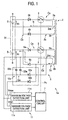
- a voltage equalizer 1a according to a first embodiment of the inventionwill be described, the first embodiment constituting a base mode for carrying out the invention.
- reference numeral 31 denotes a battery, in particular, a battery that is installed in electric vehicles run by motors and hybrid vehicles run by using engines in combination with motors.
- This battery 31 is such as to be made up of a plurality of battery elements B ... which are connected in series, and various types of battery elements including ion batteries such as lithium ion batteries and electric double layer capacitors can be used for the battery elements B... .
- each battery element B may be made up of a single cell or a plurality of cells, which are connected in series, in parallel, or in combination thereof.
- a voltage equalizer 1a for equalizing terminal voltages Vo... of the respective battery elements B... is connected to the battery 31.
- the voltage equalizer 1a includes a transformer 2 having an iron core.
- the transformer 2 has a plurality of basic windings 2o... which are provided in such a manner as to correspond, respectively, to the battery elements B... .
- each basic winding 2o has a primary winding 2a and a secondary winding 2b which are separated by a center tap (an intermediate tap) 2oc, and the center tap 2oc is connected to a negative pole side of the corresponding battery element B.
- numbers of turns of the respective basic windings 2o... are set to be the same.
- the primary windings 2a... and the secondary windings 2b... in the first embodiment have the same number of turns.
- center tap 2oc functions a winding termination terminal of the secondary winding 2b as well as a winding initiation terminal of the primary winding 2a.
- a series circuit of a switching element 3 and a primary diode (a one-way conductor element) 5a is connected between a winding termination terminal of the primary winding 2a and a positive pole side of the corresponding battery element B, and a winding initiation terminal of the secondary winding 2b is connected to the positive pole side of the corresponding battery element B via a secondary diode (a one-way conductor element) 5b, whereby a plurality of primary series circuits Ca...
- reference numeral 7 denotes a control circuit.
- the control circuit 7 outputs a pulse control signal Ps which is oscillated from a pulse oscillator installed therein and whose frequency is in the order of a hundred kHz, and the respective switching elements 3... are ON/OFF controlled in a synchronized fashion by this pulse control signal Ps.
- a voltage detection circuit 11 is connected to the equalization processing circuit 6 for detecting a maximum terminal voltage Vmax and a minimum terminal voltage Vmin in the respective (all) battery elements B... .
- the voltage detection circuit 11 includes a maximum voltage detection unit 11m and a minimum voltage detection unit 11s, and a winding termination terminal of the primary winding 2a of any basic winding 2o is connected to one of input ports of the maximum voltage detection unit 11m via a diode 32, and a center tap 2oc of the relevant basic winding 2oc is connected to the other input port of the maximum voltage detection unit 11m.
- a winding termination terminal of the secondary winding 2b of the basic winding 2o is connected to one of input ports of the minimum voltage detection unit 11s via a diode 32b, and a center tap 2oc of the basic winding 2o is connected to the other input port of the minimum voltage detection unit 11s.
- a voltage holding capacitor 33a is connected between an output side of the diode 32a and the center tap 2oc, and a voltage holding capacitor 33b is connected between an output side of the diode 32b and the center tap 2oc.
- the diode 32a and the voltage holding capacitor 33a constitute a maximum voltage holding circuit 12m for holding (storing) a maximum terminal voltage Vmax
- the diode 32b and the voltage holding capacitor 33b constitute a minimum voltage holding circuit 12s for holding (storing) a minimum terminal voltage Vmin.
- pulse signals Ps are given to the respective switching elements 3... by the control circuit 7, and the switching elements 3... are ON/OFF controlled while being synchronized with the pulse control signals Ps so given to them.
- An ON/OFF condition (pulse control signal Ps) of the switching elements 3... is shown in Fig. 5A.
- step S1 An equivalent circuit Ua of the voltage equalizer 1a when the respective switching elements 3... are switched on is shown in Fig. 3.
- the plurality of primary series circuits Ca... are configured in each of which current is carried from the battery element B to the primary winding 2a via the corresponding diode 5a, and the respective primary circuits Ca... so configuredare connected in parallel with each other.
- a storage current Is flows from the battery element B in all of the battery elements B...
- step S2 Since energy is stored in the transformer 2 through the flow of the storage current Is only from the battery element B having the maximum terminal voltage Vomax, an equalization process is performed to reduce the maximum terminal voltage Vomax of the relevant battery element B (step S2).
- the maximum terminal voltage Vmax that is generated at both terminals (a winding initiation terminal and a winding termination terminal) of the primary winding 2a is held (stored) by the maximum voltage holding circuit 12m. Namely, the maximum terminal voltage Vmax is supplied to the voltage holding capacitor 33a via the diode 32a and is held as the terminal voltage of the voltage holding capacitor 33a (step S3).
- the storage current Is increases gradually from the point in time when the respective switching elements 3... are switched on. Due to this, the terminal voltage Va of the primary winding 2a and the maximum terminal voltage Vmax which is an output from the diode 32a become as shown in Fig.
- step S4 An equivalent circuit Ub of the voltage equalizer 1a when the respective switching elements 3... are switched off is shown in Fig. 4.
- the plurality of secondary series circuits Cb... are configured in each of which current is carried from the secondary winding 2b to the battery element B via the secondary diode 5b, and the secondary series circuits Cb... so configured are connected in parallel with each other.
- an emission current Ir flows from the secondary winding 2b to the battery element B in all of the battery elements B...
- the minimum terminal voltage Vimin that is generated at both terminals (a winding initiation terminal and a winding termination terminal) of the secondary winding 2b is held (stored) by the minimum voltage holding circuit 12s.
- the minimum terminal voltage Vmin is supplied to the voltage holding capacitor 33b via the diode 32b and is held as the terminal voltage of the voltage holding capacitor 33b (step S6).
- the emission current Ir decreases gradually from the point in time when the respective switching elements 3... are switched off. Due to this, the terminal voltage Vb of the secondary winding 2b and the minimum terminal voltage Vmin which is an output from the diode 32b become as shown in Fig.
- the voltage equalization process is implemented on the respective battery elements B... by repeating the ON/OFF operations of the switching elements 3... , and in the end, the terminal voltages Vo of all the battery elements B... are equalized.
- the equalization processing circuit 6 since, when the respective switching elements 3... are switched on, the storage currents Is... generated in association with the storage of energy into the transformer 2 are caused to flow from the battery elements B... having the maximum terminal voltage Vomax to the basic windings 2o... , whereas, when the respective switching elements 3... are switched off, the emission currents Ir... generated in association with the emission of energy from the transformer 2 are caused to flow from the basic windings 2o... to the battery elements B...
- the equalization process can be implemented both when energy is stored into the transformer 2 and when energy is emitted from the transformer 2, whereby the equalizing ability and equalizing efficiency can be enhanced remarkably.
- the terminal voltages Vo... of the battery elements B... vary largely, since the emission currents Ir... (the storage currents Is%) flow through the secondary series circuits Cb... (the primary series circuits Ca%) individually, the generation of an adverse effect that excessive emission currents Ir... (storage currents Is%) flow when the equalizing process is being carried out can be prevented.
- step S7, S8 maximum terminal voltage Vmax and minimum terminal voltage Vmin detection processes are carried out when predetermined sampling times are reached.
- the maximum terminal voltage Vmax since the maximum terminal voltage Vmax is held in the maximum voltage holding circuit 12m (the voltage holding capacitor 33a), the maximum terminal voltage Vmax can be detected only by reading the terminal voltage of the voltage holding capacitor 33a by the maximum voltage detection unit 11m. Then, the maximum terminal voltage Vmax so detected is sent to the control circuit 7 as a datum to be stored in a memory of the control circuit 7 at least temporarily.
- the minimum terminal voltage Vmin is held in the minimum voltage holding circuit 12s (the voltage holding capacitor 33b)
- the minimum terminal voltage Vmin can be detected only by reading the terminal voltage of the voltage holding capacitor 33b by the minimum voltage detection unit 11s. Then, the minimum terminal voltage Vmin so detected is sent to the control circuit 7 to be stored in the memory of the control circuit 7 at least temporarily.
- the maximum terminal voltage Vmax and the minimum terminal voltage Vmin can easily be detected, and since the voltage detection circuit 11 also functions as a substantial part of the voltage equalizer 1a, the configuration of the voltage equalizer 1a can be attempted to be simplified. Moreover, since the necessity of a conventional detection circuit for independently detecting each of the terminal voltages Vo... of the respective battery elements B... can be obviated, when thinking of the entirety of the system, the production cost can be reduced, the energy loss can be reduced, and the size can be made compact. Since a main obj ect of the voltage detection circuit 11 is to detect the battery elements B... whose terminal voltages Vo...
- the object can be sufficiently met when only the maximum terminal voltage Vmax and the minimum terminal voltage Vmin can be detected, and therefore, there is no need to detect even normal terminal voltages Vo... Consequently, the original object can be attained to a sufficient extent in the event that the voltage detection circuit 11 according to the first embodiment is used which detects only the maximum terminal voltage Vmax and the minimum terminal voltage Vmin.
- the maximum voltage holding circuit 12m and the minimum voltage holding circuit 12s are provided in the voltage detection circuit 11, the maximum terminal voltage Vmax that is generated when the respective switching elements 3... are switched on and the minimum terminal voltage Vmin that is generated when the respective switching elements 3... are switched off can be detected without being affected by ON/OFF timings of the respective switching elements 3... .
- the detection processing system can be attempted to be simplified.
- Fig. 6 shows experimental data on maximum terminal voltages Vmax and minimum terminal voltages Vmin detected by the voltage detection circuit 11 according to the first embodiment.
- a battery 31 was used in which eight battery elements B... are connected in series.
- Vo[V] represents measured data which resulted from direct measuring of terminal voltages of the respective battery elements B... .
- an experimental result No. 1 shows a sample which includes six battery elements 2 to 7 which have average terminal voltages, one battery element 1 whose terminal voltage is relatively low and one battery element 8 whose terminal voltage is relatively high
- an experimental result No. 2 shows a sample which is a combination of battery elements 1 to 4 whose terminal voltages are relatively low and battery elements 5 to 8 whose terminal voltages are relatively high.
- a minimum terminal voltage Vmin and a maximum terminal voltage Vmax detected by the voltage detection circuit 11 were 2.034[V] and 3.970[V], respectively. Consequently, the terminal voltage of the battery element 1 which constitutes a minimum voltage was 2.003[V], and an error therefrom was 0.031[V] (1.55[%]). In addition, the terminal voltage of the battery element 8 which constitutes a maximum voltage was 4.032[V], and an error therefrom was -0.062[V] (-1.54[%]). Furthermore, in the experimental result No. 2, a minimum terminal voltage Vmin and a maximum terminal voltage Vmax detected by the voltage detection circuit 11 were 2.046[V] and 3.943[V], respectively.
- the terminal voltage of the battery element 4 which constitutes a minimum voltage was 2. 062[V], and an error therefrom was -0.016[V] (-0.78[%]).
- the terminal voltages of the battery elements 7, 8 which constitute a maximum voltage were 3.946[V], and an error therefrom was -0.003[V] (-0.08[%]).
- the data as to the maximum terminal voltage Vmax and the minimum terminal voltage Vmin which are temporarily stored in the control circuit 7 are used to set a control condition for the switching elements 3... .
- the differential voltage Ve so obtained is equal to or smaller than a set value Es which was set in advance, the ON/OFF control of the switching elements 3... is stopped, so that the switching elements 3... are in the OFF state (steps S10, S11).
- a small differential voltage Ve means that the terminal voltages Vo... of the respective battery elements B...
- step S10 when the differential voltage Ve exceeds the set value Es, the terminal voltages Vo... of the respective battery elements B... vary largely, needing an equalization process, and consequently, the ON/OFF control of the switching elements 3... is made to continue as it is (step S10).
- a switching frequency fs for ON/OFF controlling the switching elements 3... is caused to change in accordance with the magnitude of the differential voltage Ve (steps S10, S11). Namely, when the differential voltage Ve is large, a control condition changing process for setting the switching frequency fs low is performed, whereas, when the differential voltage Ve is small, a control condition changing process for setting the switching frequency fs high is performed.
- the differential voltage Ve is small, the amount of energy stored in and emitted from the transformer 2 is reduced so as to reduce a wasteful loss by reducing the time when the switching elements 3... are ON, whereas, when the differential voltage Ve is large, the capability of the equalization process can be increased by increasing the time when the switching elements 3... are ON.
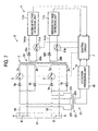
- this voltage equalizer 1b differs from the voltage equalizer 1b of the first embodiment in that a maximum terminal voltage Vmax and a minimum terminal voltage Vmin are detected by a detection winding 2d which is provided separately in the transformer 2, that a detection timing is set so that a maximum terminal voltage Vmax and a minimum terminal voltage Vmin can be detected accurately, and that a pulse control signal Ps, which performs a self-oscillation and changes its frequency in accordance with the magnitudes of storage currents Is... and emission currents Ir... , is used when ON/OFF controlling the switching elements 3.
- the voltage equalizer 1b has the detection winding 2d which is provided separately in the transformer 2 and which includes a primary detection winding 2da and a secondary detection winding 2db. Since the primary detection winding 2da is used to detect a maximum terminal voltage Vmax, a winding termination terminal thereof is connected to one of input ports of a maximum voltage detection unit 11m via a diode 32a, and a winding initiation terminal thereof is connected to the other input port of the maximum voltage detection unit 11m via a switching element 51a.
- a winding initiation terminal thereof is connected to one of input ports of a minimum voltage detection unit 11s via a diode 32b, and a winding termination terminal thereof is connected to the other input port of the minimum voltage detection unit 11s via a switching element 51b.
- the current detection unit 55 includes a detection transformer 57 having current detection windings 57f... which functions as a current transformer (CT) and a detection processing unit 58.
- the respective current detection windings 57f... connect in series between positive pole sides of respective battery elements B... and respective diodes 5a and 5b so as to detect the magnitude of emission currents Ir... which flow into the battery elements B... or storage currents Is... which flow out of the battery elements B...
- an output winding 57s of the detection transformer 57 is connected to an input side of the detection processing unit 58, an output side of the detection processing unit 58 connecting to a control circuit 7.
- like reference numerals are imparted to like portions in Fig. 7 to those shown in Fig. 1 so as not only to make clear the configuration shown in Fig. 7 but also to omit a detailed description thereof.
- the ON/OFF control of the switching elements 3... is not implemented by a pulse control signal Ps whose frequency is stationary but by a pulse control signal Ps whose frequency is variable in accordance with the magnitude of storage currents Is... and emission currents Ir... .
- This pulse signal Ps is generated as follows. Now, assume that the switching elements 3... are in the OFF state. In this case, emission currents Ir... are detected by the current detection unit 55. Since the emission currents Ir decrease gradually as shown in Fig. 5B, the control circuit 7 monitors the magnitude of emission currents Ir... which are detected and starts the ON control of the switching elements 3...
- the control circuit 7 monitors the magnitude of the storage currents Is... so detected and starts the OFF control of the switching elements 3... at a timing when the storage currents Is... have reached a predetermined value Ism.
- control circuit 7 starts self-oscillation, and therefore, a separate oscillator which oscillates a stationary switching frequency (ON/OFF frequency) fs is no more required.
- a stationary switching frequency ON/OFF frequency
- Is ... stable storage currents
- no-current time period can be eliminated, so that a voltage equalizing process can be performed efficiently. Due to this, it is desirable to set the length of the predetermined time Tr and the magnitude of the predetermined value Ism so as to obtain those effects.
- the control circuit 7 starts the ON control of the switch element 51a in the voltage detection circuit 11 at a timing when a predetermined time Td, which is set in advance, has elapsed since the switching elements 3... were switched on and performs a process in which a maximum terminal voltage Vmax is detected by the maximum voltage detection unit 11m.
- the switching element 51a is ON controlled only when the maximum terminal voltage Vmax is detected, whereby since an error that would be generated by the voltage drops by the primary diodes 5a... can be ignored and the maximum terminal voltage Vmax can be detected at a constant detection timing at all times, a maximum terminal voltage Vmax which is free from variation and is accurate can be detected.
- the control circuit 7 monitors the magnitude of the emission currents Ir... after the switching elements 3... have been switched off and starts the ON control of the switching element 51b in the voltage detection circuit 11 at a timing (a point ts in Fig. 5B) when a predetermined threshold Irs has been reached, a process being carried out in which a maximum terminal voltage Vmin is detected by the minimum voltage detection unit 11s.
- the switching element 51b is ON controlled only when the maximum terminal voltage Vmin is detected, whereby since not only can an error by the voltage drop by the secondary diodes 5b... be ignored, but also the minimum terminal voltage Vmin can be detected at a constant detection timing at all times, a minimum terminal voltage Vmin which is free from variation and is accurate can be detected. Note that the detection of maximum terminal voltage Vmax and minimum terminal voltage Vmin at the set detection timings can equally be implemented even when a pulse oscillator is used which oscillates a stationary switching frequency (ON/OFF frequency) fs.
- the detection of a minimum terminal voltage Vmin can also be carried out in the following manner. Namely, the minimum voltage detection unit 11s obtains in advance through an operation a predetermined time Ts that is spent the magnitude of emission currents Ir... generated in association with the emission of energy from the transformer 2 decreases to a predetermined threshold Irs and can detect a minimum terminal voltage Vmin at a timing when the predetermined time Ts has elapsed since the switching elements 3... were switched off. This obviates the necessity of detection of emission currents Ir... , thereby making it possible to attempt to simplify the detection processing system.
- This voltage equalizer 1c differs from the voltage equalizer 1a of the first embodiment in that primary windings 2a... and secondary windings 2b... are made up of windings which are completely separated, that a winding having a center tap is used for a separate winding 2d provided in a voltage detection circuit 11, and that a correction circuit 13 is provided.
- the voltage detection circuit 11 utilizes the separate detection winding 2d shown in Fig. 7, the maximum voltage holding circuit 12m and the minimum voltage holding circuit 12s which are shown in Fig. 1 are combined, and a correction circuit 13 is provided for correcting a voltage detected from the terminal voltage of the detection winding 2d.
- the correction circuit 13 is such as to construct a closed circuit by connecting a diode 64, a resistor 65 and diodes 66 and 67 in series to a correction winding 63.
- reference numeral 68 denotes a capacitor
- reference numerals 61a, 61b denote, respectively, resistors which are connected in parallel to the voltage holding capacitors 33a, 33b. While the embodiment is described as the maximum terminal voltage Vmax being corrected, a correction circuit for correcting a minimum terminal voltage can equally be provided. Alternatively, a similar correction to the correction implemented by the correction circuit 13 may be implemented using a digital processing function performed in a voltage detection unit 11c. Note that both the maximum voltage detection unit 11m and the minimum voltage detection unit 11s are contained in the voltage detection unit 11c. In addition, in Fig. 8, a path along which storage current Ir flows when switching elements 3...
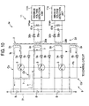
- This voltage equalizer 1d differs from the voltage equalizer 1a of the first embodiment in that basic windings 2o... are made up of single windings and are used both for primary series circuits Ca... in corresponding battery elements B... and secondary series circuits Cb... in other battery elements B... , and that an auxiliary winding 2x is provided in a transformer 2, so that the auxiliary winding 2x so provided is used as a secondary series circuit Cb in the battery element B in which a secondary series circuit Cb is not configured depending on the basic winding 2o.
- a secondary winding 2db in Fig. 9 is intended to detect a minimum terminal voltage Vmin.
- This voltage equalizer 1e is a modification made to the voltage equalizer 1d of the fourth embodiment and differs from the voltage equalizer 1d in that locations where respective components are connected are modified and that a detection winding 2d is made up of a separate winding. Consequently, the secondary winding 2db for detecting the minimum terminal voltage Vmin shown in Fig. 9 can be eliminated, whereby, when switching elements 3... are switched on, storage currents Is... flow along a path indicated by an arrow followed by a chain line in Fig. 10, whereas, when the switching elements 3... are switched off, emission currents Ir...
- the voltage equalizer 1f differs from the voltage equalizer 1d according to the fourth embodiment in that an energy replenishment circuit 22 and an energy discharge circuit 26 are provided.
- the voltage equalizer 1f includes the energy replenishment circuit 22 which conf igures a closed circuit by connecting in series a replenishment winding 2s provided in a transformer 2 for replenishing energy, a battery unit Bs for replenishing the replenishment winding 2s with energy and a replenishment switching unit 21. In this case, assuming that a maximum terminal voltage of battery elements B...
- a control circuit 7 is provided for ON/OFF controlling switching elements 3... and the replenishment switching unit 21 while causing them to synchronize with each other or ON/OFF controlling the replenishment switching unit 21 with all of the switching elements 3... being OFF controlled. Note that while being omitted from the figure, as a voltage detection circuit 11, the voltage detection circuit 11 shown in Fig. 10 can be provided.
- the energy replenishment circuit 22 remains a source from which the maximum terminal voltage Vomax is generated at all times, whereby storage current Is flows along a path indicated by an arrow followed by a chain line.
- the battery unit Bs can replenish the battery elements B... with energy, whereby an excessive self-discharge in the battery elements B... can be avoided.
- the voltage equalizer 1f includes the energy discharge circuit 26 which configures a closed circuit by connecting in series a discharge winding 2r provided in the transformer 2 for discharging energy, the battery unit Bs which is charged with energy discharged from the discharge winding 2r, a diode 62 and a discharge switching unit 25.
- the control circuit 7 is provided for ON/OFF controlling the switching elements 3... and the discharge switching unit 25 while causing them to synchronize with each other in a reversed state or ON/OFF controlling the switching elements 3... with the discharge switching unit 25 being ON controlled.
- the energy discharge circuit 26 remains a source from which the minimum terminal voltage Vomin is generated at all times, whereby emission currents Ir... flow along a path indicated by an arrow followed by a chain line.
- the battery unit Bs can be charged with energy of the battery elements B... , whereby an excessive charging of the battery elements B... can be avoided.
- the equalization processing circuit in the voltage equalizer 1d shown in Fig. 9 is configured as a single module M, and a plurality of battery elements B... which correspond to a plurality of modules M... are connected in parallel to each other.
- a primary winding 2da and a secondary winding 2db which constitute a voltage detection circuit 11 are connected in parallel to each other, and diodes 32a, 32b and voltage holding capacitors 33a, 33b are connected to the modules M... in such a manner as to be used equally by the modules M... .
- the equalization processing circuit 6 By configuring the equalization processing circuit 6 as a module, for example, even in the event that the size of a transformer 2 is standardized, it is possible to deal with an arbitrary number of different battery elements B... in a proper fashion. Then, the voltage equalization process can be implemented as when the module M is used singly, and the voltage detection by the voltage detection circuit 11 can be implemented. Note that additionally, in Fig. 12, like reference numerals are imparted to like portions to those shown in Fig. 9 so as not only to make clear the configuration shown in Fig. 12 but also to omit a detailed description thereof.
- the equalization processing circuit 6 can be configured as a single module which has a transformer 2 having, in turn, a plurality of basic windings 2o... which correspond, respectively, to battery elements B... , a plurality of switching elements 3... which correspond, respectively, to the battery elements B... , and a plurality of sets of primary diodes 5a... and secondary diodes 5b to thereby configure a plurality of primary series circuits Ca... in which current is carried from the respective battery elements B... via the corresponding primary diodes 5a...
- the equalization processing circuit 6 in the voltage equalizer 1f according to the sixth embodiment shown in Fig. 11 is configured as a single module, and a plurality of battery elements B... which correspond, respectively, to a plurality of modules M... are connected in series to each other.
- a common single battery unit Bs can be utilized, and a secondary diode 5b in any module M can be connected to an adjacent following module M.
- a voltage detection circuit 11 is omitted from Fig. 13, a voltage detection circuit 11 can be provided as in the case shown in Fig. 12.
- the module M so configured can equally be applied.
- the voltage equalizer 1h as in the case with the voltage equalizer 1g, it is possible to deal with an arbitrary number of different battery elements B... in a proper fashion.
- a voltage equalization process can be implemented as when the module M is used singly, and the voltage detection by the voltage detection circuit 11 can be implemented.
- like reference numerals are imparted to like portions to those shown in Fig. 11 so as not only to make clear the configuration shown in Fig. 13 but also to omit a detailed description thereof.
- a minimum voltage detection unit 11sg (11sga, 11sgb) is provided for detecting a minimum end-to-end voltage of end-to-end voltages of respective groups G... of one or two or more groups which result when a plurality of battery elements B... are so grouped.
- various types of battery elements including ionbatteries such as lithium ion batteries and electric double layer capacitors exist for use as the battery element B.
- ion batteries in the event that the terminal voltage Vo decreases below the normal voltage, an excessive discharge is called for, and this constitutes a cause for the failure of a battery.
- capacitors such as electric double layer capacitors
- capacitors even in the event that the terminal voltage Vo decreases below the normal voltage, there is no case where a problem (abnormality) is caused. Consequently, with capacitors such as electric double layer capacitors, it is not necessary to know accurately the minimum terminal voltages Vomin... of the individual battery elements B... , but it is sufficient to obtain information on whether or not there is occurring a failure, and there is a case where the information itself is not actually needed.
- aminimumend-to-endvoltage Vxmin of end-to-end terminal voltages of respective groups G... of one or two or more groups resulting when a plurality of battery elements B... are so grouped is designed to be detected by a minimum voltage detection unit 11sg.
- basic windings 2o ... are each made up of a plurality of primary windings 2a... which correspond, respectively, to battery elements B... and one or two or more secondary windings 2b... which correspond, respectively, to groups G... of one or two or more groups which result when the plurality of battery elements B ...
- the minimumend-to-endvoltages Vxmin... so obtained can be used to anticipate the existence of battery elements B... in which something abnormal is being caused and to control the charging and discharging of the whole battery 31.
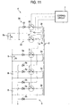
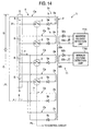
- the voltage equalizer 1i according to the ninth embodiment of the invention will be described below.
- this voltage equalizer as an example, there are provided four primary windings 2a... and two secondary windings 2b, which is a half of the primary windings 2a...
- basic windings 2o... has four primary windings 2a... which correspond, respectively, to four battery elements B... , which are grouped into two groups G... of two battery elements, and two secondary windings 2b... which correspond, respectively, to the groups G....
- primary series circuits Ca... function in a similar way to that in which those of the voltage equalizer 1a according to the first embodiment do.
- the voltage equalizer 1j according to the tenth embodiment of the invention will be described below.
- this voltage equalizer 1j as an example, five primary windings 2a... are provided, and two of the five are also used as secondary windings 2b... .
- the two primary windings 2a... to which secondary diodes 5b... are connected are also used as the secondary windings 2b...
- two battery elements B... constitute a group G.
- primary series circuits Ca... function in a similar way to that in which those of the voltage equalizer 1a according to the first embodiment do. Namely, when respective switching elements 3...
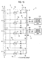
- the voltage equalizer 1k according to the eleventh embodiment of the invention will be described below.
- a single secondary winding 2b is provided, while a plurality of primary windings 2a... are provided. Due to this, basic windings 2o have a plurality of primary windings 2a... which correspond, respectively, to battery elements B... , and all of the battery elements B... are grouped into a single group G.
- primary series circuits Ca... function in a similar way to that in which those of the voltage equalizer 1a according to the first embodiment do. Namely, when respective switching elements 3...
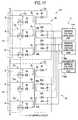
- the voltage equalizer 1m according to the twelfth embodiment of the invention will be described below.
- the voltage equalizer 1k according to the eleventh embodiment is configured into a single module M, and a plurality of (two in the embodiment) models M... are connected in series. Consequently, the function (operation) of each of the modules M... becomes identical with that of the voltage equalizer 1k according to the eleventh embodiment.
- terminal voltages of battery elements B... of all the modules M... are equalized in a similar way to that in which the terminal voltages of the battery elements are equalized by the voltage equalizer 1k in the eleventh embodiment.
- a maximum voltage detection unit 11m, a minimum voltage detection unit 11sga and a secondary minimum voltage detection unit 11sgb are connected as shown in Fig. 17, whereby a maximum terminal voltage Vomax of the respective battery elements B... in all the modules M... can be detected in the maximum voltage detection unit 11m, the end-to-end voltage of a battery 31 in one (upper one in the figure) of the modules M can be detected by the primary minimum voltage detection unit 11sga, and the end-to-end voltage of all the modules M... which results from the addition of the end-to-end voltage of the upper module M and the end-to-end voltage of the lower module M can be detected by the secondary minimum voltage detection unit 11sgb.
Landscapes
- Engineering & Computer Science (AREA)
- Power Engineering (AREA)
- Life Sciences & Earth Sciences (AREA)
- Sustainable Development (AREA)
- Sustainable Energy (AREA)
- Transportation (AREA)
- Mechanical Engineering (AREA)
- Charge And Discharge Circuits For Batteries Or The Like (AREA)
- Secondary Cells (AREA)
- Electric Propulsion And Braking For Vehicles (AREA)
Applications Claiming Priority (4)
| Application Number | Priority Date | Filing Date | Title |
|---|---|---|---|
| JP2003435418 | 2003-12-26 | ||
| JP2003435418 | 2003-12-26 | ||
| JP2004101118 | 2004-03-30 | ||
| JP2004101118A JP3795499B2 (ja) | 2003-12-26 | 2004-03-30 | 蓄電素子の電圧均等化装置 |
Publications (2)
| Publication Number | Publication Date |
|---|---|
| EP1575143A2 true EP1575143A2 (de) | 2005-09-14 |
| EP1575143A3 EP1575143A3 (de) | 2007-08-01 |
Family
ID=34703342
Family Applications (1)
| Application Number | Title | Priority Date | Filing Date |
|---|---|---|---|
| EP04030303A Withdrawn EP1575143A3 (de) | 2003-12-26 | 2004-12-21 | Spannungsausgleichsschaltung für Batteriezellen |
Country Status (3)
| Country | Link |
|---|---|
| US (1) | US7400114B2 (de) |
| EP (1) | EP1575143A3 (de) |
| JP (1) | JP3795499B2 (de) |
Cited By (1)
| Publication number | Priority date | Publication date | Assignee | Title |
|---|---|---|---|---|
| EP2843796A1 (de) * | 2013-08-27 | 2015-03-04 | General Electric Company | Batteriemanagementsystem und entsprechendes Verfahren |
Families Citing this family (39)
| Publication number | Priority date | Publication date | Assignee | Title |
|---|---|---|---|---|
| KR101124725B1 (ko) * | 2006-06-15 | 2012-03-23 | 한국과학기술원 | 전하 균일 장치 |
| US8692515B2 (en) * | 2006-06-22 | 2014-04-08 | Fdk Corporation | Series-connected rechargeable cells, series-connected rechargeable cell device, voltage-balance correcting circuit for series-connected cells |
| JP4734268B2 (ja) * | 2007-02-13 | 2011-07-27 | プライムアースEvエナジー株式会社 | 放電システム、および電動車両 |
| JP5517398B2 (ja) * | 2007-03-15 | 2014-06-11 | 三菱重工業株式会社 | 蓄電システム |
| EP2249453B1 (de) * | 2008-01-07 | 2018-04-25 | Panasonic Intellectual Property Management Co., Ltd. | Stromakkumulationsvorrichtung |
| KR101011235B1 (ko) * | 2008-10-27 | 2011-01-26 | 킴스테크날리지 주식회사 | 전기에너지 저장장치의 전압균등화회로 |
| US9397508B2 (en) * | 2009-05-22 | 2016-07-19 | Intersil Americas LLC | System and method for cell balancing and charging using a serially coupled inductor and capacitor |
| US8541980B2 (en) * | 2009-05-22 | 2013-09-24 | Intersil Americas LLC | System and method for cell balancing and charging |
| TWI400854B (zh) * | 2009-09-15 | 2013-07-01 | 登豐微電子股份有限公司 | 電池電壓平衡電路及方法 |
| US8339100B2 (en) * | 2009-09-29 | 2012-12-25 | O2Micro Inc | Systems and methods for cell balancing |
| CN102035010B (zh) | 2009-09-29 | 2013-05-01 | 凹凸电子(武汉)有限公司 | 电池单元均衡电路及方法 |
| CN102823104B (zh) * | 2010-02-05 | 2016-05-11 | 法国原子能源和替代能源委员会 | 用于电池的充电均衡系统 |
| FR2959885B1 (fr) * | 2010-05-05 | 2014-12-05 | Commissariat Energie Atomique | Systeme d'equilibrage pour batterie de puissance, procede d'equilibrage de charge et procede combine d'equilibrage de charge et d'alimentation correspondants |
| DE102010029460A1 (de) * | 2010-05-28 | 2011-12-01 | Siemens Aktiengesellschaft | Symmetriereinrichtung und Symmetrierverfahren |
| US8436582B2 (en) * | 2010-07-09 | 2013-05-07 | Freescale Semiconductor, Inc. | Battery cell equalizer system |
| US8773068B2 (en) * | 2011-01-20 | 2014-07-08 | Valence Technology, Inc. | Rechargeable battery systems and rechargeable battery system operational methods |
| US8957624B2 (en) | 2011-01-20 | 2015-02-17 | Valence Technology, Inc. | Rechargeable battery systems and rechargeable battery system operational methods |
| US8922167B2 (en) | 2011-01-20 | 2014-12-30 | Valence Technology, Inc. | Rechargeable battery systems and rechargeable battery system operational methods |
| DE102011009474A1 (de) * | 2011-01-26 | 2012-07-26 | Liebherr-Elektronik Gmbh | Vorrichtung und Verfahren zum Überwachen und Symmetrieren eines mehrzelligen Energiespeicherstapels |
| CN102738843A (zh) * | 2011-04-07 | 2012-10-17 | 美律实业股份有限公司 | 电池串联能量平衡电路 |
| US9209630B2 (en) * | 2011-05-20 | 2015-12-08 | Ford Global Technologies, Llc | Active battery cell balancing methods with variable duration discharge |
| US9166419B2 (en) * | 2011-10-31 | 2015-10-20 | Robert Bosch Gmbh | Intelligent charging and discharging system for parallel configuration of series cells with semiconductor switching |
| EP2816701B1 (de) * | 2012-02-16 | 2018-05-02 | Nec Corporation | Einstellvorrichtung, batterieanordnung und einstellverfahren |
| FR2998728B1 (fr) * | 2012-11-23 | 2015-12-25 | Renault Sas | Systeme d'equilibrage d'une batterie de traction d'un vehicule |
| JP5815010B2 (ja) * | 2013-11-19 | 2015-11-17 | 蔡富生 | バッテリーユニットのバランシングのためのバランシング回路 |
| US9673658B2 (en) * | 2014-03-06 | 2017-06-06 | Samsung Electro-Mechanics Co., Ltd. | Non-contact capacitive coupling type power charging apparatus and non-contact capacitive coupling type battery apparatus |
| CN106663953B (zh) * | 2014-07-17 | 2019-07-26 | 贝能思科技有限公司 | 用于均衡由n个电能单位串联成一串的装置及其制造方法 |
| US9537329B2 (en) | 2014-08-29 | 2017-01-03 | General Electronics Applications, Inc. | Battery management circuit maintaining cell voltages between a minimum and a maximum during charging and discharging |
| US9819208B2 (en) | 2014-08-29 | 2017-11-14 | General Electronics Applications, Inc. | Battery management circuit having cell connections for batteries and a plurality of corresponding windings and diodes |
| TWI581543B (zh) * | 2014-10-03 | 2017-05-01 | 輝創電子股份有限公司 | 串聯電池組的主動平衡模組及其控制方法 |
| CN109429540A (zh) * | 2016-04-18 | 2019-03-05 | 莱恩半导体股份有限公司 | 用于可重配置的dickson star开关式电容器电压调节器的装置、系统和方法 |
| JP6741945B2 (ja) * | 2016-09-13 | 2020-08-19 | ミツミ電機株式会社 | 電池制御回路 |
| USRE50103E1 (en) | 2017-04-14 | 2024-08-27 | Lion Semiconductor Inc. | Circuits for a hybrid switched capacitor converter |
| US11876394B2 (en) | 2017-12-21 | 2024-01-16 | Eric Paul Grasshoff | Active cell balancing in batteries using switch mode dividers |
| US10910847B2 (en) | 2017-12-21 | 2021-02-02 | Eric Paul Grasshoff | Active cell balancing in batteries using switch mode dividers |
| CN109037814B (zh) * | 2018-09-05 | 2021-02-19 | 成都芯源系统有限公司 | 一种充电平衡管理电路和方法 |
| US11239670B2 (en) * | 2018-09-16 | 2022-02-01 | Richard Landry Gray | Cell balancing battery module and electrical apparatus |
| JP7185676B2 (ja) * | 2020-10-27 | 2022-12-07 | アオイ電子株式会社 | 半導体リレー装置 |
| US12352788B2 (en) * | 2021-04-29 | 2025-07-08 | GM Global Technology Operations LLC | Thermal runaway prognosis by detecting abnormal cell voltage and SOC degeneration |
Family Cites Families (26)
| Publication number | Priority date | Publication date | Assignee | Title |
|---|---|---|---|---|
| US3897591A (en) * | 1942-08-27 | 1975-07-29 | Bell Telephone Labor Inc | Secret transmission of intelligence |
| JPS50497Y1 (de) * | 1970-08-13 | 1975-01-09 | ||
| US4079303A (en) * | 1976-07-28 | 1978-03-14 | The United States Of America As Represented By The United States Department Of Energy | Charging system and method for multicell storage batteries |
| US4331911A (en) * | 1978-05-22 | 1982-05-25 | Park Robert H | Method of equalizing the voltages of the individual cells of storage batteries |
| US4210779A (en) * | 1978-08-11 | 1980-07-01 | Tii Corporation | Amplitude modulated telephone carrier system and terminal equipment therefor |
| FR2547106B1 (fr) * | 1983-05-30 | 1985-07-12 | Cem Comp Electro Mec | Dispositif d'equilibrage d'interrupteurs connectes en serie |
| US5003244A (en) * | 1989-05-09 | 1991-03-26 | Digital Equipment Corporation | Battery charger for charging a plurality of batteries |
| JPH06209569A (ja) * | 1993-01-05 | 1994-07-26 | Yokogawa Electric Corp | スイッチング電源装置 |
| US5570276A (en) * | 1993-11-15 | 1996-10-29 | Optimun Power Conversion, Inc. | Switching converter with open-loop input voltage regulation on primary side and closed-loop load regulation on secondary side |
| DE4428769C1 (de) * | 1994-08-13 | 1996-05-02 | Fraunhofer Ges Forschung | Vorrichtung zur Aufladung von und/oder zum Ladungsaustausch zwischen einer Vielzahl von in Reihe geschalteten Energiespeichern |
| US5659237A (en) * | 1995-09-28 | 1997-08-19 | Wisconsin Alumni Research Foundation | Battery charging using a transformer with a single primary winding and plural secondary windings |
| US5666041A (en) * | 1996-08-27 | 1997-09-09 | The University Of Toledo | Battery equalization circuit with ramp converter |
| US5982143A (en) * | 1996-08-27 | 1999-11-09 | The University Of Toledo | Battery equalization circuit with ramp converter and selective outputs |
| DE29901322U1 (de) * | 1999-01-28 | 1999-07-08 | Melcher Ag, Uster | Spannungskonverter |
| JP2001128387A (ja) * | 1999-10-28 | 2001-05-11 | Nagano Japan Radio Co | 充電装置 |
| US6222344B1 (en) * | 1999-12-06 | 2001-04-24 | Bae Systems Controls, Inc. | Magnetically coupled autonomous battery equalization circuit |
| JP3364836B2 (ja) * | 2000-10-19 | 2003-01-08 | 富士重工業株式会社 | 電圧イコライザ装置およびその方法 |
| JP3630303B2 (ja) | 2000-11-21 | 2005-03-16 | 長野日本無線株式会社 | 蓄電素子の電圧均等化装置 |
| US6373223B1 (en) * | 2000-11-21 | 2002-04-16 | Nagano Japan Radio Co., Ltd. | Voltage equalizing apparatus and voltage equalizing method for battery devices |
| US6642693B2 (en) * | 2000-11-21 | 2003-11-04 | Nagano Japan Radio Co., Ltd. | Voltage equalizing apparatus for battery devices |
| JP4320511B2 (ja) * | 2001-02-19 | 2009-08-26 | 三菱電機株式会社 | 電源装置 |
| US6801014B1 (en) * | 2001-05-08 | 2004-10-05 | Arris International, Inc. | Battery equalizer using total string current |
| JP2002357625A (ja) | 2001-05-31 | 2002-12-13 | Nagano Japan Radio Co | 蓄電素子の電圧検出回路 |
| JP2003333762A (ja) * | 2002-05-14 | 2003-11-21 | Japan Storage Battery Co Ltd | 組電池用の電圧レベル均等化装置 |
| JP2004079191A (ja) * | 2002-08-09 | 2004-03-11 | Toyota Motor Corp | バッテリ充電制御装置 |
| JP2006166615A (ja) * | 2004-12-08 | 2006-06-22 | Fuji Heavy Ind Ltd | 蓄電デバイスの電圧均等化制御システム |
-
2004
- 2004-03-30 JP JP2004101118A patent/JP3795499B2/ja not_active Expired - Fee Related
- 2004-12-21 EP EP04030303A patent/EP1575143A3/de not_active Withdrawn
- 2004-12-22 US US11/021,018 patent/US7400114B2/en not_active Expired - Fee Related
Cited By (2)
| Publication number | Priority date | Publication date | Assignee | Title |
|---|---|---|---|---|
| EP2843796A1 (de) * | 2013-08-27 | 2015-03-04 | General Electric Company | Batteriemanagementsystem und entsprechendes Verfahren |
| CN104426175A (zh) * | 2013-08-27 | 2015-03-18 | 通用电气公司 | 电池管理系统和方法 |
Also Published As
| Publication number | Publication date |
|---|---|
| US7400114B2 (en) | 2008-07-15 |
| US20050140336A1 (en) | 2005-06-30 |
| JP2005210877A (ja) | 2005-08-04 |
| EP1575143A3 (de) | 2007-08-01 |
| JP3795499B2 (ja) | 2006-07-12 |
Similar Documents
| Publication | Publication Date | Title |
|---|---|---|
| EP1575143A2 (de) | Spannungsausgleichsschaltung für Batteriezellen | |
| JP5060857B2 (ja) | セルコントローラ | |
| JP3858893B2 (ja) | 電圧バランス回路、電圧検出用回路、電圧バランス方法及び電圧検出方法 | |
| JP4186916B2 (ja) | 組電池管理装置 | |
| JP3615507B2 (ja) | 組電池の充電率調整回路 | |
| US7443138B2 (en) | Battery control device for equalization of cell voltages | |
| CN113437770A (zh) | 电池充放电装置及方法 | |
| US20100019724A1 (en) | Battery system using secondary battery | |
| JP2009071936A (ja) | 組電池の電圧均等化システム | |
| Dam et al. | Low-frequency selection switch based cell-to-cell battery voltage equalizer with reduced switch count | |
| JP2001178008A (ja) | セルバランス調整回路、セル電圧異常検出回路、セルバランス調整方法およびセル電圧異常検出方法 | |
| US7531987B2 (en) | Capacitor control system | |
| KR20180072353A (ko) | 배터리 팩 | |
| US20040212352A1 (en) | Voltage equalizer for capacitors | |
| JPH11262188A (ja) | 直列組電池のばらつき補正装置及び方法 | |
| EP2320536A1 (de) | Elektroenergie-Speichermodulsteuervorrichtung | |
| JP3458740B2 (ja) | 組電池の充電装置および放電装置 | |
| Manjunath et al. | A modularized two-stage active cell balancing circuit for series connected Li-ion battery packs | |
| KR20120112072A (ko) | 보조 배터리 충전 장치 | |
| JP2006352950A (ja) | 電源装置 | |
| JP2004222438A (ja) | 電気二重層キャパシタの電圧バランス均等化回路 | |
| JP4207408B2 (ja) | 充電状態調整装置及び充電状態検出装置 | |
| JP2008079364A (ja) | 充放電装置 | |
| JP2002142375A (ja) | 蓄電装置およびその制御方法 | |
| JP7418457B2 (ja) | エネルギ移動回路、及び蓄電システム |
Legal Events
| Date | Code | Title | Description |
|---|---|---|---|
| PUAI | Public reference made under article 153(3) epc to a published international application that has entered the european phase |
Free format text: ORIGINAL CODE: 0009012 |
|
| AK | Designated contracting states |
Kind code of ref document: A2 Designated state(s): AT BE BG CH CY CZ DE DK EE ES FI FR GB GR HU IE IS IT LI LT LU MC NL PL PT RO SE SI SK TR |
|
| AX | Request for extension of the european patent |
Extension state: AL BA HR LV MK YU |
|
| PUAL | Search report despatched |
Free format text: ORIGINAL CODE: 0009013 |
|
| AK | Designated contracting states |
Kind code of ref document: A3 Designated state(s): AT BE BG CH CY CZ DE DK EE ES FI FR GB GR HU IE IS IT LI LT LU MC NL PL PT RO SE SI SK TR |
|
| AX | Request for extension of the european patent |
Extension state: AL BA HR LV MK YU |
|
| 17P | Request for examination filed |
Effective date: 20070921 |
|
| AKX | Designation fees paid |
Designated state(s): DE FR |
|
| STAA | Information on the status of an ep patent application or granted ep patent |
Free format text: STATUS: THE APPLICATION HAS BEEN WITHDRAWN |
|
| 18W | Application withdrawn |
Effective date: 20131009 |