EP1569332A1 - Leistungsverstärker und Operationsverstärker, der diesen beinhaltet - Google Patents
Leistungsverstärker und Operationsverstärker, der diesen beinhaltet Download PDFInfo
- Publication number
- EP1569332A1 EP1569332A1 EP05290377A EP05290377A EP1569332A1 EP 1569332 A1 EP1569332 A1 EP 1569332A1 EP 05290377 A EP05290377 A EP 05290377A EP 05290377 A EP05290377 A EP 05290377A EP 1569332 A1 EP1569332 A1 EP 1569332A1
- Authority
- EP
- European Patent Office
- Prior art keywords
- transistors
- transistor
- circuit
- electrodes
- main
- Prior art date
- Legal status (The legal status is an assumption and is not a legal conclusion. Google has not performed a legal analysis and makes no representation as to the accuracy of the status listed.)
- Granted
Links
Images
Classifications
-
- H—ELECTRICITY
- H03—ELECTRONIC CIRCUITRY
- H03F—AMPLIFIERS
- H03F3/00—Amplifiers with only discharge tubes or only semiconductor devices as amplifying elements
- H03F3/30—Single-ended push-pull [SEPP] amplifiers; Phase-splitters therefor
- H03F3/3069—Single-ended push-pull [SEPP] amplifiers; Phase-splitters therefor the emitters of complementary power transistors being connected to the output
-
- H—ELECTRICITY
- H03—ELECTRONIC CIRCUITRY
- H03F—AMPLIFIERS
- H03F3/00—Amplifiers with only discharge tubes or only semiconductor devices as amplifying elements
- H03F3/30—Single-ended push-pull [SEPP] amplifiers; Phase-splitters therefor
Definitions
- the present invention relates to a power amplification circuit and an operational amplifier incorporating such a circuit.
- the circuit of power amplification is used in the operational amplifier as power output stage ("output buffer").
- High input impedance, low output impedance and significant dynamics of output current and output voltage are some of the characteristics sought for an amplification circuit of power.
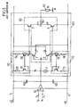
- FIG. 1 is a diagram of a differential operational amplifier, known in the prior art.
- An operational amplifier comprises two cascaded amplification stages.
- An input stage designated GM, consists of a differential transconductance amplifier 10, receiving on two positive and negative inputs respective currents Ip and In, corresponding to input electric potentials Vp and Vn.
- the transconductance amplifier 10 is connected between two voltage supply terminals, respectively a positive supply terminal 5 and a negative supply terminal 6, referenced with respect to an electric ground terminal M.
- V cc + and V cc - supply terminals 5 and 6 may be, for example, +2.5 volts and -2.5 volts.
- the currents Ip and In are of the order of a few microamperes, in absolute values.
- the electrical input potentials Vp and Vn can vary between V cc - and V cc + ; they constitute the input signals of the operational amplifier.
- the output of the transconductance amplifier 10 constitutes the output from the entrance floor. It is connected to a node A which constitutes an entry of the power output stage 100. Capacitors 102 and 103 connect the node A to the power terminals 5 and 6, respectively. They stabilize the operation of the operational amplifier.
- a node D constitutes an output of the power output stage 100, and is also an output of the operational amplifier.
- a load impedance 101 (or "load” in English), of value Z L , is connected between the node D and the ground terminal M.
- the load impedance 101 is equivalent to a resistor connected in parallel with a capacitor (not shown).
- Z L can be equal, for example, to 100 ohms in module.
- the power amplification circuit which constitutes the output stage of power 100 is hereinafter referred to as circuit 100. It comprises two circuit modules 60 and 70.
- the module 60 comprises two bipolar transistors 61 and 62 of pnp type, preferably identical to each other. Issuers transistors 61 and 62 are connected to the supply terminal 5 by resistors identical, respectively, 63 and 64, of common value R. R may be equal, for example, at 1 kilo-ohm.
- the bases of transistors 61 and 62 are connected between them, and in addition to the collector of transistor 61. In other words, the transistor 61 is diode connected.
- the module 60 thus constituted forms a Widlar current source with outgoing currents, well known. He has a operation in current mirror: the currents coming out of the collectors transistors 61 and 62 are equal to each other.
- the module 70 is also a current source Widlar, but current Incoming. It has a dual structure of that of the module 60.
- the module 70 thus comprises two bipolar transistors 71 and 72 of npn type, preferably identical to each other. Each of these transistors has a transmitter connected to the supply terminal 6 by a resistor respectively 73 and 74.
- the resistors 73 and 74 have the same common value, which can also be the R value, but not necessarily.
- the respective bases of the transistors 71 and 72 are connected together, and further to the collector of transistor 71.
- a current source 7 is connected between the collectors of the transistors 61 and 71.
- the positive terminal of the source 7 is connected to the collector of transistor 71, and the negative terminal of source 7 is connected at the collector of the transistor 61.
- the current I d current delivered by the source 7 can be, for example, 200 micro-amperes.
- the circuit 100 further comprises a module 20, of the "push-pull" type.
- the module 20 comprises two intermediate bipolar transistors 1 and 2, respectively pnp and npn.
- Transistors 1 and 2 are preferably paired, that is, they have identical structures but have different types of inverted electrical dopings with respect to each other.
- the basics of transistors 1 and 2 are connected to each other and to the node A.
- the transmitters of the transistors 1 and 2 are respectively connected to the collectors of the transistors 62 and 72, respectively by a node B and a node C.
- Transistors of 3 and 4, respectively of the npn and pnp type, preferably paired, have their bases respectively connected to the nodes B and C.
- the transmitters of the transistors 3 and 4 are connected to each other and to the node D.
- the collectors of transistors 3 and 4 are respectively connected to the power supply terminals 5 and 6.
- the collector of the transistor intermediate 1 is directly connected to the power supply terminal 6, and the collector of the intermediate transistor 2 is directly connected to the terminal power supply 5.
- V A the electrical potential of the node A
- V A is also positive and varies according to an amplification characteristic of the transconductance amplifier. 10.
- V A is equal to a saturation value which depends on V cc + .
- the transistor 1 is then in a blocked state.
- a current equal to 1 flows between the emitter and the collector of the transistor 62.
- the output current of the circuit 100 is then equal to i3-i4, where i4 is the current flowing through the transistor 4, from the emitter to the collector.
- i3 and i4 are positive.
- the value of i OUT is limited by the value of i3 given by the relation (1). This value is commonly referred to as I SOURCE . It is reached when the electric input potential Vp is greater than the electric input potential Vn, and the value of the impedance 101 is sufficiently low.
- V A When the electrical potential V A reaches a sufficiently high value, the transistor 62 is in a saturated state.
- V oh is called waste voltage, it can reach 1 volt.
- the potential V D is called the electrical output potential of the circuit 100.
- V ol A waste voltage V ol , similar to V oh , limits the value that can take the potential V D when Vp-Vn is negative. The minimum value of V D is then V cc - + V ol .
- n can be between 1 and 10.
- I CONS the total current consumed by the circuit 100. It is equal to the sum of the currents flowing respectively in the resistors 63 and 64, i2 and i3.
- I CONS (3 + n) x I. It is sought to reduce this value of the total current consumed by a power amplification circuit in the idle state.
- An object of the present invention is thus to propose a new power amplification circuit which has a reduced current consumption at the idle state, for identical SOURCE and I SINK values .
- such a circuit has waste voltages substantially equal to those of a circuit according to Figure 1.
- said third circuit module comprises fifth and sixth transistors of said second type having each a first and a second main electrode and an electrode control. Said first major electrodes of said fifth and sixth transistors are respectively connected to the second terminal voltage supply by fifth and sixth resistors substantially identical. The respective control electrodes of said fifth and sixth transistors are connected together, and the control of said fifth transistor is further connected to the second main electrode of said fifth transistor. Said second electrodes of said fifth and sixth transistors comprise respectively said first and second inputs of said third module of circuit.
- said fourth circuit module may comprise a seventh and eighth transistors of said first type, each having a first and second main electrodes and a ordered. Said first main electrodes of said seventh and eighth transistors are respectively connected to the first terminal voltage supply by seventh and eighth resistors substantially identical. The respective control electrodes of said seventh and eighth transistors are connected together, and the control of said seventh transistor is further connected to the second main electrode of said seventh transistor. Said second electrodes of said seventh and eighth transistors comprise respectively said first and second outputs of said fourth module of circuit.
- At least some of the transistors of the circuit power amplifier are bipolar transistors.
- the invention also relates to an operational amplifier comprising a power amplification circuit as described above, said circuit constituting a power output stage of said operational amplifier.
- Such an operational amplifier has a total current consumption reduced and can deliver an identical output current.
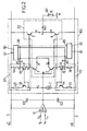
- connection between the collector of the intermediate transistor 1 and the voltage supply terminal 6, as well as the connection between the collector of the intermediate transistor 2 and the voltage supply terminal 5, are deleted. They are replaced by two circuit modules additional 80 and 90.
- the module 80 is connected to the voltage supply terminal 6 by a node 87. It is recalled that the electrical potential of the power supply terminal voltage 6 is lower than that of the voltage supply terminal 5.
- the module 80 has an input 85 connected to the collector of the transistor intermediate 1, and an input 86 connected to the emitter of the transistor 62 by a node E.
- the adopted guidelines for currents i1 and i5 are shown in FIG.
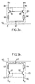
- FIG 3a is an electrical diagram of a circuit module that can be used for module 80.
- This circuit module is of type source of current Widlar to incoming currents. It includes two bipolar transistors 81 and 82 npn type.
- the emitters of transistors 81 and 82 are respectively connected to the voltage supply terminal 6 by resistors 83 and 84 substantially identical.
- the respective bases of transistors 81 and 82 are interconnected, and in addition to the collector of transistor 81.
- the Transistors 81 and 82 are preferably identical to each other.
- the resistances 83 and 84 may have a value of 1 kilo-ohm, for example.
- the module 90 is connected to the voltage supply terminal 5 by a node 97.
- the module 90 has an output 95 connected to the collector of the intermediate transistor 2, and an output 96 connected to the emitter of the transistor 72 by a node F.
- the module 90 is arranged such that a current electrical i6 flowing between the output 96 and the node F is identical to a current electrical i2 entering through the collector of transistor 2.
- i6 i2: the module 90 also has a current mirror operation.
- the orientations adopted for currents i2 and i6 are shown in FIG.
- FIG. 3b is an electrical diagram of another circuit module, which can be used for module 90.
- This other circuit module is of type Widlar current source with outgoing currents.
- Bipolar transistors 91 and 92 are of the pnp type, and are preferably identical to each other. Issuers transistors 91 and 92 are respectively connected to the power supply terminal. voltage 5 by resistors 93 and 94 substantially identical.
- the basics respective transistors 91 and 92 are connected to each other, and in addition to collector of the transistor 91.
- the resistors 93 and 94 may also have a value of 1 kilo-ohm, for example.
- denotes the absolute value. Therefore, i5 is approximately equal to 1/2. It follows that the current flowing through the transistor 62 to the quiescent state (ie when Vp Vn) is also approximately equal to l / 2. The current flowing through the transistor 62 is therefore approximately equal to half the corresponding current in the case of a circuit according to FIG.
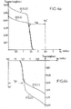
- the characteristics of a circuit 100 according to FIG. 2 are now compared with those of a circuit 100 according to FIG. 1.
- the current I of the source 7 of the circuit 100 according to FIG. 2 is adjusted. so that the two circuits have identical values of total current consumed I CONS .
- FIG. 4a illustrates the variations of I SOURCE as a function of the electrical potential of the node D when the difference Vp-Vn is positive, for each of the two circuits considered. It is therefore characteristic output curves, in voltage-current coordinates, respectively for a circuit 100 according to Figure 1 and for a circuit 100 according to Figure 2.
- Each of these characteristic curves is of the current generator type, which comprises a plateau up to a maximum value of the electrical potential of the node D, fixed by the waste voltage V oh .
- the value of I SOURCE at this plateau is about 0.038 ampere for a circuit 100 according to FIG. 1, and about 0.051 ampere for a circuit 100 according to FIG. 2.
- the increase obtained for the value of I SOURCE is therefore about 34%.
- the slope of each curve at the plateau is related to a residual variation of the electrical potentials of the electrodes of transistors 1 and 62.
- Figure 4b is similar to Figure 4a, when Vp-Vn is negative. It indicates the minimum values of the current i OUT (these minimum values being negative). It corresponds to -I SINK .
- At least one of Transistors of this module has a vertical configuration. According to such configuration, a main conduction direction of the transistor is substantially perpendicular to a surface of the substrate.
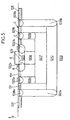
- FIG. 5 represents a bipolar pnp transistor having a vertical configuration.
- the direction D facing towards the top of the figure, is substantially perpendicular to a surface S of a substrate 1000.
- the substrate 1000 is of type p.
- Several doped zones are superimposed in the substrate 1000 under the surface S, with respect to the direction D.
- a zone 1001 of type P + constitutes the emitter zone of the transistor
- an N-type zone 1003 constitutes the transistor channel
- an intermediate zone 1004 is of type P
- a zone 1007, also of type P and said buried zone constitutes the collector of the transistor.
- a current flowing from the emitter to the collector of the transistor crosses the zones 1001, 1003, 1004 and 1007: it circulates thus parallel to the direction D.
- a deep zone 1010 is N-doped.
- An emitter contact zone E is arranged above the zone 1001, in electrical connection with it.
- Area 1003 is contiguous with basic contact areas B referenced 1002a and 1002b.
- the contact areas 1002a and 1002b are disposed at the level of the surface S, on each side of the zone 1003. They are N + doped.
- Zone 1007 is connected to collector contact areas 1005a and 1005b by electrical connection areas 1006a and 1006b. Zones of 1005a and 1005b are arranged at the surface S and are P + doped. The electrical connection areas 1006a and 1006b are formed by wells P.
- the deep zone 1010 separates the transistor from the rest of the volume of the substrate 1000. It is connected to contact zones 1008a and 1008b arranged at the level of the surface S, by areas of electrical connection 1009a and 1009b.
- the contact areas 1008a and 1008b are N + doped and the electrical connection areas 1009a and 1009b are formed by N-wells. Zone 1010 can thus be brought to a determined electrical potential.
- Electrical insulation zones 1011 for example made of silica, separate the different contact areas at the level of the surface S.
- a transistor having such a configuration occupies a reduced portion of the surface S of the substrate 1000: it can be realized with an integration level particularly high.
- a dimension of the transistor parallel to the surface S of the substrate 1000 may be, for example, about 0.25 micrometer, measured between the outer edges of two extreme 1011 insulation zones and opposite of the transistor.
- the circuit module that includes such a transistor is then particularly compact.
- circuit modules corresponding to FIGS. 3a and 3b are also given as examples. It is understood that other circuits operating in mirrors current and known to those skilled in the art can be used to modules 80 and 90.
- a circuit in accordance with the principle of the invention can be obtained by using field effect transistors, especially made according to the MOS technology (for "Metal Oxide Semiconductor ").
- MOS technology for "Metal Oxide Semiconductor ".
- the replacement of each bipolar transistor described above by a field effect transistor can be performed according to the known matching rules between different types of transistors bipolar and different types of field effect transistors.
Landscapes
- Engineering & Computer Science (AREA)
- Power Engineering (AREA)
- Amplifiers (AREA)
Applications Claiming Priority (2)
| Application Number | Priority Date | Filing Date | Title |
|---|---|---|---|
| FR0401903 | 2004-02-25 | ||
| FR0401903A FR2866764A1 (fr) | 2004-02-25 | 2004-02-25 | Circuit d'amplification de puissance et amplificateur operationnel l'incorporant |
Publications (2)
| Publication Number | Publication Date |
|---|---|
| EP1569332A1 true EP1569332A1 (de) | 2005-08-31 |
| EP1569332B1 EP1569332B1 (de) | 2010-09-15 |
Family
ID=34746442
Family Applications (1)
| Application Number | Title | Priority Date | Filing Date |
|---|---|---|---|
| EP05290377A Expired - Lifetime EP1569332B1 (de) | 2004-02-25 | 2005-02-18 | Leistungsverstärker und Operationsverstärker, der diesen beinhaltet |
Country Status (4)
| Country | Link |
|---|---|
| US (1) | US7274252B2 (de) |
| EP (1) | EP1569332B1 (de) |
| DE (1) | DE602005023555D1 (de) |
| FR (1) | FR2866764A1 (de) |
Families Citing this family (3)
| Publication number | Priority date | Publication date | Assignee | Title |
|---|---|---|---|---|
| TWI423729B (zh) * | 2010-08-31 | 2014-01-11 | Au Optronics Corp | 整合放大器的源級驅動器 |
| US8390096B2 (en) * | 2010-11-16 | 2013-03-05 | Taiwan Semiconductor Manufacturing Company, Ltd. | Adjustable holding voltage ESD protection device |
| RU2504896C1 (ru) * | 2012-08-14 | 2014-01-20 | Федеральное государственное бюджетное образовательное учреждение высшего профессионального образования "Южно-Российский государственный университет экономики и сервиса" (ФГБОУ ВПО "ЮРГУЭС") | Входной каскад быстродействующего операционного усилителя |
Citations (5)
| Publication number | Priority date | Publication date | Assignee | Title |
|---|---|---|---|---|
| US4780689A (en) * | 1987-07-20 | 1988-10-25 | Comlinear Corporation | Amplifier input circuit |
| US4833424A (en) * | 1988-04-04 | 1989-05-23 | Elantec | Linear amplifier with transient current boost |
| US5049653A (en) * | 1989-02-02 | 1991-09-17 | Comlinear Corporation | Wideband buffer amplifier with high slew rate |
| US5179355A (en) * | 1991-11-18 | 1993-01-12 | Elantec | Slew control in current feedback amplifiers |
| US6535063B1 (en) * | 2001-12-03 | 2003-03-18 | Texas Instruments Incorporated | Drive method for a cross-connected class AB output stage with shared base current in pre-driver |
Family Cites Families (4)
| Publication number | Priority date | Publication date | Assignee | Title |
|---|---|---|---|---|
| JPS5216950A (en) * | 1975-07-30 | 1977-02-08 | Hitachi Ltd | Differential amplification circuit |
| US4959622A (en) * | 1989-08-31 | 1990-09-25 | Delco Electronics Corporation | Operational amplifier with precise bias current control |
| US5028881A (en) * | 1990-05-03 | 1991-07-02 | Motorola, Inc. | Highly linear operational transconductance amplifier with low transconductance |
| US6163216A (en) * | 1998-12-18 | 2000-12-19 | Texas Instruments Tucson Corporation | Wideband operational amplifier |
-
2004
- 2004-02-25 FR FR0401903A patent/FR2866764A1/fr not_active Withdrawn
-
2005
- 2005-02-18 EP EP05290377A patent/EP1569332B1/de not_active Expired - Lifetime
- 2005-02-18 DE DE602005023555T patent/DE602005023555D1/de not_active Expired - Lifetime
- 2005-02-25 US US11/066,604 patent/US7274252B2/en not_active Expired - Fee Related
Patent Citations (5)
| Publication number | Priority date | Publication date | Assignee | Title |
|---|---|---|---|---|
| US4780689A (en) * | 1987-07-20 | 1988-10-25 | Comlinear Corporation | Amplifier input circuit |
| US4833424A (en) * | 1988-04-04 | 1989-05-23 | Elantec | Linear amplifier with transient current boost |
| US5049653A (en) * | 1989-02-02 | 1991-09-17 | Comlinear Corporation | Wideband buffer amplifier with high slew rate |
| US5179355A (en) * | 1991-11-18 | 1993-01-12 | Elantec | Slew control in current feedback amplifiers |
| US6535063B1 (en) * | 2001-12-03 | 2003-03-18 | Texas Instruments Incorporated | Drive method for a cross-connected class AB output stage with shared base current in pre-driver |
Also Published As
| Publication number | Publication date |
|---|---|
| US7274252B2 (en) | 2007-09-25 |
| US20050218944A1 (en) | 2005-10-06 |
| DE602005023555D1 (de) | 2010-10-28 |
| FR2866764A1 (fr) | 2005-08-26 |
| EP1569332B1 (de) | 2010-09-15 |
Similar Documents
| Publication | Publication Date | Title |
|---|---|---|
| FR2606954A1 (fr) | Amplificateur de puissance operationnel cmos entierement differentiel | |
| FR2819064A1 (fr) | Regulateur de tension a stabilite amelioree | |
| FR2667744A1 (fr) | Amplificateur operationnel a entrees et sorties differentielles. | |
| EP0675422B1 (de) | Regelschaltung zur Erzeugung einer temperatur- und versorgungsspannungsunabhängigen Referenzspannung | |
| FR2585201A1 (fr) | Amplificateur operationnel tout differentiel pour circuits integres en technique mos | |
| FR2546687A1 (fr) | Circuit miroir de courant | |
| FR2590697A1 (fr) | Circuit repetiteur de tension a bas decalage. | |
| EP1647091B1 (de) | Spannungsverstärker mit niedrigem verbrauch | |
| FR2532797A1 (fr) | Amplificateur differentiel | |
| EP1916762A1 (de) | Quarzoszillator mit Amplitudenregelung und einem erweiterten Temperaturbereich | |
| EP0649079A1 (de) | Geregelter Spannungsquellengenerator der Bandgapbauart | |
| EP1569332B1 (de) | Leistungsverstärker und Operationsverstärker, der diesen beinhaltet | |
| EP1362417B1 (de) | Verstärker mit symmetrischen ein- und ausgängen und mit variabler verstärkung | |
| CH639804A5 (fr) | Amplificateur dynamique en technologie cmos. | |
| EP0533230B1 (de) | Differenzverstärker, Oszillator und Mischer | |
| CH651160A5 (fr) | Amplificateur differentiel a transistors bipolaires realises en technologie cmos. | |
| EP1931030B1 (de) | Stromvorverstärker und damit verbundener Stromvergleicher | |
| FR3115427A1 (fr) | Amplificateur opérationnel | |
| FR2500969A1 (fr) | Amplificateur lineaire et circuit amplificateur a commande de gain comportant au moins un tel amplificateur | |
| EP1352302A1 (de) | Spannungsregler mit reduzierter statischen verstärkung in offenem regelkreis | |
| FR2872648A1 (fr) | Amplificateur a transconductance rapide | |
| FR2822308A1 (fr) | Circuit pour la separation de poles reposant sur l'effet miller | |
| FR2710798A1 (fr) | Chaîne d'amplification en mode de courant, amplificateur opérationnel, cellule de gain et élément d'amplification correspondants. | |
| FR2619972A1 (fr) | Etage amplificateur differentiel et configurations de circuits utilisant un tel etage | |
| FR3115426A1 (fr) | Amplificateur opérationnel |
Legal Events
| Date | Code | Title | Description |
|---|---|---|---|
| PUAI | Public reference made under article 153(3) epc to a published international application that has entered the european phase |
Free format text: ORIGINAL CODE: 0009012 |
|
| AK | Designated contracting states |
Kind code of ref document: A1 Designated state(s): AT BE BG CH CY CZ DE DK EE ES FI FR GB GR HU IE IS IT LI LT LU MC NL PL PT RO SE SI SK TR |
|
| AX | Request for extension of the european patent |
Extension state: AL BA HR LV MK YU |
|
| 17P | Request for examination filed |
Effective date: 20060210 |
|
| AKX | Designation fees paid |
Designated state(s): DE FR GB IT |
|
| GRAP | Despatch of communication of intention to grant a patent |
Free format text: ORIGINAL CODE: EPIDOSNIGR1 |
|
| GRAS | Grant fee paid |
Free format text: ORIGINAL CODE: EPIDOSNIGR3 |
|
| GRAA | (expected) grant |
Free format text: ORIGINAL CODE: 0009210 |
|
| AK | Designated contracting states |
Kind code of ref document: B1 Designated state(s): DE FR GB IT |
|
| REG | Reference to a national code |
Ref country code: GB Ref legal event code: FG4D Free format text: NOT ENGLISH |
|
| REF | Corresponds to: |
Ref document number: 602005023555 Country of ref document: DE Date of ref document: 20101028 Kind code of ref document: P |
|
| PG25 | Lapsed in a contracting state [announced via postgrant information from national office to epo] |
Ref country code: IT Free format text: LAPSE BECAUSE OF FAILURE TO SUBMIT A TRANSLATION OF THE DESCRIPTION OR TO PAY THE FEE WITHIN THE PRESCRIBED TIME-LIMIT Effective date: 20100915 |
|
| PGFP | Annual fee paid to national office [announced via postgrant information from national office to epo] |
Ref country code: DE Payment date: 20110207 Year of fee payment: 7 |
|
| PLBE | No opposition filed within time limit |
Free format text: ORIGINAL CODE: 0009261 |
|
| STAA | Information on the status of an ep patent application or granted ep patent |
Free format text: STATUS: NO OPPOSITION FILED WITHIN TIME LIMIT |
|
| PGFP | Annual fee paid to national office [announced via postgrant information from national office to epo] |
Ref country code: GB Payment date: 20110128 Year of fee payment: 7 |
|
| 26N | No opposition filed |
Effective date: 20110616 |
|
| REG | Reference to a national code |
Ref country code: DE Ref legal event code: R097 Ref document number: 602005023555 Country of ref document: DE Effective date: 20110616 |
|
| REG | Reference to a national code |
Ref country code: FR Ref legal event code: ST Effective date: 20111102 |
|
| PG25 | Lapsed in a contracting state [announced via postgrant information from national office to epo] |
Ref country code: FR Free format text: LAPSE BECAUSE OF NON-PAYMENT OF DUE FEES Effective date: 20110228 |
|
| GBPC | Gb: european patent ceased through non-payment of renewal fee |
Effective date: 20120218 |
|
| REG | Reference to a national code |
Ref country code: DE Ref legal event code: R119 Ref document number: 602005023555 Country of ref document: DE Effective date: 20120901 |
|
| PG25 | Lapsed in a contracting state [announced via postgrant information from national office to epo] |
Ref country code: GB Free format text: LAPSE BECAUSE OF NON-PAYMENT OF DUE FEES Effective date: 20120218 |
|
| PG25 | Lapsed in a contracting state [announced via postgrant information from national office to epo] |
Ref country code: DE Free format text: LAPSE BECAUSE OF NON-PAYMENT OF DUE FEES Effective date: 20120901 |