EP1569332A1 - Power amplifier and operational amplifier including the same - Google Patents
Power amplifier and operational amplifier including the same Download PDFInfo
- Publication number
- EP1569332A1 EP1569332A1 EP05290377A EP05290377A EP1569332A1 EP 1569332 A1 EP1569332 A1 EP 1569332A1 EP 05290377 A EP05290377 A EP 05290377A EP 05290377 A EP05290377 A EP 05290377A EP 1569332 A1 EP1569332 A1 EP 1569332A1
- Authority
- EP
- European Patent Office
- Prior art keywords
- transistors
- transistor
- circuit
- electrodes
- main
- Prior art date
- Legal status (The legal status is an assumption and is not a legal conclusion. Google has not performed a legal analysis and makes no representation as to the accuracy of the status listed.)
- Granted
Links
Images
Classifications
-
- H—ELECTRICITY
- H03—ELECTRONIC CIRCUITRY
- H03F—AMPLIFIERS
- H03F3/00—Amplifiers with only discharge tubes or only semiconductor devices as amplifying elements
- H03F3/30—Single-ended push-pull [SEPP] amplifiers; Phase-splitters therefor
- H03F3/3069—Single-ended push-pull [SEPP] amplifiers; Phase-splitters therefor the emitters of complementary power transistors being connected to the output
-
- H—ELECTRICITY
- H03—ELECTRONIC CIRCUITRY
- H03F—AMPLIFIERS
- H03F3/00—Amplifiers with only discharge tubes or only semiconductor devices as amplifying elements
- H03F3/30—Single-ended push-pull [SEPP] amplifiers; Phase-splitters therefor
Definitions
- the present invention relates to a power amplification circuit and an operational amplifier incorporating such a circuit.
- the circuit of power amplification is used in the operational amplifier as power output stage ("output buffer").
- High input impedance, low output impedance and significant dynamics of output current and output voltage are some of the characteristics sought for an amplification circuit of power.
- FIG. 1 is a diagram of a differential operational amplifier, known in the prior art.
- An operational amplifier comprises two cascaded amplification stages.
- An input stage designated GM, consists of a differential transconductance amplifier 10, receiving on two positive and negative inputs respective currents Ip and In, corresponding to input electric potentials Vp and Vn.
- the transconductance amplifier 10 is connected between two voltage supply terminals, respectively a positive supply terminal 5 and a negative supply terminal 6, referenced with respect to an electric ground terminal M.
- V cc + and V cc - supply terminals 5 and 6 may be, for example, +2.5 volts and -2.5 volts.
- the currents Ip and In are of the order of a few microamperes, in absolute values.
- the electrical input potentials Vp and Vn can vary between V cc - and V cc + ; they constitute the input signals of the operational amplifier.
- the output of the transconductance amplifier 10 constitutes the output from the entrance floor. It is connected to a node A which constitutes an entry of the power output stage 100. Capacitors 102 and 103 connect the node A to the power terminals 5 and 6, respectively. They stabilize the operation of the operational amplifier.
- a node D constitutes an output of the power output stage 100, and is also an output of the operational amplifier.
- a load impedance 101 (or "load” in English), of value Z L , is connected between the node D and the ground terminal M.
- the load impedance 101 is equivalent to a resistor connected in parallel with a capacitor (not shown).
- Z L can be equal, for example, to 100 ohms in module.
- the power amplification circuit which constitutes the output stage of power 100 is hereinafter referred to as circuit 100. It comprises two circuit modules 60 and 70.
- the module 60 comprises two bipolar transistors 61 and 62 of pnp type, preferably identical to each other. Issuers transistors 61 and 62 are connected to the supply terminal 5 by resistors identical, respectively, 63 and 64, of common value R. R may be equal, for example, at 1 kilo-ohm.
- the bases of transistors 61 and 62 are connected between them, and in addition to the collector of transistor 61. In other words, the transistor 61 is diode connected.
- the module 60 thus constituted forms a Widlar current source with outgoing currents, well known. He has a operation in current mirror: the currents coming out of the collectors transistors 61 and 62 are equal to each other.
- the module 70 is also a current source Widlar, but current Incoming. It has a dual structure of that of the module 60.
- the module 70 thus comprises two bipolar transistors 71 and 72 of npn type, preferably identical to each other. Each of these transistors has a transmitter connected to the supply terminal 6 by a resistor respectively 73 and 74.
- the resistors 73 and 74 have the same common value, which can also be the R value, but not necessarily.
- the respective bases of the transistors 71 and 72 are connected together, and further to the collector of transistor 71.
- a current source 7 is connected between the collectors of the transistors 61 and 71.
- the positive terminal of the source 7 is connected to the collector of transistor 71, and the negative terminal of source 7 is connected at the collector of the transistor 61.
- the current I d current delivered by the source 7 can be, for example, 200 micro-amperes.
- the circuit 100 further comprises a module 20, of the "push-pull" type.
- the module 20 comprises two intermediate bipolar transistors 1 and 2, respectively pnp and npn.
- Transistors 1 and 2 are preferably paired, that is, they have identical structures but have different types of inverted electrical dopings with respect to each other.
- the basics of transistors 1 and 2 are connected to each other and to the node A.
- the transmitters of the transistors 1 and 2 are respectively connected to the collectors of the transistors 62 and 72, respectively by a node B and a node C.
- Transistors of 3 and 4, respectively of the npn and pnp type, preferably paired, have their bases respectively connected to the nodes B and C.
- the transmitters of the transistors 3 and 4 are connected to each other and to the node D.
- the collectors of transistors 3 and 4 are respectively connected to the power supply terminals 5 and 6.
- the collector of the transistor intermediate 1 is directly connected to the power supply terminal 6, and the collector of the intermediate transistor 2 is directly connected to the terminal power supply 5.
- V A the electrical potential of the node A
- V A is also positive and varies according to an amplification characteristic of the transconductance amplifier. 10.
- V A is equal to a saturation value which depends on V cc + .
- the transistor 1 is then in a blocked state.
- a current equal to 1 flows between the emitter and the collector of the transistor 62.
- the output current of the circuit 100 is then equal to i3-i4, where i4 is the current flowing through the transistor 4, from the emitter to the collector.
- i3 and i4 are positive.
- the value of i OUT is limited by the value of i3 given by the relation (1). This value is commonly referred to as I SOURCE . It is reached when the electric input potential Vp is greater than the electric input potential Vn, and the value of the impedance 101 is sufficiently low.
- V A When the electrical potential V A reaches a sufficiently high value, the transistor 62 is in a saturated state.
- V oh is called waste voltage, it can reach 1 volt.
- the potential V D is called the electrical output potential of the circuit 100.
- V ol A waste voltage V ol , similar to V oh , limits the value that can take the potential V D when Vp-Vn is negative. The minimum value of V D is then V cc - + V ol .
- n can be between 1 and 10.
- I CONS the total current consumed by the circuit 100. It is equal to the sum of the currents flowing respectively in the resistors 63 and 64, i2 and i3.
- I CONS (3 + n) x I. It is sought to reduce this value of the total current consumed by a power amplification circuit in the idle state.
- An object of the present invention is thus to propose a new power amplification circuit which has a reduced current consumption at the idle state, for identical SOURCE and I SINK values .
- such a circuit has waste voltages substantially equal to those of a circuit according to Figure 1.
- said third circuit module comprises fifth and sixth transistors of said second type having each a first and a second main electrode and an electrode control. Said first major electrodes of said fifth and sixth transistors are respectively connected to the second terminal voltage supply by fifth and sixth resistors substantially identical. The respective control electrodes of said fifth and sixth transistors are connected together, and the control of said fifth transistor is further connected to the second main electrode of said fifth transistor. Said second electrodes of said fifth and sixth transistors comprise respectively said first and second inputs of said third module of circuit.
- said fourth circuit module may comprise a seventh and eighth transistors of said first type, each having a first and second main electrodes and a ordered. Said first main electrodes of said seventh and eighth transistors are respectively connected to the first terminal voltage supply by seventh and eighth resistors substantially identical. The respective control electrodes of said seventh and eighth transistors are connected together, and the control of said seventh transistor is further connected to the second main electrode of said seventh transistor. Said second electrodes of said seventh and eighth transistors comprise respectively said first and second outputs of said fourth module of circuit.
- At least some of the transistors of the circuit power amplifier are bipolar transistors.
- the invention also relates to an operational amplifier comprising a power amplification circuit as described above, said circuit constituting a power output stage of said operational amplifier.
- Such an operational amplifier has a total current consumption reduced and can deliver an identical output current.
- connection between the collector of the intermediate transistor 1 and the voltage supply terminal 6, as well as the connection between the collector of the intermediate transistor 2 and the voltage supply terminal 5, are deleted. They are replaced by two circuit modules additional 80 and 90.
- the module 80 is connected to the voltage supply terminal 6 by a node 87. It is recalled that the electrical potential of the power supply terminal voltage 6 is lower than that of the voltage supply terminal 5.
- the module 80 has an input 85 connected to the collector of the transistor intermediate 1, and an input 86 connected to the emitter of the transistor 62 by a node E.
- the adopted guidelines for currents i1 and i5 are shown in FIG.
- FIG 3a is an electrical diagram of a circuit module that can be used for module 80.
- This circuit module is of type source of current Widlar to incoming currents. It includes two bipolar transistors 81 and 82 npn type.
- the emitters of transistors 81 and 82 are respectively connected to the voltage supply terminal 6 by resistors 83 and 84 substantially identical.
- the respective bases of transistors 81 and 82 are interconnected, and in addition to the collector of transistor 81.
- the Transistors 81 and 82 are preferably identical to each other.
- the resistances 83 and 84 may have a value of 1 kilo-ohm, for example.
- the module 90 is connected to the voltage supply terminal 5 by a node 97.
- the module 90 has an output 95 connected to the collector of the intermediate transistor 2, and an output 96 connected to the emitter of the transistor 72 by a node F.
- the module 90 is arranged such that a current electrical i6 flowing between the output 96 and the node F is identical to a current electrical i2 entering through the collector of transistor 2.
- i6 i2: the module 90 also has a current mirror operation.
- the orientations adopted for currents i2 and i6 are shown in FIG.
- FIG. 3b is an electrical diagram of another circuit module, which can be used for module 90.
- This other circuit module is of type Widlar current source with outgoing currents.
- Bipolar transistors 91 and 92 are of the pnp type, and are preferably identical to each other. Issuers transistors 91 and 92 are respectively connected to the power supply terminal. voltage 5 by resistors 93 and 94 substantially identical.
- the basics respective transistors 91 and 92 are connected to each other, and in addition to collector of the transistor 91.
- the resistors 93 and 94 may also have a value of 1 kilo-ohm, for example.
- denotes the absolute value. Therefore, i5 is approximately equal to 1/2. It follows that the current flowing through the transistor 62 to the quiescent state (ie when Vp Vn) is also approximately equal to l / 2. The current flowing through the transistor 62 is therefore approximately equal to half the corresponding current in the case of a circuit according to FIG.
- the characteristics of a circuit 100 according to FIG. 2 are now compared with those of a circuit 100 according to FIG. 1.
- the current I of the source 7 of the circuit 100 according to FIG. 2 is adjusted. so that the two circuits have identical values of total current consumed I CONS .
- FIG. 4a illustrates the variations of I SOURCE as a function of the electrical potential of the node D when the difference Vp-Vn is positive, for each of the two circuits considered. It is therefore characteristic output curves, in voltage-current coordinates, respectively for a circuit 100 according to Figure 1 and for a circuit 100 according to Figure 2.
- Each of these characteristic curves is of the current generator type, which comprises a plateau up to a maximum value of the electrical potential of the node D, fixed by the waste voltage V oh .
- the value of I SOURCE at this plateau is about 0.038 ampere for a circuit 100 according to FIG. 1, and about 0.051 ampere for a circuit 100 according to FIG. 2.
- the increase obtained for the value of I SOURCE is therefore about 34%.
- the slope of each curve at the plateau is related to a residual variation of the electrical potentials of the electrodes of transistors 1 and 62.
- Figure 4b is similar to Figure 4a, when Vp-Vn is negative. It indicates the minimum values of the current i OUT (these minimum values being negative). It corresponds to -I SINK .
- At least one of Transistors of this module has a vertical configuration. According to such configuration, a main conduction direction of the transistor is substantially perpendicular to a surface of the substrate.
- FIG. 5 represents a bipolar pnp transistor having a vertical configuration.
- the direction D facing towards the top of the figure, is substantially perpendicular to a surface S of a substrate 1000.
- the substrate 1000 is of type p.
- Several doped zones are superimposed in the substrate 1000 under the surface S, with respect to the direction D.
- a zone 1001 of type P + constitutes the emitter zone of the transistor
- an N-type zone 1003 constitutes the transistor channel
- an intermediate zone 1004 is of type P
- a zone 1007, also of type P and said buried zone constitutes the collector of the transistor.
- a current flowing from the emitter to the collector of the transistor crosses the zones 1001, 1003, 1004 and 1007: it circulates thus parallel to the direction D.
- a deep zone 1010 is N-doped.
- An emitter contact zone E is arranged above the zone 1001, in electrical connection with it.
- Area 1003 is contiguous with basic contact areas B referenced 1002a and 1002b.
- the contact areas 1002a and 1002b are disposed at the level of the surface S, on each side of the zone 1003. They are N + doped.
- Zone 1007 is connected to collector contact areas 1005a and 1005b by electrical connection areas 1006a and 1006b. Zones of 1005a and 1005b are arranged at the surface S and are P + doped. The electrical connection areas 1006a and 1006b are formed by wells P.
- the deep zone 1010 separates the transistor from the rest of the volume of the substrate 1000. It is connected to contact zones 1008a and 1008b arranged at the level of the surface S, by areas of electrical connection 1009a and 1009b.
- the contact areas 1008a and 1008b are N + doped and the electrical connection areas 1009a and 1009b are formed by N-wells. Zone 1010 can thus be brought to a determined electrical potential.
- Electrical insulation zones 1011 for example made of silica, separate the different contact areas at the level of the surface S.
- a transistor having such a configuration occupies a reduced portion of the surface S of the substrate 1000: it can be realized with an integration level particularly high.
- a dimension of the transistor parallel to the surface S of the substrate 1000 may be, for example, about 0.25 micrometer, measured between the outer edges of two extreme 1011 insulation zones and opposite of the transistor.
- the circuit module that includes such a transistor is then particularly compact.
- circuit modules corresponding to FIGS. 3a and 3b are also given as examples. It is understood that other circuits operating in mirrors current and known to those skilled in the art can be used to modules 80 and 90.
- a circuit in accordance with the principle of the invention can be obtained by using field effect transistors, especially made according to the MOS technology (for "Metal Oxide Semiconductor ").
- MOS technology for "Metal Oxide Semiconductor ".
- the replacement of each bipolar transistor described above by a field effect transistor can be performed according to the known matching rules between different types of transistors bipolar and different types of field effect transistors.
Landscapes
- Engineering & Computer Science (AREA)
- Power Engineering (AREA)
- Amplifiers (AREA)
Abstract
Description
La présente invention concerne un circuit d'amplification de puissance et un amplificateur opérationnel incorporant un tel circuit. Le circuit d'amplification de puissance est utilisé dans l'amplificateur opérationnel comme étage de sortie de puissance («output buffer», en anglais).The present invention relates to a power amplification circuit and an operational amplifier incorporating such a circuit. The circuit of power amplification is used in the operational amplifier as power output stage ("output buffer").
Une impédance d'entrée élevée, une impédance de sortie faible et des dynamiques importantes de courant de sortie et de tension de sortie sont certaines des caractéristiques recherchées pour un circuit d'amplification de puissance.High input impedance, low output impedance and significant dynamics of output current and output voltage are some of the characteristics sought for an amplification circuit of power.
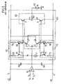
La figure 1 est un diagramme d'un amplificateur opérationnel différentiel, connu dans l'art antérieur. Un tel amplificateur opérationnel comprend deux étages d'amplification cascadés. Un étage d'entrée, désigné par GM, est constitué d'un amplificateur de transconductance différentiel 10, recevant sur deux entrées positive et négative des courants respectifs Ip et In, correspondant à des potentiels électriques d'entrée Vp et Vn. L'amplificateur de transconductance 10 est connecté entre deux bornes d'alimentation en tension, respectivement une borne d'alimentation positive 5 et une borne d'alimentation négative 6, référencées par rapport à une borne de masse électrique M. Des potentiels électriques respectifs Vcc + et Vcc - des bornes d'alimentation 5 et 6 peuvent être, par exemple, +2,5 volts et -2,5 volts. Les courants Ip et In sont de l'ordre de quelques microampères, en valeurs absolues. Les potentiels électriques d'entrée Vp et Vn peuvent varier entre Vcc - et Vcc +; ils constituent les signaux d'entrée de l'amplificateur opérationnel.Figure 1 is a diagram of a differential operational amplifier, known in the prior art. Such an operational amplifier comprises two cascaded amplification stages. An input stage, designated GM, consists of a differential transconductance amplifier 10, receiving on two positive and negative inputs respective currents Ip and In, corresponding to input electric potentials Vp and Vn. The transconductance amplifier 10 is connected between two voltage supply terminals, respectively a positive supply terminal 5 and a negative supply terminal 6, referenced with respect to an electric ground terminal M. Of the respective electrical potentials V cc + and V cc - supply terminals 5 and 6 may be, for example, +2.5 volts and -2.5 volts. The currents Ip and In are of the order of a few microamperes, in absolute values. The electrical input potentials Vp and Vn can vary between V cc - and V cc + ; they constitute the input signals of the operational amplifier.
La sortie de l'amplificateur de transconductance 10 constitue la sortie de l'étage d'entrée. Elle est reliée à un noeud A qui constitue une entrée de l'étage de sortie de puissance 100. Des condensateurs 102 et 103 relient le noeud A aux bornes d'alimentation 5 et 6, respectivement. Ils stabilisent le fonctionnement de l'amplificateur opérationnel.The output of the transconductance amplifier 10 constitutes the output from the entrance floor. It is connected to a node A which constitutes an entry of the power output stage 100. Capacitors 102 and 103 connect the node A to the power terminals 5 and 6, respectively. They stabilize the operation of the operational amplifier.
Un noeud D constitue une sortie de l'étage de sortie de puissance 100, et est aussi une sortie de l'amplificateur opérationnel. Une impédance de charge 101 (ou «load» en anglais), de valeur ZL, est connectée entre le noeud D et la borne de masse M. Usuellement, l'impédance de charge 101 est équivalente à une résistance connectée en parallèle avec un condensateur (non représentés). ZL peut être égale, par exemple, à 100 ohms en module.A node D constitutes an output of the power output stage 100, and is also an output of the operational amplifier. A load impedance 101 (or "load" in English), of value Z L , is connected between the node D and the ground terminal M. Usually, the load impedance 101 is equivalent to a resistor connected in parallel with a capacitor (not shown). Z L can be equal, for example, to 100 ohms in module.
Le circuit d'amplification de puissance qui constitue l'étage de sortie de puissance 100 est désigné dans la suite par circuit 100. Il comprend deux modules de circuit 60 et 70. Le module 60 comprend deux transistors bipolaires 61 et 62 de type pnp, de préférence identiques entre eux. Les émetteurs des transistors 61 et 62 sont reliés à la borne d'alimentation 5 par des résistances identiques respectivement 63 et 64, de valeur commune R. R peut être égale, par exemple, à 1 kilo-ohm. Les bases des transistors 61 et 62 sont connectées entre elles, et en outre au collecteur du transistor 61. Dit autrement, le transistor 61 est connecté en diode. Le module 60 ainsi constitué forme une source de courant Widlar à courants sortants, bien connue. Il possède un fonctionnement en miroir de courant : les courants sortant par les collecteurs des transistors 61 et 62 sont égaux entre eux.The power amplification circuit which constitutes the output stage of power 100 is hereinafter referred to as circuit 100. It comprises two circuit modules 60 and 70. The module 60 comprises two bipolar transistors 61 and 62 of pnp type, preferably identical to each other. Issuers transistors 61 and 62 are connected to the supply terminal 5 by resistors identical, respectively, 63 and 64, of common value R. R may be equal, for example, at 1 kilo-ohm. The bases of transistors 61 and 62 are connected between them, and in addition to the collector of transistor 61. In other words, the transistor 61 is diode connected. The module 60 thus constituted forms a Widlar current source with outgoing currents, well known. He has a operation in current mirror: the currents coming out of the collectors transistors 61 and 62 are equal to each other.
Le module 70 est aussi une source de courant Widlar, mais à courants entrants. Il présente une structure duale de celle du module 60. Le module 70 comprend ainsi deux transistors bipolaires 71 et 72 de type npn, de préférence identiques entre eux. Chacun de ces transistors possède un émetteur relié à la borne d'alimentation 6 par une résistance respectivement 73 et 74. Les résistances 73 et 74 ont une même valeur commune, qui peut être aussi la valeur R, mais non nécessairement. Les bases respectives des transistors 71 et 72 sont connectées entre elles, et en outre au collecteur du transistor 71.The module 70 is also a current source Widlar, but current Incoming. It has a dual structure of that of the module 60. The module 70 thus comprises two bipolar transistors 71 and 72 of npn type, preferably identical to each other. Each of these transistors has a transmitter connected to the supply terminal 6 by a resistor respectively 73 and 74. The resistors 73 and 74 have the same common value, which can also be the R value, but not necessarily. The respective bases of the transistors 71 and 72 are connected together, and further to the collector of transistor 71.
Une source de courant 7 est connectée entre les collecteurs des transistors 61 et 71. La borne positive de la source 7 est connectée au collecteur du transistor 71, et la borne négative de la source 7 est connectée au collecteur du transistor 61. L'intensité l d courant délivré par la source 7 peut être, par exemple, de 200 micro-ampères.A current source 7 is connected between the collectors of the transistors 61 and 71. The positive terminal of the source 7 is connected to the collector of transistor 71, and the negative terminal of source 7 is connected at the collector of the transistor 61. The current I d current delivered by the source 7 can be, for example, 200 micro-amperes.
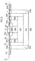
Le circuit 100 comprend en outre un module 20, de type «push-pull». Le module 20 comprend deux transistors bipolaires intermédiaires 1 et 2, respectivement pnp et npn. Les transistors 1 et 2 sont de préférence appariés, c'est-à-dire qu'ils présentent des structures identiques mais ont des types de dopages électriques inversés l'un par rapport à l'autre. Les bases des transistors 1 et 2 sont connectées entre elles et au noeud A. Les émetteurs des transistors 1 et 2 sont respectivement connectés aux collecteurs des transistors 62 et 72, respectivement par un noeud B et par un noeud C. Des transistors de sortie 3 et 4, respectivement de type npn et pnp, de préférence appariés, ont leurs bases respectivement connectées aux noeuds B et C. Les émetteurs des transistors 3 et 4 sont connectés entre eux et au noeud D. Les collecteurs des transistors 3 et 4 sont connectés respectivement aux bornes d'alimentation 5 et 6.The circuit 100 further comprises a module 20, of the "push-pull" type. The module 20 comprises two intermediate bipolar transistors 1 and 2, respectively pnp and npn. Transistors 1 and 2 are preferably paired, that is, they have identical structures but have different types of inverted electrical dopings with respect to each other. The basics of transistors 1 and 2 are connected to each other and to the node A. The transmitters of the transistors 1 and 2 are respectively connected to the collectors of the transistors 62 and 72, respectively by a node B and a node C. Transistors of 3 and 4, respectively of the npn and pnp type, preferably paired, have their bases respectively connected to the nodes B and C. The transmitters of the transistors 3 and 4 are connected to each other and to the node D. The collectors of transistors 3 and 4 are respectively connected to the power supply terminals 5 and 6.
Selon la configuration connue du circuit 100, le collecteur du transistor intermédiaire 1 est directement connecté à la borne d'alimentation 6, et le collecteur du transistor intermédiaire 2 est directement connecté à la borne d'alimentation 5.According to the known configuration of the circuit 100, the collector of the transistor intermediate 1 is directly connected to the power supply terminal 6, and the collector of the intermediate transistor 2 is directly connected to the terminal power supply 5.
Lorsque la différence Vp-Vn entre les potentiels électriques d'entrée Vp
et Vn est positive et augmente progressivement, le potentiel électrique du
noeud A, noté VA, est aussi positif et varie selon une caractéristique
d'amplification de l'amplificateur de transconductance 10. Dans la pratique, VA
est égal à une valeur de saturation qui dépend de Vcc +. Conformément au
fonctionnement connu du module 20, le transistor 1 est alors dans un état
bloqué. D'après le fonctionnement en miroir de courant du module 60, un
courant égal à l circule entre l'émetteur et le collecteur du transistor 62. Un
courant l circule par conséquent du noeud B vers la base du transistor 3. On a
alors :
Le courant de sortie du circuit 100, noté iOUT, est alors égal à i3-i4, où i4 est le courant qui traverse le transistor 4, de l'émetteur vers le collecteur. Les orientations de i3 et i4 sont indiquées sur la figure 1. i3 et i4 sont positifs. La valeur de iOUT est limitée par la valeur de i3 donnée par la relation (1). Cette valeur est couramment désignée par ISOURCE. Elle est atteinte lorsque le potentiel électrique d'entrée Vp est supérieur au potentiel électrique d'entrée Vn, et que la valeur de l'impédance 101 est suffisamment faible.The output current of the circuit 100, denoted i OUT , is then equal to i3-i4, where i4 is the current flowing through the transistor 4, from the emitter to the collector. The orientations of i3 and i4 are shown in figure 1. i3 and i4 are positive. The value of i OUT is limited by the value of i3 given by the relation (1). This value is commonly referred to as I SOURCE . It is reached when the electric input potential Vp is greater than the electric input potential Vn, and the value of the impedance 101 is sufficiently low.
Symétriquement, lorsque le potentiel électrique d'entrée Vp est
inférieur au potentiel électrique d'entrée Vn, le potentiel électrique du noeud A
est négatif. Le courant iOUT est alors négatif et limité, en valeur absolue, par la
valeur de i4 donnée par la relation (2) :
Lorsque le potentiel électrique VA atteint une valeur suffisamment
élevée, le transistor 62 est dans un état saturé. La valeur maximale que peut
atteindre le potentiel électrique VD sur le noeud D est alors Vcc +-Voh, avec :
Une tension de déchet Vol, analogue à Voh, limite la valeur que peut
prendre le potentiel VD lorsque Vp-Vn est négatif. La valeur minimale de VD est
alors Vcc -+Vol. La tension Vol a pour expression :
Par ailleurs, les émetteurs et les bases respectives des transistors 1 à
4 forment une boucle fermée. La différence entre les potentiels électriques VA
et VD est donc donnée par la relation double suivante :
A l'état de repos du circuit 100, c'est-à-dire lorsque Vp=Vn, aucun
courant ne sort du noeud D en direction de l'impédance 101 (IOUT = 0), et les
potentiels électriques des noeuds A et D sont égaux entre eux. Les courants
circulant respectivement entre le noeud B et la base du transistor 3, et entre le
noeud C et la base du transistor 4 sont très faibles par rapport au courant l. Un
courant i1 égal à l circule alors dans le transistor 1, de l'émetteur vers le
collecteur du transistor 1. De même un courant i2 égal à l circule dans le
transistor 2, du collecteur vers l'émetteur du transistor 2. Il résulte alors de la
relation (5) que i3=i4=n x I, où n est le rapport entre les surfaces respectives
des émetteurs des transistors 3 et 2, ou des transistors 4 et 1 :
A l'état de repos du circuit 100, le courant total consommé par le circuit
100, noté ICONS, est le courant qui circule entre les bornes d'alimentation 5 et
6. Il est égal à la somme des courants circulant respectivement dans les
résistances 63 et 64, de i2 et de i3. On obtient :
Un but de la présente invention consiste ainsi à proposer un nouveau circuit d'amplification de puissance qui présente une consommation de courant réduite à l'état de repos, pour des valeurs de ISOURCE et ISINK identiques.An object of the present invention is thus to propose a new power amplification circuit which has a reduced current consumption at the idle state, for identical SOURCE and I SINK values .
L'invention propose donc un circuit d'amplification de puissance qui comprend :
- une entrée et une sortie ;
- un premier module de circuit comprenant un premier et un deuxième transistors d'un même premier type et ayant chacun une première et une seconde électrodes principales et une électrode de commande, lesdites premières électrodes principales desdits premier et deuxième transistors étant respectivement reliées à une première borne d'alimentation en tension par des première et deuxième résistances sensiblement identiques, les électrodes de commande respectives desdits premier et deuxième transistors étant connectées entre elles, l'électrode de commande dudit premier transistor étant en outre connectée à la seconde électrode principale dudit premier transistor ;
- un deuxième module de circuit comprenant un troisième et un quatrième transistors d'un même second type opposé au premier type et ayant chacun une première et une seconde électrodes principales et une électrode de commande, lesdites premières électrodes principales desdits troisième et quatrième transistors étant respectivement reliées à une seconde borne d'alimentation en tension par des troisième et quatrième résistances sensiblement identiques, les électrodes de commande respectives desdits troisième et quatrième transistors étant connectées entre elles, l'électrode de commande dudit troisième transistor étant en outre connectée à la seconde électrode principale dudit troisième transistor ;
- une source de courant connectée aux dites secondes électrodes principales des premier et troisième transistors ;
- un module push-pull comprenant :
- un premier et un second transistors intermédiaires, respectivement des premier et second types et ayant chacun une première et une seconde électrodes principales et une électrode de commande, les deux électrodes de commande des premier et second transistors intermédiaires étant connectées entre elles et à l'entrée du circuit, les premières électrodes principales des premier et second transistors intermédiaires étant respectivement connectées aux secondes électrodes principales respectives desdits deuxième et quatrième transistors, respectivement par un premier et un second noeuds;
- un premier et un second transistors de sortie, respectivement des second et premier types et ayant chacun une première et une seconde électrodes principales et une électrode de commande, les électrodes de commande desdits premier et second transistors de sortie étant respectivement connectées auxdits premier et second noeuds, lesdites premières électrodes principales des premier et second transistors de sortie étant connectées entre elles et à la sortie du circuit, lesdites secondes électrodes principales des premier et second transistors de sortie étant reliées respectivement aux dites première et seconde bornes d'alimentation en tension.
- an entrance and an exit;
- a first circuit module comprising first and second transistors of the same first type and each having first and second main electrodes and a control electrode, said first main electrodes of said first and second transistors being respectively connected to a first terminal; voltage supply means by first and second substantially identical resistors, the respective control electrodes of said first and second transistors being connected to each other, the control electrode of said first transistor being further connected to the second main electrode of said first transistor;
- a second circuit module comprising third and fourth transistors of the same second type opposite the first type and each having first and second main electrodes and a control electrode, said first main electrodes of said third and fourth transistors being respectively connected; at a second voltage supply terminal by substantially identical third and fourth resistors, the respective control electrodes of said third and fourth transistors being connected to each other, the control electrode of said third transistor being further connected to the second main electrode said third transistor;
- a current source connected to said second main electrodes of the first and third transistors;
- a push-pull module comprising:
- first and second intermediate transistors, respectively first and second types and each having first and second main electrodes and a control electrode, the two control electrodes of the first and second intermediate transistors being connected to each other and to the input of the circuit, the first main electrodes of the first and second intermediate transistors being respectively connected to the second respective main electrodes of said second and fourth transistors, respectively by a first and a second node;
- first and second output transistors, respectively second and first types and each having first and second main electrodes and a control electrode, the control electrodes of said first and second output transistors being respectively connected to said first and second nodes; said first main electrodes of the first and second output transistors being connected to each other and to the output of the circuit, said second main electrodes of the first and second output transistors being respectively connected to said first and second voltage supply terminals.
Le circuit d'amplification de puissance comprend en outre :
- un troisième module de circuit ayant une première et une seconde entrées connectées respectivement à la seconde électrode principale dudit premier transistor intermédiaire et à la première électrode principale dudit deuxième transistor, et agencé de telle sorte qu'un courant électrique circulant par ladite seconde entrée est identique à un courant électrique circulant par ladite première entrée, et
- un quatrième module de circuit ayant une première et une seconde sorties connectées respectivement à la seconde électrode principale dudit second transistor intermédiaire et à la première électrode principale dudit quatrième transistor, et agencé de telle sorte qu'un courant électrique circulant par ladite seconde sortie est identique à un courant électrique circulant par ladite première sortie.
- a third circuit module having first and second inputs respectively connected to the second main electrode of said first intermediate transistor and to the first main electrode of said second transistor, and arranged such that an electric current flowing through said second input is identical an electric current flowing through said first input, and
- a fourth circuit module having first and second outputs respectively connected to the second main electrode of said second intermediate transistor and to the first main electrode of said fourth transistor, and arranged such that an electric current flowing through said second output is identical to an electric current flowing through said first output.
Ainsi, une partie du courant circulant dans la seconde résistance du premier module de circuit est envoyée dans ledit troisième module de circuit, qui fonctionne en miroir de courant. Le courant qui traverse le deuxième transistor du premier module de circuit est alors diminué, de même que le courant qui traverse ledit premier transistor intermédiaire. Cette diminution provoque une diminution du courant qui circule entre les électrodes principales du premier transistor de sortie. Il en résulte une diminution du courant total consommé par le circuit, entre les deux bornes d'alimentation en tension.Thus, a part of the current flowing in the second resistance of the first circuit module is sent into said third circuit module, which works in current mirror. The current flowing through the second transistor of the first circuit module is then decreased, as is the current flowing through said first intermediate transistor. This decrease causes a decrease in the current flowing between the main electrodes of the first output transistor. This results in a decrease in the total current consumed by the circuit, between the two power supply terminals.
Symétriquement, une partie du courant circulant dans ladite quatrième résistance du deuxième module de circuit provient dudit quatrième module de circuit fonctionnant en miroir de courant. Il en résulte des diminutions des courants circulant entre les électrodes principales dudit quatrième transistor et dudit second transistor intermédiaire, et par conséquent aussi une diminution du courant circulant entre les électrodes principales du second transistor de sortie.Symmetrically, a part of the current flowing in said fourth resistance of the second circuit module comes from said fourth module of circuit operating in current mirror. This results in decreases in currents flowing between the main electrodes of said fourth transistor and of said second intermediate transistor, and therefore also a decrease current flowing between the main electrodes of the second transistor of exit.
Par ailleurs, la valeur absolue maximale du courant de sortie d'un tel circuit est identique à celle d'un circuit conforme à la figure 1.Moreover, the maximum absolute value of the output current of such circuit is identical to that of a circuit according to Figure 1.
En outre, un tel circuit présente des tensions de déchet sensiblement égales à celles d'un circuit conforme à la figure 1.In addition, such a circuit has waste voltages substantially equal to those of a circuit according to Figure 1.
Les dynamiques du courant de sortie et du potentiel électrique de sortie du circuit ne sont donc pas réduites.The dynamics of the output current and the electrical potential of output of the circuit are not reduced.
Enfin, ce circuit est particulièrement simple et robuste. Il est donc peu onéreux et sa durée de fonctionnement est importante.Finally, this circuit is particularly simple and robust. It is therefore little expensive and its operating time is important.
Dans le mode de réalisation préféré, ledit troisième module de circuit comprend un cinquième et un sixième transistors dudit second type, ayant chacun une première et une seconde électrodes principales et une électrode de commande. Lesdites premières électrodes principales desdits cinquième et sixième transistors sont respectivement reliées à la seconde borne d'alimentation en tension par des cinquième et sixième résistances sensiblement identiques. Les électrodes de commande respectives desdits cinquième et sixième transistors sont connectées entre elles, et l'électrode de commande dudit cinquième transistor est en outre connectée à la seconde électrode principale dudit cinquième transistor. Lesdites secondes électrodes principales desdits cinquième et sixième transistors comprennent respectivement lesdites première et seconde entrées dudit troisième module de circuit.In the preferred embodiment, said third circuit module comprises fifth and sixth transistors of said second type having each a first and a second main electrode and an electrode control. Said first major electrodes of said fifth and sixth transistors are respectively connected to the second terminal voltage supply by fifth and sixth resistors substantially identical. The respective control electrodes of said fifth and sixth transistors are connected together, and the control of said fifth transistor is further connected to the second main electrode of said fifth transistor. Said second electrodes of said fifth and sixth transistors comprise respectively said first and second inputs of said third module of circuit.
De même, ledit quatrième module de circuit peut comprendre un septième et un huitième transistors dudit premier type, ayant chacun une première et une seconde électrodes principales et une électrode de commande. Lesdites premières électrodes principales desdits septième et huitième transistors sont respectivement reliées à la première borne d'alimentation en tension par des septième et huitième résistances sensiblement identiques. Les électrodes de commande respectives desdits septième et huitième transistors sont connectées entre elles, et l'électrode de commande dudit septième transistor est en outre connectée à la seconde électrode principale dudit septième transistor. Lesdites secondes électrodes principales desdits septième et huitième transistors comprennent respectivement lesdites première et seconde sorties dudit quatrième module de circuit.Likewise, said fourth circuit module may comprise a seventh and eighth transistors of said first type, each having a first and second main electrodes and a ordered. Said first main electrodes of said seventh and eighth transistors are respectively connected to the first terminal voltage supply by seventh and eighth resistors substantially identical. The respective control electrodes of said seventh and eighth transistors are connected together, and the control of said seventh transistor is further connected to the second main electrode of said seventh transistor. Said second electrodes of said seventh and eighth transistors comprise respectively said first and second outputs of said fourth module of circuit.
Avantageusement, certains au moins des transistors du circuit amplificateur de puissance sont des transistors bipolaires.Advantageously, at least some of the transistors of the circuit power amplifier are bipolar transistors.
L'invention concerne aussi un amplificateur opérationnel comprenant un circuit d'amplification de puissance tel que décrit précédemment, ledit circuit constituant un étage de sortie de puissance dudit amplificateur opérationnel. Un tel amplificateur opérationnel présente une consommation totale de courant réduite et peut délivrer un courant de sortie identique.The invention also relates to an operational amplifier comprising a power amplification circuit as described above, said circuit constituting a power output stage of said operational amplifier. Such an operational amplifier has a total current consumption reduced and can deliver an identical output current.
D'autres particularités et avantages de la présente invention apparaítront dans la description ci-après d'un exemple de réalisation non limitatif, en référence aux dessins annexés, dans lesquels :
- la figure 1, déjà décrite, est un diagramme électrique d'un amplificateur opérationnel connu ;
- la figure 2 est un diagramme électrique d'un amplificateur opérationnel comprenant un circuit d'amplification de puissance selon l'invention ;
- les figures 3a et 3b sont des diagrammes électriques de deux modules de circuit pouvant être utilisés dans un amplificateur opérationnel conforme à la figure 2 ;
- les figures 4a et 4b représentent des variations du courant de sortie maximal, en valeur absolue, pour deux circuits respectivement conformes à la figure 1 et à la figure 2 ; et
- la figure 5 illustre une configuration préférée de transistors pouvant être utilisée pour un module de circuit conforme à la figure 3b.
- Figure 1, already described, is an electrical diagram of a known operational amplifier;
- FIG. 2 is an electrical diagram of an operational amplifier comprising a power amplification circuit according to the invention;
- FIGS. 3a and 3b are electrical diagrams of two circuit modules that can be used in an operational amplifier according to FIG. 2;
- Figures 4a and 4b show variations of the maximum output current, in absolute value, for two circuits respectively according to Figure 1 and Figure 2; and
- FIG. 5 illustrates a preferred configuration of transistors that can be used for a circuit module according to FIG. 3b.
Des références identiques utilisées sur plusieurs figures correspondent à des éléments identiques, ou qui remplissent des fonctions analogues.Identical references used in several figures correspond identical elements, or which perform similar functions.
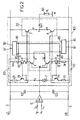
Un amplificateur opérationnel conforme à la figure 2 comprend des composants identiques à ceux d'un amplificateur opérationnel conforme à la figure 1, agencés de la même façon. La description de ces composants communs n'est pas reprise ici : on se reportera à la description de la figure 1 ci-dessus.An operational amplifier according to FIG. components identical to those of an operational amplifier conforming to the Figure 1, arranged in the same way. The description of these components common is not repeated here: we will refer to the description of Figure 1 above.
Conformément au diagramme de la figure 2, au sein du circuit 100 selon l'invention, la connexion entre le collecteur du transistor intermédiaire 1 et la borne d'alimentation en tension 6, ainsi que la connexion entre le collecteur du transistor intermédiaire 2 et la borne d'alimentation en tension 5, sont supprimées. Elles sont remplacées par deux modules de circuit supplémentaires 80 et 90.According to the diagram of Figure 2, within circuit 100 according to the invention, the connection between the collector of the intermediate transistor 1 and the voltage supply terminal 6, as well as the connection between the collector of the intermediate transistor 2 and the voltage supply terminal 5, are deleted. They are replaced by two circuit modules additional 80 and 90.
Le module 80 est connecté à la borne d'alimentation en tension 6 par un noeud 87. On rappelle que le potentiel électrique de la borne d'alimentation en tension 6 est inférieur à celui de la borne d'alimentation en tension 5. Le module 80 possède une entrée 85 connectée au collecteur du transistor intermédiaire 1, et une entrée 86 connectée à l'émetteur du transistor 62 par un noeud E. Le module 80 est agencé de telle sorte qu'un courant électrique i5 circulant entre le noeud E et l'entrée 86 est identique à un courant électrique i1 sortant du collecteur du transistor 1. Autrement dit, i5 = i1 : le module 80 possède un fonctionnement en miroir de courant. Les orientations adoptées pour les courants i1 et i5 sont indiquées sur la figure 2.The module 80 is connected to the voltage supply terminal 6 by a node 87. It is recalled that the electrical potential of the power supply terminal voltage 6 is lower than that of the voltage supply terminal 5. The module 80 has an input 85 connected to the collector of the transistor intermediate 1, and an input 86 connected to the emitter of the transistor 62 by a node E. The module 80 is arranged such that an electric current i5 flowing between the node E and the input 86 is identical to an electric current i1 leaving the collector of the transistor 1. In other words, i5 = i1: the module 80 has a mirrored current operation. The adopted guidelines for currents i1 and i5 are shown in FIG.
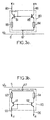
La figure 3a est un diagramme électrique d'un module de circuit qui peut être utilisé pour le module 80. Ce module de circuit est de type source de courant Widlar à courants entrants. Il comprend deux transistors bipolaires 81 et 82 de type npn. Les émetteurs des transistors 81 et 82 sont respectivement reliés à la borne d'alimentation en tension 6 par des résistances 83 et 84 sensiblement identiques. Les bases respectives des transistors 81 et 82 sont connectées entre elles, et en outre au collecteur du transistor 81. Les transistors 81 et 82 sont de préférence identiques entre eux. Les résistances 83 et 84 peuvent avoir une valeur de 1 kilo-ohm, par exemple.Figure 3a is an electrical diagram of a circuit module that can be used for module 80. This circuit module is of type source of current Widlar to incoming currents. It includes two bipolar transistors 81 and 82 npn type. The emitters of transistors 81 and 82 are respectively connected to the voltage supply terminal 6 by resistors 83 and 84 substantially identical. The respective bases of transistors 81 and 82 are interconnected, and in addition to the collector of transistor 81. The Transistors 81 and 82 are preferably identical to each other. The resistances 83 and 84 may have a value of 1 kilo-ohm, for example.
Le module 90 est connecté à la borne d'alimentation en tension 5 par un noeud 97. Le module 90 possède une sortie 95 connectée au collecteur du transistor intermédiaire 2, et une sortie 96 connectée à l'émetteur du transistor 72 par un noeud F. Le module 90 est agencé de telle sorte qu'un courant électrique i6 circulant entre la sortie 96 et le noeud F est identique à un courant électrique i2 entrant par le collecteur du transistor 2. Autrement dit, i6 = i2 : le module 90 possède aussi un fonctionnement en miroir de courant. Les orientations adoptées pour les courants i2 et i6 sont indiquées sur la figure 2.The module 90 is connected to the voltage supply terminal 5 by a node 97. The module 90 has an output 95 connected to the collector of the intermediate transistor 2, and an output 96 connected to the emitter of the transistor 72 by a node F. The module 90 is arranged such that a current electrical i6 flowing between the output 96 and the node F is identical to a current electrical i2 entering through the collector of transistor 2. In other words, i6 = i2: the module 90 also has a current mirror operation. The The orientations adopted for currents i2 and i6 are shown in FIG.
La figure 3b est un diagramme électrique d'un autre module de circuit, qui peut être utilisé pour le module 90. Cet autre module de circuit est de type source de courant Widlar à courants sortants. Les transistors bipolaires 91 et 92 sont de type pnp, et sont de préférence identiques entre eux. Les émetteurs des transistors 91 et 92 sont respectivement reliés à la borne d'alimentation en tension 5 par des résistances 93 et 94 sensiblement identiques. Les bases respectives des transistors 91 et 92 sont connectées entre elles, et en outre au collecteur du transistor 91. Les résistances 93 et 94 peuvent aussi avoir une valeur de 1 kilo-ohm, par exemple.FIG. 3b is an electrical diagram of another circuit module, which can be used for module 90. This other circuit module is of type Widlar current source with outgoing currents. Bipolar transistors 91 and 92 are of the pnp type, and are preferably identical to each other. Issuers transistors 91 and 92 are respectively connected to the power supply terminal. voltage 5 by resistors 93 and 94 substantially identical. The basics respective transistors 91 and 92 are connected to each other, and in addition to collector of the transistor 91. The resistors 93 and 94 may also have a value of 1 kilo-ohm, for example.
L'ajout des noeuds E et F respectivement dans les modules 60 et 70 a
pour conséquence que ces modules ne fonctionnent plus en miroirs de
courant. A l'état de repos du circuit 100, le courant qui circule entre le noeud B
et la base du transistor 3 est négligeable par rapport au courant entrant dans
l'émetteur du transistor 1. Le courant qui circule dans la résistance 64 est alors
2 x i5. La relation des tensions électriques dans la boucle formée par la
résistance 63, les transistors 61 et 62, et la résistance 64 est par conséquent :
Un raisonnement analogue à celui qui vient d'être présenté, appliqué au module 70 et au transistor 2, aboutit à i2 = i6 ≈ l/2 .A reasoning similar to that which has just been presented, applied to module 70 and transistor 2, leads to i2 = i6 ≈ 1/2.
Le courant total ICONS consommé dans un circuit 100 conforme à la figure 2, à l'état de repos (i.e. lorsque Vp = Vn), entre les bornes d'alimentation en tension 5 et 6, est la somme :
- du courant circulant dans la résistance 63, c'est-à-dire 1,
- du courant circulant dans la résistance 64,
- du courant entrant dans le module 90 à partir du noeud 97, et
- du courant circulant entre le collecteur et l'émetteur du transistor 3.
- current flowing in the resistor 63, i.e. 1,
- current flowing in the resistor 64,
- current entering module 90 from node 97, and
- current flowing between the collector and the emitter of transistor 3.
Le tableau 1 ci-dessous indique les valeurs de ICONS pour différentes
valeurs de n, pour deux circuits respectivement conformes à la figure 1 et à la
figure 2. Le tableau 1 indique aussi le gain relatif de consommation totale en
courant, pour un circuit conforme à la figure 2 par rapport à un circuit conforme
à la figure 1 :
Les expressions de ISOURCE et de ISINK données par les relations (1) et (2) sont encore valables pour un circuit 100 conforme à la figure 2. La valeur absolue maximale du courant iOUT est donc la même pour deux circuits 100 respectivement conformes aux figures 1 et 2.The expressions of I SOURCE and I SINK given by the relations (1) and (2) are still valid for a circuit 100 according to FIG. 2. The maximum absolute value of the current i OUT is therefore the same for two circuits 100 respectively according to Figures 1 and 2.
De même les relations (3) et (4) donnant les expressions des tensions de déchet Voh et Vol sont encore valables pour un circuit 100 conforme à la figure 2.Similarly, the relations (3) and (4) giving the expressions of the waste voltages V oh and V ol are still valid for a circuit 100 according to FIG.
On compare maintenant les caractéristiques d'un circuit 100 conforme à la figure 2 à celles d'un circuit 100 conforme à la figure 1. Pour effectuer cette comparaison, le courant I de la source 7 du circuit 100 conforme à la figure 2 est ajusté de sorte que les deux circuits présentent des valeurs identiques de courant total consommé ICONS. Pour cela, le courant I pour le circuit 100 conforme à la figure 2 est augmenté de façon à compenser le gain indiqué dans la dernière colonne du tableau 1, par exemple pour n=10. Tous les composants présents dans chacun des deux circuits considérés, qui correspondent à des mêmes références sur les figures 1 et 2, ont des valeurs identiques en dehors de la valeur l pour la source de courant 7.The characteristics of a circuit 100 according to FIG. 2 are now compared with those of a circuit 100 according to FIG. 1. In order to make this comparison, the current I of the source 7 of the circuit 100 according to FIG. 2 is adjusted. so that the two circuits have identical values of total current consumed I CONS . For this, the current I for the circuit 100 according to FIG. 2 is increased so as to compensate for the gain indicated in the last column of Table 1, for example for n = 10. All the components present in each of the two circuits considered, which correspond to the same references in FIGS. 1 and 2, have identical values outside the value 1 for the current source 7.
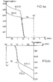
La figure 4a illustre les variations de ISOURCE en fonction du potentiel électrique du noeud D lorsque la différence Vp-Vn est positive, pour chacun des deux circuits considérés. Il s'agit donc de courbes caractéristiques de sortie, en coordonnées tension-courant, respectivement pour un circuit 100 conforme à la figure 1 et pour un circuit 100 conforme à la figure 2. Chacune de ces courbes caractéristiques est du type générateur de courant, qui comprend un plateau jusqu'à une valeur maximale du potentiel électrique du noeud D, fixée par la tension de déchet Voh. La valeur de ISOURCE au niveau de ce plateau est environ 0,038 ampère pour un circuit 100 conforme à la figure 1, et environ 0,051 ampère pour un circuit 100 conforme à la figure 2. L'augmentation obtenue pour la valeur de ISOURCE est donc de 34% environ. La pente de chaque courbe au niveau du plateau est liée à une variation résiduelle des potentiels électriques des électrodes des transistors 1 et 62.FIG. 4a illustrates the variations of I SOURCE as a function of the electrical potential of the node D when the difference Vp-Vn is positive, for each of the two circuits considered. It is therefore characteristic output curves, in voltage-current coordinates, respectively for a circuit 100 according to Figure 1 and for a circuit 100 according to Figure 2. Each of these characteristic curves is of the current generator type, which comprises a plateau up to a maximum value of the electrical potential of the node D, fixed by the waste voltage V oh . The value of I SOURCE at this plateau is about 0.038 ampere for a circuit 100 according to FIG. 1, and about 0.051 ampere for a circuit 100 according to FIG. 2. The increase obtained for the value of I SOURCE is therefore about 34%. The slope of each curve at the plateau is related to a residual variation of the electrical potentials of the electrodes of transistors 1 and 62.
Ces courbes montrent en outre que la tension de déchet Voh possède sensiblement la même valeur pour les deux circuits conformes respectivement à la figure 1 et à la figure 2. En effet, les plateaux correspondant à chacun des deux circuits présentent des longueurs identiques.These curves further show that the waste voltage V oh has substantially the same value for the two circuits respectively conforming to Figure 1 and Figure 2. Indeed, the trays corresponding to each of the two circuits have identical lengths.
La figure 4b est analogue à la figure 4a, lorsque Vp-Vn est négatif. Elle indique les valeurs minimales du courant iOUT (ces valeurs minimales étant négatives). Elle correspond donc à -ISINK.Figure 4b is similar to Figure 4a, when Vp-Vn is negative. It indicates the minimum values of the current i OUT (these minimum values being negative). It corresponds to -I SINK .
De préférence, lorsque l'un des modules de circuit 80 ou 90 est réalisé sous forme d'un circuit intégré à la surface d'un substrat S, l'un au moins des transistors de ce module a une configuration verticale. Selon une telle configuration, une direction principale de conduction du transistor est sensiblement perpendiculaire à une surface du substrat.Preferably, when one of the circuit modules 80 or 90 is realized in the form of an integrated circuit on the surface of a substrate S, at least one of Transistors of this module has a vertical configuration. According to such configuration, a main conduction direction of the transistor is substantially perpendicular to a surface of the substrate.
La figure 5 représente un transistor bipolaire de type pnp ayant une configuration verticale. La direction D, orientée vers le haut de la figure, est sensiblement perpendiculaire à une surface S d'un substrat 1000. Le substrat 1000 est de type p. Plusieurs zones dopées sont superposées dans le substrat 1000 sous la surface S, par rapport à la direction D. Une zone 1001 de type P+ constitue la zone d'émetteur du transistor, une zone 1003 de type N constitue le canal du transistor, une zone intermédiaire 1004 est de type P, et une zone 1007, aussi de type P et dite zone enterrée, constitue le collecteur du transistor. Un courant circulant de l'émetteur vers le collecteur du transistor traverse les zones 1001, 1003, 1004 et 1007 : il circule donc parallèlement à la direction D. Enfin, une zone profonde 1010 est dopée N.FIG. 5 represents a bipolar pnp transistor having a vertical configuration. The direction D, facing towards the top of the figure, is substantially perpendicular to a surface S of a substrate 1000. The substrate 1000 is of type p. Several doped zones are superimposed in the substrate 1000 under the surface S, with respect to the direction D. A zone 1001 of type P + constitutes the emitter zone of the transistor, an N-type zone 1003 constitutes the transistor channel, an intermediate zone 1004 is of type P, and a zone 1007, also of type P and said buried zone, constitutes the collector of the transistor. A current flowing from the emitter to the collector of the transistor crosses the zones 1001, 1003, 1004 and 1007: it circulates thus parallel to the direction D. Finally, a deep zone 1010 is N-doped.
Une zone de contact d'émetteur E est disposée au dessus de la zone 1001, en liaison électrique avec celle-ci.An emitter contact zone E is arranged above the zone 1001, in electrical connection with it.
La zone 1003 est contiguë avec des zones de contact de base B référencées 1002a et 1002b. Les zones de contact 1002a et 1002b sont disposées au niveau de la surface S, de chaque côté de la zone 1003. Elles sont dopées N+.Area 1003 is contiguous with basic contact areas B referenced 1002a and 1002b. The contact areas 1002a and 1002b are disposed at the level of the surface S, on each side of the zone 1003. They are N + doped.
La zone 1007 est reliée à des zones contact de collecteur 1005a et 1005b par des zones de connexion électrique 1006a et 1006b. Les zones de contact 1005a et 1005b sont disposées au niveau de la surface S et sont dopées P+. Les zones de connexion électrique 1006a et 1006b sont formées par des puits P.Zone 1007 is connected to collector contact areas 1005a and 1005b by electrical connection areas 1006a and 1006b. Zones of 1005a and 1005b are arranged at the surface S and are P + doped. The electrical connection areas 1006a and 1006b are formed by wells P.
Enfin, la zone profonde 1010 sépare le transistor du reste du volume du substrat 1000. Elle est reliée à des zones de contact 1008a et 1008b disposées au niveau de la surface S, par des zones de connexion électrique 1009a et 1009b. Les zones de contact 1008a et 1008b sont dopées N+ et les zones de connexion électrique 1009a et 1009b sont formées par des puits N. La zone 1010 peut ainsi être portée à un potentiel électrique déterminé.Finally, the deep zone 1010 separates the transistor from the rest of the volume of the substrate 1000. It is connected to contact zones 1008a and 1008b arranged at the level of the surface S, by areas of electrical connection 1009a and 1009b. The contact areas 1008a and 1008b are N + doped and the electrical connection areas 1009a and 1009b are formed by N-wells. Zone 1010 can thus be brought to a determined electrical potential.
Des zones d'isolation électrique 1011, par exemple en silice, séparent les différentes zones de contact au niveau de la surface S.Electrical insulation zones 1011, for example made of silica, separate the different contact areas at the level of the surface S.
Un transistor ayant une telle configuration occupe une partie réduite de la surface S du substrat 1000 : il peut être réalisé avec un niveau d'intégration particulièrement élevé. Une dimension du transistor parallèlement à la surface S du substrat 1000 peut être, par exemple, 0,25 micromètre environ, mesurée entre les bords extérieurs de deux zones d'isolation 1011 extrêmes et opposées du transistor. Le module de circuit qui comprend un tel transistor est alors particulièrement compact.A transistor having such a configuration occupies a reduced portion of the surface S of the substrate 1000: it can be realized with an integration level particularly high. A dimension of the transistor parallel to the surface S of the substrate 1000 may be, for example, about 0.25 micrometer, measured between the outer edges of two extreme 1011 insulation zones and opposite of the transistor. The circuit module that includes such a transistor is then particularly compact.
La configuration d'un transistor illustrée par la figure 5 est donnée à titre d'exemple. D'autres configurations équivalentes peuvent être utilisées, qui procurent des possibilités d'intégration équivalentes.The configuration of a transistor illustrated in FIG. as an example. Other equivalent configurations can be used, which provide equivalent integration opportunities.
Les modules de circuit correspondant aux figures 3a et 3b sont aussi donnés à titre d'exemples. Il est entendu que d'autres circuits fonctionnant en miroirs de courant et connus de l'Homme du métier peuvent être utilisés pour les modules 80 et 90.The circuit modules corresponding to FIGS. 3a and 3b are also given as examples. It is understood that other circuits operating in mirrors current and known to those skilled in the art can be used to modules 80 and 90.
Enfin, il est aussi entendu qu'un circuit conforme au principe de l'invention peut être obtenu en utilisant des transistors à effet de champ, notamment réalisés selon la technologie MOS (pour «Metal Oxide Semiconductor» en anglais). Le remplacement de chaque transistor bipolaire décrit plus haut par un transistor à effet de champ peut être effectué selon les règles de correspondance connues entre les différents types de transistors bipolaires et les différents types de transistors à effet de champ.Finally, it is also understood that a circuit in accordance with the principle of the invention can be obtained by using field effect transistors, especially made according to the MOS technology (for "Metal Oxide Semiconductor "). The replacement of each bipolar transistor described above by a field effect transistor can be performed according to the known matching rules between different types of transistors bipolar and different types of field effect transistors.
Claims (6)
Applications Claiming Priority (2)
| Application Number | Priority Date | Filing Date | Title |
|---|---|---|---|
| FR0401903A FR2866764A1 (en) | 2004-02-25 | 2004-02-25 | Power amplifying circuit for operational amplifier, has one circuit module with inputs coupled to main electrodes of one set of transistors, and another circuit module with outputs connected to main electrodes of another set of transistors |
| FR0401903 | 2004-02-25 |
Publications (2)
| Publication Number | Publication Date |
|---|---|
| EP1569332A1 true EP1569332A1 (en) | 2005-08-31 |
| EP1569332B1 EP1569332B1 (en) | 2010-09-15 |
Family
ID=34746442
Family Applications (1)
| Application Number | Title | Priority Date | Filing Date |
|---|---|---|---|
| EP05290377A Expired - Lifetime EP1569332B1 (en) | 2004-02-25 | 2005-02-18 | Power amplifier and operational amplifier including the same |
Country Status (4)
| Country | Link |
|---|---|
| US (1) | US7274252B2 (en) |
| EP (1) | EP1569332B1 (en) |
| DE (1) | DE602005023555D1 (en) |
| FR (1) | FR2866764A1 (en) |
Families Citing this family (3)
| Publication number | Priority date | Publication date | Assignee | Title |
|---|---|---|---|---|
| TWI423729B (en) * | 2010-08-31 | 2014-01-11 | Au Optronics Corp | Source driver having amplifiers integrated therein |
| US8390096B2 (en) * | 2010-11-16 | 2013-03-05 | Taiwan Semiconductor Manufacturing Company, Ltd. | Adjustable holding voltage ESD protection device |
| RU2504896C1 (en) * | 2012-08-14 | 2014-01-20 | Федеральное государственное бюджетное образовательное учреждение высшего профессионального образования "Южно-Российский государственный университет экономики и сервиса" (ФГБОУ ВПО "ЮРГУЭС") | Input stage of high-speed operational amplifier |
Citations (5)
| Publication number | Priority date | Publication date | Assignee | Title |
|---|---|---|---|---|
| US4780689A (en) * | 1987-07-20 | 1988-10-25 | Comlinear Corporation | Amplifier input circuit |
| US4833424A (en) * | 1988-04-04 | 1989-05-23 | Elantec | Linear amplifier with transient current boost |
| US5049653A (en) * | 1989-02-02 | 1991-09-17 | Comlinear Corporation | Wideband buffer amplifier with high slew rate |
| US5179355A (en) * | 1991-11-18 | 1993-01-12 | Elantec | Slew control in current feedback amplifiers |
| US6535063B1 (en) * | 2001-12-03 | 2003-03-18 | Texas Instruments Incorporated | Drive method for a cross-connected class AB output stage with shared base current in pre-driver |
Family Cites Families (4)
| Publication number | Priority date | Publication date | Assignee | Title |
|---|---|---|---|---|
| JPS5216950A (en) * | 1975-07-30 | 1977-02-08 | Hitachi Ltd | Differential amplification circuit |
| US4959622A (en) * | 1989-08-31 | 1990-09-25 | Delco Electronics Corporation | Operational amplifier with precise bias current control |
| US5028881A (en) * | 1990-05-03 | 1991-07-02 | Motorola, Inc. | Highly linear operational transconductance amplifier with low transconductance |
| US6163216A (en) * | 1998-12-18 | 2000-12-19 | Texas Instruments Tucson Corporation | Wideband operational amplifier |
-
2004
- 2004-02-25 FR FR0401903A patent/FR2866764A1/en not_active Withdrawn
-
2005
- 2005-02-18 DE DE602005023555T patent/DE602005023555D1/en not_active Expired - Lifetime
- 2005-02-18 EP EP05290377A patent/EP1569332B1/en not_active Expired - Lifetime
- 2005-02-25 US US11/066,604 patent/US7274252B2/en not_active Expired - Fee Related
Patent Citations (5)
| Publication number | Priority date | Publication date | Assignee | Title |
|---|---|---|---|---|
| US4780689A (en) * | 1987-07-20 | 1988-10-25 | Comlinear Corporation | Amplifier input circuit |
| US4833424A (en) * | 1988-04-04 | 1989-05-23 | Elantec | Linear amplifier with transient current boost |
| US5049653A (en) * | 1989-02-02 | 1991-09-17 | Comlinear Corporation | Wideband buffer amplifier with high slew rate |
| US5179355A (en) * | 1991-11-18 | 1993-01-12 | Elantec | Slew control in current feedback amplifiers |
| US6535063B1 (en) * | 2001-12-03 | 2003-03-18 | Texas Instruments Incorporated | Drive method for a cross-connected class AB output stage with shared base current in pre-driver |
Also Published As
| Publication number | Publication date |
|---|---|
| FR2866764A1 (en) | 2005-08-26 |
| EP1569332B1 (en) | 2010-09-15 |
| US7274252B2 (en) | 2007-09-25 |
| DE602005023555D1 (en) | 2010-10-28 |
| US20050218944A1 (en) | 2005-10-06 |
Similar Documents
| Publication | Publication Date | Title |
|---|---|---|
| FR2606954A1 (en) | FULLY DIFFERENTIAL CMOS OPERATIONAL POWER AMPLIFIER | |
| FR2819064A1 (en) | VOLTAGE REGULATOR WITH IMPROVED STABILITY | |
| EP0660512B1 (en) | Phase shifter amplifier and its application in a recombiner circuit | |
| EP0675422B1 (en) | Regulator circuit generating a reference voltage independent of temperature or supply voltage | |
| FR2585201A1 (en) | DIFFERENTIAL OPERATIONAL AMPLIFIER FOR INTEGRATED CIRCUITS IN MOS TECHNOLOGY | |
| FR2546687A1 (en) | CIRCUIT MIRROR OF CURRENT | |
| FR2590697A1 (en) | LOW DIFFERENTIAL VOLTAGE REPEATER CIRCUIT. | |
| EP1647091B1 (en) | Low-consumption voltage amplifier | |
| FR2532797A1 (en) | DIFFERENTIAL AMPLIFIER | |
| EP1916762A1 (en) | Quartz oscillator with amplitude control and an extended temperature range. | |
| EP0649079A1 (en) | Regulated voltage generating circuit of bandgap type | |
| EP1569332B1 (en) | Power amplifier and operational amplifier including the same | |
| EP1362417B1 (en) | Variable-gain differential input and output amplifier | |
| FR2487605A1 (en) | GAIN CONTROL CIRCUIT | |
| CH639804A5 (en) | DYNAMIC AMPLIFIER IN CMOS TECHNOLOGY. | |
| EP0533230B1 (en) | Differential amplifier and mixer oscillator incorporating the same | |
| CH651160A5 (en) | DIFFERENTIAL AMPLIFIER WITH BIPOLAR TRANSISTORS REALIZED IN CMOS TECHNOLOGY. | |
| EP1931030B1 (en) | Current preamplifier and associated current comparator | |
| FR3115427A1 (en) | Operational amplifier | |
| FR2500969A1 (en) | LINEAR AMPLIFIER AND AMPLIFIER CIRCUIT WITH GAIN CONTROL COMPRISING AT LEAST ONE SUCH AMPLIFIER | |
| EP1352302A1 (en) | Voltage regulator with static gain in reduced open loop | |
| FR2872648A1 (en) | FAST TRANSCONDUCTANCE AMPLIFIER | |
| EP0556927B1 (en) | Differential circuit with high linearity | |
| FR2822308A1 (en) | Circuit for separating poles between two stages of amplifier circuit, based on Miller effect and comprising resistive voltage divider bridge and two capacitors in serial branch | |
| FR2710798A1 (en) | Amplification chain in current mode, operational amplifier, gain cell and corresponding amplification element. |
Legal Events
| Date | Code | Title | Description |
|---|---|---|---|
| PUAI | Public reference made under article 153(3) epc to a published international application that has entered the european phase |
Free format text: ORIGINAL CODE: 0009012 |
|
| AK | Designated contracting states |
Kind code of ref document: A1 Designated state(s): AT BE BG CH CY CZ DE DK EE ES FI FR GB GR HU IE IS IT LI LT LU MC NL PL PT RO SE SI SK TR |
|
| AX | Request for extension of the european patent |
Extension state: AL BA HR LV MK YU |
|
| 17P | Request for examination filed |
Effective date: 20060210 |
|
| AKX | Designation fees paid |
Designated state(s): DE FR GB IT |
|
| GRAP | Despatch of communication of intention to grant a patent |
Free format text: ORIGINAL CODE: EPIDOSNIGR1 |
|
| GRAS | Grant fee paid |
Free format text: ORIGINAL CODE: EPIDOSNIGR3 |
|
| GRAA | (expected) grant |
Free format text: ORIGINAL CODE: 0009210 |
|
| AK | Designated contracting states |
Kind code of ref document: B1 Designated state(s): DE FR GB IT |
|
| REG | Reference to a national code |
Ref country code: GB Ref legal event code: FG4D Free format text: NOT ENGLISH |
|
| REF | Corresponds to: |
Ref document number: 602005023555 Country of ref document: DE Date of ref document: 20101028 Kind code of ref document: P |
|
| PG25 | Lapsed in a contracting state [announced via postgrant information from national office to epo] |
Ref country code: IT Free format text: LAPSE BECAUSE OF FAILURE TO SUBMIT A TRANSLATION OF THE DESCRIPTION OR TO PAY THE FEE WITHIN THE PRESCRIBED TIME-LIMIT Effective date: 20100915 |
|
| PGFP | Annual fee paid to national office [announced via postgrant information from national office to epo] |
Ref country code: DE Payment date: 20110207 Year of fee payment: 7 |
|
| PLBE | No opposition filed within time limit |
Free format text: ORIGINAL CODE: 0009261 |
|
| STAA | Information on the status of an ep patent application or granted ep patent |
Free format text: STATUS: NO OPPOSITION FILED WITHIN TIME LIMIT |
|
| PGFP | Annual fee paid to national office [announced via postgrant information from national office to epo] |
Ref country code: GB Payment date: 20110128 Year of fee payment: 7 |
|
| 26N | No opposition filed |
Effective date: 20110616 |
|
| REG | Reference to a national code |
Ref country code: DE Ref legal event code: R097 Ref document number: 602005023555 Country of ref document: DE Effective date: 20110616 |
|
| REG | Reference to a national code |
Ref country code: FR Ref legal event code: ST Effective date: 20111102 |
|
| PG25 | Lapsed in a contracting state [announced via postgrant information from national office to epo] |
Ref country code: FR Free format text: LAPSE BECAUSE OF NON-PAYMENT OF DUE FEES Effective date: 20110228 |
|
| GBPC | Gb: european patent ceased through non-payment of renewal fee |
Effective date: 20120218 |
|
| REG | Reference to a national code |
Ref country code: DE Ref legal event code: R119 Ref document number: 602005023555 Country of ref document: DE Effective date: 20120901 |
|
| PG25 | Lapsed in a contracting state [announced via postgrant information from national office to epo] |
Ref country code: GB Free format text: LAPSE BECAUSE OF NON-PAYMENT OF DUE FEES Effective date: 20120218 |
|
| PG25 | Lapsed in a contracting state [announced via postgrant information from national office to epo] |
Ref country code: DE Free format text: LAPSE BECAUSE OF NON-PAYMENT OF DUE FEES Effective date: 20120901 |