EP1569273A2 - Lignes conductrices enterrées dans des zones d'isolement - Google Patents
Lignes conductrices enterrées dans des zones d'isolement Download PDFInfo
- Publication number
- EP1569273A2 EP1569273A2 EP05104911A EP05104911A EP1569273A2 EP 1569273 A2 EP1569273 A2 EP 1569273A2 EP 05104911 A EP05104911 A EP 05104911A EP 05104911 A EP05104911 A EP 05104911A EP 1569273 A2 EP1569273 A2 EP 1569273A2
- Authority
- EP
- European Patent Office
- Prior art keywords
- active
- zone
- substrate
- isolation
- integrated circuit
- Prior art date
- Legal status (The legal status is an assumption and is not a legal conclusion. Google has not performed a legal analysis and makes no representation as to the accuracy of the status listed.)
- Withdrawn
Links
Images




Classifications
-
- H—ELECTRICITY
- H10—SEMICONDUCTOR DEVICES; ELECTRIC SOLID-STATE DEVICES NOT OTHERWISE PROVIDED FOR
- H10W—GENERIC PACKAGES, INTERCONNECTIONS, CONNECTORS OR OTHER CONSTRUCTIONAL DETAILS OF DEVICES COVERED BY CLASS H10
- H10W20/00—Interconnections in chips, wafers or substrates
- H10W20/01—Manufacture or treatment
- H10W20/021—Manufacture or treatment of interconnections within wafers or substrates
-
- H—ELECTRICITY
- H10—SEMICONDUCTOR DEVICES; ELECTRIC SOLID-STATE DEVICES NOT OTHERWISE PROVIDED FOR
- H10B—ELECTRONIC MEMORY DEVICES
- H10B10/00—Static random access memory [SRAM] devices
-
- H—ELECTRICITY
- H10—SEMICONDUCTOR DEVICES; ELECTRIC SOLID-STATE DEVICES NOT OTHERWISE PROVIDED FOR
- H10B—ELECTRONIC MEMORY DEVICES
- H10B10/00—Static random access memory [SRAM] devices
- H10B10/12—Static random access memory [SRAM] devices comprising a MOSFET load element
-
- H—ELECTRICITY
- H10—SEMICONDUCTOR DEVICES; ELECTRIC SOLID-STATE DEVICES NOT OTHERWISE PROVIDED FOR
- H10W—GENERIC PACKAGES, INTERCONNECTIONS, CONNECTORS OR OTHER CONSTRUCTIONAL DETAILS OF DEVICES COVERED BY CLASS H10
- H10W10/00—Isolation regions in semiconductor bodies between components of integrated devices
- H10W10/01—Manufacture or treatment
- H10W10/011—Manufacture or treatment of isolation regions comprising dielectric materials
- H10W10/014—Manufacture or treatment of isolation regions comprising dielectric materials using trench refilling with dielectric materials, e.g. shallow trench isolations
-
- H—ELECTRICITY
- H10—SEMICONDUCTOR DEVICES; ELECTRIC SOLID-STATE DEVICES NOT OTHERWISE PROVIDED FOR
- H10W—GENERIC PACKAGES, INTERCONNECTIONS, CONNECTORS OR OTHER CONSTRUCTIONAL DETAILS OF DEVICES COVERED BY CLASS H10
- H10W10/00—Isolation regions in semiconductor bodies between components of integrated devices
- H10W10/01—Manufacture or treatment
- H10W10/051—Manufacture or treatment of isolation region based on field-effect
-
- H—ELECTRICITY
- H10—SEMICONDUCTOR DEVICES; ELECTRIC SOLID-STATE DEVICES NOT OTHERWISE PROVIDED FOR
- H10W—GENERIC PACKAGES, INTERCONNECTIONS, CONNECTORS OR OTHER CONSTRUCTIONAL DETAILS OF DEVICES COVERED BY CLASS H10
- H10W10/00—Isolation regions in semiconductor bodies between components of integrated devices
- H10W10/10—Isolation regions comprising dielectric materials
- H10W10/17—Isolation regions comprising dielectric materials formed using trench refilling with dielectric materials, e.g. shallow trench isolations
-
- H—ELECTRICITY
- H10—SEMICONDUCTOR DEVICES; ELECTRIC SOLID-STATE DEVICES NOT OTHERWISE PROVIDED FOR
- H10W—GENERIC PACKAGES, INTERCONNECTIONS, CONNECTORS OR OTHER CONSTRUCTIONAL DETAILS OF DEVICES COVERED BY CLASS H10
- H10W10/00—Isolation regions in semiconductor bodies between components of integrated devices
- H10W10/50—Isolation regions based on field-effect
-
- H—ELECTRICITY
- H10—SEMICONDUCTOR DEVICES; ELECTRIC SOLID-STATE DEVICES NOT OTHERWISE PROVIDED FOR
- H10W—GENERIC PACKAGES, INTERCONNECTIONS, CONNECTORS OR OTHER CONSTRUCTIONAL DETAILS OF DEVICES COVERED BY CLASS H10
- H10W20/00—Interconnections in chips, wafers or substrates
- H10W20/01—Manufacture or treatment
- H10W20/031—Manufacture or treatment of conductive parts of the interconnections
-
- H—ELECTRICITY
- H10—SEMICONDUCTOR DEVICES; ELECTRIC SOLID-STATE DEVICES NOT OTHERWISE PROVIDED FOR
- H10W—GENERIC PACKAGES, INTERCONNECTIONS, CONNECTORS OR OTHER CONSTRUCTIONAL DETAILS OF DEVICES COVERED BY CLASS H10
- H10W20/00—Interconnections in chips, wafers or substrates
- H10W20/01—Manufacture or treatment
- H10W20/031—Manufacture or treatment of conductive parts of the interconnections
- H10W20/069—Manufacture or treatment of conductive parts of the interconnections by forming self-aligned vias or self-aligned contact plugs
-
- H—ELECTRICITY
- H10—SEMICONDUCTOR DEVICES; ELECTRIC SOLID-STATE DEVICES NOT OTHERWISE PROVIDED FOR
- H10W—GENERIC PACKAGES, INTERCONNECTIONS, CONNECTORS OR OTHER CONSTRUCTIONAL DETAILS OF DEVICES COVERED BY CLASS H10
- H10W20/00—Interconnections in chips, wafers or substrates
- H10W20/01—Manufacture or treatment
- H10W20/031—Manufacture or treatment of conductive parts of the interconnections
- H10W20/069—Manufacture or treatment of conductive parts of the interconnections by forming self-aligned vias or self-aligned contact plugs
- H10W20/0696—Manufacture or treatment of conductive parts of the interconnections by forming self-aligned vias or self-aligned contact plugs by using sacrificial placeholders, e.g. using sacrificial plugs
-
- H—ELECTRICITY
- H10—SEMICONDUCTOR DEVICES; ELECTRIC SOLID-STATE DEVICES NOT OTHERWISE PROVIDED FOR
- H10W—GENERIC PACKAGES, INTERCONNECTIONS, CONNECTORS OR OTHER CONSTRUCTIONAL DETAILS OF DEVICES COVERED BY CLASS H10
- H10W20/00—Interconnections in chips, wafers or substrates
- H10W20/01—Manufacture or treatment
- H10W20/031—Manufacture or treatment of conductive parts of the interconnections
- H10W20/0698—Local interconnections
-
- H—ELECTRICITY
- H10—SEMICONDUCTOR DEVICES; ELECTRIC SOLID-STATE DEVICES NOT OTHERWISE PROVIDED FOR
- H10W—GENERIC PACKAGES, INTERCONNECTIONS, CONNECTORS OR OTHER CONSTRUCTIONAL DETAILS OF DEVICES COVERED BY CLASS H10
- H10W20/00—Interconnections in chips, wafers or substrates
- H10W20/01—Manufacture or treatment
- H10W20/071—Manufacture or treatment of dielectric parts thereof
- H10W20/081—Manufacture or treatment of dielectric parts thereof by forming openings in the dielectric parts
-
- H—ELECTRICITY
- H10—SEMICONDUCTOR DEVICES; ELECTRIC SOLID-STATE DEVICES NOT OTHERWISE PROVIDED FOR
- H10W—GENERIC PACKAGES, INTERCONNECTIONS, CONNECTORS OR OTHER CONSTRUCTIONAL DETAILS OF DEVICES COVERED BY CLASS H10
- H10W20/00—Interconnections in chips, wafers or substrates
- H10W20/20—Interconnections within wafers or substrates, e.g. through-silicon vias [TSV]
-
- H—ELECTRICITY
- H10—SEMICONDUCTOR DEVICES; ELECTRIC SOLID-STATE DEVICES NOT OTHERWISE PROVIDED FOR
- H10D—INORGANIC ELECTRIC SEMICONDUCTOR DEVICES
- H10D30/00—Field-effect transistors [FET]
- H10D30/60—Insulated-gate field-effect transistors [IGFET]
-
- H—ELECTRICITY
- H10—SEMICONDUCTOR DEVICES; ELECTRIC SOLID-STATE DEVICES NOT OTHERWISE PROVIDED FOR
- H10W—GENERIC PACKAGES, INTERCONNECTIONS, CONNECTORS OR OTHER CONSTRUCTIONAL DETAILS OF DEVICES COVERED BY CLASS H10
- H10W20/00—Interconnections in chips, wafers or substrates
- H10W20/40—Interconnections external to wafers or substrates, e.g. back-end-of-line [BEOL] metallisations or vias connecting to gate electrodes
-
- H—ELECTRICITY
- H10—SEMICONDUCTOR DEVICES; ELECTRIC SOLID-STATE DEVICES NOT OTHERWISE PROVIDED FOR
- H10W—GENERIC PACKAGES, INTERCONNECTIONS, CONNECTORS OR OTHER CONSTRUCTIONAL DETAILS OF DEVICES COVERED BY CLASS H10
- H10W20/00—Interconnections in chips, wafers or substrates
- H10W20/40—Interconnections external to wafers or substrates, e.g. back-end-of-line [BEOL] metallisations or vias connecting to gate electrodes
- H10W20/41—Interconnections external to wafers or substrates, e.g. back-end-of-line [BEOL] metallisations or vias connecting to gate electrodes characterised by their conductive parts
- H10W20/427—Power or ground buses
Definitions
- the present invention relates to integrated circuits and more particularly the distribution networks of a reference voltage such as a supply voltage or the mass.
- An integrated circuit generally comprises a network distribution of the supply voltage Vdd, a network of distribution of the GND mass, and possibly networks of distribution of other reference voltages, for example Vdd / 2, formed above the integrated circuit.
- the conductive lines of the distribution networks are part of the conductive lines of the interconnection network of the integrated circuit. Conductive lines of the interconnection network are formed over several levels and are connected to each other by conductive vias.
- Each of these distribution networks is generally consisting of relatively long and wide parallel rails formed on one of the levels of the circuit interconnection network integrated.
- the space occupied by the lines of these networks of distribution is relatively large which has the effect of limit the space available for the other lines of the circuit generally intended to transmit signals. But the weak available space for these lines makes that they are often narrow and therefore have resistance relatively important which is detrimental in some circuits such as memories.
- the distribution of tensions of reference requires the provision of conductive lines formed on the different levels of the interconnection network. Space occupied by these conductive distribution lines can become important, which is detrimental to making connections for transmitting signals.
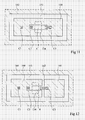
- said circuit element is a terminal of a component or polarization outlet of the substrate or a caisson formed in the substrate.
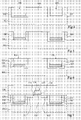
- a contact 440 is placed above the lower portion of the active zone 400 and extends to the left above an isolation area.
- a contact 441 is placed above the lower portion of the active area 402 and extends to the left over an area isolation.
- a contact 442 is placed above the portion upper active area 401 and extends to the right above an isolation zone.
- a 443 contact is placed above of the upper portion of the active zone 403 and extends on the right above an isolation area.
- the conductive regions placed in the portions 451 and 454 respectively to the left of the active zone 400 and to the right of the active zone 401 are both connected to GND mass.
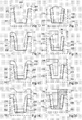
- the N-type caisson 412 is placed under the zone active 402 and under a portion of isolation areas 452 and 453.
- the casings of type P 410 and 411 are placed respectively at left and right of the N-type well 412.
- the isolation areas and the active areas are covered with an insulating layer 455.
- Contacts 440, 441 and 433 are placed in openings of the insulating layer 455.
- the contact 440 covers the area active 400, the insulating layer placed against the walls of the isolation zone 451 and the conductive region connected to GND within the isolation area 451.
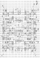
- the two rows represented are connected to the other by a relay block described below.
- Active areas 400 points P5 and P7 are connected by an active zone 530. From same, the active areas 400 of the points P6 and P8 are connected by active zone 531. Active zones 401 of points P5 and P7 are connected by an active zone 532. The active zones 401 of the points P6 and P8 are connected by an active zone 533.
- the zones 530, 531, 532 and 533 are N-type doped.
- N 412 pairs of points P5 / P7 and P6 / P8 are connected respectively by caissons N 534 and 535.
- the caissons P of points P5 / P7 and P6 / P8 are similarly connected by caissons P.
- two grid areas 542 and 543 are placed perpendicularly active zones 532 and 533.
- An active zone 545 is placed between the grid areas 542 and 543 and connects the active zones 532 and 533.
- Active zone 545 is doped with P-type unlike the active zones 532 and 533 which are doped with type N.
- a contact 546 is placed above the active zone 545 and extends above the isolation areas below and over active area 545 and extends above grid areas 542 and 543. The contact 546 is connected to the mass.
- the contact 546 makes it possible to polarize the P boxes under the active zone 545 and the GND rail placed inside the isolation areas covered by the contact 546.
- the four NMOS transistors formed by the zones of grid 442, 443 and active areas 432 and 433 are all non drivers because their grids are grounded.
- distribution networks can serve to convey any reference voltage of a circuit integrated.
Landscapes
- Semiconductor Memories (AREA)
- Element Separation (AREA)
Abstract
Description
Claims (6)
- Circuit intégré comprenant un substrat semiconducteur (101) dans lequel des zones actives (104) entourent ou sont entourées par des évidements remplis d'isolant, caractérisé en ce qu'une région conductrice (140, 141) est noyée dans l'isolant d'au moins un évidement (125, 126), la région conductrice étant connectée à une tension de référence et étant connectée à au moins un élément voisin du circuit.
- Circuit intégré selon la revendication 1, dans lequel la région conductrice est connectée à une ligne conductrice d'alimentation ou de masse (GND, Vdd) d'un réseau d'interconnexion.
- Circuit intégré selon la revendication 1, dans lequel ledit élément du circuit est une borne d'un composant (132) ou une prise de polarisation du substrat ou d'un caisson formé dans le substrat.
- Circuit intégré selon la revendication 1, comprenant des composants (130) formés dans des zones actives (104), le substrat et les composants étant recouverts d'une couche isolante de protection (138), une portion d'une zone active adjacente à un desdits au moins un évidement étant reliée à la région conductrice (141) de cet évidement par l'intermédiaire d'un contact métallique (103) placé dans une unique ouverture (03) de la couche isolante de protection et de l'isolant recouvrant la région conductrice.
- Circuit selon la revendication 1, dans lequel le substrat semiconducteur (201) est en silicium monocristallin, ledit isolant (202, 210, 211) étant constitué d'oxyde de silicium et de nitrure.
- Circuit intégré selon la revendication 1 constituant une mémoire de type SRAM, dans lequel le réseau de distribution des tensions d'alimentation et de masse est constitué d'un réseau de régions conductrices noyées dans plusieurs évidements du substrat, les régions conductrices étant reliées à plusieurs zones de source/drain des transistors MOS de la mémoire par des contacts.
Applications Claiming Priority (3)
| Application Number | Priority Date | Filing Date | Title |
|---|---|---|---|
| FR0350382 | 2003-07-30 | ||
| FR0350382 | 2003-07-30 | ||
| EP04103661A EP1503411A1 (fr) | 2003-07-30 | 2004-07-29 | Lignes conductrices enterrées dans des zones d'isolement |
Related Parent Applications (1)
| Application Number | Title | Priority Date | Filing Date |
|---|---|---|---|
| EP04103661A Division EP1503411A1 (fr) | 2003-07-30 | 2004-07-29 | Lignes conductrices enterrées dans des zones d'isolement |
Publications (2)
| Publication Number | Publication Date |
|---|---|
| EP1569273A2 true EP1569273A2 (fr) | 2005-08-31 |
| EP1569273A3 EP1569273A3 (fr) | 2005-09-14 |
Family
ID=33523105
Family Applications (2)
| Application Number | Title | Priority Date | Filing Date |
|---|---|---|---|
| EP04103661A Withdrawn EP1503411A1 (fr) | 2003-07-30 | 2004-07-29 | Lignes conductrices enterrées dans des zones d'isolement |
| EP05104911A Withdrawn EP1569273A3 (fr) | 2003-07-30 | 2004-07-29 | Lignes conductrices enterrées dans des zones d'isolement |
Family Applications Before (1)
| Application Number | Title | Priority Date | Filing Date |
|---|---|---|---|
| EP04103661A Withdrawn EP1503411A1 (fr) | 2003-07-30 | 2004-07-29 | Lignes conductrices enterrées dans des zones d'isolement |
Country Status (2)
| Country | Link |
|---|---|
| US (2) | US20050023617A1 (fr) |
| EP (2) | EP1503411A1 (fr) |
Families Citing this family (33)
| Publication number | Priority date | Publication date | Assignee | Title |
|---|---|---|---|---|
| EP1650796A3 (fr) * | 2004-10-20 | 2010-12-08 | STMicroelectronics (Crolles 2) SAS | Procédé de prise de contact sur une région d'un circuit intégré, en particulier sur les électrodes d'un transistor |
| US7329605B2 (en) * | 2005-03-31 | 2008-02-12 | Agere Systems Inc. | Semiconductor structure formed using a sacrificial structure |
| US7151302B1 (en) * | 2005-06-24 | 2006-12-19 | Freescale Semiconductor, Inc. | Method and apparatus for maintaining topographical uniformity of a semiconductor memory array |
| JP2008544564A (ja) * | 2005-06-27 | 2008-12-04 | エヌエックスピー ビー ヴィ | 半導体デバイスおよびその製造方法 |
| FR2897471A1 (fr) * | 2006-02-10 | 2007-08-17 | St Microelectronics Sa | Formation d'une portion de couche semiconductrice monocristalline separee d'un substrat |
| US9035359B2 (en) | 2006-03-09 | 2015-05-19 | Tela Innovations, Inc. | Semiconductor chip including region including linear-shaped conductive structures forming gate electrodes and having electrical connection areas arranged relative to inner region between transistors of different types and associated methods |
| US9009641B2 (en) | 2006-03-09 | 2015-04-14 | Tela Innovations, Inc. | Circuits with linear finfet structures |
| US7763534B2 (en) | 2007-10-26 | 2010-07-27 | Tela Innovations, Inc. | Methods, structures and designs for self-aligning local interconnects used in integrated circuits |
| US8541879B2 (en) | 2007-12-13 | 2013-09-24 | Tela Innovations, Inc. | Super-self-aligned contacts and method for making the same |
| US8448102B2 (en) | 2006-03-09 | 2013-05-21 | Tela Innovations, Inc. | Optimizing layout of irregular structures in regular layout context |
| US7446352B2 (en) | 2006-03-09 | 2008-11-04 | Tela Innovations, Inc. | Dynamic array architecture |
| US8839175B2 (en) | 2006-03-09 | 2014-09-16 | Tela Innovations, Inc. | Scalable meta-data objects |
| US8658542B2 (en) | 2006-03-09 | 2014-02-25 | Tela Innovations, Inc. | Coarse grid design methods and structures |
| US8653857B2 (en) | 2006-03-09 | 2014-02-18 | Tela Innovations, Inc. | Circuitry and layouts for XOR and XNOR logic |
| US9230910B2 (en) | 2006-03-09 | 2016-01-05 | Tela Innovations, Inc. | Oversized contacts and vias in layout defined by linearly constrained topology |
| US9563733B2 (en) | 2009-05-06 | 2017-02-07 | Tela Innovations, Inc. | Cell circuit and layout with linear finfet structures |
| US7956421B2 (en) | 2008-03-13 | 2011-06-07 | Tela Innovations, Inc. | Cross-coupled transistor layouts in restricted gate level layout architecture |
| US7917879B2 (en) | 2007-08-02 | 2011-03-29 | Tela Innovations, Inc. | Semiconductor device with dynamic array section |
| US8667443B2 (en) | 2007-03-05 | 2014-03-04 | Tela Innovations, Inc. | Integrated circuit cell library for multiple patterning |
| FR2917896B1 (fr) * | 2007-06-21 | 2009-11-06 | Commissariat Energie Atomique | Transistor a effet de champ a contacts electriques alternes. |
| US8453094B2 (en) | 2008-01-31 | 2013-05-28 | Tela Innovations, Inc. | Enforcement of semiconductor structure regularity for localized transistors and interconnect |
| US7939443B2 (en) | 2008-03-27 | 2011-05-10 | Tela Innovations, Inc. | Methods for multi-wire routing and apparatus implementing same |
| US7830025B2 (en) * | 2008-05-19 | 2010-11-09 | United Microelectronics Corp. | Contact layout structure |
| KR101903975B1 (ko) | 2008-07-16 | 2018-10-04 | 텔라 이노베이션스, 인코포레이티드 | 동적 어레이 아키텍쳐에서의 셀 페이징과 배치를 위한 방법 및 그 구현 |
| US9122832B2 (en) | 2008-08-01 | 2015-09-01 | Tela Innovations, Inc. | Methods for controlling microloading variation in semiconductor wafer layout and fabrication |
| US8661392B2 (en) | 2009-10-13 | 2014-02-25 | Tela Innovations, Inc. | Methods for cell boundary encroachment and layouts implementing the Same |
| US9159627B2 (en) | 2010-11-12 | 2015-10-13 | Tela Innovations, Inc. | Methods for linewidth modification and apparatus implementing the same |
| US9166004B2 (en) | 2010-12-23 | 2015-10-20 | Intel Corporation | Semiconductor device contacts |
| US20150145041A1 (en) * | 2013-11-22 | 2015-05-28 | International Business Machines Corporation | Substrate local interconnect integration with finfets |
| CN107993976B (zh) * | 2017-12-07 | 2020-07-14 | 德淮半导体有限公司 | 半导体装置及其制造方法 |
| EP4009360B1 (fr) * | 2020-12-03 | 2023-05-03 | Imec VZW | Formation de contact de rail d'alimentation enterré |
| CN115701208B (zh) * | 2021-07-28 | 2025-10-28 | 中芯国际集成电路制造(上海)有限公司 | 静态随机存取存储器及其形成方法 |
| US20230083432A1 (en) * | 2021-09-14 | 2023-03-16 | International Business Machines Corporation | Buried power rail for semiconductors |
Family Cites Families (10)
| Publication number | Priority date | Publication date | Assignee | Title |
|---|---|---|---|---|
| US6004835A (en) * | 1997-04-25 | 1999-12-21 | Micron Technology, Inc. | Method of forming integrated circuitry, conductive lines, a conductive grid, a conductive network, an electrical interconnection to anode location and an electrical interconnection with a transistor source/drain region |
| US6001684A (en) * | 1997-06-04 | 1999-12-14 | Siemens Aktiengesellschaft | Method for forming a capacitor |
| US5843820A (en) * | 1997-09-29 | 1998-12-01 | Vanguard International Semiconductor Corporation | Method of fabricating a new dynamic random access memory (DRAM) cell having a buried horizontal trench capacitor |
| US6087706A (en) * | 1998-04-07 | 2000-07-11 | Advanced Micro Devices, Inc. | Compact transistor structure with adjacent trench isolation and source/drain regions implanted vertically into trench walls |
| US6291353B1 (en) * | 1999-08-19 | 2001-09-18 | International Business Machines Corporation | Lateral patterning |
| JP4708522B2 (ja) * | 1999-11-19 | 2011-06-22 | ルネサスエレクトロニクス株式会社 | 半導体装置 |
| DE10014920C1 (de) * | 2000-03-17 | 2001-07-26 | Infineon Technologies Ag | Verfahren zur Herstellung eines Grabenkondensators |
| JP2002359290A (ja) * | 2001-03-27 | 2002-12-13 | Matsushita Electric Ind Co Ltd | 半導体集積装置 |
| US6696349B2 (en) * | 2001-11-13 | 2004-02-24 | Infineon Technologies Richmond Lp | STI leakage reduction |
| US6989561B2 (en) * | 2003-12-02 | 2006-01-24 | Nanya Technology Corp. | Trench capacitor structure |
-
2004
- 2004-07-29 EP EP04103661A patent/EP1503411A1/fr not_active Withdrawn
- 2004-07-29 EP EP05104911A patent/EP1569273A3/fr not_active Withdrawn
- 2004-07-30 US US10/903,527 patent/US20050023617A1/en not_active Abandoned
-
2005
- 2005-05-23 US US11/135,172 patent/US20050212018A1/en not_active Abandoned
Non-Patent Citations (1)
| Title |
|---|
| None * |
Also Published As
| Publication number | Publication date |
|---|---|
| US20050212018A1 (en) | 2005-09-29 |
| US20050023617A1 (en) | 2005-02-03 |
| EP1503411A1 (fr) | 2005-02-02 |
| EP1569273A3 (fr) | 2005-09-14 |
Similar Documents
| Publication | Publication Date | Title |
|---|---|---|
| EP1503411A1 (fr) | Lignes conductrices enterrées dans des zones d'isolement | |
| KR100719015B1 (ko) | 반도체 집적 회로 장치의 제조 방법 | |
| FR3070534A1 (fr) | Procede de fabrication d'elements capacitifs dans des tranchees | |
| FR2780553A1 (fr) | Transistor sans effet de canal etroit et son procede de fabrication en utilisant un blindage conducteur noye dans l'isolation en tranchee | |
| FR2853454A1 (fr) | Transistor mos haute densite | |
| EP3550622B1 (fr) | Circuit intégré à transistors bipolaires | |
| KR100372075B1 (ko) | 반도체 장치 | |
| WO2007110507A2 (fr) | Procede de realisation d'un transistor a effet de champ a grilles auto-alignees | |
| FR2884052A1 (fr) | Transistor imos | |
| EP1589572B1 (fr) | Procédé de fabrication d'un circuit intégré comprenant l'élaboration de tranchées d'isolation creuses | |
| FR3121780A1 (fr) | Cellule mémoire programmable et effaçable | |
| EP3745468A1 (fr) | Structure de transistor | |
| FR3067516A1 (fr) | Realisation de regions semiconductrices dans une puce electronique | |
| FR2830124A1 (fr) | Memoire vive | |
| EP1586118B1 (fr) | Condensateur enterre associe a une cellule sram | |
| EP2369618A1 (fr) | Cellule memoire sram a quatre transistors munis d'une contre-electrode | |
| FR2995139A1 (fr) | Transistor mos | |
| EP0369895A1 (fr) | Mémoire EPROM de type damier et procédé de fabrication | |
| FR3079965A1 (fr) | Circuit integre a transistors a base commune | |
| FR3069369A1 (fr) | Circuit integre comportant un contact partage masque | |
| FR3127328A1 (fr) | Circuit intégré comportant des cellules pré-caractérisées et au moins une structure capacitive de remplissage. | |
| US6870211B1 (en) | Self-aligned array contact for memory cells | |
| FR3108206A1 (fr) | Elément capacitif intégré et procédé de fabrication correspondant | |
| FR2816110A1 (fr) | Lignes de bit en memoire dram | |
| EP1672689B1 (fr) | Cellule mémoire SRAM |
Legal Events
| Date | Code | Title | Description |
|---|---|---|---|
| PUAI | Public reference made under article 153(3) epc to a published international application that has entered the european phase |
Free format text: ORIGINAL CODE: 0009012 |
|
| PUAL | Search report despatched |
Free format text: ORIGINAL CODE: 0009013 |
|
| AC | Divisional application: reference to earlier application |
Ref document number: 1503411 Country of ref document: EP Kind code of ref document: P |
|
| AK | Designated contracting states |
Kind code of ref document: A2 Designated state(s): AT BE BG CH CY CZ DE DK EE ES FI FR GB GR HU IE IT LI LU MC NL PL PT RO SE SI SK TR |
|
| AX | Request for extension of the european patent |
Extension state: AL HR LV MK |
|
| AK | Designated contracting states |
Kind code of ref document: A3 Designated state(s): AT BE BG CH CY CZ DE DK EE ES FI FR GB GR HU IE IT LI LU MC NL PL PT RO SE SI SK TR |
|
| AX | Request for extension of the european patent |
Extension state: AL HR LV MK |
|
| 17P | Request for examination filed |
Effective date: 20060313 |
|
| AKX | Designation fees paid |
Designated state(s): DE FR GB IT |
|
| 17Q | First examination report despatched |
Effective date: 20060519 |
|
| STAA | Information on the status of an ep patent application or granted ep patent |
Free format text: STATUS: THE APPLICATION IS DEEMED TO BE WITHDRAWN |
|
| 18D | Application deemed to be withdrawn |
Effective date: 20070626 |