EP1569000A2 - Nadelkarte - Google Patents
Nadelkarte Download PDFInfo
- Publication number
- EP1569000A2 EP1569000A2 EP05250976A EP05250976A EP1569000A2 EP 1569000 A2 EP1569000 A2 EP 1569000A2 EP 05250976 A EP05250976 A EP 05250976A EP 05250976 A EP05250976 A EP 05250976A EP 1569000 A2 EP1569000 A2 EP 1569000A2
- Authority
- EP
- European Patent Office
- Prior art keywords
- supporting substrate
- probes
- holes
- substrate
- probe card
- Prior art date
- Legal status (The legal status is an assumption and is not a legal conclusion. Google has not performed a legal analysis and makes no representation as to the accuracy of the status listed.)
- Withdrawn
Links
Images





Classifications
-
- A—HUMAN NECESSITIES
- A61—MEDICAL OR VETERINARY SCIENCE; HYGIENE
- A61N—ELECTROTHERAPY; MAGNETOTHERAPY; RADIATION THERAPY; ULTRASOUND THERAPY
- A61N5/00—Radiation therapy
- A61N5/06—Radiation therapy using light
-
- G—PHYSICS
- G01—MEASURING; TESTING
- G01R—MEASURING ELECTRIC VARIABLES; MEASURING MAGNETIC VARIABLES
- G01R1/00—Details of instruments or arrangements of the types included in groups G01R5/00 - G01R13/00 and G01R31/00
- G01R1/02—General constructional details
- G01R1/06—Measuring leads; Measuring probes
- G01R1/067—Measuring probes
- G01R1/073—Multiple probes
- G01R1/07307—Multiple probes with individual probe elements, e.g. needles, cantilever beams or bump contacts, fixed in relation to each other, e.g. bed of nails fixture or probe card
- G01R1/07342—Multiple probes with individual probe elements, e.g. needles, cantilever beams or bump contacts, fixed in relation to each other, e.g. bed of nails fixture or probe card the body of the probe being at an angle other than perpendicular to test object, e.g. probe card
-
- A—HUMAN NECESSITIES
- A61—MEDICAL OR VETERINARY SCIENCE; HYGIENE
- A61F—FILTERS IMPLANTABLE INTO BLOOD VESSELS; PROSTHESES; DEVICES PROVIDING PATENCY TO, OR PREVENTING COLLAPSING OF, TUBULAR STRUCTURES OF THE BODY, e.g. STENTS; ORTHOPAEDIC, NURSING OR CONTRACEPTIVE DEVICES; FOMENTATION; TREATMENT OR PROTECTION OF EYES OR EARS; BANDAGES, DRESSINGS OR ABSORBENT PADS; FIRST-AID KITS
- A61F7/00—Heating or cooling appliances for medical or therapeutic treatment of the human body
- A61F7/007—Heating or cooling appliances for medical or therapeutic treatment of the human body characterised by electric heating
-
- A—HUMAN NECESSITIES
- A61—MEDICAL OR VETERINARY SCIENCE; HYGIENE
- A61N—ELECTROTHERAPY; MAGNETOTHERAPY; RADIATION THERAPY; ULTRASOUND THERAPY
- A61N1/00—Electrotherapy; Circuits therefor
- A61N1/02—Details
- A61N1/04—Electrodes
- A61N1/06—Electrodes for high-frequency therapy
-
- A—HUMAN NECESSITIES
- A61—MEDICAL OR VETERINARY SCIENCE; HYGIENE
- A61N—ELECTROTHERAPY; MAGNETOTHERAPY; RADIATION THERAPY; ULTRASOUND THERAPY
- A61N1/00—Electrotherapy; Circuits therefor
- A61N1/18—Applying electric currents by contact electrodes
- A61N1/32—Applying electric currents by contact electrodes alternating or intermittent currents
- A61N1/36—Applying electric currents by contact electrodes alternating or intermittent currents for stimulation
- A61N1/36003—Applying electric currents by contact electrodes alternating or intermittent currents for stimulation of motor muscles, e.g. for walking assistance
-
- A—HUMAN NECESSITIES
- A61—MEDICAL OR VETERINARY SCIENCE; HYGIENE
- A61N—ELECTROTHERAPY; MAGNETOTHERAPY; RADIATION THERAPY; ULTRASOUND THERAPY
- A61N1/00—Electrotherapy; Circuits therefor
- A61N1/18—Applying electric currents by contact electrodes
- A61N1/32—Applying electric currents by contact electrodes alternating or intermittent currents
- A61N1/36—Applying electric currents by contact electrodes alternating or intermittent currents for stimulation
- A61N1/36014—External stimulators, e.g. with patch electrodes
-
- A—HUMAN NECESSITIES
- A61—MEDICAL OR VETERINARY SCIENCE; HYGIENE
- A61N—ELECTROTHERAPY; MAGNETOTHERAPY; RADIATION THERAPY; ULTRASOUND THERAPY
- A61N5/00—Radiation therapy
- A61N5/06—Radiation therapy using light
- A61N5/067—Radiation therapy using light using laser light
-
- A—HUMAN NECESSITIES
- A61—MEDICAL OR VETERINARY SCIENCE; HYGIENE
- A61N—ELECTROTHERAPY; MAGNETOTHERAPY; RADIATION THERAPY; ULTRASOUND THERAPY
- A61N7/00—Ultrasound therapy
-
- A—HUMAN NECESSITIES
- A61—MEDICAL OR VETERINARY SCIENCE; HYGIENE
- A61N—ELECTROTHERAPY; MAGNETOTHERAPY; RADIATION THERAPY; ULTRASOUND THERAPY
- A61N5/00—Radiation therapy
- A61N5/06—Radiation therapy using light
- A61N2005/0635—Radiation therapy using light characterised by the body area to be irradiated
- A61N2005/0643—Applicators, probes irradiating specific body areas in close proximity
-
- A—HUMAN NECESSITIES
- A61—MEDICAL OR VETERINARY SCIENCE; HYGIENE
- A61N—ELECTROTHERAPY; MAGNETOTHERAPY; RADIATION THERAPY; ULTRASOUND THERAPY
- A61N5/00—Radiation therapy
- A61N5/06—Radiation therapy using light
- A61N2005/065—Light sources therefor
- A61N2005/0651—Diodes
- A61N2005/0652—Arrays of diodes
-
- A—HUMAN NECESSITIES
- A61—MEDICAL OR VETERINARY SCIENCE; HYGIENE
- A61N—ELECTROTHERAPY; MAGNETOTHERAPY; RADIATION THERAPY; ULTRASOUND THERAPY
- A61N5/00—Radiation therapy
- A61N5/06—Radiation therapy using light
- A61N2005/0658—Radiation therapy using light characterised by the wavelength of light used
- A61N2005/0659—Radiation therapy using light characterised by the wavelength of light used infrared
Definitions
- the present invention relates to a probe card for use in measurement of electrical characteristics of an object to be measured.
- Probe cards of this kind include one as shown in Fig. 9, which comprises: a supporting substrate 10 having through holes 11 filled with a conductive material; probes 20 which are arranged on the surface of this supporting substrate 10 and also electrically connected with the conductive material in the through holes 11 via wiring patterns 12; and a main substrate 30 which is arranged opposite to the rear surface of the supporting substrate 10, and on the surface of which, opposed to the rear surface of the supporting substrate, bumps 13 are arranged, wherein bumps 13 to be electrically connected with the conductive material in the through holes 11 are arranged on the rear surface of the supporting substrate 10, and the bumps 13 are contactable with the bumps 13 arranged on the main substrate 30.
- this probe card is used in a broad range of temperatures in measurement, for matching with thermal expansion of an object to be measured, a silicon substrate, which thermally expands along with the object to be measured, has been used as the supporting substrate, as shown, for example, in Japanese Patent Laid-Open No. 2000-121673.
- a silicon substrate As the supporting substrate, it needs to have a thickness not smaller than 500 ⁇ m in consideration of curling or solidity of the silicon substrate.
- the use of the silicon substrate having a thickness not smaller than 500 ⁇ m makes it extremely difficult to form the through hole. This is because, in formation of the through hole where a hole not larger than ⁇ 100 ⁇ m is formed to be filed with the conductive material, when the silicon substrate having a thickness not smaller than 500 ⁇ m is used, the hole can be formed but cannot be well-filled with the conductive material, or even if the hole can be well-filled, it takes a great amount of time, raising an essential problem of cost increase.
- the bump comes into contact with an electrode or the surface of the object to be measured earlier than the probe, and thereby the probe card can no longer be used in measurement of a highly integrated object to be measured. Namely, there is another problem in that the probe card cannot correspond to the forgoing object to be measured. While using a bump having a smaller height than that of the probe may be considered, since the probe is elastically transformed in measurement so as to obtain a prescribed contact pressure with the electrode of the object to be measured, it is still possible for the bump to come into contact with the object to be measured. That is, the above problem still remains.
- the present invention was made in view of the above circumstances, and has a first object to provide a probe card capable of corresponding to a highly integrated object to be measured without forming the forgoing through hole while using a silicon substrate as the supporting substrate.
- the present invention has a second object to provide a probe card capable of readily forming the forgoing through hole therein, while using a silicon substrate as the supporting substrate.
- a first probe card comprises: a supporting substrate, one surface thereof provided with a plurality of probes and a plurality of bumps electrically connected with the probes via wiring patterns; and a main substrate, opposed to the other surface of the supporting substrate and electrically connected with the bumps on the supporting substrate, characterized in that the one surface of said supporting substrate is formed in a convex shape having one or more steps, and said probes are arranged on a surface of the top step in the one surface of the supporting substrate, while said bumps are arranged on a surface of a lower step in the one surface of the supporting substrate.
- a probe card comprises: a supporting substrate, one surface thereof provided with a plurality of probes and the other surface thereof provided with a plurality of bumps electrically connected with said probes; and a main substrate, opposed to the other surface of the supporting substrate and electrically connected with the bumps on the supporting substrate, characterized in that the one surface of said supporting substrate is formed in a convex shape having one or more steps, a plurality of wiring patterns are arranged from a surface of a top step through a surface of a bottom step in the one surface of the supporting substrate, said probes each electrically connected with one end of each of said wiring patterns are arranged on the surface of the top step while a plurality of first through holes are formed in the bottom step in the one surface of the supporting substrate, and each of said bumps is electrically connected with the other end of each of said wiring patterns via a conductive material arranged within each of the first through holes.
- the bumps are arranged at a larger pitch spacing than the probes.
- the first through holes are arranged at a larger pitch spacing than the probes.
- a ground layer and an insulating layer are sequentially stacked on the one surface of the supporting substrate, and the wiring patterns are formed on the surface of the insulating layer.
- second through holes are formed from the surface of the top step of the one surface of the supporting substrate through the other surface of the supporting substrate.
- a concave part is preferably arranged at a place with the second through holes formed therein.
- the one surface of the supporting substrate is preferably formed in a pyramid shape having one or more steps.
- the one surface of the supporting substrate is formed in a convex shape having one or more steps, and the probes are arranged on the surface of the top step while the bumps are arranged on the surface of either of the lower steps.
- the one surface of the supporting substrate is formed in a convex shape having one or more steps. This figuration can secure necessary thickness of the supporting substrate.
- the one surface of the supporting substrate is formed in a convex shape having one or more steps.
- This figuration can secure necessary thickness of the supporting substrate.
- a thin part from the surface of the bottom step of the one surface of the supporting substrate through the another surface of the supporting substrate
- such formation of the first through holes is advantageous in facilitating arrangement of the wiring patterns since the wiring patterns can also be arranged on the rear surface of the supporting substrate through the first through holes.
- the bumps or the first through holes are arranged at a wider pitch spacing than the probes. This can facilitate arrangement of the wiring patterns.
- the second through holes are formed in a thick part of the supporting substrate (from the surface of the top step of the one surface of the supporting substrate through the another surface of the supporting substrate), and each of probes for connection are to be inserted into each of the second through holes. Since the probes for connection can be used for power source lines or signal source lines, the number of wiring patterns to be arranged on the surface of the supporting substrate can be reduced as compared to conventional examples. This can facilitate arrangement of the wiring patterns.
- a concave part is arranged at a place, with the second through holes formed therein, in the other surface of the supporting substrate.
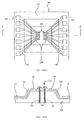
- the probe card A shown in Fig. 1 and Fig. 2 is a sensing part of a measuring device (not shown) for measuring an object to be measured (not shown), and comprises: a supporting substrate 100; probes 200 to be arranged on one surface of the supporting substrate 100; and a main substrate 300 disposed opposite to the other surface of the supporting substrate 100.
- a measuring device not shown
- the probe card A shown in Fig. 1 and Fig. 2 is a sensing part of a measuring device (not shown) for measuring an object to be measured (not shown), and comprises: a supporting substrate 100; probes 200 to be arranged on one surface of the supporting substrate 100; and a main substrate 300 disposed opposite to the other surface of the supporting substrate 100.
- a silicon substrate is used for the supporting substrate 100.
- the one surface of the supporting substrate 100 has been formed into a pyramid shape having one step (i.e. convex shape) by anisotropic etching. This step part of the one surface of the supporting substrate 100 is sloped.
- a grand layer 101, an insulating layer 102 and wiring patterns 120 are sequentially stacked to be formed by vapor deposition, plating, etching or the like.
- the thick part of the supporting substrate 100 has a thickness of 500 to 1500 ⁇ m while the thin part thereof is 100 to 500 ⁇ m.
- a plurality of probes 200 are arranged in two rows at a prescribed pitch spacing.
- the probes 200 in the respective rows are opposed to each other.
- a plurality of bumps 110 are arranged at a wider pitch spacing than the probes 200.
- the probes 200 and the bumps 110 are electrically connected with each other via the plurality of wiring patterns 120.
- a ground layer 101, an insulating layer 102 and the wiring patterns 120 are sequentially stacked on the one surface of the supporting substrate 100, to constitute microstrip lines.
- the insulating layer 102 on the supporting substrate 100 is provided with a circuit element 103 electrically connected with the wiring patterns 120.
- This circuit element 103 is an element necessary in electrical measurement using the probes 200, and herein, a capacitor, which functions as a so-called "passcon” (bypass capacitor), and the circuit element, which functions as BOST (Build Out Self Test) for aiding a test (namely, measurement of electric characteristics of an object B to be measured), are used.
- the capacitor serves to promote improvement in high frequency characteristics.
- the circuit element, having the function as BOST serves in a varying manner depending on the contents of the test on the object B to be measured.
- a light-sensitive film is applied to the wiring patterns 120 on the thick part of the supporting substrate 100, a pattern is formed on this light-sensitive film to be plated, which is repeated to integrally form the probes 200 on the wiring patterns 120.
- each of the probes 200 is formed to have a first one-quarter arc part 210 with the one end thereof supported by the insulating layer 102, and a second one-quarter arc 220 connected with the other end of the first one-quarter arc part 210, and made slightly shorter than the first one-quarter arc part 210.
- the tops of the probes 200 are contact parts to come into contact with the electrode of the object to be measured.
- the main substrate 300 is a substrate to be mounted in a state of being in contact with the supporting substrate 100, and a printed circuit board is used here.
- a plurality of through holes 310 filled with a conductive material 311 are formed in the main substrate 300.
- a plurality of bumps 320 are connected with the bumps 110 of the supporting substrate 100 via a flexible substrate 400.
- each of wiring patterns 330 to be electrically connected with the conductive material 311 in the through holes 310 are formed on the other surface of the main substrate 300.
- the other ends of the wiring patterns 330 are electrically connected with an outer electrode which is not shown, and the wiring patterns 330 are electrically connected to the measuring device through this outer electrode.
- a signal outputted from the measuring device is transmitted through the outer electrode, the wiring patterns 330, the conductive material 311, the bumps 320, the flexible substrate 400, the bumps 110, the wiring patterns 120, and the probes 200, sequentially.
- the main substrate 300 of as thus constituted is mounted on a prober of the measuring device, and the probe card A is then used for measurement of electrical characteristics of the object to be measured. A method of use thereof is specifically described below.
- a probe-driving device is activated, and the supporting substrate 100 and the object to be measured are made relatively close to each other. This brings the tops of the probes 200 into contact with the electrode of the object to be measured. Subsequently, the supporting substrate 100 and the object to be measured are further made relatively close to each other so that the probes 200 are pressed by the electrode of the object to be measured (namely, overdrive is executed). At this time, since the probes 200 are arranged on the thick part of the supporting substrate 100, the supporting substrate 100 is not warped under the pressing force acted through the probes 200.
- the top of the second one-quarter arc 220 in each of the probes 200 comes into contact with the surface of the supporting substrate 100, as shown in Fig. 3, and then moves (in the arrow direction of Fig.3) on the surface of the supporting substrate 100. Simultaneously, the tops of the probes 200 slide on the electrode of the object to be measured. It is thereby possible to secure the prescribed contact pressure necessary for conducting electricity between the probes 200 and the electrode of the object to be measured, as well as a prescribed amount scrubbed, so that stable contact can be promoted.
- the supporting substrate 100 is not warped under the pressing force that acts through the probes 200 when the probes 200 and the electrode of the object to be measured are brought into contact with each other. This enables stable measurement.
- the one surface of the supporting substrate 100 is formed in a pyramid shape having one step and the probes 200 are arranged on the surface of the thick part (namely, on the surface of the top step) while the bumps 110 are arranged on the surface of the thin part (namely, on the surface of the lower steps), when the probes 200 comes into contact with the electrode of the object to be measured, the bumps 110 are not brought into contact with the object to be measured. Namely, even if the integration of the object to be measured is increased and the probes 200 are made finer associated with the increased integration, the bumps 110 are not arranged in a higher position than the probes 200, thereby enabling sufficient correspondence to the object to be measured.
- the one surface of the supporting substrate 100 is formed in a pyramid shape having one step, it may be formed in a convex shape having one or more steps, and may for example be formed in a staircase shape.
- the ground layer 101 and the insulating layer 102 are sequentially stacked on the supporting substrate 100, those layers are not necessarily arranged.
- the bumps 110, the wiring patterns 120 and the probes 200 are formed on the one surface of the supporting substrate 100.
- the bumps 110 may be arranged on the surface of any of lower steps.
- the supporting substrate 100 is a silicon substrate, it is possible, naturally, to use another substrate.
- through holes 105 with ⁇ 50 to 100 ⁇ m can be formed in the thick part of the supporting substrate 100.
- the through holes 105 are formed from the surface of the top step in the one surface of the supporting substrate 100 through the other surface of the supporting substrate 100.
- each of probes 500 for connection is inserted into each of the through holes 105.
- each of the through holes 105 is arranged between the probes 200, as shown in Fig. 4(b). Namely, the front end of each of the probes 500 for connection protrudes from between the probes 200 to come into contact with the electrode for power source of the object to be measured while the back end thereof is electrically connected with the measuring device.
- the through holes 105 are formed in such a position that the probes 500 for connection are electrically connectable with the wiring patterns 120. While being in contact with the wiring patterns 120, the probes 500 for connection come into contact with wiring patterns (not shown) on the one surface of the main substrate 300, to electrically connect the main substrate 300 with the wiring patterns 120. Further, as shown in Fig. 5, a cylindrical concave part 106 may be arranged in the other surface of the thick part of the supporting substrate 100, followed by formation of the through holes 105 from the concave part 106. This arrangement can facilitate formation of the through holes 105.
- the probes 500 for connection are configured to be springy so as to come into contact with the electrode of the object to be measured, the wiring patterns 120 or the wiring patterns on the main substrate 300, by prescribed contact pressure.
- the probes 500 can include springs or the like therebetween, or be provided with a bent part (cf. Fig. 5).
- the shape of the probes 200 to be used is not limited to the forgoing shape of the example, and may be any shape.
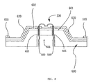
- a probe card A' shown in Fig. 6 comprises a supporting substrate 600 and a plurality of probes 200 arranged on the supporting substrate 600.
- This probe card A' and the probe card A have almost the same configuration, but are different in that a plurality of through holes 630 (first through holes) are formed in the thin part of the supporting substrate 600. In the following, this difference is described in detail whereas explanations of the overlapped parts are omitted.
- the supporting substrate 600 has almost the same configuration as that of the supporting substrate 100, except that the through holes 630 are formed in the thin part, and that bumps 610 are arranged in such a position as can come into contact with a conductive material 631 in the through holes 630 on the other surface, not the one surface, of the supporting substrate 600. Holes with ⁇ 50 to 100 ⁇ m are formed from the surface of the lower steps in the one surface of the supporting substrate 600 through the other surface of the supporting substrate 600, which are then filled with the conductive material 631, to constitute the through holes 630.
- a ground layer 601, an insulating layer 602 and the wiring patterns 620 are sequentially formed on the one surface of the supporting substrate 600.
- the conductive material 631 in the through holes 630 electrically connects the ground layer 601 with the bumps 610.
- the ground layer 601 and the wiring patterns 620 are electrically connected with each other by vapor deposition of the wiring patterns 620 on an opening formed in the insulating layer 602.
- a signal outputted from the measuring device is transmitted through the outer electrode (not shown) of the main substrate 300, the wiring patterns 330, the conductive material 311, the bumps 320, the bumps 610, the conductive material 631, the ground layer 601, the wiring patterns 620, and the probes 200, sequentially.
- the main substrate 300 of the probe card A' as thus constituted is mounted on the prober of the measuring device, and the probe card A' is then used for measurement of electrical characteristics of the object to be measured. A using method thereof is specifically described below.
- a probe-driving device is activated, and the supporting substrate 600 and the object to be measured are made relatively close to each other. This brings the tops of the probes 200 into contact with the electrode of the object to be measured. Subsequently, the supporting substrate 600 and the object to be measured are further made relatively close to each other so that the probes 200 are pressed by the electrode of the object to be measured (namely, overdrive is executed). At this time, since the probes 200 are arranged on the thick part of the supporting substrate 600, the supporting substrate 600 is not warped under pressing force acted through the probes 200.
- the top of the second one-quarter arc 220 in each of the probes 200 comes into contact with the surface of the supporting substrate 600, and then moves on the surface of the supporting substrate 600. Simultaneously, the tops of the probes 200 slide on the electrode of the object to be measured. It is thereby possible to secure prescribed contact pressure necessary for conducting electricity between the probes 200 and the electrode of the object to be measured, as well as a prescribed amount scrubbed, so that stable contact can be promoted.
- the same effect as that of the probe card A is exerted.
- a thin part is provided in the supporting substrate 600 by forming the one surface of the supporting substrate 600 into a pyramid shape having one step, it is possible to readily form the through holes 630 by forming the through holes 630 in the thin part. Namely, the process time for forming the through holes 630 is substantially reduced as compared to conventional examples, which can lower the operation cost to promote cost reduction.
- the supporting substrate 600 and the main substrate 300 can be electrically connected with each other only by mounting the supporting substrate 600 on the main substrate 300, which is readily conducted as compared with the case like the probe card A where the flexible substrate 400 is used for electrical connection. That is, also from this aspect, the operation time can be reduced because the probe card A' can be readily assembled, thereby to promote cost reduction.
- the one surface of the supporting substrate 600 is formed in a pyramid shape having one step, it may be formed in a convex shape having one or more steps, and may for example be formed in a staircase shape.
- the ground layer 601 and the insulating layer 602 are sequentially stacked on this supporting substrate 600, those are not necessarily arranged.
- the supporting substrate 600 is a silicon substrate, it is possible, naturally, to use another substrate.
- through holes 605 with ⁇ 50 to 100 ⁇ m can be formed in the thick part of the supporting substrate 600.
- the through holes 605 are formed from the surface of the top step in the one surface of the supporting substrate 600 through the other surface of the supporting substrate 600.
- each of the probes 500 for connection is inserted into each of the through holes 605.
- each of the through holes 605 is arranged between the probes 200. Namely, the front end of each of the probes 500 for connection protrudes from between the probes 200 to come into contact with the electrode for power source of the object to be measured while the back end thereof is electrically connected with the measuring device.
- the through holes 605 are formed in such a position that the probes 500 for connection are electrically connectable with the wiring patterns 620. Namely, while being in contact with the wiring patterns 620, the probes 500 for connection come into contact with wiring patterns (not shown) on the one surface of the main substrate 300, to electrically connect the supporting substrate 600 with the main substrate 300. Further, as shown in Fig. 8, a cylindrical concave part 606 may be arranged in the other surface of the thick part of the supporting substrate 600, followed by formation of the through holes 605 from the concave part 606. This arrangement can facilitate formation of the through holes 605.
- the probes 500 for connection are configured to be springy so as to come into contact with the electrode of the object to be measured, the wiring patterns 620 or the wiring patterns on the main substrate 300, by prescribed contact pressure.
- the probes 500 can include springs or the like therebetween, or be provided with a bent part (c.f. Fig. 8).
- the through holes 630 are configured to be filled with the conductive material 631
- the conductive material 631 may be plated on the inner wall of the through holes 630 so as to electrically connect the bumps 610 with the ground layer 601 through the conductive material 631 on the inner wall.
- the shape of the probes 200 to be used is not limited to the forgoing shape of the example, and may be any shape.
- the main substrate 300 can be mounted on the supporting substrate 100 or the supporting substrate 600 in a contacting state, it is possible, naturally, that the main substrate 300 is connected with the supporting substrate 100 or the supporting substrate 600 in a separate state via a supporting member such as a threaded rod.
Landscapes
- Health & Medical Sciences (AREA)
- Engineering & Computer Science (AREA)
- Biomedical Technology (AREA)
- Life Sciences & Earth Sciences (AREA)
- Public Health (AREA)
- Veterinary Medicine (AREA)
- General Health & Medical Sciences (AREA)
- Animal Behavior & Ethology (AREA)
- Radiology & Medical Imaging (AREA)
- Nuclear Medicine, Radiotherapy & Molecular Imaging (AREA)
- Physics & Mathematics (AREA)
- Heart & Thoracic Surgery (AREA)
- Pathology (AREA)
- General Physics & Mathematics (AREA)
- Biophysics (AREA)
- Vascular Medicine (AREA)
- Physical Education & Sports Medicine (AREA)
- Optics & Photonics (AREA)
- Measuring Leads Or Probes (AREA)
- Testing Or Measuring Of Semiconductors Or The Like (AREA)
Applications Claiming Priority (2)
| Application Number | Priority Date | Filing Date | Title |
|---|---|---|---|
| JP2004047657A JP2005241275A (ja) | 2004-02-24 | 2004-02-24 | プローブカード |
| JP2004047657 | 2004-02-24 |
Publications (2)
| Publication Number | Publication Date |
|---|---|
| EP1569000A2 true EP1569000A2 (de) | 2005-08-31 |
| EP1569000A3 EP1569000A3 (de) | 2006-05-03 |
Family
ID=34747434
Family Applications (1)
| Application Number | Title | Priority Date | Filing Date |
|---|---|---|---|
| EP05250976A Withdrawn EP1569000A3 (de) | 2004-02-24 | 2005-02-21 | Nadelkarte |
Country Status (6)
| Country | Link |
|---|---|
| US (1) | US20050184743A1 (de) |
| EP (1) | EP1569000A3 (de) |
| JP (1) | JP2005241275A (de) |
| KR (1) | KR20060042168A (de) |
| CN (1) | CN1661376A (de) |
| TW (1) | TW200533924A (de) |
Families Citing this family (20)
| Publication number | Priority date | Publication date | Assignee | Title |
|---|---|---|---|---|
| USRE43503E1 (en) | 2006-06-29 | 2012-07-10 | Microprobe, Inc. | Probe skates for electrical testing of convex pad topologies |
| US7759949B2 (en) | 2004-05-21 | 2010-07-20 | Microprobe, Inc. | Probes with self-cleaning blunt skates for contacting conductive pads |
| US9476911B2 (en) | 2004-05-21 | 2016-10-25 | Microprobe, Inc. | Probes with high current carrying capability and laser machining methods |
| US8988091B2 (en) | 2004-05-21 | 2015-03-24 | Microprobe, Inc. | Multiple contact probes |
| US9097740B2 (en) | 2004-05-21 | 2015-08-04 | Formfactor, Inc. | Layered probes with core |
| US7649367B2 (en) | 2005-12-07 | 2010-01-19 | Microprobe, Inc. | Low profile probe having improved mechanical scrub and reduced contact inductance |
| JP2007248322A (ja) * | 2006-03-17 | 2007-09-27 | Japan Electronic Materials Corp | プローブカード |
| US7312617B2 (en) * | 2006-03-20 | 2007-12-25 | Microprobe, Inc. | Space transformers employing wire bonds for interconnections with fine pitch contacts |
| US8907689B2 (en) | 2006-10-11 | 2014-12-09 | Microprobe, Inc. | Probe retention arrangement |
| US7514948B2 (en) | 2007-04-10 | 2009-04-07 | Microprobe, Inc. | Vertical probe array arranged to provide space transformation |
| JP2008275409A (ja) * | 2007-04-27 | 2008-11-13 | Alps Electric Co Ltd | プローブカード |
| CN101329365B (zh) * | 2007-06-21 | 2010-09-22 | 均扬电子有限公司 | 探针卡及其组合装配方法 |
| US8723546B2 (en) | 2007-10-19 | 2014-05-13 | Microprobe, Inc. | Vertical guided layered probe |
| US8230593B2 (en) | 2008-05-29 | 2012-07-31 | Microprobe, Inc. | Probe bonding method having improved control of bonding material |
| JP5374079B2 (ja) * | 2008-06-20 | 2013-12-25 | 東京エレクトロン株式会社 | 検査用接触構造体 |
| JP2011043377A (ja) * | 2009-08-20 | 2011-03-03 | Tokyo Electron Ltd | 検査用接触構造体 |
| JP2016191563A (ja) * | 2015-03-30 | 2016-11-10 | 株式会社東芝 | プローブカード及びそれを含む試験装置 |
| CN114200278B (zh) * | 2021-11-29 | 2022-12-27 | 强一半导体(苏州)有限公司 | 一种薄膜探针卡及其探针头 |
| CN114200279B (zh) * | 2021-11-29 | 2023-03-14 | 强一半导体(苏州)有限公司 | 一种薄膜探针卡及其探针头 |
| CN114200280B (zh) * | 2021-11-29 | 2022-11-15 | 强一半导体(苏州)有限公司 | 一种薄膜探针卡及其探针头 |
Family Cites Families (22)
| Publication number | Priority date | Publication date | Assignee | Title |
|---|---|---|---|---|
| US5090118A (en) * | 1990-07-31 | 1992-02-25 | Texas Instruments Incorporated | High performance test head and method of making |
| US5225037A (en) * | 1991-06-04 | 1993-07-06 | Texas Instruments Incorporated | Method for fabrication of probe card for testing of semiconductor devices |
| US5786701A (en) * | 1993-07-02 | 1998-07-28 | Mitel Semiconductor Limited | Bare die testing |
| US5483741A (en) * | 1993-09-03 | 1996-01-16 | Micron Technology, Inc. | Method for fabricating a self limiting silicon based interconnect for testing bare semiconductor dice |
| US5497103A (en) * | 1995-01-25 | 1996-03-05 | International Business Machines Corporation | Test apparatus for circuitized substrate |
| US5777379A (en) * | 1995-08-18 | 1998-07-07 | Tessera, Inc. | Semiconductor assemblies with reinforced peripheral regions |
| US6211572B1 (en) * | 1995-10-31 | 2001-04-03 | Tessera, Inc. | Semiconductor chip package with fan-in leads |
| US5869974A (en) * | 1996-04-01 | 1999-02-09 | Micron Technology, Inc. | Micromachined probe card having compliant contact members for testing semiconductor wafers |
| US5834945A (en) * | 1996-12-31 | 1998-11-10 | Micron Technology, Inc. | High speed temporary package and interconnect for testing semiconductor dice and method of fabrication |
| US6060891A (en) * | 1997-02-11 | 2000-05-09 | Micron Technology, Inc. | Probe card for semiconductor wafers and method and system for testing wafers |
| US6040618A (en) * | 1997-03-06 | 2000-03-21 | Micron Technology, Inc. | Multi-chip module employing a carrier substrate with micromachined alignment structures and method of forming |
| US6025730A (en) * | 1997-03-17 | 2000-02-15 | Micron Technology, Inc. | Direct connect interconnect for testing semiconductor dice and wafers |
| US6040239A (en) * | 1997-08-22 | 2000-03-21 | Micron Technology, Inc. | Non-oxidizing touch contact interconnect for semiconductor test systems and method of fabrication |
| US6018249A (en) * | 1997-12-11 | 2000-01-25 | Micron Technolgoy, Inc. | Test system with mechanical alignment for semiconductor chip scale packages and dice |
| US6130148A (en) * | 1997-12-12 | 2000-10-10 | Farnworth; Warren M. | Interconnect for semiconductor components and method of fabrication |
| US6552555B1 (en) * | 1998-11-19 | 2003-04-22 | Custom One Design, Inc. | Integrated circuit testing apparatus |
| US6242932B1 (en) * | 1999-02-19 | 2001-06-05 | Micron Technology, Inc. | Interposer for semiconductor components having contact balls |
| JP4388620B2 (ja) * | 1999-04-16 | 2009-12-24 | 株式会社アドバンテスト | プローブカード及びプローブカード製造方法 |
| US6263566B1 (en) * | 1999-05-03 | 2001-07-24 | Micron Technology, Inc. | Flexible semiconductor interconnect fabricated by backslide thinning |
| JP2001033487A (ja) * | 1999-07-22 | 2001-02-09 | Mitsubishi Electric Corp | 半導体集積回路テスト用のプローブカードおよびこのプローブカードの製造方法 |
| JP4480258B2 (ja) * | 2000-03-29 | 2010-06-16 | 株式会社日本マイクロニクス | 半導体デバイス検査装置における電気的接触装置 |
| US7002225B2 (en) * | 2002-05-24 | 2006-02-21 | Northrup Grumman Corporation | Compliant component for supporting electrical interface component |
-
2004
- 2004-02-24 JP JP2004047657A patent/JP2005241275A/ja not_active Withdrawn
-
2005
- 2005-02-14 US US11/056,278 patent/US20050184743A1/en not_active Abandoned
- 2005-02-17 TW TW094104630A patent/TW200533924A/zh unknown
- 2005-02-21 EP EP05250976A patent/EP1569000A3/de not_active Withdrawn
- 2005-02-22 CN CN200510007499XA patent/CN1661376A/zh active Pending
- 2005-02-24 KR KR1020050015481A patent/KR20060042168A/ko not_active Withdrawn
Also Published As
| Publication number | Publication date |
|---|---|
| CN1661376A (zh) | 2005-08-31 |
| JP2005241275A (ja) | 2005-09-08 |
| KR20060042168A (ko) | 2006-05-12 |
| EP1569000A3 (de) | 2006-05-03 |
| US20050184743A1 (en) | 2005-08-25 |
| TW200533924A (en) | 2005-10-16 |
Similar Documents
| Publication | Publication Date | Title |
|---|---|---|
| US20050184743A1 (en) | Probe card | |
| US5973394A (en) | Small contactor for test probes, chip packaging and the like | |
| US7244125B2 (en) | Connector for making electrical contact at semiconductor scales | |
| US5829988A (en) | Socket assembly for integrated circuit chip carrier package | |
| US6922069B2 (en) | Needle assembly of probe card | |
| US6774654B2 (en) | Semiconductor-device inspecting apparatus and a method for manufacturing the same | |
| US20050184745A1 (en) | Probe card | |
| JPH09281144A (ja) | プローブカードとその製造方法 | |
| US7888953B2 (en) | Probe card | |
| CA2358405A1 (en) | Text probe interface assembly and manufacture method | |
| US7504839B2 (en) | Flexible circuit with micro-sized probe tips and a method of making the same | |
| KR100473584B1 (ko) | 외팔보 형태의 프로브 카드 및 그 제조 방법 | |
| JPH09199247A (ja) | ソケット | |
| KR100523745B1 (ko) | 전자소자 검사용 마이크로 프로브 및 그 제조 방법 | |
| US6674297B1 (en) | Micro compliant interconnect apparatus for integrated circuit devices | |
| TWI266057B (en) | Integrated probe card and the packaging method | |
| EP1943528A1 (de) | Nadelkarte mit gestapeltem substrat | |
| KR100340754B1 (ko) | 커넥터 장치 | |
| US7293995B2 (en) | Electrical contact and connector system | |
| JP2010043898A (ja) | 配線基板、ic電気特性検査用配線基板、及び配線基板の製造方法 | |
| US6667627B2 (en) | Probe for inspecting semiconductor device and method of manufacturing the same | |
| US20190391180A1 (en) | Connector having contact members | |
| KR100473430B1 (ko) | 수직형 프로브 카드 | |
| KR101112749B1 (ko) | 반도체 디바이스 테스트 소켓 및 그 제조 방법 | |
| KR100595373B1 (ko) | 브릿지 형태의 프로브 카드 및 그 제조 방법 |
Legal Events
| Date | Code | Title | Description |
|---|---|---|---|
| PUAI | Public reference made under article 153(3) epc to a published international application that has entered the european phase |
Free format text: ORIGINAL CODE: 0009012 |
|
| AK | Designated contracting states |
Kind code of ref document: A2 Designated state(s): AT BE BG CH CY CZ DE DK EE ES FI FR GB GR HU IE IS IT LI LT LU MC NL PL PT RO SE SI SK TR |
|
| AX | Request for extension of the european patent |
Extension state: AL BA HR LV MK YU |
|
| PUAL | Search report despatched |
Free format text: ORIGINAL CODE: 0009013 |
|
| AK | Designated contracting states |
Kind code of ref document: A3 Designated state(s): AT BE BG CH CY CZ DE DK EE ES FI FR GB GR HU IE IS IT LI LT LU MC NL PL PT RO SE SI SK TR |
|
| AX | Request for extension of the european patent |
Extension state: AL BA HR LV MK YU |
|
| STAA | Information on the status of an ep patent application or granted ep patent |
Free format text: STATUS: THE APPLICATION HAS BEEN WITHDRAWN |
|
| 18W | Application withdrawn |
Effective date: 20061107 |