EP1566935A1 - Dispositif et procédé de suppression d'interférences impulsionnelles dans un signal - Google Patents
Dispositif et procédé de suppression d'interférences impulsionnelles dans un signal Download PDFInfo
- Publication number
- EP1566935A1 EP1566935A1 EP05101201A EP05101201A EP1566935A1 EP 1566935 A1 EP1566935 A1 EP 1566935A1 EP 05101201 A EP05101201 A EP 05101201A EP 05101201 A EP05101201 A EP 05101201A EP 1566935 A1 EP1566935 A1 EP 1566935A1
- Authority
- EP
- European Patent Office
- Prior art keywords
- signal
- successive
- coefficient
- values
- duration
- Prior art date
- Legal status (The legal status is an assumption and is not a legal conclusion. Google has not performed a legal analysis and makes no representation as to the accuracy of the status listed.)
- Granted
Links
- 238000000034 method Methods 0.000 title claims abstract description 14
- 230000001629 suppression Effects 0.000 title description 16
- 238000012937 correction Methods 0.000 claims abstract description 17
- 238000005070 sampling Methods 0.000 claims description 18
- 238000001514 detection method Methods 0.000 claims description 13
- 238000012545 processing Methods 0.000 claims description 12
- 101100316754 Arabidopsis thaliana VAL3 gene Proteins 0.000 claims description 4
- 230000003068 static effect Effects 0.000 abstract 1
- 230000005540 biological transmission Effects 0.000 description 7
- 239000000969 carrier Substances 0.000 description 5
- 230000007774 longterm Effects 0.000 description 5
- 230000004044 response Effects 0.000 description 5
- 101100316752 Arabidopsis thaliana VAL1 gene Proteins 0.000 description 4
- 101100316753 Arabidopsis thaliana VAL2 gene Proteins 0.000 description 4
- 238000001228 spectrum Methods 0.000 description 4
- 230000002123 temporal effect Effects 0.000 description 3
- XUIMIQQOPSSXEZ-UHFFFAOYSA-N Silicon Chemical compound [Si] XUIMIQQOPSSXEZ-UHFFFAOYSA-N 0.000 description 2
- 101000771022 Trichoderma longibrachiatum Chlorophenol O-methyltransferase Proteins 0.000 description 2
- 238000010586 diagram Methods 0.000 description 2
- 229910052710 silicon Inorganic materials 0.000 description 2
- 239000010703 silicon Substances 0.000 description 2
- 238000007792 addition Methods 0.000 description 1
- 230000015556 catabolic process Effects 0.000 description 1
- 238000006243 chemical reaction Methods 0.000 description 1
- 238000006731 degradation reaction Methods 0.000 description 1
- 238000000605 extraction Methods 0.000 description 1
- 238000002955 isolation Methods 0.000 description 1
- 238000004080 punching Methods 0.000 description 1
- 230000002441 reversible effect Effects 0.000 description 1
- 230000035945 sensitivity Effects 0.000 description 1
- 238000006467 substitution reaction Methods 0.000 description 1
- 238000012549 training Methods 0.000 description 1
- 238000012546 transfer Methods 0.000 description 1
- 230000009466 transformation Effects 0.000 description 1
- 230000017105 transposition Effects 0.000 description 1
Images


Classifications
-
- H—ELECTRICITY
- H04—ELECTRIC COMMUNICATION TECHNIQUE
- H04L—TRANSMISSION OF DIGITAL INFORMATION, e.g. TELEGRAPHIC COMMUNICATION
- H04L27/00—Modulated-carrier systems
- H04L27/26—Systems using multi-frequency codes
- H04L27/2601—Multicarrier modulation systems
- H04L27/2647—Arrangements specific to the receiver only
Definitions
- the present invention relates to a device and a method of suppressing impulse interference contained in a signal.
- the present invention relates to a device and method for suppressing impulse interference for a COFDM type demodulator ("Coded Orthogonal Frequency Division Multiplex "or Division Multiplexing coded orthogonal frequency).
- data packets emit are put in the form of N complex coefficients associated with N respective frequencies (or carriers).
- the number N frequencies is for example equal to 1705 for the so-called “2K” mode and 6817 for the so-called “8K” mode, in wireless transmission of Digital TV.
- the set of these N coefficients is processed by inverse fast Fourier transform (IFFT), which produces a "symbol” consisting of a sum of modulated carriers, each carrier having an amplitude and a phase determined by the associated complex coefficient. The symbol thus generated is issued.
- IFFT inverse fast Fourier transform
- the useful life is of the order of 224 ⁇ s in 2K mode and 896 ⁇ s in 8K mode, for a bandwidth of 8 MHz.
- a receiver makes the symbol reverse treatment, that is to say mainly a transformed Fourier Fast (FFT) to reconstruct the coefficients starting complexes.
- FFT transformed Fourier Fast
- pilots Some carriers of the modulated signal, called pilots, are used during the demodulation for determine an estimate of the frequency response of the channel of transmission used and to carry out the transformation of Fast Fourier modulated signal.
- the signal received by the COFDM demodulator corresponds to modulated transmitted signal modified by disturbances of origins variety. It is therefore necessary to correct the received signal for find the transmitted symbols.
- the transmission noise usually corresponds to a low-energy disturbance that is present permanently and which is characteristic of the canal transmitted by the signal between the receiver and the transmitter.
- impulse interference correspond to very short disturbances in duration but which have a high energy. These are disturbances that are not neither reproducible nor predictable, which are not present time, and that can occur in isolation or in groups at any time with amplitude, duration, and unpredictable start times. Interference impulses are, for example, due to equipment located near the demodulator components.
- Correction of transmission noise generally uses temporal stability properties such a disturbance.
- Correction of impulse interference generally employs a method of individually detect each impulse interference and correcting the modulated signal received when impulse interference is detected.
- An example of a method of detection and correction of classical impulse interference is the threshold detection method with zero substitution.
- a such a method is, for example, implemented on the demodulator reference STV0360, marketed by the Applicant. he is to detect the presence of impulse interference comparing, at a given comparison point, the amplitude a digital modulated signal obtained by analog-to-digital conversion the analog modulated signal received by the demodulator, usually after a frequency change to a range of intermediate frequencies. All numerical values of the digital modulated signal greater than the determined threshold are replaced by a predetermined value, for example the value average of the signal.
- the main difficulty of threshold detection is the choice of the comparison threshold. Indeed, if the threshold is too high, only impulse interference at very high energy are detected and impulse interference from a lower energy level may not be detected. Conversely, if the detection threshold is too low, a part of the digital modulated signal undisturbed by Impulse interference can be suppressed.
- the present invention provides a device and a method of suppressing disturbing impulse interference a signal, in particular a signal received by a demodulator COFDM, allowing suppression of impulse interference at high energy, but also impulse interferences moderate energy, while limiting the risk of inaccurate detection of impulse interference.
- the present invention provides a device for suppressing impulse interference contained in a signal, comprising a detection circuit impulse interference contained in the signal, and a signal correction circuit disturbed by interference detected pulses, in which the circuit of detection comprises a circuit for determining a first coefficient representative of a statistical characteristic of the evolution of the signal on a first duration; a circuit of determining a second coefficient representative of a statistical characteristic of the evolution of the signal on a second duration greater than the first duration; and a circuit of comparison comparing the first and second coefficients and providing a signal indicative of the presence of a impulse interference on the first duration when the first coefficient differs significantly from the second coefficient.
- the circuit determining the first coefficient determines the first coefficient from the absolute values of numerical values successive samples obtained by sampling the signal during first duration and the determination circuit of the second coefficient determines the second coefficient from the values absolute values of successive numerical values obtained by signal sampling during the second duration.
- the circuit for determining the first coefficient provides the sum absolute values of successive numerical values obtained by sampling the signal during the first duration, each absolute value of numerical value greater than a threshold determined by being replaced by a weighting constant greater than or equal to the threshold.
- the circuit for determining the first coefficient comprises a first entry receiving first numeric values successive ones resulting from the sampling of the signal; a second input receiving second successive numerical values from temporally offset signal sampling compared to the first successive numerical values of the first duration; a first processing circuit connected to the first input and adapted to provide third values numerical values corresponding to the absolute values of first successive numerical values, each absolute value a first numerical value greater than the threshold being replaced by the weighting constant; a second circuit of processing connected to the second input and adapted to provide fourth successive numerical values corresponding to the absolute values of the second successive numerical values, each absolute value of a second upper numerical value the threshold being replaced by the weighting constant; a subtractor connected to the first and second weighting circuits and successively supplying fifth numerical values successive amounts corresponding to the subtraction between the fourth successive numerical values and the third values successive numerals; and an adder whose first input receives the fifth numerical values and one of which second input is connected to the output of the adder and providing corresponding sixth consecutive numerical values at the first
- the constant weighting is greater than or equal to three times the threshold.
- the circuit of determination of the second coefficient comprises a receiving input first successive numerical values from signal sampling; a processing circuit connected to the input and adapted to provide second numerical values corresponding to the absolute values of the first successive numerical values, each absolute value of a first numerical value greater than a threshold being replaced by a weighting constant less than or equal to the threshold; an adder whose first entry receives the second successive numerical values and of which a second entry is connected to the output of the adder and providing third successive numerical values; and a circuit receiving the third successive numerical values and providing fourth successive numerical values, corresponding to the second coefficient, equal to the third successive numerical values multiplied by the ratio between the first duration and the second duration.
- the second input of the adder receives the value zero during a cycle operation of the adder after a determined number of successive cycles of operation equivalent to the second duration.
- the third successive numerical values are multiplied by one corrective coefficient greater than or equal to 2.
- the present invention also provides a method of suppression of impulse interference contained in a signal, comprising a step of detecting interference pulses contained in the signal, and a step of correction of detected impulse interferences in which the detecting step comprises a determining step a first coefficient representative of a characteristic statistic of the evolution of the signal on a first duration and a second coefficient representative of a characteristic statistical evolution of the signal over a second duration greater than the first duration; and a step of detecting the presence of impulse interference on the signal by comparing the first and second coefficients.
- the first coefficient is the sum of the absolute values, possibly corrected, successive numerical values obtained by sampling the signal during the first duration and in which the second coefficient corresponds to the sum of absolute values, possibly corrected values successive numerals obtained by sampling the signal during the second duration.
- the present invention will now be described for a COFDM demodulator. It is clear that the present invention finds application for any type of treatment system a signal disturbed by impulse interferences that one wish to correct.
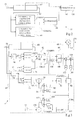
- FIG. 1 shows, in more detail, an example of COFDM demodulator according to the invention.
- An E input of the demodulator receives an intermediate frequency IF signal sampling, for example 36 MHz.
- IF signal corresponds to the signal received after various changes or transpositions frequency.
- Input E is coupled to an analog-to-digital converter 10 (ADC) which digitizes the IF input signal.
- ADC analog-to-digital converter 10
- the analog / digital converter 10 provides an IS signal to a module 11 for suppressing impulse interference.
- the module 11 provides an OS signal corresponding to the signal signed IS in which the impulse interferences are suppressed.
- the module 11 attacks a module 12 of frequency change.
- the module 12 provides a signal substantially in baseband, the signal spectrum at the output of the module 12 being centered on a frequency substantially equal to zero.
- Module 12 is coupled to a module 14 allowing on the one hand a fine adjustment of the frequency signal spectrum and, on the other hand, provide temporal samples at times appropriate to the further processing.
- the spectrum of signal is centered on a frequency equal to 0 and the number and the temporal position of the samples are suitable for processing by Fourier transform that takes place in the module next.
- the module 14 is controlled by links 15 and 15 ' connecting the module 14 to a module 16 for processing pilots.
- the output of the module 14 attacks a module 20 of Fast Fourier Transform (FFT) which provides the frequencies corresponding to a symbol.
- FFT Fast Fourier Transform
- the module 20 is driven by a module 22 which provides, via a link 24, a signal of adjustment of the analysis window of the transform of Fourier.
- module 20 The output of module 20 is coupled to module 16 which performs extraction and processing of pilots.
- the module 16 provides on the links 15 and 15 'the signals intended for correct the center frequency of the spectrum and the frequency signal sampling.
- the output of the module 20 attacks a module 30 in which the signal is corrected using an estimate of the Frequency response of the channel.
- the estimation of the frequency response of the channel is carried out in module 16 using the drivers. This estimate is provided by module 16 on a link 55, a branch 55a of which is coupled to the module 30.
- output of the module 30, the signal comprises in particular the carriers conveying the data.
- the estimation of the frequency response of the channel, provided by module 16, feeds, via the link 55 and a branch 55b of the link 55, a module 26 inverse Fourier transform (IFFT), to determine the impulse response of the channel.
- Module 26 provides the answer impulse channel to module 22, to dynamically adjust the positioning of the FFT analysis window.
- the processing of the carriers carrying the data is provided in a circuit 40 for processing and providing data.
- the circuit 40 has a conventional structure and may include, as this is represented in FIG. 4, a deinterlacing module 42 of symbols, a module 44 called “demapping", a module 46 of deinterleaving bits, and a module 48 (FEC) of error correction.
- the output of module 48 constitutes the output S of the circuit 40 and the demodulator and provides data corresponding to the data sent.
- the module 22 receives the signal output of the module 14 by a link 54, to roughly adjust the analysis window.
- FIG. 2 schematically represents an example of implementation of the impulse interference suppression module 11 according to the invention.
- the module 11 receives the signal IS in output of the analog / digital converter 10, and provides the OS output signal that attacks the signal transfer module in baseband 12.
- the module 11 includes a memory 60 adapted to store simultaneously the last N successive numerical values of the input signal IS received by the module 11, N being example, an even natural integer of the order of 32 to 64.
- N being example, an even natural integer of the order of 32 to 64.
- the module 11 comprises a determination module 62 a coefficient COEFF1 representative of the evolution of the signal IS input for the last N digital values of the IS signal received, henceforth called short evolution coefficient duration, which, for example, simultaneously receives the value of the signal IS of time t0 and the numerical value of the signal IS of instant tN stored in memory 60 or which receives all the values stored in the memory 60.
- the module 11 includes a module 64 for determining a COEFF2 coefficient representative of the evolution of the signal received by the demodulator for a number of numeric values recently received clearly greater than N, called coefficient of evolution long duration, which receives the digital value of the signal IS of instant t0.
- a comparator module 66 determines the presence or the absence of impulse interference on the last N numerical values of the IS signal received by comparing the coefficients short-term COEFF1 evolution and long-term COEFF2 with a given comparison criterion.
- a correction module 68 receives the digital value of the signal IS of instant N / 2 stored in the memory 60 and the output of the comparator module 66 and corrects the digital value of the signal IS of instant tN / 2 for provide the digital output signal OS if the comparator module 66 detected the presence of impulse interference.
- the correction performed by the correction module 68 consists in replacing the digital value of input signal IS of time tN / 2, supplied by the memory 60, by a mean value, or by a value any constant, to the detection of an impulse interference.
- an evolution coefficient adapted to the Impulse Interference Detection is the standard deviation.
- the calculation of the standard deviation requires the realization multiplication operations which, when carried out an integrated circuit, require a circuit occupying a large silicon surface. It can therefore be advantageous to use a coefficient corresponding to an approximation of the standard deviation and whose calculation essentially implements additions that can be made by a circuit occupying a reduced silicon surface.
- the evolution coefficient used corresponds to to the sum of the absolute values of numerical values, possibly corrected, of the digital signal IS. Such a coefficient provides information similar to that of the standard deviation, and so will be called pseudo standard deviation coefficient.
- the coefficient pseudo long-term standard deviation COEFF2 determined at from a relatively large number of numerical values successive stages of the input signal IS, tends towards the coefficient pseudo standard deviation that would be obtained with an input signal IS undisturbed by impulse interference.
- the coefficient pseudo short-term standard deviation COEFF1 determined for a smaller number N of successive numerical values of the digital input signal IS, varies significantly when impulse interference is present on the N successive numerical values used for the calculation of the pseudo standard deviation short-term coefficient.
- FIG. 3 represents an embodiment example more detailed description of module 11 of FIG. 2.
- the determination module 62 of the pseudo short standard deviation coefficient includes an absolute value module 70 which receives the numerical values successive of the signal IS of instant tN stored in the memory 60 and which provides a signal I1 corresponding to the absolute values successive numerical values of the signal IS of instant tN.
- the absolute value module 70 drives a comparator-corrector module 72.
- the comparator-corrector module 72 compares the signal I1 with a threshold THRESHOLD1. If the signal I1 is below the threshold SEUIL1, the comparator-corrector 72 provides a signal OUT1 equal to the signal I1, unmodified.
- the comparator-corrector 72 provides an equal signal OUT1 at a weighting constant VAL1.
- the module 62 includes an absolute value module 74 which provides a signal 12 corresponding to the absolute values of the numerical values successive of the signal IS of time t0 and which attacks a module comparator-corrector 76, analogous to module 72.
- the module comparator-corrector 74 compares the signal 12 to a threshold Limit2. If the signal 12 is below the threshold THRESHOLD2, the comparator-corrector 74 provides a signal OUT2 equal to the signal 12, not modified. If the signal 12 is greater than the threshold SEUIL2, the comparator-corrector 74 provides a signal OUT2 equal to one weighting constant VAL2.
- Module 62 includes a adder-subtractor 78 receiving signals OUT1 and OUT2 and the output of a memory 80 in which is stored the last value provided by the adder-subtractor 78.
- the adder-subtracter 78 performs the sum of the contents of the memory 80 and the signal OUT2 to which it subtracts the OUT2 signal.
- the adder-subtractor 78 provides, at a input A of the comparator module 66, a signal COEFF1, corresponding at the pseudo standard deviation short-term coefficient, which is equal to the sum of N successive values of the signal OUT3.
- Use weighting constants VAL1, VAL2 allows to accentuate the weight of the values of the signal 12 of high amplitude in determining the coefficient COEFF1.
- the module 64 for determining the pseudo coefficient long-run standard deviation includes the absolute value module 74, in common with module 62, which attacks a comparator-corrector module 82 analogous to the modules 72, 76.
- the module comparator-corrector 82 compares the signal 12 to a threshold Threshold3. If the signal 12 is below the threshold THRESHOLD3, the comparator-corrector 82 provides a signal OUT3 equal to the signal 12, not modified. If the signal 12 is greater than the threshold SEUIL3, the comparator-corrector 82 provides a signal OUT3 equal to one VAL3 weighting constant. In this example of realization, the weighting constant VAL3 is zero, which allows input values to be discarded 12 of which the amplitude is very high in the determination of the coefficient pseudo long-term standard deviation.
- the module 64 comprises an adder 84 receiving the signal OUT3 and the output of a multiplexer 86.
- the multiplexer 86 receives at a first input the contents of a memory 88 in which is stored the null value and at a second input the content of a memory 90 in which the signal is stored provided by the adder 84.
- the adder 84 attacks a module 92 performing a division of the signal provided by the adder 84 by scale factor Sc.
- the output of module 92 Attacks a flip-flop 94 controlled by a control signal COM.
- the flip-flop 94 provides a signal COEFF2, corresponding to the long-term pseudo standard deviation coefficient.
- the multiplexer 86 is controlled by the signal of COM command. As will be described in more detail by the subsequently, the command signal COM is practically continuously equal to zero. The multiplexer 86 then provides the content of the memory 90. The adder 84 therefore adds to the signal OUT3 the contents of the memory 90, the sum being stored again in the memory 90. The sum of the numerical values constituting the signal OUT3, divided by the scale coefficient Sc, is therefore provided at the input of the flip-flop 94 which remains blocked. When the sum is done for N x Sc successive values signal OUT3, the control signal COM goes to 1 during a operating clock cycle of the module 11.
- the flip-flop 94 then becomes busy and therefore provides the signal COEFF2 corresponding to the sum, divided by the scale factor Sc, N x Sc the last successive values of the signal OUT3.
- the COM control signal being at 1, the multiplexer 86 provides the zero value, and the adder 84 outputs the signal OUT3.
- the control signal COM returns to 0 at the clock cycle next, resulting in the calculation of the sum of the N x Sc values following signals OUT3.
- COEFF2 signal, provided by the module 64, is "refreshed" every N x Sc clock cycles.
- the module 64 includes a memory 98 providing, at each cycle clock, the value 1 to an adder 100 receiving by elsewhere the output of a multiplexer 102 and providing a incrementation signal COUNT.
- the multiplexer 102 receives at a input the contents of a memory 104 in which is stored the null value and another input the contents of a memory 106 in which is stored the incrementation signal COUNT.
- the multiplexer 102 is controlled by the control signal COM. As long as the control signal COM is equal to 0, the multiplexer 102 provides the adder 100 the output of the memory 106. In this case, at each clock cycle, the incrementation signal COUNT increases by one.
- the adder 100 attacks a comparator 107 which compares the incrementation signal COMPT to a threshold equal to the product of the integer N and the scale factor As an example, the scale factor Sc is equal to several hundreds.
- the comparator 107 provides the signal of COM command which is equal to the value 1 when the signal incrementation COUNT is greater than N x Sc, and equal to 0 when the incrementation signal COMPT is less than N x Sc.
- the multiplexer 102 provides the null value and the incrementation signal COUNT returns to 1.
- the COM control signal then returns to zero.
- the COM control signal therefore retains the value 1 for a single clock cycle.
- the signal COEFF2 is the sum, divided by the scale factor Sc, of N x Sc successive values of the signal OUT3, that is for a larger number of values, from Sc factor, that the number of values used for the supply signal COEFF1.
- the comparator module 66 comprises a module 108 receive the COEFF2 signal, provided by flip-flop 94, and which multiplies the signal COEFF2 by a corrective coefficient Corr.
- the corrective coefficient Corr is equal to 3.
- the comparator module 66 comprises a comparator 109 receiving at a input A the signal COEFF1 and an input B the output of the module 108.
- the comparator 109 provides a signal equal to 1 if the signal received at input A is greater than the signal received at input B and provides a signal equal to 0 otherwise.
- the corrector module 68 comprises a multiplexer 110 controlled by the output of the comparator 109 and receiving a first input the contents of a memory 112 in which is stored a weighting constant, usually a value less than unity, for example the null value, and at a second input the contents of a memory 114 in which is stored value 1.
- Multiplexer 110 attacks a multiplier 112 which provides the output signal OS.
- the multiplexer 110 provides the constant weighting stored in the memory 112, and the signal OS is equal to the value of the input signal IS of stored instant tN / 2 in the memory 60 multiplied by the weighting constant stored in the memory 112.
- the multiplexer 110 When the signal COEFF1 is lower at signal COEFF2 multiplied by corrective factor Corr, the multiplexer 110 provides the value 1 and the signal OS is equal to the value of the input signal IS of time tN / 2 stored in the 60. Corrective coefficient Corr is used to adjust the "sensitivity" of module 11 to avoid deleting parts signal IS undisturbed.
- FIG. 4 describes in more detail an exemplary embodiment comparator-corrector modules 72, 76 and 82.
- Each of these modules receives a digital signal I (I1 for the module 72 and 12 for modules 76 and 82).
- Each module includes a first memory 116 in which is stored a constant of VAL weighting (respectively VAL1, VAL2, VAL3 for the modules 72, 76 and 82) and a second memory 118 in which is stored a THRESHOLD comparison threshold value (respectively THRESHOLD1, THRESHOLD2 and THRESHOLD3 for modules 72, 76 and 82).
- the module comprises a comparator 120 adapted to compare the signal I to the comparison threshold value THRESHOLD.
- the comparator 120 controls a multiplexer 122 receiving at a first entry the weighting constant VAL and to a second input signal I.
- the multiplexer 122 provides a signal of output OUT equal to the constant in weighting VAL when the signal I is greater than threshold THRESHOLD, and provides signal I unmodified otherwise.
- the abscissa axis corresponds to the duration of the interferences pulses, expressed in ⁇ s, and the ordinate axis to the ratio, expressed in decibels, between the energy level of impulse interference and COFDM signal energy.
- curves C1, C2, C3 (respectively C1 ', C2', C3 ') are represented and each delimits a region under the curve corresponding to the impulse interferences be corrected by the demodulator, and a region above the curve corresponding to impulse interferences can not be corrected by the demodulator and training therefore in a degradation of the signal finally demodulated.
- the curve C1 (respectively C1 ') represents the tolerance limit to impulse interference for a demodulator comprising no pulse interference suppression module.
- the curve C2 (respectively C2 ') represents the tolerance limit to impulse interference for a demodulator equipped with an interference suppression module impulse with conventional threshold detection as this summer previously described.
- Curve C3 (respectively C3 ') represents the limit of tolerance to impulse inferences for a demodulator equipped with the interference suppression module pulses 11 according to the invention.
- Pace curves analogue are obtained for any type of COFDM demodulator having a pulse interference suppression module according to the invention.
- Curve C2 (respectively C2 ') has a bulge 124 (respectively 124 ') for impulse interference of the order of 2 ⁇ s (respectively 10 ⁇ s). This reflects the fact, as previously described, that the sensing impulse interference suppression module per threshold is effective for suppressing interference high energy impulses, but does not allow suppress impulse interference weakly Energy.
- Curve C3 (respectively C3 ') comprises a portion vertical line 125 (respectively 125 ') which corresponds to the theoretical limit of tolerance to disturbances that a demodulator can accept. Indeed, it is known that a symbol disturbed by a disturbance whose energy is greater than about 1% of the energy of a symbol can no longer be found correctly.
- the duration of a symbol useful being 224 ⁇ s, we therefore consider only one impulse interference of less than about 2.3 ⁇ s duration.
- the duration of a useful symbol being 896 ⁇ s, we therefore consider only impulse interference of less than about 10 ⁇ s duration.
- the demodulator including the impulse interference suppression module according to the invention thus makes it possible to correct a modulated signal emitted disturbed by impulse interferences on a more wide range of interferences or energy levels of interference that a demodulator comprising a module suppression of impulse interference with detection by threshold.
Abstract
Description
Claims (10)
- Dispositif (11) de suppression d'interférences impulsionnelles contenues dans un signal (IF), comprenant un circuit (62, 64, 66) de détection des interférences impulsionnelles contenues dans le signal, et un circuit de correction (68) du signal perturbé par les interférences impulsionnelles détectées, dans lequel le circuit de détection comprend :un circuit de détermination (62) d'un premier coefficient (COEFF1) représentatif d'une caractéristique statistique de l'évolution du signal sur une première durée ;un circuit de détermination (64) d'un second coefficient (COEFF2) représentatif d'une caractéristique statistique de l'évolution du signal sur une seconde durée supérieure à la première durée ; etun circuit de comparaison (66) comparant les premier et second coefficients et fournissant un signal indicatif de la présence d'une interférence impulsionnelle sur la première durée lorsque le premier coefficient diffère nettement du second coefficient.
- Dispositif selon la revendication 1, dans lequel le circuit de détermination (62) du premier coefficient détermine le premier coefficient (COEFF1) à partir des valeurs absolues des valeurs numériques successives obtenues par échantillonnage du signal (IF) pendant la première durée et dans lequel le circuit de détermination (64) du second coefficient détermine le second coefficient (COEFF2) à partir des valeurs absolues des valeurs numériques successives obtenues par échantillonnage du signal pendant la seconde durée.
- Dispositif selon la revendication 2, dans lequel le circuit de détermination (62) du premier coefficient (COEFF1) fournit la somme des valeurs absolues des valeurs numériques successives obtenues par échantillonnage du signal (IF) pendant la première durée, chaque valeur absolue de valeur numérique supérieure à un seuil déterminé (SEUIL1) étant remplacée par une constante de pondération (VAL1) supérieure ou égale au seuil.
- Dispositif selon la revendication 3, dans lequel le circuit de détermination (62) du premier coefficient (COEFF1) comprend :une première entrée recevant des premières valeurs numériques successives issues de l'échantillonnage du signal (IF) ;une seconde entrée recevant des secondes valeurs numériques successives issues de l'échantillonnage du signal décalées temporellement par rapport aux premières valeurs numériques successives de la première durée ;un premier circuit de traitement (70, 72) relié à la première entrée et adapté à fournir des troisièmes valeurs numériques successives (OUT1) correspondant aux valeurs absolues des premières valeurs numériques successives, chaque valeur absolue d'une première valeur numérique supérieure au seuil (SEUIL1) étant remplacée par la constante de pondération (VAL1) ;un second circuit de traitement (74, 76) relié à la seconde entrée et adapté à fournir des quatrièmes valeurs numériques successives (OUT2) correspondant aux valeurs absolues des secondes valeurs numériques successives, chaque valeur absolue d'une seconde valeur numérique supérieure au seuil étant remplacée par la constante de pondération ;un soustracteur (78) relié aux premier et second circuits de pondération et fournissant successivement des cinquièmes valeurs numériques successives correspondant à la soustraction entre les quatrièmes valeurs numériques successives et les troisièmes valeurs numériques successives ; etun additionneur (78) dont une première entrée reçoit les cinquièmes valeurs numériques et dont une seconde entrée est reliée à la sortie de l'additionneur et fournissant des sixièmes valeurs numériques successives correspondant au premier coefficient.
- Dispositif selon la revendication 4, dans lequel la constante de pondération (VAL1) est supérieure ou égale à trois fois le seuil (SEUIL1).
- Dispositif selon la revendication 3, dans lequel le circuit de détermination (64) du second coefficient (COEFF2) comprend :une entrée recevant des premières valeurs numériques successives issues de l'échantillonnage du signal (IF) ;un circuit de traitement (74, 82) relié à l'entrée et adapté à fournir des deuxièmes valeurs numériques (OUT3) successives correspondant aux valeurs absolues des premières valeurs numériques successives, chaque valeur absolue d'une première valeur numérique supérieure à un seuil (SEUILS) étant remplacée par une constante de pondération (VAL3) inférieure ou égale au seuil ;un additionneur (84) dont une première entrée reçoit les deuxièmes valeurs numériques successives et dont une seconde entrée est reliée à la sortie de l'additionneur et fournissant des troisièmes valeurs numériques successives ; etun circuit (92) recevant les troisièmes valeurs numériques successives et fournissant des quatrièmes valeurs numériques successives, correspondant au second coefficient, égales aux troisièmes valeurs numériques successives multipliées par le rapport entre la première durée et la seconde durée.
- Dispositif selon la revendication 6, dans lequel la seconde entrée de l'additionneur (84) reçoit la valeur nulle pendant un cycle de fonctionnement de l'additionneur après un nombre déterminé de cycles de fonctionnement successifs équivalent à la seconde durée.
- Dispositif selon la revendication 6, dans lequel les troisièmes valeurs numériques successives sont multipliées par un coefficient correctif (Corr) supérieur ou égal à 2.
- Procédé de suppression d'interférences impulsionnelles contenues dans un signal (IF), comprenant une étape de détection des interférences impulsionnelles contenues dans le signal, et une étape de correction des interférences impulsionnelles détectées, dans lequel l'étape de détection comprend :une étape de détermination d'un premier coefficient (COEFF1) représentatif d'une caractéristique statistique de l'évolution du signal sur une première durée et d'un second coefficient (COEFF2) représentatif d'une caractéristique statistique de l'évolution du signal sur une seconde durée supérieure à la première durée ; etune étape de détection de la présence d'une interférence impulsionnelle sur le signal par comparaison des premier et second coefficients.
- Procédé selon la revendication 9, dans lequel le premier coefficient (COEFF1) correspond à la somme des valeurs absolues, éventuellement corrigées, des valeurs numériques successives obtenues par échantillonnage du signal (IF) pendant la première durée et dans lequel le second coefficient (COEFF2) correspond à la somme des valeurs absolues, éventuellement corrigées, des valeurs numériques successives obtenues par échantillonnage du signal pendant la seconde durée.
Applications Claiming Priority (2)
| Application Number | Priority Date | Filing Date | Title |
|---|---|---|---|
| FR0450312 | 2004-02-19 | ||
| FR0450312 | 2004-02-19 |
Publications (2)
| Publication Number | Publication Date |
|---|---|
| EP1566935A1 true EP1566935A1 (fr) | 2005-08-24 |
| EP1566935B1 EP1566935B1 (fr) | 2012-07-25 |
Family
ID=34708049
Family Applications (1)
| Application Number | Title | Priority Date | Filing Date |
|---|---|---|---|
| EP05101201A Expired - Fee Related EP1566935B1 (fr) | 2004-02-19 | 2005-02-17 | Dispositif et procédé de suppression d'interférences impulsionnelles dans un signal |
Country Status (2)
| Country | Link |
|---|---|
| US (1) | US7760825B2 (fr) |
| EP (1) | EP1566935B1 (fr) |
Cited By (1)
| Publication number | Priority date | Publication date | Assignee | Title |
|---|---|---|---|---|
| CN101945064A (zh) * | 2010-08-19 | 2011-01-12 | 电子科技大学 | 基于能量扩展的迭代抗多音干扰通信方法 |
Families Citing this family (5)
| Publication number | Priority date | Publication date | Assignee | Title |
|---|---|---|---|---|
| US8094759B2 (en) * | 2007-03-16 | 2012-01-10 | Xg Technology, Inc. | System and method for broadband pulse detection among multiple interferers using a dynamic filter receiver |
| US8130116B1 (en) * | 2007-08-27 | 2012-03-06 | Daigle Harold S | Mobile telephone tracking system |
| US8761540B2 (en) * | 2011-06-14 | 2014-06-24 | Kabushiki Kaisha Toshiba | Method and system for estimating noise level |
| EP3396398B1 (fr) * | 2017-04-27 | 2020-07-08 | Rohde & Schwarz GmbH & Co. KG | Procédé de correction de signal, système permettant de corriger un signal mesuré ainsi qu'un oscilloscope |
| US11216024B1 (en) | 2021-03-20 | 2022-01-04 | Sitrus Technology Corporation | Referenceless frequency acquisition |
Citations (2)
| Publication number | Priority date | Publication date | Assignee | Title |
|---|---|---|---|---|
| US4736163A (en) | 1984-07-23 | 1988-04-05 | U.S. Philips Corporation | Circuit for detecting and suppressing pulse-shaped interferences |
| EP0792017A2 (fr) * | 1996-02-26 | 1997-08-27 | Matsushita Electric Industrial Co., Ltd. | Dispositif de réception de signaux radio pour communication numérique |
Family Cites Families (19)
| Publication number | Priority date | Publication date | Assignee | Title |
|---|---|---|---|---|
| US3621139A (en) * | 1970-05-11 | 1971-11-16 | North American Rockwell | Data receiver with intersymbol interference correction |
| CA1180141A (fr) * | 1980-11-15 | 1984-12-27 | Kenzo Takahashi | Systeme suppresseur d'echo |
| US4392138A (en) * | 1981-01-05 | 1983-07-05 | Motorola, Inc. | Apparatus and method for detecting and inhibiting signals interfering with a Loran C signal |
| US4680588A (en) * | 1985-12-05 | 1987-07-14 | Raytheon Company | Radar system with incremental automatic gain control |
| US4789838A (en) * | 1987-03-23 | 1988-12-06 | Cheng Jyi Min | Pulse detection circuit using amplitude and time qualification |
| US4932039A (en) * | 1989-06-08 | 1990-06-05 | The United States Of America As Represented By The Secretary The Navy | Pulse interference canceler of high power out-of-band pulse interference signals |
| FR2676880B1 (fr) * | 1991-05-24 | 1994-12-30 | France Telecom | Analyseur modulaire de trafic de signaux numeriques. |
| FR2689250B1 (fr) * | 1992-03-31 | 1994-05-13 | Thomson Csf | Procede et dispositif de detection de melanges d'impulsions recues par un radar secondaire. |
| TW237587B (fr) * | 1993-03-19 | 1995-01-01 | Philips Electronics Nv | |
| JP2814053B2 (ja) * | 1993-12-10 | 1998-10-22 | 日本プレシジョン・サーキッツ株式会社 | 信号記録方法、信号再生方法および信号記録再生方法 |
| DE4344022C2 (de) * | 1993-12-23 | 2003-06-05 | Eads Deutschland Gmbh | Digitales Verfahren zur Detektion zeitlich kurzer Pulse und Anordnung zur Durchführung des Verfahrens |
| KR100537496B1 (ko) * | 1997-02-19 | 2006-03-23 | 삼성전자주식회사 | 데이터 채널상의 부가형 외란 제거 장치 및 방법 |
| GB0004727D0 (en) * | 2000-02-29 | 2000-04-19 | Renishaw Plc | Machine tool probe with wireless signal transmission |
| US6501607B2 (en) * | 2001-01-10 | 2002-12-31 | Texas Instruments Incorporated | Channel quality monitor (CQM) for digital peak detection (DPD) |
| FR2835136A1 (fr) * | 2002-01-22 | 2003-07-25 | St Microelectronics Sa | Demodulateur cofdm a positionnement optimal de fenetre d'analyse fft |
| DE10225556A1 (de) * | 2002-06-10 | 2003-12-18 | Philips Intellectual Property | Verfahren und Schaltungsanordnung zum Erfassen des Masseversatzes von Teilen eines vernetzten Systems |
| DE10233835A1 (de) * | 2002-07-25 | 2004-02-12 | Robert Bosch Gmbh | Verfahren zur Störbefreiung von Messsignalen |
| EP1583306B1 (fr) * | 2004-03-10 | 2014-05-07 | St Microelectronics S.A. | Démodulateur COFDM |
| FR2868640B1 (fr) * | 2004-03-31 | 2006-06-09 | St Microelectronics Sa | Demodulateur cofdm a positionnement optimal de fenetre d'analyse fft |
-
2005
- 2005-02-17 US US11/060,066 patent/US7760825B2/en active Active
- 2005-02-17 EP EP05101201A patent/EP1566935B1/fr not_active Expired - Fee Related
Patent Citations (2)
| Publication number | Priority date | Publication date | Assignee | Title |
|---|---|---|---|---|
| US4736163A (en) | 1984-07-23 | 1988-04-05 | U.S. Philips Corporation | Circuit for detecting and suppressing pulse-shaped interferences |
| EP0792017A2 (fr) * | 1996-02-26 | 1997-08-27 | Matsushita Electric Industrial Co., Ltd. | Dispositif de réception de signaux radio pour communication numérique |
Cited By (2)
| Publication number | Priority date | Publication date | Assignee | Title |
|---|---|---|---|---|
| CN101945064A (zh) * | 2010-08-19 | 2011-01-12 | 电子科技大学 | 基于能量扩展的迭代抗多音干扰通信方法 |
| CN101945064B (zh) * | 2010-08-19 | 2013-05-08 | 电子科技大学 | 基于能量扩展的迭代抗多音干扰通信方法 |
Also Published As
| Publication number | Publication date |
|---|---|
| US20050190869A1 (en) | 2005-09-01 |
| US7760825B2 (en) | 2010-07-20 |
| EP1566935B1 (fr) | 2012-07-25 |
Similar Documents
| Publication | Publication Date | Title |
|---|---|---|
| EP1583306A2 (fr) | Démodulateur COFDM | |
| EP0950306B1 (fr) | Procede et dispositif de mise en forme d'un bruit d'ecretage d'une modulation multiporteuse | |
| US7486736B2 (en) | Apparatus and method for direct measurement of channel state for coded orthogonal frequency division multiplexing receiver | |
| EP1566935B1 (fr) | Dispositif et procédé de suppression d'interférences impulsionnelles dans un signal | |
| FR2598872A1 (fr) | Systeme de demodulation de signal numerique | |
| FR2736229A1 (fr) | Procede d'echange adaptatif de bits et dispositif pour systeme a tons multiples discrets | |
| FR2866167A1 (fr) | Egaliseur et procede d'actualisation de coefficients de filtre | |
| FR2758032A1 (fr) | Egaliseur de canal adaptatif pour utilisation dans un systeme de communication numerique utilisant un procede ofdm | |
| FR2904168A1 (fr) | Systeme d'estimation de la qualite de reception d'une transmission numerique. | |
| EP3188426B1 (fr) | Procede de lutte anti-interference adaptatif dans un recepteur multi-voies | |
| EP0802656A2 (fr) | Signal numérique à blocs de référence multiples pour l'estimation de canal, procédés d'estimation de canal et récepteurs correspondants | |
| US7295144B1 (en) | Quantizer responsive to noise level for a wireless communications system | |
| EP1810470A1 (fr) | Procede de reception d'un signal multiporteuse mettant en oeuvre au moins deux estimations d'un canal de propagation et dispositif de reception correspondant | |
| EP0767996A1 (fr) | Procede d'estimation d'une erreur de phase residuelle sur les echantillons d'un signal numerique demodule, et procede de correction correspondant | |
| EP0549445B1 (fr) | Procédé de transmission de signaux de référence dans un système de transmission de données sur plusieurs porteuses | |
| FR2825552A1 (fr) | Dispositif et procede de demodulation numerique d'un signal recu par selection d'un filtre et recepteur de communication numerique le comportant | |
| US20030231721A1 (en) | Arrangement for adaptive baseband filter selection | |
| LU82859A1 (fr) | Circuit de correction des bruits de phase pour un systeme de transmission de donnees | |
| EP1330091B1 (fr) | Procédé de sélection d'une position d'une fenêtre FFT dans un récepteur COFDM | |
| FR2742613A1 (fr) | Procede d'evaluation d'un facteur de qualite representatif d'un canal de transmission d'un signal numerique, et recepteur correspondant | |
| FR3112915A1 (fr) | Procédé d’estimation d’un signal interférent, procédé d’atténuation d’un signal interférent contenu dans un signal réceptionné et système de réception | |
| EP1826973B1 (fr) | Procédé et dispositif d'estimation de la fonction de transfert du canal de transmission pour démodulateur COFDM | |
| EP1733525A1 (fr) | Demodulateur cofdm a positionnement optimal de fenetre d'analyse fft | |
| EP1438815B1 (fr) | Annuleur d interferences entre symboles | |
| FR2877787A1 (fr) | Dispositif d'estimation d'erreur de boucle de correction de cadence pour demodulateur numerique |
Legal Events
| Date | Code | Title | Description |
|---|---|---|---|
| PUAI | Public reference made under article 153(3) epc to a published international application that has entered the european phase |
Free format text: ORIGINAL CODE: 0009012 |
|
| AK | Designated contracting states |
Kind code of ref document: A1 Designated state(s): AT BE BG CH CY CZ DE DK EE ES FI FR GB GR HU IE IS IT LI LT LU MC NL PL PT RO SE SI SK TR |
|
| AX | Request for extension of the european patent |
Extension state: AL BA HR LV MK YU |
|
| AKX | Designation fees paid | ||
| 17P | Request for examination filed |
Effective date: 20060222 |
|
| RBV | Designated contracting states (corrected) |
Designated state(s): DE FR GB IT |
|
| REG | Reference to a national code |
Ref country code: DE Ref legal event code: 8566 |
|
| 17Q | First examination report despatched |
Effective date: 20110616 |
|
| GRAP | Despatch of communication of intention to grant a patent |
Free format text: ORIGINAL CODE: EPIDOSNIGR1 |
|
| GRAS | Grant fee paid |
Free format text: ORIGINAL CODE: EPIDOSNIGR3 |
|
| GRAA | (expected) grant |
Free format text: ORIGINAL CODE: 0009210 |
|
| AK | Designated contracting states |
Kind code of ref document: B1 Designated state(s): DE FR GB IT |
|
| REG | Reference to a national code |
Ref country code: GB Ref legal event code: FG4D Free format text: NOT ENGLISH |
|
| REG | Reference to a national code |
Ref country code: DE Ref legal event code: R096 Ref document number: 602005035256 Country of ref document: DE Effective date: 20120920 |
|
| PG25 | Lapsed in a contracting state [announced via postgrant information from national office to epo] |
Ref country code: IT Free format text: LAPSE BECAUSE OF FAILURE TO SUBMIT A TRANSLATION OF THE DESCRIPTION OR TO PAY THE FEE WITHIN THE PRESCRIBED TIME-LIMIT Effective date: 20120725 |
|
| PLBE | No opposition filed within time limit |
Free format text: ORIGINAL CODE: 0009261 |
|
| STAA | Information on the status of an ep patent application or granted ep patent |
Free format text: STATUS: NO OPPOSITION FILED WITHIN TIME LIMIT |
|
| 26N | No opposition filed |
Effective date: 20130426 |
|
| REG | Reference to a national code |
Ref country code: DE Ref legal event code: R097 Ref document number: 602005035256 Country of ref document: DE Effective date: 20130426 |
|
| GBPC | Gb: european patent ceased through non-payment of renewal fee |
Effective date: 20130217 |
|
| PG25 | Lapsed in a contracting state [announced via postgrant information from national office to epo] |
Ref country code: GB Free format text: LAPSE BECAUSE OF NON-PAYMENT OF DUE FEES Effective date: 20130217 |
|
| PGFP | Annual fee paid to national office [announced via postgrant information from national office to epo] |
Ref country code: FR Payment date: 20140221 Year of fee payment: 10 |
|
| PGFP | Annual fee paid to national office [announced via postgrant information from national office to epo] |
Ref country code: DE Payment date: 20140122 Year of fee payment: 10 |
|
| REG | Reference to a national code |
Ref country code: DE Ref legal event code: R119 Ref document number: 602005035256 Country of ref document: DE |
|
| REG | Reference to a national code |
Ref country code: FR Ref legal event code: ST Effective date: 20151030 |
|
| PG25 | Lapsed in a contracting state [announced via postgrant information from national office to epo] |
Ref country code: DE Free format text: LAPSE BECAUSE OF NON-PAYMENT OF DUE FEES Effective date: 20150901 |
|
| PG25 | Lapsed in a contracting state [announced via postgrant information from national office to epo] |
Ref country code: FR Free format text: LAPSE BECAUSE OF NON-PAYMENT OF DUE FEES Effective date: 20150302 |