EP1564947B1 - Electronic system for terminating bus lines - Google Patents
Electronic system for terminating bus lines Download PDFInfo
- Publication number
- EP1564947B1 EP1564947B1 EP05009867A EP05009867A EP1564947B1 EP 1564947 B1 EP1564947 B1 EP 1564947B1 EP 05009867 A EP05009867 A EP 05009867A EP 05009867 A EP05009867 A EP 05009867A EP 1564947 B1 EP1564947 B1 EP 1564947B1
- Authority
- EP
- European Patent Office
- Prior art keywords
- voltage
- circuit
- output
- termination
- power supply
- Prior art date
- Legal status (The legal status is an assumption and is not a legal conclusion. Google has not performed a legal analysis and makes no representation as to the accuracy of the status listed.)
- Expired - Lifetime
Links
Images


Classifications
-
- H—ELECTRICITY
- H03—ELECTRONIC CIRCUITRY
- H03K—PULSE TECHNIQUE
- H03K19/00—Logic circuits, i.e. having at least two inputs acting on one output; Inverting circuits
-
- H—ELECTRICITY
- H04—ELECTRIC COMMUNICATION TECHNIQUE
- H04L—TRANSMISSION OF DIGITAL INFORMATION, e.g. TELEGRAPHIC COMMUNICATION
- H04L25/00—Baseband systems
- H04L25/02—Details ; arrangements for supplying electrical power along data transmission lines
- H04L25/0264—Arrangements for coupling to transmission lines
- H04L25/028—Arrangements specific to the transmitter end
-
- G—PHYSICS
- G11—INFORMATION STORAGE
- G11C—STATIC STORES
- G11C11/00—Digital stores characterised by the use of particular electric or magnetic storage elements; Storage elements therefor
- G11C11/21—Digital stores characterised by the use of particular electric or magnetic storage elements; Storage elements therefor using electric elements
- G11C11/34—Digital stores characterised by the use of particular electric or magnetic storage elements; Storage elements therefor using electric elements using semiconductor devices
- G11C11/40—Digital stores characterised by the use of particular electric or magnetic storage elements; Storage elements therefor using electric elements using semiconductor devices using transistors
-
- H—ELECTRICITY
- H03—ELECTRONIC CIRCUITRY
- H03K—PULSE TECHNIQUE
- H03K19/00—Logic circuits, i.e. having at least two inputs acting on one output; Inverting circuits
- H03K19/003—Modifications for increasing the reliability for protection
- H03K19/00369—Modifications for compensating variations of temperature, supply voltage or other physical parameters
- H03K19/00384—Modifications for compensating variations of temperature, supply voltage or other physical parameters in field effect transistor circuits
-
- H—ELECTRICITY
- H03—ELECTRONIC CIRCUITRY
- H03K—PULSE TECHNIQUE
- H03K19/00—Logic circuits, i.e. having at least two inputs acting on one output; Inverting circuits
- H03K19/0175—Coupling arrangements; Interface arrangements
- H03K19/0185—Coupling arrangements; Interface arrangements using field effect transistors only
- H03K19/018557—Coupling arrangements; Impedance matching circuits
- H03K19/018571—Coupling arrangements; Impedance matching circuits of complementary type, e.g. CMOS
-
- H—ELECTRICITY
- H04—ELECTRIC COMMUNICATION TECHNIQUE
- H04L—TRANSMISSION OF DIGITAL INFORMATION, e.g. TELEGRAPHIC COMMUNICATION
- H04L25/00—Baseband systems
- H04L25/02—Details ; arrangements for supplying electrical power along data transmission lines
- H04L25/0264—Arrangements for coupling to transmission lines
- H04L25/0278—Arrangements for impedance matching
-
- H—ELECTRICITY
- H04—ELECTRIC COMMUNICATION TECHNIQUE
- H04L—TRANSMISSION OF DIGITAL INFORMATION, e.g. TELEGRAPHIC COMMUNICATION
- H04L25/00—Baseband systems
- H04L25/02—Details ; arrangements for supplying electrical power along data transmission lines
- H04L25/0264—Arrangements for coupling to transmission lines
- H04L25/0298—Arrangement for terminating transmission lines
-
- H—ELECTRICITY
- H04—ELECTRIC COMMUNICATION TECHNIQUE
- H04L—TRANSMISSION OF DIGITAL INFORMATION, e.g. TELEGRAPHIC COMMUNICATION
- H04L25/00—Baseband systems
- H04L25/02—Details ; arrangements for supplying electrical power along data transmission lines
- H04L25/0264—Arrangements for coupling to transmission lines
- H04L25/0266—Arrangements for providing Galvanic isolation, e.g. by means of magnetic or capacitive coupling
-
- H—ELECTRICITY
- H04—ELECTRIC COMMUNICATION TECHNIQUE
- H04L—TRANSMISSION OF DIGITAL INFORMATION, e.g. TELEGRAPHIC COMMUNICATION
- H04L25/00—Baseband systems
- H04L25/02—Details ; arrangements for supplying electrical power along data transmission lines
- H04L25/0264—Arrangements for coupling to transmission lines
- H04L25/0292—Arrangements specific to the receiver end
Definitions
- the present invention generally relates to electronic systems which transmit signals to remote devices via signal lines, and more particularly to an electronic system which transmits a signal having an amplitude less than the power supply voltage applied to the electronic system.
- GTL Guide Transceiver Logic
- the output circuit is an open-drain type driver and an impedance match termination is employed.
- Taguchi et al. "COMPARING SMALL-AMPLITUDE INTERFACES TOWARD 100 MHZ TIMES", Nikkei Electronics, No. 591, pp. 269 - 290, 1993. 9. 27; and 2) Taguchi et al., "SMALL-AMPLITUDE INTERFACE CIRCUIT FOR HIGH-SPEED MEMORY BUS", Study Document of Institute of Electronics, Communication and Information Engineers, November 26, 1993.
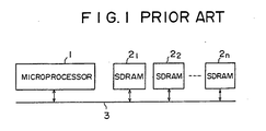
- Fig. 1 is a block diagram of a system having electronic systems in which a small-amplitude signal, which has an amplitude less than the power supply voltage, is transmitted therebetween via a bus line.
- the system shown in Fig. 1 includes a microprocessor 1, SDRAM (Synchronous Dynamic Random Access Memory) devices 2 1 , 2 2 and 2 n (where n is an integer), and a bus line 3 via which small-amplitude signals are transmitted.
- SDRAM Serial Dynamic Random Access Memory
- n is an integer
- the transmission of signals between the microprocessor 1 and the DRAM devices 2 1 - 2 n are carried out at tens of mega-hertz. However, it is required that signal transmissions be performed at 100 MHz or higher.
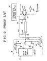
- Fig. 2 is a circuit diagram of conventional interfaces and a bus system employed in electronic systems as described above.
- a microprocessor 5 has a signal input/output terminal 6, a reference voltage input terminal 7 and an input circuit 8.
- the signal input/output terminal 6 is used to input and output a signal DQ.
- the reference voltage input terminal 7 is used to receive a reference voltage Vref.
- the input circuit 8 includes a differential amplifier circuit.
- the microprocessor 5 has a VCC power supply line 10 providing a power supply voltage VCC (equal to, for example, 3.3 V), a VSS power supply line via which a power supply voltage VSS (equal to, for example, 0 V), a main body circuit 11 and a push-pull-type output circuit 12.
- the push-pull-type output circuit 12 is made up of an enhancement-type p-channel MOS transistor 13 functioning as a pull-up element, and an enhancement-type n-channel MOS transistor 14 functioning as a pull-down element.
- a bus line 15 transmits small-amplitude signals.
- a termination voltage supply 16 generates a termination voltage VTT (equal to, for example, 1.65 V).
- a VTT voltage line 17 supplies the termination voltage VTT to parts connected thereto.
- Two termination resistors 18 and 19 (equal to, for example, 50 ⁇ ) are connected as shown in Fig. 2.
- An SDRAM device 20 has a signal input/output terminal 21 used to input and output the signal DQ, a reference voltage input terminal 22 receiving the reference voltage Vref, an input circuit 23 having a differential amplifier circuit, and a push-pull-type output circuit 24.
- the termination voltage VTT generated from the termination voltage supply 16 is applied, as the reference voltage Vref, to the reference voltage input terminal 7 of the microprocessor 5 and the reference voltage input terminal 22 of the SDRAM 20.
- Vref the reference voltage
- the pMOS transistor 13 is turned OFF (not conducting), and the nMOS transistor 14 is turned ON (conducting).
- the signal DQ is set to the low level (L).
- the pMOS transistor 13 is turned ON and the nMOS transistor 14 is OFF, the signal DQ is switched to the high level (H).
- the output circuit 12 outputs the low level, a current flows from the termination voltage supply 16 to the load.
- the output circuit 12 outputs the high level, a current flows the termination voltage supply 16 from the load.
- the termination voltage supply 16 is formed with a voltage source such as a switching regulator or a series regulator. However, such a regulator is not expected to receive current coming from the power supply. If a current comes into the voltage source from the load, the termination voltage VTT will be varied.
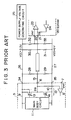
- the bus system shown in Fig. 3 includes a power supply voltage generating circuit 25 for generating the power supply voltage VCC.
- the circuit 25 is connected to a VCC power supply line 26. Further, there is provided a VSS power supply line 27. Further, the system includes termination resistors 28 - 31 (each equal to, for example, 100 ⁇ ), voltage dividing resistors 32 and 33, and power supply voltage input terminals 34 and 35 of the microprocessor 5.
- the resistors 32 and 33 divide the power supply voltage VCC to thereby generate the reference voltage Vref.
- the termination part made up of the termination resistors 28 and 29 is set approximately equal to 50 n, and the termination part made up of the termination resistors 30 and 31 is set approximately equal to 50 ⁇ .
- the bus system shown in Fig. 3 has the following disadvantages.
- the termination resistors 28 and 29 as well as the termination resistors 30 and 31 are respectively connected in series between the VCC line 26 and the VSS line 27. Hence, even when no signal is transmitted, currents flow in the termination resistors 28 - 31 and increase power consumption.
- the voltage dividing resistors 32 and 33 are designed to have large resistance values, the current flowing in the resistors 32 and 33 can be reduced.
- the reference voltage Vref will not be equal to the termination voltage VTT.
- the difference between the reference voltage Vref and the termination voltage VTT functions as a D.C. offset voltage of the input signal, which reduces the operation margin at the high-level or low-level side of the input signal.
- a more specific object of the present invention is to provide an electronic system in which the termination voltage is stabilized with reduced power consumption and a sufficient operation margin for input signals can be ensured by preventing an offset voltage from being produced.
- Fig. 4 is a circuit diagram of an electronic system.
- the electronic system shown in Fig. 4 includes a voltage generating circuit 37, which includes a voltage generating circuit 38 for generating a voltage V1, a voltage generating circuit 39 for generating a voltage V2, and voltage output terminals 40 and 41.
- the voltage generating circuits 38 and 39 are connected in series. The voltages V1 and V2 generated by the circuits 38 and 39 are applied to the voltage output terminals 40 and 41, respectively.
- a power supply line 42 carries a power supply voltage equal to V1 + V2 generated by the voltage generating circuit 37.
- a termination voltage line 43 carries a termination voltage VTT equal to the voltage V2 output by the voltage generating circuit 37.
- An integrated circuit 44 performs inputting and outputting of signals via a signal input/output terminal 45.
- the integrated circuit 44 has a power supply voltage input terminal 46, which receives the power supply voltage V1 + V2, and a power supply line 47 which supplies the voltage V1 + V2 as a power supply voltage.
- the integrated circuit 44 has a push-pull-type output circuit 48.
- the push-pull-type output circuit 48 includes a p-channel insulation gate type field effect transistor 49 functioning as a pull-up element, and an n-channel insulation gate type field effect transistor 50 functioning as a pull-down element.
- the system shown in Fig. 4 includes a bus line forming a signal transmission path, and a termination resistor 52 which terminates the bus line 51.
- the system includes an integrated circuit 53, which performs inputting and outputting of signals.
- the integrated circuit 53 has a signal input terminal 54 which inputs signals, a reference voltage input terminal 55 to which the voltage V2 output from the voltage generating circuit 37 is applied, and an input circuit 56.
- the output circuit 48 is supplied with the voltage V1 + V2 as the power supply voltage, and the termination resistor 52 is supplied with the voltage V2 as the termination voltage VTT.
- the termination voltage VTT can be set equal to half of the voltage V1 + V2.
- a current i Q flows, in the following order, in a closed circuit made up of the voltage generating circuit 39, the termination voltage line 43, the termination resistor 52, the bus line 51, the n-channel transistor 50, the ground, and the voltage generating circuit 39. - Hence, the voltage of the voltage output terminal 41 is maintained at the voltage V2.
- a current i 1 flows, in the following order, in a closed circuit made up of the voltage generating circuit 38, the power supply line 42, the transistor 49, the bus line 51, the termination resistor 52, and the voltage generating circuit 38. Hence, the voltage of the voltage output terminal 41 is maintained at the voltage V2.
- the voltage output terminal 41 can be maintained at the voltage V2 even when a current enters the voltage generating circuit 37, so that the stability in which the termination voltage VTT is equal to the voltage V2 can be ensured. Further, when the bus line 51 does not transmit any signal, no current flows in the termination resistor 52, whereby the power consumption can be reduced. Furthermore, the termination voltage VTT can be used as the reference voltage Vref with respect to the integrated circuits 44 and 53. Hence, it is possible to coincide the reference voltage Vref with the termination voltage VTT and prevent an occurrence of an offset voltage and to ensure a sufficient operation margin.
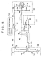
- Fig. 5 is a circuit diagram of an electronic system according to the present invention.
- the system includes a voltage generating circuit 58, which generates a voltage V3.
- a power supply line 59 for supplying the voltage V3 as the power supply voltage is connected to the circuit 58.
- the system includes a voltage generating circuit 60, which generates a voltage V4.
- the circuit 60 includes a power supply voltage input terminal 61 receiving the voltage V3, a power supply line 62 and an operational amplifier 63.
- the voltage generating circuit 60 includes voltage dividing resistors 64 and 65, which divide the voltage V3.
- the voltage generating circuit 60 includes a voltage output terminal 66 via which the voltage V4 is output, and a termination voltage line 67 for supplying the voltage V4 output from the voltage generating circuit 60 as the termination voltage VTT.
- the voltage V3 is divided by the resistors 64 and 65 to thereby generate a divided voltage applied to the first input terminal of the operational amplifier 63.
- the output of the operational amplifier 63 is fed back to the second input terminal thereof.
- the second input terminal that is, the voltage output terminal 66 is supplied with the same voltage V4 as the divided voltage divided by the resistors 64 and 66.
- the system includes an integrated circuit 68, which has a signal input/output terminal 69 via which signals are input and output, a power supply voltage input terminal 70 via which the voltage V3 is received as the power supply voltage, a power supply line 71 via which the voltage V3 is supplied as the power supply voltage, and a push-pull-type output circuit 72.
- the push-pull-type output circuit 72 includes a p-channel insulation gate type field effect transistor 73 functioning as a pull-up element, and an n-channel insulation gate type field effect transistor 74 functioning as a pull-down element.
- a bus line 75 serving as a signal transmission path, and a termination resistor 76 which terminates the bus line 75.
- the system further includes an integrated circuit 77 via which signals are input and output.
- the circuit 77 includes a signal input terminal 78 via which signals are input, a reference voltage input terminal 79 via which the voltage V4 output by the voltage generating circuit 60 is supplied as the reference voltage Vref, and an input circuit 80.
- the termination voltage VTT is written as V3 x R 65 /(R 64 + R 65 ), so that a small-amplitude signal having the center voltage equal to the termination voltage VTT can be transmitted.
- R 64 R 65
- the termination voltage VTT can be set equal to V3/2.
- a current i 3 flows, in the following order, in a closed circuit made up of the operational amplifier 63, the termination voltage line 67, the termination resistor 76, the bus line 75, the transistor 74, the ground, the voltage generating circuit 58, the power supply lines 59 and 62 and the operational amplifier 63.
- a current i 4 flows, in the following order, in a closed circuit made up of the voltage generating circuit 58, the power supply lines 59 and 71, the transistor 73, the bus line 75, the termination resistor 76, the termination voltage line 67, the operational amplifier 63, the ground and the voltage generating circuit 58.
- the system according to the present invention is configured so that the voltage V4 equal to the termination voltage VTT is fed back by means of the operational amplifier 63. Hence even when a current is output or input via the voltage output terminal 66, the stability in which the termination voltage VTT is equal to V4 can be ensured.
- the termination voltage VTT can be used as the reference voltage Vref for the integrated circuits 68 and 77, it is possible to coincide the reference voltage Vref with the termination voltage VTT and prevent an occurrence of an offset voltage and to ensure a sufficient operation margin.
- An electronic system shown in Fig. 6 includes a voltage generating circuit 83, which includes voltage generating circuits 84 and 85 and voltage output terminals 86 and 87.
- Each of the voltage generating circuits 84 and 85 generates a voltage V5 equal to, for example, 1.0 V.
- the voltage generating circuits 84 and 85 are connected in series.
- the electronic system includes a microprocessor 90 and SDRAM devices 91 - 94, each of which devices performs an input/output operation on data of eight bits DQ0 - DQ7.
- Reference numbers 95 - 99 indicate data input/output terminals via which data is input and output.
- Reference numbers 100 - 104 indicate reference voltage input terminals via which the reference voltage Vref is received.
- the termination voltage VTT is supplied, as the reference voltage Vref, to the microprocessor 90 and the SDRAM devices 91 - 94.
- the microprocessor 90 includes an input circuit 105 and a push-pull-type output circuit 110, which circuits handle data DQ0.
- the SDRAM devices 91 - 94 include input circuits 106 - 109 and push-pull-type output circuits 111 - 114, these input and output circuits handling data DQ0.
- a bus line 115 is provided for transmitting data DQ0.
- Termination resistors 116 and 117 are connected to the two ends of the bus line 115.
- the termination resistor 116 has a resistance of 50 ⁇
- the termination resistor 117 has a resistance of 30 n.
- the input and output circuits of the microprocessor 90 and the SDRAM devices 91 - 94 have an identical circuit configuration, and only the input and output circuit of the microprocessor 90, which is a part thereof, is illustrated in Fig. 7.
- the microprocessor 90 has a VCC power supply terminal 119 to which the power supply voltage VCC (for example, 3.3 V) is applied, a VCCQ power supply terminal 120 to which the power supply voltage VCCQ (2.0V, for example) is applied, and a VSS power supply terminal 121 to which the ground voltage VSS (OV) is applied.
- the microprocessor 90 has a VCC power supply line 122 connected to the VCC power supply terminal 119, a VCCQ power supply line 123 connected to the VCCQ power supply terminal 120, and a VSS power supply line 124 connected to the VSS power supply terminal 121.
- the microprocessor 90 has a main body circuit 125 to which the power supply voltage VCC is applied.
- the symbol /DATA (“/" is equivalent to the symbol “bar” in Fig. 7) denotes data output from the main body circuit 125, and the symbol /HZ denotes a control signal determining whether the output state should be set to a high-impedance state.
- An output control circuit 126 is supplied with the power supply voltage VCC, and is made up of a NOR circuit 127, an inverter 128 and a NAND circuit 129.
- An output driving circuit (pre-driver) 130 is supplied with the power supply voltage VCCQ, and is made up of enhancement-type p-channel MOS transistors 133 and 134, and enhancement-type n-channel MOS transistors 135 and 136.
- the output circuit 110 is made up of an enhancement-type pMOS transistor 137 serving as a pull-up element, and an enhancement-type nMOS transistor 138 serving as a pull-down element.
- the above current may damage the pMOS transistors 133, 134 and 137.
- the power supply voltage VCCQ is applied as the back bias voltage to the N-type well in which the pMOS transistors 133, 134 and 137 are formed. Even when the power supply voltages VCC and VCCQ become 0 V and 2 V, respectively, at the time of power on or off, the current is prevented from flowing from the sources of the pMOS transistors 133, 134 and 137 to the N-type well in which the pMOS transistors 133, 134 and 137 are formed. As a result, it is possible to prevent the pMOS transistors 133, 134 and 137 from being damaged.
- the output level of the inverter 128 is high and the output level of the NOR circuit 127 is low.
- the pMOS transistor 133 is ON and the nMOS transistor 135 is OFF.
- the output level of an inverter 131 is high, and thus the pMOS transistor 137 is OFF.
- the output level of the NAND circuit 129 is high, and the pMOS transistor 134 is OFF.
- the nMOS transistor 136 is ON, and the output level of an inverter 132 is low.
- the nMOS transistor 138 is OFF.
- the output circuit 110 is in the high-impedance state (Hi-Z).
- the output level of the NOR circuit 127 is low.
- the pMOS transistor 133 is ON and the nMOS transistor 135 is OFF.
- the output level of the inverter 131 is high, and the pMOS transistor 137 is OFF.
- the output level of the NAND circuit 129 is low, and the pMOS transistor 134 is ON.
- the nMOS transistor 136 is OFF, and the output level of the inverter 132 is high.
- the nMOS transistor 138 is ON.
- the signal DQ0 output from the output circuit 110 is low.
- the output level of the NOR circuit 127 is high.
- the pMOS transistor 133 is OFF, and the nMOS transistor 135 is ON.
- the output level of the inverter 131 is low, and the pMOS transistor 137 is ON.
- the output level of the NAND circuit 129 is high, and the pMOS transistor 134 is OFF.
- the nMOS transistor 136 is ON, and the output level of the inverter 132 is low.
- the nMOS transistor 138 is OFF.
- the signal DQ0 output from the output circuit 110 is high.
- the SDRAM devices 91 - 94 are connected to the bus line 115 at equal intervals, and there is provided only the bus line 115 between the microprocessor 90 and the DRAM device 91.
- the characteristic impedance of the bus line 115 is denoted as Z0
- the effective characteristic impedance of parts of the bus line 115 via which the SDRAM devices 91 - 94 are connected at equal intervals are less than that of parts thereof to which the SDRAM devices 91 - 94 are not connected.
- L 250 nH/m
- C 100 pF.
- the resistance values of the termination resistors 116 and 117 should be set equal to the effective characteristic impedance ZL, that is, 18.9 ⁇ .
- the load resistance viewed from the driving side is 9.45 ⁇ .
- the input circuits 105 - 109 cannot operate stably and provide the sufficient amplitude unless the output circuits 110 - 114 have a current driving ability of approximately 20 mA.
- the value of the termination resistor 117 around which the SDRAM devices 91 - 94 are concentrated is omitted from the strict matching condition, and is made greater than the effective characteristic impedance ZL.
- the above value is limited to the characteristic impedance Z0 of the bus line 115 with no load connected thereto, more specifically, 30 ⁇ .
- the value of the termination resistor 116 is set equal to 50 ⁇ , which is equal to the characteristic impedance of the bus line 115 obtained when there is no load.
- the load resistance viewed from the driving side is 18.7 ⁇ , which is equal to the parallel-connection value of 30 ⁇ and 50 ⁇ .
- the load resistance is greater than that obtained when a resistance of 30 ⁇ is simply connected on either side of the bus line 115 (the load resistance then being equal to 15 n).
- the output circuits 110 - 114 of the microprocessor 90 and the SDRAM devices 91 - 94 are formed with the CMOS-type push-pull circuits to which the power supply voltage VCCQ is applied. Further, the termination voltage VTT is equal to VCCQ/2, and thus the signals can be transmitted in such a way that the center voltage is equal to the termination voltage VTT.
- a current flows in a closed circuit made up of the voltage generating circuit 85, the termination voltage line 89, the termination resistors 116 and 117, the bus line 115, the output circuit 110 (nMOS transistor 138), the ground and the voltage generating circuit 85 in the above order.
- a current flows in a closed circuit made up of the voltage generating circuit 84, the VCCQ power supply line 88, the output circuit 110 (pMOS transistor 137), the bus line 115, the termination resistors 116 and 117 and the voltage generating circuit 84 in the above order.
- the voltage generating circuits 84 and 85 of the voltage generating circuit 83 are connected in series, the voltage of the voltage output terminal 87 is maintained at V5 equal to 1.0 V even if a current is output or input via the voltage output terminal 87. Hence, it is possible to ensure the stability that the termination voltage VTT is equal to the voltage V5 equal to 1.0 V.
- the termination voltage VTT is used as the reference voltage Vref which is needed in the microprocessor 90 and the SDRAM devices 91 - 94. Hence, the coincidence of the reference voltage Vref and the termination voltage VTT can be accomplished and no offset voltage is generated. Hence, a sufficient operation margin can be ensured.
- the power supply voltage VCCQ is supplied as the power supply voltage necessary for the output driving circuit 130 to drive the output circuits 110 - 114. Hence, it is possible to drive the pMOS transistor serving as the pull-up element and the nMOS transistor serving as the pull-down element in a balanced way.
- the output control circuit 126, the output driving circuit 130 and the output circuit 110 in the microprocessor 90 can be configured as shown in Fig. 11.
- the circuit shown in Fig. 11 can be applied to the SDRAM devices 91 - 94 as well.
- the output control circuit 126 is made up of a NAND circuit 141, an inverter 142 and a NOR circuit 143.
- the output driving circuit 130 is a CMOS type inverter to which the power supply voltage VCC is applied.
- the CMOS inverter is made up of an enhancement type pMOS transistor 145 and an enhancement type nMOS transistor 146.
- the output circuit 110 is made up of a depletion type nMOS transistor 147 functioning as a pull-up element and an enhancement type nMOS transistor 148 functioning as a pull-down element.
- the output circuit 110 is intended to improve the driving ability of the pull-up element.
- the threshold voltage V THD of the nMOS transistor 147 is set to -V 0L ⁇ V THD .
- the threshold voltage V THD is equal to or greater than -0.75V.
- the output level of the inverter 142 is low, and the output level of the NAND circuit 141 is high.
- the pMOS transistor 145 is OFF, and the nMOS transistor 146 is ON.
- the output level of the inverter 144 is low, and the nMOS transistor 147 is OFF.
- the output level of the NOR circuit 143 is low, and the nMOS transistor 148 is OFF. In this case, the output circuit 110 is in the high-impedance state.
- the nMOS transistor 147 may be replaced by an enhancement-type nMOS transistor.
- the threshold voltage of the enhancement type nMOS transistor is lower than the threshold voltage of the nMOS transistor 148, the advantage of an increase in the driving ability may be canceled by a decrease in the threshold voltage.
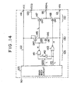
- Fig. 15 is a circuit diagram of the essential part of an electronic system.
- the electronic system shown in Fig. 15 has a voltage generating circuit 150, which generates voltages different from those generated by the voltage generating circuit 83 shown in Fig. 6.
- the voltage generating circuit 150 has voltage generating circuits 151 and 152, each generating a voltage V6 (1.65 V, for example), and voltage output terminals 153 and 154. More specifically, the voltage generating circuits 151 and 152 are connected in series.
- the bus line 115 shown in Fig. 15 has branched parts 155 - 159, that is, stubs. Resistors 160 - 164 are connected between branch points on the bus line 115 and the stubs 155 - 159.
- the power supply voltage VCCQ supplied via the VCCQ power supply line 88 is supplied to the VCC power supply terminals and the VCCQ power supply terminals of the microprocessor 90 and the SDRAM devices 91 - 94.
- the VCC power supply terminals of the microprocessor 90 and the SDRAM devices 91 - 94 are connected to the VCCQ power supply terminals outside thereof.
- Fig. 16 shows such a connection for the microprocessor 90.
- nain body circuit 125 and the output control circuit 126 are driven by the power supply voltage VCCQ equal to 3.3 V.
- the gate of the nMOS transistor 138 is also supplied with the power supply voltage VCCQ of 3.3 V, so that the inner resistance of the nMOS transistor 138 is decreased and an excessive current flows in the output.
- the resistor 160 is connected between the branching point on the bus line 115 and the stub 155 in order to select an appropriate inner resistance value of the output circuit 110 and prevent changes in the driving currents with respect to the termination resistors 116 and 117.
- the resistors 161 - 164 are connected between the branch points on the bus line 115 and the stubs 156 - 159.
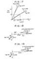
- Figs. 17 and 18 show how to determine the resistance values of the resistors 160 - 164. More particularly, Fig. 17 is a graph of the static characteristic of the nMOS transistor 138 in the output circuit 110 of the microprocessor 90, and Fig. 18 shows part of the configuration shown in Fig. 15. In the second embodiment of the present invention, the nMOS transistor 138 is configured so as to have a static characteristic as shown in Fig. 17. In the case where the nMOS transistor 138 is turned ON with the VCCQ equal to 3.3 V, the gate-source voltage V GS thereof is equal to 3.3 V, while the drain-source voltage V DS thereof is equal to 0.2 V.
- the load resistance value is equal to 25 ⁇
- the voltage drops developing across the termination resistors 116 and 117 are equal to 0.25 V, as shown in Fig. 18.
- the resistance values of the resistors 161 - 164 are selected in the same way as the resistor 160.
- the characteristic impedances of the stubs 155 - 159 can be determined as follows. First of all, the resistance values of the resistors 160 - 164 are set equal to 120 ⁇ taking into consideration the driving ability of the output circuit. Since the characteristic impedance of the bus line 115 is 50 ⁇ , two resistors having resistances of 50 n connected in parallel are seen when viewing the bus line 115 from the branch node. That is, a characteristic impedance of 25 n can be seen as a load.
- the resistors 160 - 164 respectively have a resistance of 120 n
- the characteristic impedances of the stubs 155 - 159 are appropriately set equal to 145 ⁇ . It has been confirmed through a simulation that the above value causes no problems even when it varies within the range of ⁇ 50 %.
- the signal is input to the stubs 155 - 159 from the bus line 115, the input/output terminals 95 - 99 have no terminations.
- the input signal is totally reflected (100% reflection).
- reflection does not take place when the reflected signal is transmitted to the resistors 160 - 164 because the impedance match is established. That is, the signal is absorbed by the termination resistors 116 and 117 after it comes in the bus 115. Hence, thereafter, the resonance phenomenon does not occur after the stubs 155 - 159, and good signal transmissions can be carried out.
- the gate-source voltage V GS is equal to 2.0 V
- the drain-source voltage V DS is equal to 0.75 V.
- the driving current for the nMOS transistor 138 is equal to 10 mA
- the resistances of the termination resistors 116 and 117 are equal to 50 ⁇
- the load resistance is 25 ⁇
- the voltage drops developing across the termination resistors 116 and 117 become equal to 0.25 V as shown in Fig. 19.
- the resistor 160 is not needed. That is, when decreasing the power supply voltage VCCQ, the resistors 160 - 164 are needed no longer, and the number of parts can be reduced.
- the resonances caused in the stubs 155 - 159 cannot be suppressed by means of impedance matching. Hence, it is necessary to reduce the lengths of the stubs 155 - 159 as much as possible.
- the output circuits 110 - 114 of the microprocessor 90 and the SDRAM devices 91 - 94 are formed by the CMOS type push-pull circuits supplied with the power supply voltage VCCQ. Further, the termination voltage VTT is set to VCCQ/2. Hence, it is possible to transmit small-amplitude signals having the center voltage equal to the termination voltage VTT.
- a current flows, in the following order, in a closed circuit made up of the voltage generating circuit 152, the termination voltage line 89, the termination resistors 116 and 117, the bus line 115, the output circuit 110 (nMOS transistor 138), the ground and the voltage generating circuit 152.
- a current flows in a closed circuit made up of the voltage generating circuit 151, the VCCQ power supply line 88, the output circuit 110 (pMOS transistor 137), the bus line 115, the termination resistors 116 and 117, and the voltage generating circuit 151.
- the termination voltage VTT is used as the reference voltage Vref which is needed in the microprocessor 90 and the SDRAM devices 91 - 94. Hence, the coincidence of the reference voltage Vref and the termination voltage VTT can be accomplished and no offset voltage is generated. Hence, the sufficient operation margin can be ensured.
- the resistors 160 - 164 are provided at the branch points on the bus line 115. Hence, it is possible to not only prevent an excessive current from flowing in the circuits but also to cut off, by means of the resistors 160 - 164, highfrequency components contained in the reflected signals produced at the stubs 155 - 159 in the case where these stubs are needed. As a result, it is difficult for the transmitted signal waveforms to be deformed. From these viewpoints, it can be said that the second embodiment of the present invention is suitable for a system in which the SDRAM devices 91 - 94 are mounted on a module (SIMM) and connectors of the module are connected to the bus line 115. Meanwhile, the structure is suitable for a system in which the SDRAM devices 91 - 95 are directly connected to the bus line 115 because it does not need the stubs 155 - 159.
- SIMM module
- Fig. 19A is a circuit diagram of a practical example of the voltage generating circuit 150 shown in Fig. 15.
- the circuit shown in Fig. 19A is a switching regulator.
- the voltage generating circuit 150 shown in Fig. 19A includes a pMOS transistor Q1, an nMOS transistor Q2, diodes D1 and D2, an inductor L, capacitors C1 and C2, and a control circuit 150A.
- the control circuit 150A includes a comparator COMP and a driver DRV having two CMOS inverters.
- the transistors Q1 and Q2 function as switches of the switching regulator.
- the diodes D1 and D2 allow a counter electromotive force of the inductance to pass therethrough.
- the inductor L and the capacitors C1 and C2 form a smoothing circuit.
- the comparator output turns ON and OFF the transistors Q1 and Q2 with the equal duty ratio. In this state, the circuit is in the oscillating state.
- the control circuit 150A can be formed by Si9145 manufactured by Siliconics in the United States.
- the voltage generating circuit 83 shown in Fig. 6 can be configured in the same way as described above.
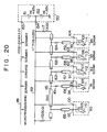
- Fig. 20 is a circuit diagram of the essential part of an electronic system.
- the resistors 161 - 164 are connected between the bus line 115 and the stubs 156 - 159, while no resistor is intentionally connected between the microprocessor 90 and the bus line 115.
- the microprocessor 90 is mounted on PGA (Pin Grid Array) packages and has a large number of pins. Hence, many cases will take place in which no space for providing the resistor 160 shown in Fig. 15 is available.
- the resistors 161 - 164 are connected between the bus line 115 and the stubs 156 - 159, while the resistor 160 shown in Fig. 15 is not provided between the bus line 115 and the processor 90. Even when the resistor 160 is not used, the microprocessor 90 would be connected to an end portion of the bus line 115 in many cases. This end portion is close to the termination resistor 116, which functions to reduce deformation in the signal waveforms.
- the output circuit 110 of the microprocessor 90 is designed to have a small driving ability and the inner resistance thereof is as high as approximately 100 ⁇ .
- the decreasing of the inner resistance of the output circuit 110 to approximately 100 ⁇ can be achieved by adjusting the sizes of the pMOS transistor 137 and the nMOS transistor 138, or providing a resistor in series to the output of the output circuit 110 at a position close to the output circuit 110, for example, on the chip or in the package.
- the gate width of the pMOS transistor 137 is set to, for example, 500 ⁇ m and the gate length thereof is set to, for example, 1 ⁇ m. Further, the gate width of the nMOS transistor 138 is set to, for example, 200 ⁇ m, and the gate length thereof is set to, for example, 1 ⁇ m.
- the gate width and gate length of the pMOS transistor 137 are set to, for example, 1000 ⁇ m and 1 ⁇ m, respectively. Further, the gate width and gate length of the nMOS transistor 138 are set to, for example, 400 ⁇ m and 1 ⁇ m, respectively.
- the resistor connected in series to the output circuit 110 has a negative temperature coefficient, it advantageously functions to cancel a positive temperature coefficient of the inner resistances of the transistors of the output circuit 110.
- the series-connected resistor of an amorphous-system semiconductor material generally called thermistor.
- the series-connected resistor is formed by a diffused layer formed in a semiconductor substrate.
- the p-type diffused layer has a temperature coefficient greater than that of the n-type diffused layer.
- Such diffused layers are suitable for the above purpose.
- the above-mentioned materials have natures in which the resistance is decreased as the temperature increases. Hence, it is possible to cancel a phenomenon such that the driving abilities of transistors are decreased as the temperature increases.
- Fig. 21 is a circuit diagram of the essential part of an electronic system.
- a temperature sensor 165 is provided to control the voltage V6 generated by the voltage generating circuits 151 and 152 on the basis of the temperature sensed by the temperature sensor.
- the resistors 161 - 164 are connected between the bus line 115 and the stubs 156 - 159, and no resistor is connected to the bus line 115 and the microprocessor 90.
- the transistors in the output circuit 110 of the microprocessor 90 have small driving abilities. It should be noted that the MOS transistors have negative driving current temperature coefficients, in which the driving ability is degraded as the operation temperature increases.
- the voltage V6 output from the voltage generating circuits 151 and 152 have a positive temperature coefficient.
- the appropriate value of the voltage V6 is 1.3 V at 25°C and 1.65 V at 100 °C.
- Fig. 22 is a circuit diagram of the essential part of the electronic system according to the embodiment of the present invention.
- the voltage generating circuit 83 shown in Fig. 6 is replaced by a termination voltage generating circuit 166.
- a VCCQ power supply line 167 for supplying the power supply voltage VCCQ equal to 2.0 V to the termination voltage generating circuit 166
- a VSSQ power supply line 168 for supplying the power.
- supply voltage VSSQ equal to 0 V to the termination voltage generating circuit 166.
- the power supply voltage VCCQ from the VCCQ power supply line 167 is supplied to the microprocessor 90 and the SDRAM devices 91 - 94.
- the other parts of the circuit of the embodiment of the present invention are the same as those shown in Fig. 6.
- the termination voltage generating circuit 166 includes an operational amplifier 171, and voltage dividing resistors 172 and 173 having an identical resistance.
- the output of the operational amplifier 171 is fed back to the reverse phase (inverting) input terminal of the operational amplifier 171.
- the termination voltage VTT equal to VCCQ/2 is obtained at the output terminal of the operational amplifier 171.
- termination voltage generating circuit 166 There are integrally provided on one chip the termination voltage generating circuit 166, the voltage dividing resistors 172 and 173, the termination resistor 117 for the bus line 115 provided for the data DQ0, and termination resistors for the bus lines for data DQ1 - DQ7. These elements provided on one chip are packaged, as a termination module (termination device), with the same dimensions as the SDRAM devices 91 - 94.
- Fig. 23 schematically shows the termination module 174, which includes a termination module main body 175, termination resistors 176 - 181 respectively provided for data DQ1 - DQ7 and external terminals 182 - 200. These external terminals 182 - 200 are located in the same positions of the corresponding external terminals of each of the SDRAM device 91 - 94.
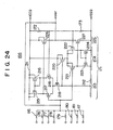
- Fig. 24 is a circuit diagram of the termination voltage generating circuit 166 used in the embodiment of the present invention.
- the circuit 166 includes a VCCQ power supply line 211, a VSSQ power supply line 212, and differential amplifier circuits 213 and 214.
- the differential amplifier circuit 213 includes enhancement type pMOS transistors 215 and 216 forming a current-mirror circuit functioning as a load.
- the circuit 166 includes enhancement type nMOS transistors 217 and 218 functioning as driving transistors, and an enhancement type nMOS transistor 219 functioning as a resistor.
- the differential amplifier circuit 214 includes an enhancement type pMOS transistor 220 functioning as a resistor, enhancement type pMOS transistors 221 and 222 functioning as driving transistors, and nMOS transistors 223 and 224 functioning as loads. Further, the termination voltage generating circuit 166 shown in Fig. 24 includes an output circuit 225, which is made up of an enhancement type pMOS transistor 226 functioning as a pull-up element, and an enhancement type nMOS transistor 227 functioning as a pull-down element.
Landscapes
- Engineering & Computer Science (AREA)
- Computer Hardware Design (AREA)
- Power Engineering (AREA)
- Computer Networks & Wireless Communication (AREA)
- Signal Processing (AREA)
- Physics & Mathematics (AREA)
- Computing Systems (AREA)
- General Engineering & Computer Science (AREA)
- Mathematical Physics (AREA)
- Microelectronics & Electronic Packaging (AREA)
- Logic Circuits (AREA)
- Dram (AREA)
Description
- The present invention generally relates to electronic systems which transmit signals to remote devices via signal lines, and more particularly to an electronic system which transmits a signal having an amplitude less than the power supply voltage applied to the electronic system.
- Recently, there has been considerable activity in the development of small-amplitude high-speed signal transmissions. In such transmissions, signals having amplitudes less than the power supply voltage are transmitted. For example, the GTL (Gunning Transceiver Logic) standard is known. According to this GTL standard, the output circuit is an open-drain type driver and an impedance match termination is employed. Under these conditions, the following parameters are defined:


- Regarding the small-amplitude high-speed signal transmissions, the following documents are known: 1) Taguchi et al., "COMPARING SMALL-AMPLITUDE INTERFACES TOWARD 100 MHZ TIMES", Nikkei Electronics, No. 591, pp. 269 - 290, 1993. 9. 27; and 2) Taguchi et al., "SMALL-AMPLITUDE INTERFACE CIRCUIT FOR HIGH-SPEED MEMORY BUS", Study Document of Institute of Electronics, Communication and Information Engineers, November 26, 1993.
- Fig. 1 is a block diagram of a system having electronic systems in which a small-amplitude signal, which has an amplitude less than the power supply voltage, is transmitted therebetween via a bus line. The system shown in Fig. 1 includes a
microprocessor 1, SDRAM (Synchronous Dynamic Random Access Memory)devices bus line 3 via which small-amplitude signals are transmitted. At the present time, the transmission of signals between themicroprocessor 1 and the DRAM devices 21 - 2n are carried out at tens of mega-hertz. However, it is required that signal transmissions be performed at 100 MHz or higher. - Fig. 2 is a circuit diagram of conventional interfaces and a bus system employed in electronic systems as described above. A microprocessor 5 has a signal input/
output terminal 6, a referencevoltage input terminal 7 and aninput circuit 8. The signal input/output terminal 6 is used to input and output a signal DQ. The referencevoltage input terminal 7 is used to receive a reference voltage Vref. Theinput circuit 8 includes a differential amplifier circuit. Further, the microprocessor 5 has a VCCpower supply line 10 providing a power supply voltage VCC (equal to, for example, 3.3 V), a VSS power supply line via which a power supply voltage VSS (equal to, for example, 0 V), a main body circuit 11 and a push-pull-type output circuit 12. - The push-pull-
type output circuit 12 is made up of an enhancement-type p-channel MOS transistor 13 functioning as a pull-up element, and an enhancement-type n-channel MOS transistor 14 functioning as a pull-down element. - A
bus line 15 transmits small-amplitude signals. Atermination voltage supply 16 generates a termination voltage VTT (equal to, for example, 1.65 V). AVTT voltage line 17 supplies the termination voltage VTT to parts connected thereto. Twotermination resistors 18 and 19 (equal to, for example, 50 Ω) are connected as shown in Fig. 2. AnSDRAM device 20 has a signal input/output terminal 21 used to input and output the signal DQ, a referencevoltage input terminal 22 receiving the reference voltage Vref, aninput circuit 23 having a differential amplifier circuit, and a push-pull-type output circuit 24. - In the configuration shown in Fig. 2, the termination voltage VTT generated from the
termination voltage supply 16 is applied, as the reference voltage Vref, to the referencevoltage input terminal 7 of the microprocessor 5 and the referencevoltage input terminal 22 of theSDRAM 20. - In the interface circuits and the bus system shown in Fig. 2, the signal DQ is transmitted in such a way that a center voltage is set equal to the reference voltage Vref (= 1.65 V), and the amplitude is within the range of ±400 mV. For example, when the microprocessor 5 sends the signal DQ to the
DRAM device 20, thepMOS transistor 13 is turned OFF (not conducting), and thenMOS transistor 14 is turned ON (conducting). In this case, the signal DQ is set to the low level (L). When thepMOS transistor 13 is turned ON and thenMOS transistor 14 is OFF, the signal DQ is switched to the high level (H). When theoutput circuit 12 outputs the low level, a current flows from thetermination voltage supply 16 to the load. When theoutput circuit 12 outputs the high level, a current flows thetermination voltage supply 16 from the load. - Generally, the
termination voltage supply 16 is formed with a voltage source such as a switching regulator or a series regulator. However, such a regulator is not expected to receive current coming from the power supply. If a current comes into the voltage source from the load, the termination voltage VTT will be varied. - Taking into account the above, a bus system as shown in Fig. 3 can be used. The bus system shown in Fig. 3 includes a power supply
voltage generating circuit 25 for generating the power supply voltage VCC. Thecircuit 25 is connected to a VCCpower supply line 26. Further, there is provided a VSSpower supply line 27. Further, the system includes termination resistors 28 - 31 (each equal to, for example, 100 Ω),voltage dividing resistors voltage input terminals resistors - In the bus system, the termination part made up of the
termination resistors termination resistors - However, the bus system shown in Fig. 3 has the following disadvantages. The
termination resistors termination resistors VCC line 26 and theVSS line 27. Hence, even when no signal is transmitted, currents flow in the termination resistors 28 - 31 and increase power consumption. - If the
voltage dividing resistors resistors resistors precision resistors - An electronic system with the features of the upper clause of
claim 1 is known from DE-A-41 42 081. - It is a general object of the present invention to provide an electronic system in which the above disadvantages are eliminated.
- A more specific object of the present invention is to provide an electronic system in which the termination voltage is stabilized with reduced power consumption and a sufficient operation margin for input signals can be ensured by preventing an offset voltage from being produced.
- These objects of the present invention are achieved by the features of
claim 1. - The present invention is mainly disclosed in the description in connection with Figs. 5, 22, 23 and 24. The description of the other embodiments and examples is helpful in understanding the present invention.
- The scope of the present invention is defined by the only claim.
- Other aspects and advantages of the present invention will become more apparent from the following detailed description when read in conjunction with the accompanying drawings, in which:
- Fig. 1 is a block diagram of an electronic system in which a small-amplitude signal is transmitted;
- Fig. 2 is a circuit diagram of an interface circuit and a bus system applicable to the electronic device shown in Fig. 1;
- Fig. 3 is a circuit diagram of another interface circuit and another bus system applicable to the electronic device shown in Fig. 1;
- Fig. 4 is a circuit diagram of an electronic system not being part of the present invention;
- Fig. 5 is a circuit diagram of an electronic system according to the present invention;
- Fig. 6 is a circuit diagram of an example not being part of the present invention;
- Fig. 7 is a circuit diagram of part of a microprocessor shown in Fig. 6;
- Figs. 8, 9 and 10 are circuit diagrams showing the operation of the circuit shown in Fig. 7;
- Fig. 11 is a circuit diagram of another example of part of the microprocessor shown in Fig. 6;
- Figs. 12, 13 and 14 are circuit diagrams of the circuit shown in Fig. 11;
- Fig. 15 is a circuit diagram of an example not being part of the present invention;
- Fig. 16 is a circuit diagram of part of a microprocessor shown in Fig. 15;
- Fig. 17 is a graph of the static characteristic of an nMOS transistor shown in Fig. 16;
- Fig. 18 is a circuit diagram of part of the example of Fig. 15;
- Fig. 19 is a circuit diagram of part of the example of Fig. 6;
- Fig. 19A is a circuit diagram of a voltage generating circuit;
- Fig. 20 is a circuit diagram of another example;
- Fig. 21 is a circuit diagram of another example;
- Fig. 22 is a circuit diagram of an essential part of an embodiment of the present invention;
- Fig. 23 is a circuit diagram of a termination module shown in Fig. 22.
- Fig. 24 is a circuit diagram of a termination voltage generating circuit used in the embodiment of the present invention;
- Fig. 4 is a circuit diagram of an electronic system.
- The electronic system shown in Fig. 4 includes a
voltage generating circuit 37, which includes avoltage generating circuit 38 for generating a voltage V1, avoltage generating circuit 39 for generating a voltage V2, andvoltage output terminals voltage generating circuits circuits voltage output terminals - A
power supply line 42 carries a power supply voltage equal to V1 + V2 generated by thevoltage generating circuit 37. Atermination voltage line 43 carries a termination voltage VTT equal to the voltage V2 output by thevoltage generating circuit 37. Anintegrated circuit 44 performs inputting and outputting of signals via a signal input/output terminal 45. Theintegrated circuit 44 has a power supplyvoltage input terminal 46, which receives the power supply voltage V1 + V2, and apower supply line 47 which supplies the voltage V1 + V2 as a power supply voltage. Further, theintegrated circuit 44 has a push-pull-type output circuit 48. The push-pull-type output circuit 48 includes a p-channel insulation gate typefield effect transistor 49 functioning as a pull-up element, and an n-channel insulation gate typefield effect transistor 50 functioning as a pull-down element. - Further, the system shown in Fig. 4 includes a bus line forming a signal transmission path, and a
termination resistor 52 which terminates thebus line 51. The system includes anintegrated circuit 53, which performs inputting and outputting of signals. Theintegrated circuit 53 has asignal input terminal 54 which inputs signals, a referencevoltage input terminal 55 to which the voltage V2 output from thevoltage generating circuit 37 is applied, and aninput circuit 56. - In the system shown in Fig. 4, the
output circuit 48 is supplied with the voltage V1 + V2 as the power supply voltage, and thetermination resistor 52 is supplied with the voltage V2 as the termination voltage VTT. Hence, it is possible to transmit a signal having a center voltage equal to V2. When the voltages V1 and V2 are set equal to each other, the termination voltage VTT can be set equal to half of the voltage V1 + V2. - When the
transistor 49 is turned OFF and thetransistor 50 is turned ON, the output of theoutput circuit 48 is switched to the low level. In this case, a current iQ flows, in the following order, in a closed circuit made up of thevoltage generating circuit 39, thetermination voltage line 43, thetermination resistor 52, thebus line 51, the n-channel transistor 50, the ground, and thevoltage generating circuit 39. - Hence, the voltage of thevoltage output terminal 41 is maintained at the voltage V2. - When the
transistor 49 is turned ON and thetransistor 50 is turned OFF, the output of the output circuit is switched to the high level. In this case, a current i1 flows, in the following order, in a closed circuit made up of thevoltage generating circuit 38, thepower supply line 42, thetransistor 49, thebus line 51, thetermination resistor 52, and thevoltage generating circuit 38. Hence, the voltage of thevoltage output terminal 41 is maintained at the voltage V2. - In the way as described above, , since the
voltage generating circuit 37 is made up of thevoltage generating circuits voltage output terminal 41 can be maintained at the voltage V2 even when a current enters thevoltage generating circuit 37, so that the stability in which the termination voltage VTT is equal to the voltage V2 can be ensured. Further, when thebus line 51 does not transmit any signal, no current flows in thetermination resistor 52, whereby the power consumption can be reduced. Furthermore, the termination voltage VTT can be used as the reference voltage Vref with respect to theintegrated circuits - Fig. 5 is a circuit diagram of an electronic system according to the present invention. The system includes a
voltage generating circuit 58, which generates a voltage V3. Apower supply line 59 for supplying the voltage V3 as the power supply voltage is connected to thecircuit 58. The system includes avoltage generating circuit 60, which generates a voltage V4. Thecircuit 60 includes a power supplyvoltage input terminal 61 receiving the voltage V3, apower supply line 62 and an operational amplifier 63. Further, thevoltage generating circuit 60 includesvoltage dividing resistors voltage generating circuit 60 includes avoltage output terminal 66 via which the voltage V4 is output, and atermination voltage line 67 for supplying the voltage V4 output from thevoltage generating circuit 60 as the termination voltage VTT. - In the
voltage generating circuit 60, the voltage V3 is divided by theresistors voltage output terminal 66 is supplied with the same voltage V4 as the divided voltage divided by theresistors - The system includes an
integrated circuit 68, which has a signal input/output terminal 69 via which signals are input and output, a power supplyvoltage input terminal 70 via which the voltage V3 is received as the power supply voltage, apower supply line 71 via which the voltage V3 is supplied as the power supply voltage, and a push-pull-type output circuit 72. The push-pull-type output circuit 72 includes a p-channel insulation gate typefield effect transistor 73 functioning as a pull-up element, and an n-channel insulation gate typefield effect transistor 74 functioning as a pull-down element. - Further, there are provided a
bus line 75 serving as a signal transmission path, and atermination resistor 76 which terminates thebus line 75. The system further includes anintegrated circuit 77 via which signals are input and output. Thecircuit 77 includes asignal input terminal 78 via which signals are input, a referencevoltage input terminal 79 via which the voltage V4 output by thevoltage generating circuit 60 is supplied as the reference voltage Vref, and aninput circuit 80. - Assuming that the resistance values of the
resistors - When the
transistor 73 is turned OFF and thetransistor 74 is turned ON, the output of theoutput circuit 72 is switched to the low level. In this case, a current i3 flows, in the following order, in a closed circuit made up of the operational amplifier 63, thetermination voltage line 67, thetermination resistor 76, thebus line 75, thetransistor 74, the ground, thevoltage generating circuit 58, thepower supply lines - When the
transistor 73 is turned ON and thetransistor 74 is OFF, the output of theoutput circuit 72 is switched to the high level. In this case, a current i4 flows, in the following order, in a closed circuit made up of thevoltage generating circuit 58, thepower supply lines transistor 73, thebus line 75, thetermination resistor 76, thetermination voltage line 67, the operational amplifier 63, the ground and thevoltage generating circuit 58. - As described above, the system according to the present invention is configured so that the voltage V4 equal to the termination voltage VTT is fed back by means of the operational amplifier 63. Hence even when a current is output or input via the
voltage output terminal 66, the stability in which the termination voltage VTT is equal to V4 can be ensured. - Further, when no signal is transmitted via the
bus line 75, no current flows in thetermination resistor 76, so that the power consumption can be reduced. Furthermore, since the termination voltage VTT can be used as the reference voltage Vref for theintegrated circuits - A description will now be given with reference to Fig. 6 through Fig. 24.
- First of all, an example will be described with reference to Figs. 6 through 14.
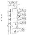
An electronic system shown in Fig. 6 includes avoltage generating circuit 83, which includesvoltage generating circuits voltage generating circuits voltage generating circuits - The electronic system shown in Fig. 6 further includes a VCCQ
power supply line 88, which supplies the power supply voltage VCCQ (= 2 x V5) output from thevoltage generating circuit 83, and atermination voltage line 89, which supplies the termination voltage VTT (= 5 V) output from thevoltage generating circuit 83. Furthermore, the electronic system includes amicroprocessor 90 and SDRAM devices 91 - 94, each of which devices performs an input/output operation on data of eight bits DQ0 - DQ7. Reference numbers 95 - 99 indicate data input/output terminals via which data is input and output. Reference numbers 100 - 104 indicate reference voltage input terminals via which the reference voltage Vref is received. In the first embodiment of the present invention, the termination voltage VTT is supplied, as the reference voltage Vref, to themicroprocessor 90 and the SDRAM devices 91 - 94. - The
microprocessor 90 includes aninput circuit 105 and a push-pull-type output circuit 110, which circuits handle data DQ0. The SDRAM devices 91 - 94 include input circuits 106 - 109 and push-pull-type output circuits 111 - 114, these input and output circuits handling data DQ0. Abus line 115 is provided for transmitting data DQ0.Termination resistors bus line 115. For example, thetermination resistor 116 has a resistance of 50 Ω, and thetermination resistor 117 has a resistance of 30 n. The input and output circuits of themicroprocessor 90 and the SDRAM devices 91 - 94 have an identical circuit configuration, and only the input and output circuit of themicroprocessor 90, which is a part thereof, is illustrated in Fig. 7. - Referring to Fig. 7, the
microprocessor 90 has a VCCpower supply terminal 119 to which the power supply voltage VCC (for example, 3.3 V) is applied, a VCCQpower supply terminal 120 to which the power supply voltage VCCQ (2.0V, for example) is applied, and a VSSpower supply terminal 121 to which the ground voltage VSS (OV) is applied. Themicroprocessor 90 has a VCCpower supply line 122 connected to the VCCpower supply terminal 119, a VCCQpower supply line 123 connected to the VCCQpower supply terminal 120, and a VSSpower supply line 124 connected to the VSSpower supply terminal 121. - The
microprocessor 90 has amain body circuit 125 to which the power supply voltage VCC is applied. The symbol /DATA ("/" is equivalent to the symbol "bar" in Fig. 7) denotes data output from themain body circuit 125, and the symbol /HZ denotes a control signal determining whether the output state should be set to a high-impedance state. Anoutput control circuit 126 is supplied with the power supply voltage VCC, and is made up of a NORcircuit 127, aninverter 128 and aNAND circuit 129. An output driving circuit (pre-driver) 130 is supplied with the power supply voltage VCCQ, and is made up of enhancement-type p-channel MOS transistors channel MOS transistors output circuit 110 is made up of an enhancement-type pMOS transistor 137 serving as a pull-up element, and an enhancement-type nMOS transistor 138 serving as a pull-down element. - In a case where the power supply voltage VCC is supplied, as a back bias voltage, to an N-type well in which the
pMOS transistors pMOS transistors pMOS transistors - With the above in mind, the power supply voltage VCCQ is applied as the back bias voltage to the N-type well in which the
pMOS transistors pMOS transistors pMOS transistors pMOS transistors - Referring to Fig. 8, when the control signal /HZ is low, the output level of the
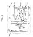
inverter 128 is high and the output level of the NORcircuit 127 is low. Hence, thepMOS transistor 133 is ON and thenMOS transistor 135 is OFF. Further, the output level of aninverter 131 is high, and thus thepMOS transistor 137 is OFF. Further, the output level of theNAND circuit 129 is high, and thepMOS transistor 134 is OFF. ThenMOS transistor 136 is ON, and the output level of aninverter 132 is low. ThenMOS transistor 138 is OFF. Hence, in the above case, theoutput circuit 110 is in the high-impedance state (Hi-Z). - As shown in Fig. 9, when the control signal /HZ is high and data /DATA is high, the output level of the NOR
circuit 127 is low. Hence, thepMOS transistor 133 is ON and thenMOS transistor 135 is OFF. The output level of theinverter 131 is high, and thepMOS transistor 137 is OFF. The output level of theNAND circuit 129 is low, and thepMOS transistor 134 is ON. ThenMOS transistor 136 is OFF, and the output level of theinverter 132 is high. ThenMOS transistor 138 is ON. Hence, the signal DQ0 output from theoutput circuit 110 is low. - As shown in Fig. 10, when the control signal /HZ is high and the data /DATA is low, the output level of the NOR
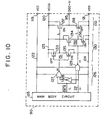
circuit 127 is high. Hence, thepMOS transistor 133 is OFF, and thenMOS transistor 135 is ON. The output level of theinverter 131 is low, and thepMOS transistor 137 is ON. The output level of theNAND circuit 129 is high, and thepMOS transistor 134 is OFF. ThenMOS transistor 136 is ON, and the output level of theinverter 132 is low. ThenMOS transistor 138 is OFF. Hence, in the above case, the signal DQ0 output from theoutput circuit 110 is high. - The SDRAM devices 91 - 94 are connected to the
bus line 115 at equal intervals, and there is provided only thebus line 115 between themicroprocessor 90 and theDRAM device 91. Hence, when the characteristic impedance of thebus line 115 is denoted as Z0, the effective characteristic impedance of parts of thebus line 115 via which the SDRAM devices 91 - 94 are connected at equal intervals are less than that of parts thereof to which the SDRAM devices 91 - 94 are not connected. - Generally, the characteristic impedance Z0 of the
bus line 115 is represented as Z0 = (L/C)1/2 where L is the wiring inductance per unit length, and C is the wiring capacitance per unit length. For example, typically L = 250 nH/m, and C = 100 pF. In this case, Z0 = (250 x 10-9/100 x 10-12)1/2 = 50 Ω. - On the other hand, in the case where the SDRAM devices 91 - 94 are connected, their load capacitances (more particularly, capacitances of the input/output terminals 96 - 99) are added. If the SDRAM devices 91 - 94, each having a capacitance of 3.75 pF, are connected to the
bus line 115 at equal intervals of 6.25 mm, 160 SDRAM devices are connected to the bus line per meter. Assuming that the capacitance per meter is denoted as CL, CL = 3.75 pF x 160 m-1 = 600 pF/m. In this case, the effective characteristic impedance ZL of thebus line 115 is represented as ZL = [L/(C + CL)]1/2, and is equal to 18.9 Ω (= [250 x 10-9/(100 x 10-12 + 600 x 10-12).
This value of the effective characteristic impedance is much less than the characteristic impedance Z0 (= 50 Ω) obtained when there is no load). - In order to strictly establish the impedance matching to thereby avoid any reflection of signals, the resistance values of the
termination resistors termination resistors - With the above in mind, the value of the
termination resistor 117 around which the SDRAM devices 91 - 94 are concentrated is omitted from the strict matching condition, and is made greater than the effective characteristic impedance ZL. The above value is limited to the characteristic impedance Z0 of thebus line 115 with no load connected thereto, more specifically, 30 Ω. - On the other hand, there are not many loads connected to the
microprocessor 90. Hence, the value of thetermination resistor 116 is set equal to 50 Ω, which is equal to the characteristic impedance of thebus line 115 obtained when there is no load. As a result, the load resistance viewed from the driving side is 18.7 Ω, which is equal to the parallel-connection value of 30 Ω and 50 Ω. In this case, the load resistance is greater than that obtained when a resistance of 30 Ω is simply connected on either side of the bus line 115 (the load resistance then being equal to 15 n). Hence, even when the output circuits 110 - 114 have a relatively low current driving capability, it is possible to obtain a large signal amplitude. - The output circuits 110 - 114 of the
microprocessor 90 and the SDRAM devices 91 - 94 are formed with the CMOS-type push-pull circuits to which the power supply voltage VCCQ is applied. Further, the termination voltage VTT is equal to VCCQ/2, and thus the signals can be transmitted in such a way that the center voltage is equal to the termination voltage VTT. - For example, if the
output circuit 110 outputs the low-level output signal, a current flows in a closed circuit made up of thevoltage generating circuit 85, thetermination voltage line 89, thetermination resistors bus line 115, the output circuit 110 (nMOS transistor 138), the ground and thevoltage generating circuit 85 in the above order. - Alternatively, if the
output circuit 110 outputs the high-level output signal, a current flows in a closed circuit made up of thevoltage generating circuit 84, the VCCQpower supply line 88, the output circuit 110 (pMOS transistor 137), thebus line 115, thetermination resistors voltage generating circuit 84 in the above order. - As described above, since the
voltage generating circuits voltage generating circuit 83 are connected in series, the voltage of the voltage output terminal 87 is maintained at V5 equal to 1.0 V even if a current is output or input via the voltage output terminal 87. Hence, it is possible to ensure the stability that the termination voltage VTT is equal to the voltage V5 equal to 1.0 V. - Further, no currents flow in the
termination resistors bus line 115. Hence, power consumption can be reduced. - Furthermore, the termination voltage VTT is used as the reference voltage Vref which is needed in the
microprocessor 90 and the SDRAM devices 91 - 94. Hence, the coincidence of the reference voltage Vref and the termination voltage VTT can be accomplished and no offset voltage is generated. Hence, a sufficient operation margin can be ensured. - Moreover, the power supply voltage VCCQ is supplied as the power supply voltage necessary for the
output driving circuit 130 to drive the output circuits 110 - 114. Hence, it is possible to drive the pMOS transistor serving as the pull-up element and the nMOS transistor serving as the pull-down element in a balanced way. - The
output control circuit 126, theoutput driving circuit 130 and theoutput circuit 110 in themicroprocessor 90 can be configured as shown in Fig. 11. The circuit shown in Fig. 11 can be applied to the SDRAM devices 91 - 94 as well. - In Fig. 11, the
output control circuit 126 is made up of aNAND circuit 141, aninverter 142 and a NORcircuit 143. Theoutput driving circuit 130 is a CMOS type inverter to which the power supply voltage VCC is applied. The CMOS inverter is made up of an enhancementtype pMOS transistor 145 and an enhancementtype nMOS transistor 146. Theoutput circuit 110 is made up of a depletiontype nMOS transistor 147 functioning as a pull-up element and an enhancementtype nMOS transistor 148 functioning as a pull-down element. Theoutput circuit 110 is intended to improve the driving ability of the pull-up element. - In the above case, when the low level of the data signal DQ0 is set equal to V0L in order to make it possible to cut off the depletion
type nMOS transistor 147, it is necessary to set the threshold voltage VTHD of thenMOS transistor 147 to -V0L ≤ VTHD. For example, in the case where the termination voltage VTT is equal to 1.0 V, when the signal DQ0 is within the range of ±0.25 V (driving current is 10 mA), V0L = 1 - 0.25 = 0.75 V. In this case, the threshold voltage VTHD is equal to or greater than -0.75V. - As shown in Fig. 12, when the control signal /HZ is at the high level, the output level of the
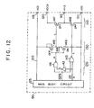
inverter 142 is low, and the output level of theNAND circuit 141 is high. ThepMOS transistor 145 is OFF, and thenMOS transistor 146 is ON. The output level of theinverter 144 is low, and thenMOS transistor 147 is OFF. Further, the output level of the NORcircuit 143 is low, and thenMOS transistor 148 is OFF. In this case, theoutput circuit 110 is in the high-impedance state. - As shown in Fig. 13, when the control signal /HZ is low and the data /DATA is at the high level, the output level of the
NAND circuit 141 is low, and thepMOS transistor 145 is ON. ThenMOS transistor 146 is OFF, the output level of theinverter 144 is high, and thenMOS transistor 147 is ON. Further, the output level of the NORcircuit 143 is low, and thenMOS transistor 148 is OFF. In this case, the signal DQ0 output from theoutput circuit 110 is at the high level. - As shown in Fig. 14, when the control signal /HZ is at the low level and the data /DATA is at the low level, the output level of the
NAND circuit 141 is high, and thepMOS transistor 145 is OFF. ThenMOS transistor 146 is ON, and the output level of theinverter 144 is low. ThenMOS transistor 147 is OFF. Further, the output level of the NORcircuit 143 is high, and thenMOS transistor 148 is ON. In this case, the signal DQ0 output from theoutput circuit 110 is at the low level. - The
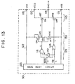
nMOS transistor 147 may be replaced by an enhancement-type nMOS transistor. In this case, unless the threshold voltage of the enhancement type nMOS transistor is lower than the threshold voltage of thenMOS transistor 148, the advantage of an increase in the driving ability may be canceled by a decrease in the threshold voltage. - A description will now be given of an electronic system with reference to Figs. 15 through 19.
- Fig. 15 is a circuit diagram of the essential part of an electronic system.
- The electronic system shown in Fig. 15 has a
voltage generating circuit 150, which generates voltages different from those generated by thevoltage generating circuit 83 shown in Fig. 6. Thevoltage generating circuit 150 hasvoltage generating circuits voltage output terminals voltage generating circuits voltage output terminal 153, and the voltage V6 (= 1.65 V) is output, as the termination voltage VTT, to thevoltage output terminal 154. - The
bus line 115 shown in Fig. 15 has branched parts 155 - 159, that is, stubs. Resistors 160 - 164 are connected between branch points on thebus line 115 and the stubs 155 - 159. - The power supply voltage VCCQ supplied via the VCCQ
power supply line 88 is supplied to the VCC power supply terminals and the VCCQ power supply terminals of themicroprocessor 90 and the SDRAM devices 91 - 94. The VCC power supply terminals of themicroprocessor 90 and the SDRAM devices 91 - 94 are connected to the VCCQ power supply terminals outside thereof. Fig. 16 shows such a connection for themicroprocessor 90. - As shown in Fig. 16 as an example for the
microprocessor 90, according to the second embodiment of the present invention, not only thenain body circuit 125 and theoutput control circuit 126 but also theoutput driving circuit 130 and theoutput circuit 110 are driven by the power supply voltage VCCQ equal to 3.3 V. In this case, the gate of thenMOS transistor 138 is also supplied with the power supply voltage VCCQ of 3.3 V, so that the inner resistance of thenMOS transistor 138 is decreased and an excessive current flows in the output. - With the above in mind, the
resistor 160 is connected between the branching point on thebus line 115 and thestub 155 in order to select an appropriate inner resistance value of theoutput circuit 110 and prevent changes in the driving currents with respect to thetermination resistors bus line 115 and the stubs 156 - 159. - Figs. 17 and 18 show how to determine the resistance values of the resistors 160 - 164. More particularly, Fig. 17 is a graph of the static characteristic of the
nMOS transistor 138 in theoutput circuit 110 of themicroprocessor 90, and Fig. 18 shows part of the configuration shown in Fig. 15. In the second embodiment of the present invention, thenMOS transistor 138 is configured so as to have a static characteristic as shown in Fig. 17. In the case where thenMOS transistor 138 is turned ON with the VCCQ equal to 3.3 V, the gate-source voltage VGS thereof is equal to 3.3 V, while the drain-source voltage VDS thereof is equal to 0.2 V. - Assuming that the driving current for the
nMOS transistor 138 is equal to 10 mA and the resistance values of thetermination resistors termination resistors bus line 115 becomes equal to 1.4 V, which shows that the resistance value of theresistor 160 is determined as 120 Ω (= (1.4 - 0.2)/10 x 10-3). The resistance values of the resistors 161 - 164 are selected in the same way as theresistor 160. - As described above, by providing the resistors 160 - 164 between the
bus line 115 and the stubs 155 - 159, it is possible to minimize the influence of the signal reflection caused in the stubs 155 - 159 to thebus line 115. - In the above case, the characteristic impedances of the stubs 155 - 159 can be determined as follows. First of all, the resistance values of the resistors 160 - 164 are set equal to 120 Ω taking into consideration the driving ability of the output circuit. Since the characteristic impedance of the
bus line 115 is 50 Ω, two resistors having resistances of 50 n connected in parallel are seen when viewing thebus line 115 from the branch node. That is, a characteristic impedance of 25 n can be seen as a load. - Alternatively, when the resistors 160 - 164 respectively have a resistance of 120 n, an impedance of 145 n (= 120 Ω + 25 Ω) can be seen when viewing the
bus line 115 from the stubs 155 - 160. Hence, the characteristic impedances of the stubs 155 - 159 are appropriately set equal to 145 Ω. It has been confirmed through a simulation that the above value causes no problems even when it varies within the range of ±50 %. When the above value of the characteristic impedance of each stub is selected, the signal is input to the stubs 155 - 159 from thebus line 115, the input/output terminals 95 - 99 have no terminations. Hence, the input signal is totally reflected (100% reflection). However, reflection does not take place when the reflected signal is transmitted to the resistors 160 - 164 because the impedance match is established. That is, the signal is absorbed by thetermination resistors bus 115. Hence, thereafter, the resonance phenomenon does not occur after the stubs 155 - 159, and good signal transmissions can be carried out. - When turning ON the
nMOS transistor 138 with VCCQ equal to 2.0 V, the gate-source voltage VGS is equal to 2.0 V, while the drain-source voltage VDS is equal to 0.75 V. Sine the driving current for thenMOS transistor 138 is equal to 10 mA, the resistances of thetermination resistors termination resistors resistor 160 is not needed. That is, when decreasing the power supply voltage VCCQ, the resistors 160 - 164 are needed no longer, and the number of parts can be reduced.
However, the resonances caused in the stubs 155 - 159 cannot be suppressed by means of impedance matching. Hence, it is necessary to reduce the lengths of the stubs 155 - 159 as much as possible. - The output circuits 110 - 114 of the
microprocessor 90 and the SDRAM devices 91 - 94 are formed by the CMOS type push-pull circuits supplied with the power supply voltage VCCQ. Further, the termination voltage VTT is set to VCCQ/2. Hence, it is possible to transmit small-amplitude signals having the center voltage equal to the termination voltage VTT. - When the
output circuit 110 provides the low level, a current flows, in the following order, in a closed circuit made up of thevoltage generating circuit 152, thetermination voltage line 89, thetermination resistors bus line 115, the output circuit 110 (nMOS transistor 138), the ground and thevoltage generating circuit 152. When theoutput circuit 110 provides the high level, a current flows in a closed circuit made up of thevoltage generating circuit 151, the VCCQpower supply line 88, the output circuit 110 (pMOS transistor 137), thebus line 115, thetermination resistors voltage generating circuit 151. - As described above, since the
voltage generating circuits voltage output terminal 154 or flows therein. Hence, it becomes possible to ensure the stability in which VTT = V6 = 1.65 V. - Further, no currents flow in the
termination resistors bus line 115. Hence, power consumption can be reduced. - Furthermore, the termination voltage VTT is used as the reference voltage Vref which is needed in the
microprocessor 90 and the SDRAM devices 91 - 94. Hence, the coincidence of the reference voltage Vref and the termination voltage VTT can be accomplished and no offset voltage is generated. Hence, the sufficient operation margin can be ensured. - Moreover, the resistors 160 - 164 are provided at the branch points on the
bus line 115. Hence, it is possible to not only prevent an excessive current from flowing in the circuits but also to cut off, by means of the resistors 160 - 164, highfrequency components contained in the reflected signals produced at the stubs 155 - 159 in the case where these stubs are needed. As a result, it is difficult for the transmitted signal waveforms to be deformed. From these viewpoints, it can be said that the second embodiment of the present invention is suitable for a system in which the SDRAM devices 91 - 94 are mounted on a module (SIMM) and connectors of the module are connected to thebus line 115. Meanwhile, the structure is suitable for a system in which the SDRAM devices 91 - 95 are directly connected to thebus line 115 because it does not need the stubs 155 - 159. - Fig. 19A is a circuit diagram of a practical example of the
voltage generating circuit 150 shown in Fig. 15. The circuit shown in Fig. 19A is a switching regulator. Thevoltage generating circuit 150 shown in Fig. 19A includes a pMOS transistor Q1, an nMOS transistor Q2, diodes D1 and D2, an inductor L, capacitors C1 and C2, and acontrol circuit 150A. Thecontrol circuit 150A includes a comparator COMP and a driver DRV having two CMOS inverters. - The transistors Q1 and Q2 function as switches of the switching regulator. The diodes D1 and D2 allow a counter electromotive force of the inductance to pass therethrough. The inductor L and the capacitors C1 and C2 form a smoothing circuit. The voltage of the
output terminal 154 is compared with the reference voltage VREF (= VCC/2 = 1.65 V in this example), and the output signal of the comparator COMP drives the transistors Q1 and Q2. When no load current flows, the comparator output turns ON and OFF the transistors Q1 and Q2 with the equal duty ratio. In this state, the circuit is in the oscillating state. Thecontrol circuit 150A can be formed by Si9145 manufactured by Siliconics in the United States. - The
voltage generating circuit 83 shown in Fig. 6 can be configured in the same way as described above. - A description will now be given of an electronic system with reference to Fig. 20.
- Fig. 20 is a circuit diagram of the essential part of an electronic system. In the structure shown in Fig. 20, the resistors 161 - 164 are connected between the
bus line 115 and the stubs 156 - 159, while no resistor is intentionally connected between themicroprocessor 90 and thebus line 115. - When the SDRAM devices 91 - 94 are mounted on the SIMM, it is easy to provide the
bus line 115 and the stubs 155 - 159. However, in many cases, themicroprocessor 90 is mounted on PGA (Pin Grid Array) packages and has a large number of pins. Hence, many cases will take place in which no space for providing theresistor 160 shown in Fig. 15 is available. - With the above in mind, the resistors 161 - 164 are connected between the
bus line 115 and the stubs 156 - 159, while theresistor 160 shown in Fig. 15 is not provided between thebus line 115 and theprocessor 90. Even when theresistor 160 is not used, themicroprocessor 90 would be connected to an end portion of thebus line 115 in many cases. This end portion is close to thetermination resistor 116, which functions to reduce deformation in the signal waveforms. - Further, in the above case, an excessive current will not flow in the circuits if the
output circuit 110 of themicroprocessor 90 is designed to have a small driving ability and the inner resistance thereof is as high as approximately 100 Ω. The decreasing of the inner resistance of theoutput circuit 110 to approximately 100 Ω can be achieved by adjusting the sizes of thepMOS transistor 137 and thenMOS transistor 138, or providing a resistor in series to the output of theoutput circuit 110 at a position close to theoutput circuit 110, for example, on the chip or in the package. - When the sizes of the
pMOS transistor 137 and thenMOS transistor 138 are adjusted, the gate width of thepMOS transistor 137 is set to, for example, 500 µm and the gate length thereof is set to, for example, 1 µm. Further, the gate width of thenMOS transistor 138 is set to, for example, 200 µm, and the gate length thereof is set to, for example, 1 µm. - When a resistor is connected in series to the output of the
output circuit 110, the gate width and gate length of thepMOS transistor 137 are set to, for example, 1000 µm and 1 µm, respectively. Further, the gate width and gate length of thenMOS transistor 138 are set to, for example, 400 µm and 1 µm, respectively. - If the resistor connected in series to the
output circuit 110 has a negative temperature coefficient, it advantageously functions to cancel a positive temperature coefficient of the inner resistances of the transistors of theoutput circuit 110. For example, it is possible to make the series-connected resistor of an amorphous-system semiconductor material generally called thermistor. As a simpler method, the series-connected resistor is formed by a diffused layer formed in a semiconductor substrate. The p-type diffused layer has a temperature coefficient greater than that of the n-type diffused layer. Such diffused layers are suitable for the above purpose. The above-mentioned materials have natures in which the resistance is decreased as the temperature increases. Hence, it is possible to cancel a phenomenon such that the driving abilities of transistors are decreased as the temperature increases. - A description will now be given of another electronic system with reference to Fig. 21.
- Fig. 21 is a circuit diagram of the essential part of an electronic system.
- In the structure shown in Fig. 21, a
temperature sensor 165 is provided to control the voltage V6 generated by thevoltage generating circuits - It is necessary to pay attention to the temperature dependence of the driving ability of the
output circuit 110 of themicroprocessor 90 in the following case. That is, the resistors 161 - 164 are connected between thebus line 115 and the stubs 156 - 159, and no resistor is connected to thebus line 115 and themicroprocessor 90. Further, the transistors in theoutput circuit 110 of themicroprocessor 90 have small driving abilities. It should be noted that the MOS transistors have negative driving current temperature coefficients, in which the driving ability is degraded as the operation temperature increases. - With the above in mind, in order to maintain a constant signal amplitude on the
bus line 115 independent of the operation temperature, it is suitable to make the voltage V6 output from thevoltage generating circuits - It is possible to design the system so that the power supply voltage for only the input/output circuit depends on the temperature, and the power supply voltage for the main body circuit is maintained at the constant level. It is also possible to design the system so that the power supply voltages of both the input/output circuit and the main body circuit depend on the temperature. The above temperature compensation can be applied irrespective of whether any resistor is connected to the
bus line 115. - A description will now be given, with reference to Figs. 22 through 24, of an electronic system according to an embodiment of the present invention.
- Fig. 22 is a circuit diagram of the essential part of the electronic system according to the embodiment of the present invention. In the structure shown in Fig. 22, the
voltage generating circuit 83 shown in Fig. 6 is replaced by a terminationvoltage generating circuit 166. Correspondingly, there are provided a VCCQpower supply line 167 for supplying the power supply voltage VCCQ equal to 2.0 V to the terminationvoltage generating circuit 166, and a VSSQpower supply line 168 for supplying the power. supply voltage VSSQ equal to 0 V to the terminationvoltage generating circuit 166. - In the embodiment of the present invention, the power supply voltage VCCQ from the VCCQ
power supply line 167 is supplied to themicroprocessor 90 and the SDRAM devices 91 - 94. The other parts of the circuit of the embodiment of the present invention are the same as those shown in Fig. 6. - The termination
voltage generating circuit 166 includes anoperational amplifier 171, andvoltage dividing resistors resistors operational amplifier 171. The output of theoperational amplifier 171 is fed back to the reverse phase (inverting) input terminal of theoperational amplifier 171. Thereby, the termination voltage VTT equal to VCCQ/2 is obtained at the output terminal of theoperational amplifier 171. - There are integrally provided on one chip the termination
voltage generating circuit 166, thevoltage dividing resistors termination resistor 117 for thebus line 115 provided for the data DQ0, and termination resistors for the bus lines for data DQ1 - DQ7. These elements provided on one chip are packaged, as a termination module (termination device), with the same dimensions as the SDRAM devices 91 - 94. - Fig. 23 schematically shows the
termination module 174, which includes a termination modulemain body 175, termination resistors 176 - 181 respectively provided for data DQ1 - DQ7 and external terminals 182 - 200. These external terminals 182 - 200 are located in the same positions of the corresponding external terminals of each of the SDRAM device 91 - 94. - Fig. 24 is a circuit diagram of the termination
voltage generating circuit 166 used in the embodiment of the present invention. Thecircuit 166 includes a VCCQpower supply line 211, a VSSQpower supply line 212, anddifferential amplifier circuits differential amplifier circuit 213 includes enhancementtype pMOS transistors circuit 166 includes enhancementtype nMOS transistors 217 and 218 functioning as driving transistors, and an enhancementtype nMOS transistor 219 functioning as a resistor. - The
differential amplifier circuit 214 includes an enhancementtype pMOS transistor 220 functioning as a resistor, enhancementtype pMOS transistors nMOS transistors voltage generating circuit 166 shown in Fig. 24 includes anoutput circuit 225, which is made up of an enhancementtype pMOS transistor 226 functioning as a pull-up element, and an enhancementtype nMOS transistor 227 functioning as a pull-down element.
Claims (1)
- An electronic system comprising:a plurality of electronic circuits (68,77) each having a signal input and output function;a bus (75) to which the plurality of electronic circuits are connected;first termination resistors (76) connected to ends of the bus; anda termination voltage circuit having a first part (58) generating a first voltage (V3) and a second part (60) generating a second voltage (V4), the first voltage (V3)being supplied, as a power supply voltage, to output circuits (72) of the plurality of electronic circuits connected to the bus, the second voltage (V4) being supplied to the first termination resistors (76) as a termination voltage (VTT),characterized in that
the second part (60) comprises an operational amplifier (63, 171) having a first input terminal receiving a divided voltage derived from the first voltage (V3), a
second input terminal, and an output terminal connected to the second input terminal; and
the second voltage (V4) is output via said output terminal and is equal to the divided voltage derived from the first voltage,
wherein said operational amplifier (171) comprises:a first differential amplifier circuit (213) supplied, as a power supply voltage, with said first voltage and comprised of driving transistors formed of first and second n-channel insulation gate type field effect transistors (218, 217);a second differential amplifier circuit (214) supplied, as a power supply voltage, with said first voltage and comprised of driving transistors formed of first and second p-channel insulation gate type field effect transistors (222,221); andan output circuit (225) supplied, as a power supply voltage, with said first voltage and comprised of a pull-up element driven by said first differential amplifier circuit (213) and formed of a third p-channel insulation gate type field effect transistor (226) and a pull-down element driven by said second differential amplifier circuit (214) and formed of a third n-channel insulation gate type field effect transistor (227),wherein:a connection node at which a gate of the first p-channel insulation gate type field effect transistor (222) and a gate of the first n-channel insulation gate type field effect transistor (218) are connected together is connected to said first input terminal;a connection node at which a gate of the second p-channel insulation gate type field effect transistor (221) and a gate of the second n-channel insulation gate type field effect transistor (217) are connected together is connected to said second input terminal; andan output terminal of said output circuit (225) of the operational amplifier (171) forms the output terminal of the operational amplifier.
Applications Claiming Priority (7)
| Application Number | Priority Date | Filing Date | Title |
|---|---|---|---|
| JP29766993 | 1993-11-29 | ||
| JP29766993A JP3170980B2 (en) | 1993-11-29 | 1993-11-29 | Semiconductor integrated circuit |
| JP3047094 | 1994-02-28 | ||
| JP03050194A JP3147642B2 (en) | 1994-02-28 | 1994-02-28 | Electronic devices, integrated circuits and termination devices |
| JP03047094A JP3146829B2 (en) | 1994-02-28 | 1994-02-28 | Semiconductor integrated circuit |
| JP3050194 | 1994-02-28 | ||
| EP94118585A EP0655839B1 (en) | 1993-11-29 | 1994-11-25 | Electronic system for terminating bus lines |
Related Parent Applications (1)
| Application Number | Title | Priority Date | Filing Date |
|---|---|---|---|
| EP94118585A Division EP0655839B1 (en) | 1993-11-29 | 1994-11-25 | Electronic system for terminating bus lines |
Publications (2)
| Publication Number | Publication Date |
|---|---|
| EP1564947A1 EP1564947A1 (en) | 2005-08-17 |
| EP1564947B1 true EP1564947B1 (en) | 2006-12-27 |
Family
ID=27286971
Family Applications (3)
| Application Number | Title | Priority Date | Filing Date |
|---|---|---|---|
| EP94118585A Expired - Lifetime EP0655839B1 (en) | 1993-11-29 | 1994-11-25 | Electronic system for terminating bus lines |
| EP05009867A Expired - Lifetime EP1564947B1 (en) | 1993-11-29 | 1994-11-25 | Electronic system for terminating bus lines |
| EP03025514A Withdrawn EP1392028A1 (en) | 1993-11-29 | 1994-11-25 | Driver with complementary gates |
Family Applications Before (1)
| Application Number | Title | Priority Date | Filing Date |
|---|---|---|---|
| EP94118585A Expired - Lifetime EP0655839B1 (en) | 1993-11-29 | 1994-11-25 | Electronic system for terminating bus lines |
Family Applications After (1)
| Application Number | Title | Priority Date | Filing Date |
|---|---|---|---|
| EP03025514A Withdrawn EP1392028A1 (en) | 1993-11-29 | 1994-11-25 | Driver with complementary gates |
Country Status (5)
| Country | Link |
|---|---|
| US (2) | US6160417A (en) |
| EP (3) | EP0655839B1 (en) |
| KR (1) | KR0157096B1 (en) |
| CN (2) | CN1158611C (en) |
| DE (2) | DE69434903T2 (en) |
Families Citing this family (65)
| Publication number | Priority date | Publication date | Assignee | Title |
|---|---|---|---|---|
| US5546016A (en) * | 1995-07-03 | 1996-08-13 | Intel Corporation | MOS termination for low power signaling |
| JP3195913B2 (en) * | 1996-04-30 | 2001-08-06 | 株式会社東芝 | Semiconductor integrated circuit device |
| CN100356362C (en) * | 1996-06-07 | 2007-12-19 | 株式会社日立制作所 | Signal transmission system |
| JP2910679B2 (en) * | 1996-07-04 | 1999-06-23 | 日本電気株式会社 | Semiconductor integrated circuit |
| GB2322042B (en) * | 1997-02-05 | 2002-02-06 | Ericsson Telefon Ab L M | Radio architecture |
| TW381385B (en) * | 1997-08-20 | 2000-02-01 | Advantest Corp | Signal transmission circuit, CMOS semiconductor device and circuit board |
| WO1999053627A1 (en) | 1998-04-10 | 1999-10-21 | Chrimar Systems, Inc. Doing Business As Cms Technologies | System for communicating with electronic equipment on a network |
| AU2439999A (en) * | 1998-04-23 | 1999-11-08 | Matsushita Electric Industrial Co., Ltd. | Method of designing power supply circuit and semiconductor chip |
| JP2000012787A (en) * | 1998-06-10 | 2000-01-14 | Lucent Technol Inc | Integrated circuit device and method for forming resistance elements used in integrated circuit |
| US6067596A (en) * | 1998-09-15 | 2000-05-23 | Compaq Computer Corporation | Flexible placement of GTL end points using double termination points |
| US6108740A (en) * | 1998-10-14 | 2000-08-22 | Lsi Logic Corporation | Method and apparatus for terminating a bus such that stub length requirements are met |
| US6222389B1 (en) | 1999-03-25 | 2001-04-24 | International Business Machines Corporation | Assisted gunning transceiver logic (AGTL) bus driver |
| US6212591B1 (en) | 1999-04-02 | 2001-04-03 | Cradle Technologies | Configurable I/O circuitry defining virtual ports |
| JP3849835B2 (en) * | 1999-06-23 | 2006-11-22 | 株式会社ルネサステクノロジ | Semiconductor integrated circuit device |
| JP2001068626A (en) * | 1999-08-27 | 2001-03-16 | Mitsubishi Electric Corp | Semiconductor device |
| US6380787B1 (en) * | 1999-08-31 | 2002-04-30 | Micron Technology, Inc. | Integrated circuit and method for minimizing clock skews |
| US6271704B1 (en) * | 1999-12-14 | 2001-08-07 | Intel Corporation | Method and apparatus for balancing current in a system with two sets of termination devices |
| US6356106B1 (en) * | 2000-09-12 | 2002-03-12 | Micron Technology, Inc. | Active termination in a multidrop memory system |
| KR100340285B1 (en) * | 2000-10-24 | 2002-06-15 | 윤종용 | Memory module having series-connected printed circuit boards |
| US6323687B1 (en) | 2000-11-03 | 2001-11-27 | Fujitsu Limited | Output drivers for integrated-circuit chips with VCCQ supply compensation |
| JP2002251890A (en) * | 2001-02-26 | 2002-09-06 | Mitsubishi Electric Corp | Signal amplifier circuit and semiconductor memory provided therewith |
| GB2386484A (en) * | 2002-03-14 | 2003-09-17 | Sharp Kk | Level shifting and active matrix driver |
| US7280574B1 (en) * | 2002-05-15 | 2007-10-09 | Cypress Semiconductor Corp. | Circuit for driving a laser diode and method |
| JP2004039689A (en) * | 2002-06-28 | 2004-02-05 | Sony Corp | Electronic circuit device |
| US6836142B2 (en) * | 2002-07-12 | 2004-12-28 | Xilinx, Inc. | Asymmetric bidirectional bus implemented using an I/O device with a digitally controlled impedance |
| US6963218B1 (en) * | 2002-08-09 | 2005-11-08 | Xilinx, Inc. | Bi-directional interface and communication link |
| US6922071B2 (en) * | 2002-12-27 | 2005-07-26 | Intel Corporation | Setting multiple chip parameters using one IC terminal |
| FR2849972B1 (en) * | 2003-01-10 | 2005-03-04 | Somfy Sas | INSTALLATION FOR EXCHANGING INFORMATION BETWEEN A TRANSMITTER AND A RECEIVER. |
| US6922076B2 (en) * | 2003-08-27 | 2005-07-26 | International Business Machines Corporation | Scalable termination |
| DE10352812B4 (en) * | 2003-11-12 | 2008-08-14 | Infineon Technologies Ag | Method and circuit arrangement for generating ternary signals |
| JP4275583B2 (en) * | 2004-06-24 | 2009-06-10 | ユーディナデバイス株式会社 | Electronic module |
| US7242249B2 (en) * | 2005-02-11 | 2007-07-10 | International Business Machines Corporation | Peaking transmission line receiver for logic signals |
| KR100697281B1 (en) | 2005-03-17 | 2007-03-20 | 삼성전자주식회사 | Method and Apparatus for Preventing the Impedance mismatch and Voltage drop due to the Variations of Package Resistance in Receiver |
| US7358758B2 (en) * | 2005-10-18 | 2008-04-15 | Via Technologies, Inc. | Apparatus and method for enabling a multi-processor environment on a bus |
| JP2007227625A (en) * | 2006-02-23 | 2007-09-06 | Toshiba Microelectronics Corp | Semiconductor integrated circuit and its layout designing method |
| US20080270037A1 (en) * | 2007-04-30 | 2008-10-30 | Masato Nakada | System and method for measuring and displaying health information |
| US7646213B2 (en) * | 2007-05-16 | 2010-01-12 | Micron Technology, Inc. | On-die system and method for controlling termination impedance of memory device data bus terminals |
| CN101675632B (en) * | 2007-06-05 | 2012-11-21 | 松下电器产业株式会社 | Receiver circuit and data transmission system |
| US20090091963A1 (en) * | 2007-10-04 | 2009-04-09 | Advanced Micro Devices, Inc. | Memory device |
| US7750666B2 (en) * | 2008-09-15 | 2010-07-06 | Integrated Device Technology, Inc. | Reduced power differential type termination circuit |
| US7767492B1 (en) | 2009-04-14 | 2010-08-03 | Via Technologies, Inc. | Location-based bus termination for multi-core/multi-package processor configurations |
| US8242802B2 (en) * | 2009-04-14 | 2012-08-14 | Via Technologies, Inc. | Location-based bus termination for multi-core processors |
| US7843225B2 (en) * | 2009-04-14 | 2010-11-30 | Via Technologies, Inc. | Protocol-based bus termination for multi-core processors |
| US8085062B2 (en) * | 2009-04-14 | 2011-12-27 | Via Technologies, Inc. | Configurable bus termination for multi-core/multi-package processor configurations |
| JP5726635B2 (en) * | 2010-08-25 | 2015-06-03 | 株式会社Nttドコモ | Multi-mode front-end circuit |
| CN102243481B (en) * | 2011-03-28 | 2013-04-24 | 上海华为技术有限公司 | Device, method and circuit for realizing interconnection between modules powered by different power supplies |
| US8848462B2 (en) * | 2011-10-11 | 2014-09-30 | Mediatek Inc. | Low power memory controllers |
| US10698432B2 (en) | 2013-03-13 | 2020-06-30 | Intel Corporation | Dual loop digital low drop regulator and current sharing control apparatus for distributable voltage regulators |
| US10153611B2 (en) | 2015-04-09 | 2018-12-11 | Hewlett Packard Enterprise Development Lp | Termination voltage circuits |
| CN104882869A (en) * | 2015-06-11 | 2015-09-02 | 国网四川省电力公司南充供电公司 | Mobile device data interface protective circuit |
| FI20150294A (en) * | 2015-10-23 | 2017-04-24 | Ari Paasio | Low power logic family |
| US10348270B2 (en) | 2016-12-09 | 2019-07-09 | Micron Technology, Inc. | Apparatuses and methods for calibrating adjustable impedances of a semiconductor device |
| JP2018133503A (en) * | 2017-02-16 | 2018-08-23 | 東芝メモリ株式会社 | Semiconductor storage device |
| CN107277660B (en) * | 2017-06-07 | 2019-10-15 | 上海乐野网络科技有限公司 | A kind of ear electric discharge road for improving dynamic range and slew rate |
| US10193711B2 (en) | 2017-06-22 | 2019-01-29 | Micron Technology, Inc. | Timing based arbitration methods and apparatuses for calibrating impedances of a semiconductor device |
| KR102347178B1 (en) * | 2017-07-19 | 2022-01-04 | 삼성전자주식회사 | Terminal device having reference voltage circuit |
| US10615798B2 (en) | 2017-10-30 | 2020-04-07 | Micron Technology, Inc. | Apparatuses and methods for identifying memory devices of a semiconductor device sharing an external resistance |
| CN108540295B (en) * | 2018-04-10 | 2021-05-07 | 武汉虹创联众科技有限公司 | Single-bus communication circuit |
| US10916288B1 (en) * | 2019-07-18 | 2021-02-09 | Micron Technology, Inc. | Sensing techniques for a memory cell |
| US10729002B2 (en) * | 2019-07-18 | 2020-07-28 | Intel Corporation | Device, system and method to mitigate signal noise in communications with a memory module |
| US10747245B1 (en) | 2019-11-19 | 2020-08-18 | Micron Technology, Inc. | Apparatuses and methods for ZQ calibration |
| US10892759B1 (en) * | 2020-02-19 | 2021-01-12 | Amazing Microelectronic Corp. | Bus driver module with controlled circuit and transition controlled circuit thereof |
| CN111586969B (en) * | 2020-04-28 | 2021-12-21 | 中国科学院计算技术研究所 | Circuit wiring method, DDR4 internal memory circuit and electronic equipment |
| JP2022088984A (en) * | 2020-12-03 | 2022-06-15 | 株式会社日立製作所 | Control device |
| JP2024522244A (en) * | 2021-05-07 | 2024-06-11 | ブルーマインド インコーポレイテッド | Systems, methods, and computer devices for transistor-based neural networks |
Citations (1)
| Publication number | Priority date | Publication date | Assignee | Title |
|---|---|---|---|---|
| DE4142081A1 (en) * | 1990-12-20 | 1992-07-23 | Murata Manufacturing Co | TERMINAL CIRCUIT TO TERMINATE A DATA BUS |
Family Cites Families (22)
| Publication number | Priority date | Publication date | Assignee | Title |
|---|---|---|---|---|
| US3631528A (en) * | 1970-08-14 | 1971-12-28 | Robert S Green | Low-power consumption complementary driver and complementary bipolar buffer circuits |
| JPS59117323A (en) * | 1982-12-23 | 1984-07-06 | Mitsubishi Electric Corp | Resistor module |
| US4591745A (en) * | 1984-01-16 | 1986-05-27 | Itt Corporation | Power-on reset pulse generator |
| US4647797A (en) * | 1984-08-23 | 1987-03-03 | Ncr Corporation | Assist circuit for improving the rise time of an electronic signal |
| US4766334A (en) * | 1986-03-07 | 1988-08-23 | The Singer Company | Level clamp for Tri-state CMOS bus structure |
| JPS6342215A (en) * | 1986-08-07 | 1988-02-23 | Canon Inc | Electronic equipment |
| JPH0728214B2 (en) * | 1987-02-06 | 1995-03-29 | 株式会社日立製作所 | Semiconductor integrated circuit device |
| US4871931A (en) * | 1987-10-30 | 1989-10-03 | Gazelle Microcircuits, Inc. | Logic circuit resistant to errors due to supply fluctuations |
| US4808855A (en) * | 1987-12-16 | 1989-02-28 | Intel Corporation | Distributed precharge wire-or bus |
| JP2573320B2 (en) * | 1988-07-11 | 1997-01-22 | 株式会社東芝 | Output buffer circuit |
| US5019729A (en) * | 1988-07-27 | 1991-05-28 | Kabushiki Kaisha Toshiba | TTL to CMOS buffer circuit |
| GB2234872B (en) * | 1989-08-03 | 1994-04-06 | Plessey Co Plc | High speed CMOS differential interface circuits |
| IT1231052B (en) * | 1989-09-27 | 1991-11-12 | Bull Hn Information Syst | SWITCHING POWER SUPPLY WITH MULTIPLE OUTPUTS, ADJUSTING AN OUTPUT VOLTAGE AND LOAD COMPENSATION. |
| US4994690A (en) * | 1990-01-29 | 1991-02-19 | Motorola, Inc. | Split level bus |
| US5132564A (en) * | 1990-07-27 | 1992-07-21 | North American Philips Corp. | Bus driver circuit with low on-chip dissipation and/or pre-biasing of output terminal during live insertion |
| JPH04150731A (en) * | 1990-10-09 | 1992-05-25 | Matsushita Electric Ind Co Ltd | Power supply |
| US5266847A (en) * | 1990-12-28 | 1993-11-30 | National Semiconductor Corporation | High speed data transceiver |
| US5149992A (en) * | 1991-04-30 | 1992-09-22 | The State Of Oregon Acting By And Through The State Board Of Higher Education On Behalf Of Oregon State University | MOS folded source-coupled logic |
| EP0533971A1 (en) * | 1991-09-24 | 1993-03-31 | Siemens Aktiengesellschaft | Interface circuit |
| US5227677A (en) * | 1992-06-10 | 1993-07-13 | International Business Machines Corporation | Zero power transmission line terminator |
| US5347177A (en) * | 1993-01-14 | 1994-09-13 | Lipp Robert J | System for interconnecting VLSI circuits with transmission line characteristics |
| US5471498A (en) * | 1993-04-15 | 1995-11-28 | National Semiconductor Corporation | High-speed low-voltage differential swing transmission line transceiver |
-
1994
- 1994-11-25 DE DE69434903T patent/DE69434903T2/en not_active Expired - Fee Related
- 1994-11-25 EP EP94118585A patent/EP0655839B1/en not_active Expired - Lifetime
- 1994-11-25 DE DE69434906T patent/DE69434906T2/en not_active Expired - Fee Related
- 1994-11-25 EP EP05009867A patent/EP1564947B1/en not_active Expired - Lifetime
- 1994-11-25 EP EP03025514A patent/EP1392028A1/en not_active Withdrawn
- 1994-11-28 CN CNB941189724A patent/CN1158611C/en not_active Expired - Fee Related
- 1994-11-28 CN CNB031430554A patent/CN1271531C/en not_active Expired - Fee Related
- 1994-11-28 US US08/351,064 patent/US6160417A/en not_active Expired - Fee Related
- 1994-11-29 KR KR1019940032390A patent/KR0157096B1/en not_active IP Right Cessation
-
1996
- 1996-09-10 US US08/715,358 patent/US5729154A/en not_active Expired - Fee Related
Patent Citations (1)
| Publication number | Priority date | Publication date | Assignee | Title |
|---|---|---|---|---|
| DE4142081A1 (en) * | 1990-12-20 | 1992-07-23 | Murata Manufacturing Co | TERMINAL CIRCUIT TO TERMINATE A DATA BUS |
Non-Patent Citations (1)
| Title |
|---|
| DR.-ING. WILLI RYCHETSKY: "Entwurf elektronischer Schaltungen I, Wintersemester 1971/72", 1971, TECHNISCHE HOCHSCHULE DARMSTADT, FACHBEREICH NACHRICHTENTECHNIK, DARMSTADT * |
Also Published As
| Publication number | Publication date |
|---|---|
| KR0157096B1 (en) | 1999-02-18 |
| CN1271531C (en) | 2006-08-23 |
| DE69434906D1 (en) | 2007-02-15 |
| DE69434903D1 (en) | 2007-02-08 |
| US6160417A (en) | 2000-12-12 |
| CN1117614A (en) | 1996-02-28 |
| EP0655839A3 (en) | 1996-07-17 |
| US5729154A (en) | 1998-03-17 |
| KR950016005A (en) | 1995-06-17 |
| EP1392028A1 (en) | 2004-02-25 |
| DE69434903T2 (en) | 2007-04-26 |
| EP0655839A2 (en) | 1995-05-31 |
| DE69434906T2 (en) | 2007-08-30 |
| CN1516028A (en) | 2004-07-28 |
| EP0655839B1 (en) | 2007-01-03 |
| EP1564947A1 (en) | 2005-08-17 |
| CN1158611C (en) | 2004-07-21 |
Similar Documents
| Publication | Publication Date | Title |
|---|---|---|
| EP1564947B1 (en) | Electronic system for terminating bus lines | |
| EP0905902B1 (en) | Constant current cmos output driver circuit with dual gate transistor devices | |
| KR100932548B1 (en) | Calibration Circuit with On Die Termination Device | |
| US7990178B2 (en) | Driving circuit with impedence calibration | |
| US5550496A (en) | High speed I/O circuit having a small voltage swing and low power dissipation for high I/O count applications | |
| CN100592424C (en) | Methods and circuits for generating reference voltage | |
| US6985009B2 (en) | Signal transmitting system | |
| US7579882B2 (en) | Output buffer circuit eliminating high voltage insulated transistor and level shift circuit, and an electronic device using the output buffer circuit | |
| JPH1185345A (en) | Input/output interface circuit and semiconductor system | |
| JPH07183774A (en) | Output buffer circuit, input buffer circuit and input/ output buffer circuit | |
| JP2010178346A (en) | Output buffer having predriver for compensating slew rate against process variation | |
| US5514983A (en) | CMOS full duplex transmission-reception circuit | |
| JP4676646B2 (en) | Impedance adjustment circuit and semiconductor device | |
| US6766155B2 (en) | Fixed termination scheme for differential receiver that compensates for process, voltage, and temperature variations | |
| US6060905A (en) | Variable voltage, variable impedance CMOS off-chip driver and receiver interface and circuits | |
| US20060061395A1 (en) | Semiconductor integrated circuit | |
| US5646549A (en) | Semiconductor device having an output circuit for transmitting low-voltage differential signals | |
| JP3147642B2 (en) | Electronic devices, integrated circuits and termination devices | |
| Esch et al. | Theory and design of CMOS HSTL I/O pads | |
| KR100354672B1 (en) | Level-shifting circuit and input and output circuits using the same | |
| JP2910679B2 (en) | Semiconductor integrated circuit | |
| KR100293303B1 (en) | Input buffer for semiconductor device | |
| KR100924016B1 (en) | Calibration circuit of On Die Termination Device | |
| KR100861180B1 (en) | Semiconductor memory device | |
| KR20010062003A (en) | Buffer circuit |
Legal Events
| Date | Code | Title | Description |
|---|---|---|---|
| PUAI | Public reference made under article 153(3) epc to a published international application that has entered the european phase |
Free format text: ORIGINAL CODE: 0009012 |
|
| AC | Divisional application: reference to earlier application |
Ref document number: 0655839 Country of ref document: EP Kind code of ref document: P |
|
| AK | Designated contracting states |
Kind code of ref document: A1 Designated state(s): DE FR GB IT |
|
| RIN1 | Information on inventor provided before grant (corrected) |
Inventor name: TAGUCHI, MASAO,C/O FUJITSU LIMITED |
|
| 17P | Request for examination filed |
Effective date: 20050726 |
|
| AKX | Designation fees paid |
Designated state(s): DE FR GB IT |
|
| GRAP | Despatch of communication of intention to grant a patent |
Free format text: ORIGINAL CODE: EPIDOSNIGR1 |
|
| RTI1 | Title (correction) |
Free format text: ELECTRONIC SYSTEM FOR TERMINATING BUS LINES |
|
| GRAS | Grant fee paid |
Free format text: ORIGINAL CODE: EPIDOSNIGR3 |
|
| GRAA | (expected) grant |
Free format text: ORIGINAL CODE: 0009210 |
|
| AC | Divisional application: reference to earlier application |
Ref document number: 0655839 Country of ref document: EP Kind code of ref document: P |
|
| AK | Designated contracting states |
Kind code of ref document: B1 Designated state(s): DE FR GB IT |
|
| REG | Reference to a national code |
Ref country code: GB Ref legal event code: FG4D |
|
| REF | Corresponds to: |
Ref document number: 69434903 Country of ref document: DE Date of ref document: 20070208 Kind code of ref document: P |
|
| ET | Fr: translation filed | ||
| PLBE | No opposition filed within time limit |
Free format text: ORIGINAL CODE: 0009261 |
|
| STAA | Information on the status of an ep patent application or granted ep patent |
Free format text: STATUS: NO OPPOSITION FILED WITHIN TIME LIMIT |
|
| 26N | No opposition filed |
Effective date: 20070928 |
|
| PGFP | Annual fee paid to national office [announced via postgrant information from national office to epo] |
Ref country code: DE Payment date: 20081120 Year of fee payment: 15 |
|
| PGFP | Annual fee paid to national office [announced via postgrant information from national office to epo] |
Ref country code: IT Payment date: 20081126 Year of fee payment: 15 |
|
| PGFP | Annual fee paid to national office [announced via postgrant information from national office to epo] |
Ref country code: FR Payment date: 20081112 Year of fee payment: 15 |
|
| PGFP | Annual fee paid to national office [announced via postgrant information from national office to epo] |
Ref country code: GB Payment date: 20081119 Year of fee payment: 15 |
|
| GBPC | Gb: european patent ceased through non-payment of renewal fee |
Effective date: 20091125 |
|
| REG | Reference to a national code |
Ref country code: FR Ref legal event code: ST Effective date: 20100730 |
|
| PG25 | Lapsed in a contracting state [announced via postgrant information from national office to epo] |
Ref country code: FR Free format text: LAPSE BECAUSE OF NON-PAYMENT OF DUE FEES Effective date: 20091130 |
|
| PG25 | Lapsed in a contracting state [announced via postgrant information from national office to epo] |
Ref country code: DE Free format text: LAPSE BECAUSE OF NON-PAYMENT OF DUE FEES Effective date: 20100601 |
|
| PG25 | Lapsed in a contracting state [announced via postgrant information from national office to epo] |
Ref country code: GB Free format text: LAPSE BECAUSE OF NON-PAYMENT OF DUE FEES Effective date: 20091125 |
|
| PG25 | Lapsed in a contracting state [announced via postgrant information from national office to epo] |
Ref country code: IT Free format text: LAPSE BECAUSE OF NON-PAYMENT OF DUE FEES Effective date: 20091125 |