EP1564927A1 - Zufallszahlengenerator - Google Patents
Zufallszahlengenerator Download PDFInfo
- Publication number
- EP1564927A1 EP1564927A1 EP03770125A EP03770125A EP1564927A1 EP 1564927 A1 EP1564927 A1 EP 1564927A1 EP 03770125 A EP03770125 A EP 03770125A EP 03770125 A EP03770125 A EP 03770125A EP 1564927 A1 EP1564927 A1 EP 1564927A1
- Authority
- EP
- European Patent Office
- Prior art keywords
- random number
- output
- number generation
- physical random
- generation device
- Prior art date
- Legal status (The legal status is an assumption and is not a legal conclusion. Google has not performed a legal analysis and makes no representation as to the accuracy of the status listed.)
- Withdrawn
Links
Images



Classifications
-
- G—PHYSICS
- G06—COMPUTING OR CALCULATING; COUNTING
- G06F—ELECTRIC DIGITAL DATA PROCESSING
- G06F7/00—Methods or arrangements for processing data by operating upon the order or content of the data handled
- G06F7/58—Random or pseudo-random number generators
-
- H—ELECTRICITY
- H04—ELECTRIC COMMUNICATION TECHNIQUE
- H04L—TRANSMISSION OF DIGITAL INFORMATION, e.g. TELEGRAPHIC COMMUNICATION
- H04L9/00—Cryptographic mechanisms or cryptographic arrangements for secret or secure communications; Network security protocols
- H04L9/06—Cryptographic mechanisms or cryptographic arrangements for secret or secure communications; Network security protocols the encryption apparatus using shift registers or memories for block-wise or stream coding, e.g. DES systems or RC4; Hash functions; Pseudorandom sequence generators
- H04L9/065—Encryption by serially and continuously modifying data stream elements, e.g. stream cipher systems, RC4, SEAL or A5/3
- H04L9/0656—Pseudorandom key sequence combined element-for-element with data sequence, e.g. one-time-pad [OTP] or Vernam's cipher
- H04L9/0662—Pseudorandom key sequence combined element-for-element with data sequence, e.g. one-time-pad [OTP] or Vernam's cipher with particular pseudorandom sequence generator
-
- G—PHYSICS
- G06—COMPUTING OR CALCULATING; COUNTING
- G06F—ELECTRIC DIGITAL DATA PROCESSING
- G06F2207/00—Indexing scheme relating to methods or arrangements for processing data by operating upon the order or content of the data handled
- G06F2207/58—Indexing scheme relating to groups G06F7/58 - G06F7/588
- G06F2207/583—Serial finite field implementation, i.e. serial implementation of finite field arithmetic, generating one new bit or trit per step, e.g. using an LFSR or several independent LFSRs; also includes PRNGs with parallel operation between LFSR and outputs
-
- G—PHYSICS
- G06—COMPUTING OR CALCULATING; COUNTING
- G06F—ELECTRIC DIGITAL DATA PROCESSING
- G06F7/00—Methods or arrangements for processing data by operating upon the order or content of the data handled
- G06F7/58—Random or pseudo-random number generators
- G06F7/582—Pseudo-random number generators
- G06F7/584—Pseudo-random number generators using finite field arithmetic, e.g. using a linear feedback shift register
-
- G—PHYSICS
- G06—COMPUTING OR CALCULATING; COUNTING
- G06F—ELECTRIC DIGITAL DATA PROCESSING
- G06F7/00—Methods or arrangements for processing data by operating upon the order or content of the data handled
- G06F7/58—Random or pseudo-random number generators
- G06F7/588—Random number generators, i.e. based on natural stochastic processes
-
- H—ELECTRICITY
- H04—ELECTRIC COMMUNICATION TECHNIQUE
- H04L—TRANSMISSION OF DIGITAL INFORMATION, e.g. TELEGRAPHIC COMMUNICATION
- H04L2209/00—Additional information or applications relating to cryptographic mechanisms or cryptographic arrangements for secret or secure communication H04L9/00
- H04L2209/12—Details relating to cryptographic hardware or logic circuitry
Definitions
- the present invention relates to a random number generation device, and more particularly to a preferable random number generation device for encryption algorithms.
- Random numbers are often used in encryption algorithms to ensure security.
- pseudo random numbers are generally used, such as those represented by M sequences (Maximum length code).
- M sequence codes can be generated by publicly known linear shift-register code generators.
- pseudo random numbers are generated by utilizing randomly occurring events, such as nuclear disintegration, or natural phenomenon, such as electrical noise.
- Physical random numbers may be utilized in encryption algorithms instead of the above-mentioned pseudo random numbers (for example, Japanese Patent Laid-Open Publication No. 2000-66592).
- pseudo random numbers such as those represented by M sequences, cannot necessarily be considered to be random numbers having a high degree of safety and thus may not be preferable in terms of ensuring security. This is because the random numbers may become predictable since pseudo random numbers are generated from a certain arithmetic process or a combination of functions and the same values are obtained if the same initial condition is provided.
- a random number generation device relating to the present invention comprises pseudo random number generating means capable of outputting random number patterns of a plurality of different pseudo random number sequences, physical random number generating means for generating physical random numbers, and switching means for switching pseudo random number sequences of random numbers to be output by the pseudo random number generating means on the basis of the physical random number generated by the physical random number generating means.
- the random number generation device relating to the present invention can be implemented in various embodiments.
- the random number generation device relating to the present invention can be configured so that the pseudo random number generating means include a linear shift-register code generator, and so that the switching means switch between inverted and non-inverted feedback input values to the linear shift-register code generator on the basis of a physical random number generated by the physical random number generating means.
- the random number generation device relating to the present invention can be configured so that the pseudo random number generating means include a linear shift-register code generator, and so that the switching means switch between inverted and non-inverted output values from the linear shift-register code generator on the basis of a physical random number generated by the physical random number generating means.
- the random number generation device relating to the present invention can be configured so that the pseudo random number generating means include a linear shift-register code generator and generate a plurality of feedback input values on the basis of different combinations of taps of the linear shift-register code generator, and so that the switching means switch the feedback input value as feedback input to the linear shift-register code generator from among the generated plurality of feedback input values on the basis of a physical random number generated by the physical random number generating means.
- the pseudo random number generating means include a linear shift-register code generator and generate a plurality of feedback input values on the basis of different combinations of taps of the linear shift-register code generator, and so that the switching means switch the feedback input value as feedback input to the linear shift-register code generator from among the generated plurality of feedback input values on the basis of a physical random number generated by the physical random number generating means.
- the random number generation device relating to the present invention can be configured so that the pseudo random number generating means include a linear shift-register code generator for generating a first feedback input value based on a predetermined tap combination and a flip-flop for receiving the first feedback input value, performing bit shifting for a predetermined number of bits in synchronization with the linear shift-register code generator, and using the resulting output as a second feedback input value, and so that the switching means switch the feedback input value as feedback input to the linear shift-register code generator from either the first or second feedback input values on the basis of a physical random number generated by the physical random number generating means.
- the pseudo random number generating means include a linear shift-register code generator for generating a first feedback input value based on a predetermined tap combination and a flip-flop for receiving the first feedback input value, performing bit shifting for a predetermined number of bits in synchronization with the linear shift-register code generator, and using the resulting output as a second feedback input value, and so that the switching means switch the feedback input value as feedback input
- This configuration also prevents the code sequence of the linear shift-register code generator from becoming a code sequence where pseudo random numbers are not generated for a valid pseudo random number sequence.
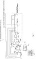
- Fig. 1 is a block diagram of a random number generation device 10 relating to this embodiment
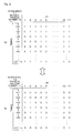
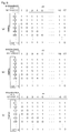
- Fig. 2 shows cyclic patterns of two M sequences generated by the random number generation device 10
- Fig. 3 is a block diagram of a physical random number generation section 14.
- the random number generation device 10 comprises a pseudo random number generation section 12, the physical random number generation section 14, and a switching section 16.
- the pseudo random number generation section 12, comprising at least one linear shift-register code generator can output random number patterns of a plurality of different pseudo random number sequences (for example, M sequences).
- a shift register 18 that includes a plurality of flip-flops connected in a cascaded arrangement, and an EXOR gate 20 that outputs the exclusive OR of output values from a predetermined plurality of tap positions, so as to form a linear shift-register code generator for outputting M sequence random numbers.
- a shift register 18 that includes a plurality of flip-flops connected in a cascaded arrangement, and an EXOR gate 20 that outputs the exclusive OR of output values from a predetermined plurality of tap positions, so as to form a linear shift-register code generator for outputting M sequence random numbers.
- the shift register 18 comprises 17 flip-flops configured as a 17-stage shift-register for shifting bits in response to a clock (CK), and on the basis of the tap outputs (Q outputs: Q3, Q17) from the 3 rd and 17 th flip-flops as counted from the input end, the feedback input value is generated (D1 input of shift register 18: "1" (high level) or "0" (low level)).
- the output of the EXOR gate 20 is directly fed back as an input to the shift register 18.
- the output of the EXOR gate 20 is input by the shift register 18 via the switching section 16.
- the switching section 16 switches between inverted and non-inverted output values from the EXOR 20 to become the feedback input value.
- the physical random output can be considered to be a switching control signal.
- the switching section 16 is formed by the EXOR gate. The EXOR gate outputs a "1" when the input values are different and a "0" when they are identical.
- the switching section 16 performs switching so that the output value of the EXOR gate 20 is inverted then fed back as the input value or directly fed back as the input value without being inverted.
- the operation of the switching section 16 enables the pseudo random number generation section 12 to generate two different pseudo random number sequences.
- an M sequence 1-1 (Fig. 2a) that cyclically varies in 2 17 -1 cycles on the basis of the clock signal (CK) is generated by the pseudo random number generation section 12.
- an M sequence 1-2 (Fig. 2b) that cyclically varies in 2 17 -1 cycles on the basis of the same clock signal is generated. It should be noted that the M sequence 1-1 and the M sequence 1-2 have the same changing pattern.
- the codes are inverted from each other, that they can be treated as different pseudo random number sequences.
- the switching signal that is supplied to the switching section 16 is controlled by physical random numbers, the use of intermediate information in the shift register generating one pseudo random number sequence to switch to another pseudo random number sequence yields a pseudo random number sequence that is impossible to predict.
- the frequency of the 0s and 1s in the two pseudo random number sequences has a symmetrical ratio of 2 16 -1 to 2 16 and 2 16 to 2 16 -1, respectively.
- controlling the switching of the two pseudo random number sequences on the basis of physical random numbers also has an effect of approximating an ideal frequency distribution of the 0s and 1s.
- the physical random number generation section 14 comprises a physical random number generation source 14a, an amplifier circuit 14b, and a binary converter circuit 14c.
- the physical random number generation source 14a generates signals that randomly change on the basis of natural phenomenon.
- a semiconductor device that generates noise signals, which are created in current paths including the junction can also be included.
- the decay of radioactive materials or other phenomenon may also be utilized as the physical random number generation source 14a.
- the signal generated at the physical random number generation source 14a is amplified at the amplifier circuit 14b, and undergoes binary conversion at the binary converter circuit 14c.
- the binary converter circuit 14c compares the amplitude of the amplified signal with a predetermined threshold value at a predetermined sampling timing. For example, when the amplitude of the amplified signal is higher than the predetermined threshold value, a "1" is output, and when it is lower, a "0" is output. In this manner, a physical random number output value having a predetermined voltage representing "1" or "0" is output from the physical random number generation section 14. It should be noted that although the threshold level in the binary converter circuit 14c can be arbitrarily set, it is normally set so that the probability of generation of 1s and 0s is substantially 1:1. It should also be noted that the output signal may also be generated simply by comparing the amplitude of the amplified signal with the predetermined threshold value at the binary converter circuit 14c.
- the random number generation device 10 not only switches the output between two different pseudo random number sequences according to physical random numbers but also changes the feedback state for the two pseudo random number sequences by effectively utilizing intermediate information in the shift register. This makes it more difficult to predict the random numbers compared to the case where pseudo random numbers only are used. Furthermore, since the physical random numbers are not directly used as the output random numbers, any adverse effect on the predictability of the output random numbers is substantially reduced compared with a conventional device even if the physical random number generating means are somehow manipulated from the outside.
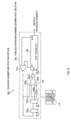
- Fig. 4 is a block diagram of a random number generation device 30 relating to this embodiment.
- the random number generation device 30 comprises a pseudo random number generation section 32, the physical random number generation section 14, and a switching section 36.
- the components that are identical to those in the above-mentioned embodiment are given the same reference numerals and their redundant descriptions are omitted here.
- the output value from the linear shift-register code generator is inverted or not inverted as an output random number by the switching section 36.
- a typical linear shift-register code generator is configured to include the shift register 18 and the EXOR gate 20. Outputs Q, a predetermined bit of the shift register 18 (for example, the 17 th bit), and Qb (inverted output of Q) are respectively input by the switching section 36.
- the switching section 36 comprises two AND gates 36a, 36b, of which one AND gate 36a inputs the Q output and the physical random number output from the physical random number generation section 14 via an inverter 36c, and the other AND gate 36b inputs the Qb output and the physical random number output from the physical random number generation section 14.
- the outputs of these two AND gates 36a, 36b are then input by an OR gate 36d and the output of the OR gate 36d becomes the output random number.
- the switching section 36 sets as valid one of either the Q output or the Qb output. Namely, when the physical random number output value is "1", the output value of the AND gate 36a is always “0” and the output value of the AND gate 36b becomes the same as the Qb output value so that the random number output value is the same as the Qb output value. Conversely, when the physical random number output value is "0", the output value of the AND gate 36b is always “0” and the output value of the AND gate 36a becomes the same as the Q output value so that the random number output value is the same as the Q output value.
- the random number generation device 30 relating to this embodiment can also switch and output the two random number sequences (M sequences 1-1, 1-2) shown in Fig. 2 according to the physical random number. Namely, an effect similar to that in embodiment 1 is also achieved by this configuration.
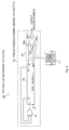
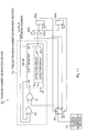
- Fig. 5 is a block diagram of a random number generation device 40 relating to this embodiment and Fig. 6 shows cyclic patterns of two M sequences generated by the random number generation device 40.
- the random number generation device 40 comprises a pseudo random number generation section 42, the physical random number generation section 14, and a switching section 46. It should be noted here also that the components that are identical to those in the above-mentioned embodiments are given the same reference numerals and their redundant descriptions are omitted.
- the pseudo random number generation section 42 relating to this embodiment can generate two types of feedback input values based on different combinations of taps in the linear shift-register code generator.
- the physical random number determines whether to pass or block the output of the EXOR gate 20b. More specifically, in the example of Fig. 5, the shift register 18 and multiple EXOR gates 20a, 20b, 20c for respectively outputting the exclusive OR of combinations of different tap outputs are provided as the linear shift-register code generator.
- the EXOR gate 20a outputs the exclusive OR of the 3 rd and 17 th tap outputs (Q3, Q17) as counted from the input side of the shift register 18, and the EXOR gate 20b outputs the exclusive OR of the 1 st and 2 nd tap outputs (Q1, Q2) as counted from the input side of the shift register 18.
- the output of the EXOR gate 20a is directly input by the EXOR gate 20c, whereas the output of the EXOR gate 20b is input by the EXOR gate 20c via the AND gate (switching section) 46.
- the AND gate 46 inputs the physical random number output from the physical random number generation section 14.
- the random number generation device 40 relating to this embodiment can also switch and output two random number sequences (M sequences 3-1, 3-2) according to the physical random number.
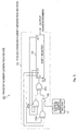
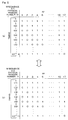
- Fig. 7 is a block diagram of a random number generation device 50 relating to this embodiment and Fig. 8 shows cyclic patterns of three M sequences generated by the random number generation device 50.
- the random number generation device 50 comprises a pseudo random number generation section 52, the physical random number generation section 14, and a switching section 56. It should be noted here that the components that are identical to those in the above-mentioned embodiments are given the same reference numerals and their redundant descriptions are omitted.
- the pseudo random number generation section 52 relating to this embodiment can generate three types of feedback input values based on different combinations of taps in the linear shift-register code generator.
- the physical random number determines which one of the three types of feedback input values is to be set as valid. More specifically, in the example of Fig. 7, the shift register 18 and multiple EXOR gates 20a, 20b, 20c, 20d for outputting the exclusive OR of input values based on combinations of different tap outputs are provided as the linear shift-register code generator.
- the EXOR gate 20a outputs the exclusive OR of the 3 rd and 17 th tap outputs (Q3, Q17) as counted from the input side of the shift register 18, the EXOR gate 20b outputs the exclusive OR of the 1 st and 2 nd tap outputs (Q1, Q2) as counted from the input side of the shift register 18, and the EXOR gate 20c outputs the exclusive OR of the 4 th and 7 th tap outputs (Q4, Q7) as counted from the input side of the shift register 18.
- the output of the EXOR gate 20a is directly input by the EXOR gate 20d, whereas the outputs of the EXOR gate 20b, 20c are input by the EXOR gate 20d via respective AND gates 56b, 56c, and an OR gate 56d.
- the AND gates 56b, 56c input the outputs from a 1/3 divider 56a.
- the 1/3 divider 56a, the AND gates 56b, 56c, and the OR gate 56d function as the switching section 56.
- the 1/3 divider 56a having a publicly known configuration, cyclically updates the output values Q1 and Q2 in three patterns, where the output values Q1 and Q2 are "0" and “0” for pattern 1, "1" and “0” for pattern 2, and "0" and “1” for pattern 3.
- the output value of the OR gate 56d becomes "0", in which case, the output value of the EXOR gate 20a is input by the shift register 18 as the feedback input value.
- the exclusive OR of the output value of the EXOR gate 20a and the output value of the EXOR gate 20c is output from the EXOR gate 20d as the feedback input value to the shift register 18.
- the pseudo random number generation section 52 are generated: [1] an M sequence 4-1 (Fig. 8a) where the feedback input value, based on the tap outputs of Q3 and Q17 that are input by the EXOR gate 20a, is valid; [2] an M sequence 4-2 (Fig. 8b) where the feedback input value, based on the tap outputs of Q1, Q2, Q3, and Q17 that are input by EXOR gates 20a, 20b, is valid; and [3] an M sequence 4-3 (Fig.
- the random number generation device 50 relating to this embodiment can switch and output the three random number sequences (M sequences 4-1, 4-2, 4-3) according to the physical random number.
- Fig. 9 is a block diagram of a random number generation device 60 relating to this embodiment and Fig. 10 shows cyclic patterns of two M sequences generated by the random number generation device 60.
- the random number generation device 60 comprises a pseudo random number generation section 62, the physical random number generation section 14, and a switching section 66. It should be noted here also that the components that are identical to those in the above-mentioned embodiments are given the same reference numerals and their redundant descriptions are omitted.
- the pseudo random number generation section 62 uses the same taps (from which the feedback input originates) for the feedback input and is configured so as to change the number of bits in the shift register, where the change in the number of bits in the shift register is determined by the physical random number. More specifically, in the example of Fig. 9, a 15-stage shift register 68, two flip-flops 62a, 62b disposed in a cascaded arrangement, and an EXOR gate 20e for outputting the exclusive OR of a combination of predetermined tap outputs are provided as the linear shift-register code generator.
- the EXOR gate 20e outputs the exclusive OR of the 1 st and 15 th tap outputs (Q1, Q15) as counted from the input side of the shift register 68.
- the output of the EXOR gate 20e is input by the flip-flop 62a at the front stage side and an AND gate 66a.
- the switching section 66 comprises two AND gates 66a, 66b.
- the AND gate 66a inputs the output of the EXOR gate 20e and the physical random number output from the physical random number generation section 14, and the AND gate 66b inputs a Q output and the physical random number output from the physical random number generation section 14 via an inverter 66c.
- the outputs of these two AND gates 66a, 66b are input by an OR gate 66d, and the output of the OR gate 66d is input by the shift register 68.
- the switching section 66 sets as valid one of either the output of the EXOR gate 20e or the output of the flip-flop 62b. Namely, when the physical random number output value is "0", the output value of the AND gate 66a is always "0" and the output value of the AND gate 66b becomes the same as the output value of the flip-flop 62b so that the output value of the OR gate 66d becomes the same as the output value of the flip-flop 62b.
- the output value of the AND gate 66b is always "0" and the output value of the AND gate 66a becomes the same as the output value of the EXOR gate 20e so that the output value of the OR gate 66d becomes the same as the output value of the EXOR gate 20e.
- the flip-flops 62a, 62b also function as part of the shift register.
- the 17-stage shift register including these flip-flops generates an M sequence 5-1 (Fig. 10a) where the feedback input value based on the tap outputs (Q3, Q17) is set as valid.
- the random number generation device 60 can switch and output random number sequences (M sequence 5-1, 5-2) generated by the two shift registers having a different number of stages according to the physical random number.
- Fig. 11 is a block diagram showing a random number generation device 70 relating to this embodiment.
- the random number generation device 70 comprises a pseudo random number generation section 72, the physical random number generation section 14, and the switching section 16.
- the pseudo random number generation section 72 of this embodiment is identical to the pseudo random number generation section 12 of embodiment 1, except that a detector circuit 78a (described hereinafter) is provided within a shift register 78 (18), and can generate the M sequences 1-1 and 1-2 shown in Fig. 2. It should be noted here also that the components that are identical to those in the above-mentioned embodiments are given the same reference numerals and their redundant descriptions are omitted.
- the linear shift-register code generator cannot generate M sequence codes depending on the code sequence within the shift register. For example, the M sequence 1-1 cannot be generated if all bit values of the shift register are "0" and the M sequence 1-2 cannot be generated if all bits of the shift register are "1".
- a conventional general linear shift-register code generator that generates only codes of one pseudo random number sequence was sufficient if care was taken in the initial value to avoid such a code sequence.
- it is preferable to design a countermeasure so that such a code sequence does not occur within the shift register with respect to a valid pseudo random number sequence.
- the random number generation device 70 relating to this embodiment also comprises, in addition to the random number generation device 10 relating to embodiment 1, detector circuits 78a, 78b, AND gates 82a, 82b, flip-flops 84a, 84b, and a flip-flop 80.
- the output (physical random number output) from the physical random number generation section 14 is input by the flip-flop 80.
- This embodiment also provides that the physical random number output value "0" indicates the M sequence 1-1 (Fig. 2a) and "1" indicates the M sequence 1-2 (Fig. 2b).
- the detector circuit 78a When all bit values of the shift register 78 are "1”, the detector circuit 78a outputs "1" (for example, outputs the AND of all bit values) to the AND gate 82a.
- the detector circuit 78b outputs "1" to the AND gate 82b (for example, outputs the AND of the inverted values of all bits).
- the AND gate 82a inputs the output of the detector circuit 78a and the Q output of the flip-flop 80, and the output of the AND gate 82a is input by the flip-flop 84a.
- the AND gate 82b inputs the output of the detector circuit 78b and the Qb output of the flip-flop 80, and the output of the AND gate 82b is input by the flip-flop 84b.
- the flip-flop 80 inputs the output of the flip-flop 84a as a reset signal (R input) and the output of the flip-flop 84b as a set signal (S input).
- R input reset signal
- S input set signal
- the value of at least one bit of the shift register 78 is changed by the outputs of the flip-flops 84a, 84b.
- the value of that flip-flop (bit) becomes "0" so that it is possible to prevent the state where the codes for the M sequence 1-1 are not generated.
- the output of the flip-flop 84b is used as the reset signal for any internal flip-flop forming the shift register 78, the value of that flip-flop (bit) becomes "1" so that it is possible to prevent the state where the codes for the M sequence 1-2 are not generated.
- the output from the flip-flop at the final stage of the shift register as the random number output
- the output from another flip-flop may be used as the random number output or the feedback value that is input by the shift register may be used as the random number output.
- random numbers having a higher degree of safety can be generated, such as in an application to an encryption algorithm where the prediction of random numbers is difficult, since one of a plurality of pseudo random number sequences is set as valid as a result of the physical random number based switching.
- the present invention is suited for use in applications, such as encryption technology, where a higher degree of safety is required.
Landscapes
- Engineering & Computer Science (AREA)
- Physics & Mathematics (AREA)
- Theoretical Computer Science (AREA)
- General Physics & Mathematics (AREA)
- Mathematical Optimization (AREA)
- Computational Mathematics (AREA)
- Signal Processing (AREA)
- Mathematical Analysis (AREA)
- Computer Networks & Wireless Communication (AREA)
- Pure & Applied Mathematics (AREA)
- General Engineering & Computer Science (AREA)
- Computer Security & Cryptography (AREA)
- Tests Of Electronic Circuits (AREA)
- Detection And Prevention Of Errors In Transmission (AREA)
- Test And Diagnosis Of Digital Computers (AREA)
- Pinball Game Machines (AREA)
- Logic Circuits (AREA)
Applications Claiming Priority (3)
| Application Number | Priority Date | Filing Date | Title |
|---|---|---|---|
| JP2002320035 | 2002-11-01 | ||
| JP2002320035A JP2004157168A (ja) | 2002-11-01 | 2002-11-01 | 乱数生成装置 |
| PCT/JP2003/014055 WO2004040838A1 (ja) | 2002-11-01 | 2003-11-04 | 乱数生成装置 |
Publications (1)
| Publication Number | Publication Date |
|---|---|
| EP1564927A1 true EP1564927A1 (de) | 2005-08-17 |
Family
ID=32211834
Family Applications (1)
| Application Number | Title | Priority Date | Filing Date |
|---|---|---|---|
| EP03770125A Withdrawn EP1564927A1 (de) | 2002-11-01 | 2003-11-04 | Zufallszahlengenerator |
Country Status (5)
| Country | Link |
|---|---|
| US (1) | US20060123072A1 (de) |
| EP (1) | EP1564927A1 (de) |
| JP (1) | JP2004157168A (de) |
| TW (1) | TWI240201B (de) |
| WO (1) | WO2004040838A1 (de) |
Families Citing this family (6)
| Publication number | Priority date | Publication date | Assignee | Title |
|---|---|---|---|---|
| JP4533721B2 (ja) * | 2004-10-21 | 2010-09-01 | 株式会社大都技研 | 遊技台 |
| TW200629192A (en) * | 2005-02-03 | 2006-08-16 | Sanyo Electric Co | Random number generating circuit |
| KR101870249B1 (ko) * | 2012-01-25 | 2018-06-22 | 삼성전자주식회사 | 디더 제어 회로와 이를 포함하는 장치들 |
| US11757632B2 (en) * | 2018-12-19 | 2023-09-12 | Micron Technology, Inc. | Generating a random value based on a noise characteristic of a memory cell |
| US11586418B2 (en) * | 2020-01-17 | 2023-02-21 | Macronix International Co., Ltd. | Random number generator, random number generating circuit, and random number generating method |
| GB2601171B (en) | 2020-11-20 | 2023-05-24 | Toshiba Kk | System and method to generate biased random bit streams and quantum communication system and method |
Family Cites Families (9)
| Publication number | Priority date | Publication date | Assignee | Title |
|---|---|---|---|---|
| JPS6025611Y2 (ja) * | 1980-04-21 | 1985-08-01 | ニコ−電子株式会社 | 乱数発生回路 |
| US4852023A (en) * | 1987-05-12 | 1989-07-25 | Communications Satellite Corporation | Nonlinear random sequence generators |
| US5297207A (en) * | 1993-05-24 | 1994-03-22 | Degele Steven T | Machine generation of cryptographic keys by non-linear processes similar to processes normally associated with encryption of data |
| US5365585A (en) * | 1993-08-30 | 1994-11-15 | Motorola, Inc. | Method and apparatus for encryption having a feedback register with selectable taps |
| WO1995015633A1 (en) * | 1993-12-01 | 1995-06-08 | William Michael Raike | A non-deterministic public key encryption system |
| US6324558B1 (en) * | 1995-02-14 | 2001-11-27 | Scott A. Wilber | Random number generator and generation method |
| JP3277139B2 (ja) * | 1997-03-13 | 2002-04-22 | インターナショナル・ビジネス・マシーンズ・コーポレーション | 入力ビット列暗号化装置及び方法 |
| US6253223B1 (en) * | 1999-06-08 | 2001-06-26 | General Instrument Corporation | Robust random number generator |
| US7028059B2 (en) * | 2002-06-24 | 2006-04-11 | Sun Microsystems, Inc. | Apparatus and method for random number generation |
-
2002
- 2002-11-01 JP JP2002320035A patent/JP2004157168A/ja active Pending
-
2003
- 2003-10-31 TW TW092130446A patent/TWI240201B/zh active
- 2003-11-04 WO PCT/JP2003/014055 patent/WO2004040838A1/ja not_active Ceased
- 2003-11-04 US US10/533,256 patent/US20060123072A1/en not_active Abandoned
- 2003-11-04 EP EP03770125A patent/EP1564927A1/de not_active Withdrawn
Non-Patent Citations (1)
| Title |
|---|
| See references of WO2004040838A1 * |
Also Published As
| Publication number | Publication date |
|---|---|
| WO2004040838A1 (ja) | 2004-05-13 |
| US20060123072A1 (en) | 2006-06-08 |
| JP2004157168A (ja) | 2004-06-03 |
| TW200421170A (en) | 2004-10-16 |
| TWI240201B (en) | 2005-09-21 |
Similar Documents
| Publication | Publication Date | Title |
|---|---|---|
| US7424500B2 (en) | Random number generator with ring oscillation circuit | |
| JP3696209B2 (ja) | シード生成回路、乱数生成回路、半導体集積回路、icカード及び情報端末機器 | |
| JPH0682528A (ja) | 制御可能な重み付き2進シーケンスを発生するための回路 | |
| JPH02128218A (ja) | 乱数発生器 | |
| KR20140108362A (ko) | 난수 발생기 | |
| US20130346459A1 (en) | Method for generating random numbers | |
| US9465585B2 (en) | Method for detecting a correlation | |
| Fujieda | On the feasibility of TERO-based true random number generator on Xilinx FPGAs | |
| JP4288057B2 (ja) | 乱数生成装置 | |
| US8081017B2 (en) | Clock signal frequency dividing circuit and clock signal frequency dividing method | |
| EP1564927A1 (de) | Zufallszahlengenerator | |
| CN103514080B (zh) | 用于监控随机发生器的输出的方法 | |
| JP4417389B2 (ja) | デジタルロジックを利用した乱数発生装置及び方法 | |
| US9116764B2 (en) | Balanced pseudo-random binary sequence generator | |
| US9720650B2 (en) | Method for post-processing an output of a random source of a random generator | |
| CN109558111B (zh) | 基于d触发器亚稳态特性的真随机数生成装置 | |
| Sarkar et al. | The set of reversible 90150 cellular automata is regular | |
| CN1720501A (zh) | 用于纯随机数发生器的系统和方法 | |
| Mihaljev'c | Security examination of a cellular automata based pseudorandom bit generator using an algebraic replica approach | |
| KR100735953B1 (ko) | 일련 번호 생성 장치, 그 방법 및 컴퓨터 판독가능 저장매체 | |
| US7502814B2 (en) | Device and method for generating a pseudorandom sequence of numbers | |
| Sekhar et al. | An Efficient Pseudo Random Number Generator for Cryptographic Applications | |
| US20150019603A1 (en) | Method for checking an output of a random number generator | |
| JP2792242B2 (ja) | 反転回路付きスクランブラ | |
| JP3350076B2 (ja) | ジョンソン・カウンタの誤動作回避回路 |
Legal Events
| Date | Code | Title | Description |
|---|---|---|---|
| PUAI | Public reference made under article 153(3) epc to a published international application that has entered the european phase |
Free format text: ORIGINAL CODE: 0009012 |
|
| 17P | Request for examination filed |
Effective date: 20050530 |
|
| AK | Designated contracting states |
Kind code of ref document: A1 Designated state(s): AT BE BG CH CY CZ DE DK EE ES FI FR GB GR HU IE IT LI LU MC NL PT RO SE SI SK TR |
|
| RBV | Designated contracting states (corrected) |
Designated state(s): DE FR GB IT NL |
|
| RIN1 | Information on inventor provided before grant (corrected) |
Inventor name: TAMAKI, HARUO., Inventor name: IKETANI, AKIRA,C/O SANYO SEMICON DEVICE CO., LTD. Inventor name: ONAYA, MASATO,C/O SANYO ELECTRIC CO., LTD. |
|
| STAA | Information on the status of an ep patent application or granted ep patent |
Free format text: STATUS: THE APPLICATION HAS BEEN WITHDRAWN |
|
| 18W | Application withdrawn |
Effective date: 20090213 |