EP1564889B1 - Zentrieren eines Spannungsgesteuerten Mehrbandoszillators - Google Patents
Zentrieren eines Spannungsgesteuerten Mehrbandoszillators Download PDFInfo
- Publication number
- EP1564889B1 EP1564889B1 EP04019807A EP04019807A EP1564889B1 EP 1564889 B1 EP1564889 B1 EP 1564889B1 EP 04019807 A EP04019807 A EP 04019807A EP 04019807 A EP04019807 A EP 04019807A EP 1564889 B1 EP1564889 B1 EP 1564889B1
- Authority
- EP
- European Patent Office
- Prior art keywords
- vco
- signal
- frequency
- band
- counter
- Prior art date
- Legal status (The legal status is an assumption and is not a legal conclusion. Google has not performed a legal analysis and makes no representation as to the accuracy of the status listed.)
- Expired - Lifetime
Links
- 230000008859 change Effects 0.000 claims description 35
- 238000000034 method Methods 0.000 claims description 28
- 230000004044 response Effects 0.000 claims description 12
- 230000008569 process Effects 0.000 description 14
- 238000005259 measurement Methods 0.000 description 8
- 230000007423 decrease Effects 0.000 description 4
- 230000003247 decreasing effect Effects 0.000 description 2
- 238000010586 diagram Methods 0.000 description 2
- 238000009738 saturating Methods 0.000 description 2
- 230000035945 sensitivity Effects 0.000 description 2
- 230000007704 transition Effects 0.000 description 2
- 230000032683 aging Effects 0.000 description 1
- 238000001514 detection method Methods 0.000 description 1
- 230000009977 dual effect Effects 0.000 description 1
- 230000000694 effects Effects 0.000 description 1
- 238000005516 engineering process Methods 0.000 description 1
- 230000007613 environmental effect Effects 0.000 description 1
- 230000007246 mechanism Effects 0.000 description 1
- 229910044991 metal oxide Inorganic materials 0.000 description 1
- 150000004706 metal oxides Chemical class 0.000 description 1
- 229920000729 poly(L-lysine) polymer Polymers 0.000 description 1
- 230000000979 retarding effect Effects 0.000 description 1
- 230000000630 rising effect Effects 0.000 description 1
- 238000005096 rolling process Methods 0.000 description 1
- 239000004065 semiconductor Substances 0.000 description 1
Images



Classifications
-
- H—ELECTRICITY
- H03—ELECTRONIC CIRCUITRY
- H03L—AUTOMATIC CONTROL, STARTING, SYNCHRONISATION OR STABILISATION OF GENERATORS OF ELECTRONIC OSCILLATIONS OR PULSES
- H03L7/00—Automatic control of frequency or phase; Synchronisation
- H03L7/06—Automatic control of frequency or phase; Synchronisation using a reference signal applied to a frequency- or phase-locked loop
- H03L7/08—Details of the phase-locked loop
- H03L7/085—Details of the phase-locked loop concerning mainly the frequency- or phase-detection arrangement including the filtering or amplification of its output signal
- H03L7/095—Details of the phase-locked loop concerning mainly the frequency- or phase-detection arrangement including the filtering or amplification of its output signal using a lock detector
-
- H—ELECTRICITY
- H03—ELECTRONIC CIRCUITRY
- H03L—AUTOMATIC CONTROL, STARTING, SYNCHRONISATION OR STABILISATION OF GENERATORS OF ELECTRONIC OSCILLATIONS OR PULSES
- H03L7/00—Automatic control of frequency or phase; Synchronisation
- H03L7/06—Automatic control of frequency or phase; Synchronisation using a reference signal applied to a frequency- or phase-locked loop
- H03L7/08—Details of the phase-locked loop
- H03L7/085—Details of the phase-locked loop concerning mainly the frequency- or phase-detection arrangement including the filtering or amplification of its output signal
- H03L7/087—Details of the phase-locked loop concerning mainly the frequency- or phase-detection arrangement including the filtering or amplification of its output signal using at least two phase detectors or a frequency and phase detector in the loop
-
- H—ELECTRICITY
- H03—ELECTRONIC CIRCUITRY
- H03L—AUTOMATIC CONTROL, STARTING, SYNCHRONISATION OR STABILISATION OF GENERATORS OF ELECTRONIC OSCILLATIONS OR PULSES
- H03L7/00—Automatic control of frequency or phase; Synchronisation
- H03L7/06—Automatic control of frequency or phase; Synchronisation using a reference signal applied to a frequency- or phase-locked loop
- H03L7/08—Details of the phase-locked loop
- H03L7/10—Details of the phase-locked loop for assuring initial synchronisation or for broadening the capture range
- H03L7/113—Details of the phase-locked loop for assuring initial synchronisation or for broadening the capture range using frequency discriminator
Definitions
- the invention relates to phase-locked loops, and more particularly, to determining the correct frequency band for centering a multi-band voltage controlled oscillator in a phase-locked loop.
- Monolithically integrated clock and data recover (CDR) circuits often use ring oscillators as voltage controlled oscillators (VCOs).
- VCOs voltage controlled oscillators
- CMOS complimentary metal oxide semiconductor
- PLL phase-locked loop
- Providing a wide tuning range typically requires a large tuning gain over a limited tuning voltage range.
- the larger the tuning gain the more sensitive the VCO is to noise on the tuning signal. Sensitivity to noise can be a major problem in an integrated circuit that has several CDR channels or a large digital section in addition to the CDR.
- Multi-band VCOs One technique that is used to reduce the magnitude of the required tuning gain and to reduce the corresponding noise sensitivity while still providing a wide frequency range involves splitting the entire frequency tuning range of a VCO into multiple overlapping frequency bands. VCOs that are configured with multiple overlapping frequency bands are generally referred to as "multi-band VCOs.” Controlling multi-band VCOs to lock onto the setpoint frequency of the VCO is a two step process. The first step involves "centering" the VCO by selecting a frequency band that includes the setpoint frequency. In most multi-band VCO implementations, the frequency bands overlap each other at their boundaries and therefore centering involves selecting the frequency band with the center frequency that is nearest to the setpoint frequency.
- the second step involves adjusting the analog phase-locked loop (PLL) control voltage to drive the VCO to phase and frequency lock.
- PLL phase-locked loop
- a technique for centering a multi-band VCO involves comparing a VCO tuning signal to a pre-established tuning signal window to determine whether to change the frequency band of the multi-band VCO.
- the frequency band of the multi-band VCO can be changed only when the tuning signal is outside the tuning signal window. Centering a multi-band VCO in response to a comparison of the VCO tuning signal to a tuning signal window enables the centering process to function on a continuous basis while the phase-locked loop is in normal operation and without having to go through a restart process.
- the frequency band of a VCO can be changed in the centering process as long as the VCO is being controlled by a frequency detector.
- the multi-band VCO achieves lock, the multi-band VCO is changed by at least one more frequency band as long as the VCO tuning signal is still outside the tuning signal window. Changing the multi-band VCO by at least one more frequency band after the multi-band VCO achieves lock and as long as the tuning signal is outside the tuning signal window ensures that the multi-band VCO is centered at a frequency band that will allow frequency adjustments to account for frequency drift while using a tuning signal that is within the tuning signal window.
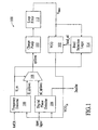
- Fig. 1 depicts a PLL that includes band selection logic that is responsive to a control signal from a frequency detector and a VCO tuning signal from a loop filter.
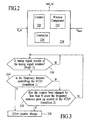
- Fig. 2 depicts an expanded view of the band selection logic from Fig. 1 that includes a counter, a window comparator, and a controller.
- Fig. 3 depicts an example of the logic involved in determining whether or not a counter is allowed to change, thereby changing a band select signal that controls the centering of a multi-band VCO.
- Fig. 4 depicts an embodiment of the band selection logic depicted in Fig. 2.
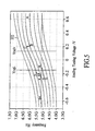
- Fig. 5 depicts an exemplary VCO frequency trajectory during a VCO centering operation using the band selection logic described with reference to Figs. 1 - 4.
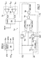
- Fig. 6 depicts a frequency detector that is similar to the frequency detector of Fig. 1 except that it includes additional "gate” and “control” signals.
- Fig. 7 depicts another embodiment of the band selection logic depicted in Fig. 2.
- Fig. 8 depicts an exemplary VCO frequency trajectory during a VCO centering operation using the band selection logic described with reference to Figs. 1, 3, 6, and 7.
- Fig. 9 depicts exemplary waveforms related to operation of the controller of Fig. 7.
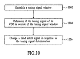
- Fig. 10 is a process flow diagram of a method for centering a multi-band VCO.
- the task of a PLL is to lock the phase and frequency of a VCO signal to a particular signal, referred to herein as an input signal.
- PLLs with multi-band VCOs should be switched to a frequency band with a center frequency that is near the setpoint frequency of the VCO.
- centering a multi-band VCO involves comparing a VCO tuning signal to a pre-established tuning signal window to determine whether or not to change the frequency band of the multi-band VCO.
- Fig. 1 depicts an embodiment of a PLL 100 that includes a voltage controlled oscillator (VCO) 102, a digital phase detector 104, a frequency detector 106, a multiplexer 108, a charge pump 110, a loop filter 112, and band selection logic 114.
- the digital phase detector 104 is connected to receive an input signal from a signal source and a portion of the VCO signal (VCO in ) from the VCO.
- the input signal carries clock information and data that is to be recovered.
- the digital phase detector compares transitions of the input signal with transitions of the VCO signal and generates an output (referred to herein as the "pd_up/down" signal) that indicates the phase difference between the input signal and the VCO signal.
- the digital phase detector produces an "up” signal when the phase of the input signal leads the phase of the VCO signal and a “down” signal when the phase of the input signal lags the phase of the VCO signal.
- An up signal is used to drive the frequency of the VCO upward while a down signal is used to drive the frequency of the VCO signal downward, thereby advancing or retarding, respectively, the phase of the VCO signal.
- the digital phase detector also outputs the recovered data (DataOut). This data is not critical to the invention and is not described further.
- the frequency detector 106 is connected to receive a portion of the VCO signal (VCO in ) from the VCO 102 and a reference clock signal (RefClk) from a reference clock source (often external to the system and not shown here).
- the frequency detector uses the reference clock signal to determine whether or not the VCO signal should be controlled by the frequency detector.
- the frequency detector controls the VCO when the frequency of the VCO signal is outside a pre-established deadband region that is centered at a setpoint frequency of the VCO.
- the frequency detector generates a control signal (referred to herein as the "fd_en” signal) that indicates whether the VCO is to be controlled by the frequency detector or the digital phase detector 104 (that is, whether control of the VCO by the frequency detector is enabled or disabled).
- the frequency detector When the frequency detector does not control the VCO because the frequency of the VCO is within the deadband region, the system is said to be in "lock.” When the frequency detector does control the VCO because the frequency of the VCO is outside the deadband region, the system is said to be out of lock.
- the frequency detector also generates an output (referred to herein as the "fd_up/down" signal) that indicates the sign of the frequency difference between the frequency of the VCO signal and the setpoint frequency.
- the control signal (fd_en) when the control signal (fd_en) is high (e.g., fd_en is "high"), the output (fd_up/down) from the frequency detector controls the VCO.
- the output (pd_up/down) from the digital phase detector controls the VCO.
- the portion of the VCO signal that is received at the frequency detector and the digital phase detector may be divided by N using a signal divider (not shown).
- the function of the frequency detector can be performed by a more general "lock detector,” which determines whether control of the VCO should be given up to the digital phase detector.
- the lock detector may use other criteria, such as bit errors or consistency of phase, to determine if/when control of the VCO should be given up to the digital phase detector. Even if lock detection is not based on a frequency measurement, there is still a need for a frequency detector that generates a signal representing the sign of the frequency difference between the VCO signal and a reference signal.
- the multiplexer 108 receives the control signal (fd_en) from the frequency detector 106 and allows the corresponding control signal (either fd_up/down from the frequency detector or pd_up/down from the digital phase detector 104) to control the charge pump 110.
- the charge pump receives an "up/down” signal from the multiplexer and transfers a positive charging current to the loop filter if the up/down signal is "up” or a negative charging current if the up/down signal is "down.”
- the loop filter 112 generates a VCO tuning signal (referred to in the figures as V tune ) in response to an output from the charge pump.
- the tuning voltage output from the loop filter is increased, thereby causing the frequency of the VCO 102 to increase. Conversely, when a negative charging current is received from the charge pump, the tuning voltage output from the loop filter is decreased, thereby causing the frequency of the VCO to decrease.
- the band selection logic 114 is connected to receive the control signal (fd_en) from the frequency detector 106 and the VCO tuning signal (V tune ) from the loop filter 112.
- the band selection logic outputs a band selection signal (referred to in the figures as the "band_sel" signal) in response to the control signal (fd_en) and the VCO tuning signal (V tune ).
- the band selection signal determines the frequency band in which the multi-band VCO 102 is to operate.
- the band selection logic is described in more detail below with regard to Figs. 2 - 10.
- Operation of the PLL 100 depicted in Fig. 1 involves tuning the VCO 102 in response to continuous feedback from the digital phase detector 104, the frequency detector 106, and the band selection logic 114.
- the VCO receives the VCO tuning signal (V tune ) from the loop filter 112 and produces a VCO signal as an output.
- a portion of the VCO signal (VCO in ) is fed into the digital phase detector and the frequency detector.
- the digital phase detector and the frequency detector generate output signals (pd_up/down, fd_en, and fd_up/down) in response to the VCO signal (VCO in ).
- the output signal from one of the digital phase detector and the frequency detector selected by the multiplexer 108 in response to the control signal (fd_en) is used to continually adjust the VCO control signal (V tune ) and as a result the frequency of the VCO.
- the band selection logic controls the frequency band in which the VCO operates in response to the control signal (fd_en) from the frequency detector and the VCO tuning signal (V tune ) from the loop filter.
- Fig. 2 depicts an embodiment of band selection logic that includes a counter 220, a window comparator 222, and a controller 224.
- the band selection logic receives the VCO tuning signal (V tune ) from the loop filter 112 (Fig. 1) and the control signal (fd_en) from the frequency detector 106 (Fig. 1) and in response outputs a band selection signal (band_sel).
- the counter is a digital counter whose counter value corresponds to a frequency band of the VCO.
- a 3-bit binary counter can be used to individually identify (e.g., via the band_sel signal) each band of a multi-band VCO that has eight frequency bands.
- the counter can be a saturating up/down counter. The saturating up/down counter does not roll over when it reaches all zeroes or all ones.
- the counter, and, hence, the band is allowed to change only when two requirements are met.
- the first requirement is met when the VCO tuning signal (V tune ) is outside a pre-established tuning signal window. Whether the first requirement is met is determined by the window comparator.
- the second requirement is met when one of two conditions is satisfied.
- the second requirement is met when the frequency detector is controlling the VCO.
- the second requirement is met when fd_en is high.
- the second requirement is met when the counter has changed by less than a predefined number, N, after the frequency detector gives up control of the VCO.
- N a predefined number
- the counter is allowed to change by one (i.e., either to increase or decrease by one) after the frequency detector has given up control of the VCO provided that the first requirement is also met (i.e., the VCO tuning signal (V tune ) is outside the tuning signal window).
- the controller is incremented when the VCO tuning signal (V tune ) is above an upper boundary of the tuning signal window and is decremented when the VCO tuning signal (V tune ) is below a lower boundary of the tuning signal window.
- Fig. 3 depicts an example of the logic involved in determining whether the counter is allowed to change, thereby changing the band select signal that controls the centering of the multi-band VCO.
- decision point 330 it is determined whether the VCO tuning signal (V tune ) is outside the tuning signal window. If the VCO tuning signal (V tune ) is not outside the tuning signal window, then no counter change is allowed and the process returns to the beginning. If the VCO tuning signal (V tune ) is outside the tuning signal window, then the process moves to decision point 334.
- decision point 334 it is determined whether or not the frequency detector is controlling the VCO. If the frequency detector is controlling the VCO, then a counter change is allowed (either by incrementing or decrementing) as indicated by the result block 336.
- decision point 334 it is determined that the frequency detector is not controlling the VCO, then the process moves to decision point 338.
- decision point 338 it is determined whether the counter has been changed less than N times since the frequency detector gave up control of the VCO. If the answer is no "N” (the counter has been changed N or more times), then the counter cannot be changed at this time and the process returns to the beginning. If the answer is yes "Y" (the counter has been changed less than N times), then a counter change is allowed as indicated by result block 336.
- Fig. 4 depicts details of an embodiment of the band selection logic 214 depicted in Fig. 2.
- the band selection logic 414 depicted in Fig. 4 includes a counter 420, a window comparator 422, and a controller 424.
- the window comparator is implemented using two voltage comparators 444 with each of the two voltage comparators having an input that receives the VCO tuning voltage and an input that receives a boundary voltage.
- the voltage comparators compare the VCO tuning signal (V tune ) to the two voltages that make up the boundaries of the tuning voltage window and provide outputs (referred to herein as "cmp_up" and "cmp_dn”) that indicate if either of the voltage boundaries have been exceeded.
- the upper voltage boundary of the tuning signal window is referred to as V ref+ and the lower voltage boundary of the tuning signal window is referred to as V ref- .
- V ref+ the upper voltage boundary of the tuning signal window
- V ref- the lower voltage boundary of the tuning signal window
- boundary voltages of the tuning signal window are pre-established as a fraction of the analog tuning signal range of the VCO, such that there is enough tuning range left between either end of the tuning signal window and the ends of the analog tuning signal range to allow for the worst-case expected drift of the VCO due to temperature and supply variations as well as device aging. Assuming a constant input frequency, such VCO drift requires adjustment of the tuning signal to maintain lock. The required adjustment of the VCO tuning signal should not reach the limits of the tuning signal range or the tuning will fail and the PLL will lose lock. If the input frequency is expected to drift over time, an increased margin between the ends of the tuning signal window and the ends of the analog tuning signal range may be necessary to maintain lock without triggering a new centering cycle.
- V ref+ and V ref- can be set, for example, using a digital-to-analog converter (DAC) or by a resistor string.
- DAC digital-to-analog converter
- the controller 424 is implemented using a D flip-flop (DFF) 446, an OR gate 448, and two AND gates 450.
- the DFF receives inputs from an external clock (referred to herein as "slowClk”) and from the frequency detector (fd_en).
- the clock signal (slowClk) is also connected to the counter 420.
- the OR gate receives an input from the DFF and from the frequency detector (fd_en) and outputs a control signal (referred to herein as update_counter) if either one of the received signals is high.
- the DFF and the OR gate "stretch" the control signal (fd_en) from the frequency detector such that the control signal (update_counter) is high whenever the control signal (fd_en) is high and remains high for one more period of the clock signal (slowClk) after the control signal (fd_en) goes low.
- the resulting signal (update_counter) from the OR gate is fed into each of the AND gates along with the results from the comparator.
- the AND gates gate the comparator output signals, passing the outputs of the comparator to the counter control signals (referred to herein as "cnt_up” and “cnt_dn”) only if the control signal (update_counter) from the OR gate is high.
- the counter 420 is incremented or decremented by one count (depending on whether cmp_up or cmp_dn is high) for each rising edge of the clock signal (slowClk) as long as the VCO tuning signal (V tune ) is outside the tuning signal window.
- the counter keeps its state when neither cnt_up nor cnt_dn are high.
- the counter also "saturates" (i.e., keeps its state instead of rolling over) when the counter is in an all ones state and cnt_up is high or when the counter is in an all zeroes state and cnt_dn is high.
- Fig. 5 depicts an exemplary VCO frequency trajectory during a VCO centering operation using the band selection logic described with reference to Figs. 2 - 4.
- Fig. 5 depicts eight exemplary VCO tuning curves 552 of VCO frequency on the vertical axis and analog tuning voltage on the horizontal axis.
- the VCO tuning curves correspond to eight selectable frequency bands (e.g., for any analog tuning voltage on the horizontal axis there are eight possible values of the VCO frequency depending on which frequency band is selected).
- the two vertical lines marked V ref+ and V ref- identify the voltage boundaries of the tuning signal window.
- the horizontal line marked " f set " identifies the setpoint frequency of the PLL.
- the dark arrows identify the exemplary centering trajectory of the VCO frequency that results from the band selection logic 414 depicted in Fig. 4.
- the frequency detector drives the tuning voltage more negative (to the left in Fig. 5).
- the frequency detector drives the tuning voltage more positive (to the right in Fig. 5).
- the frequency detector gives up control of the VCO to the digital phase detector, which then drives the VCO towards phase lock.
- the counter is clocked (e.g., if a positive edge of the slowClk signal arrives) while the tuning voltage is above V ref+ , then the counter is allowed to change the VCO by one frequency band to a higher frequency band.
- the counter is clocked while the tuning voltage is below V ref- , then the counter is allowed to change the VCO by one frequency band to a lower frequency band.
- the counter is clocked at regular time intervals. In the example of Fig. 5, the intervals are spaced such that, under control of the frequency detector, the tuning voltage changes by approximately 0.4V between clock events.
- the update_counter signal is allowed to go high one more time, which allows one more counter change if the VCO tuning signal is outside the tuning signal window.
- the counter does not roll over but saturates at each end of its counting range (e.g., all zeroes or all ones).
- the VCO frequency is above the setpoint frequency ( f set ) and therefore the VCO tuning signal is driven lower by the frequency detector, thereby driving the VCO frequency lower along path A-B.
- the counter is clocked. Because the VCO tuning signal is outside the tuning signal window (greater than V ref+ ) and the frequency detector is controlling the VCO, the counter is incremented by one, which causes the VCO frequency to shift up one frequency band to point C.
- the VCO frequency is still above the setpoint frequency ( f set ) and therefore the frequency detector drives the VCO tuning signal lower, which drives the VCO frequency lower along path C-D.
- the counter will not change because the VCO tuning signal is within the tuning signal window. In this example, the tuning voltage is driven all the way across the tuning signal window between updates.
- the counter is clocked again. Because the VCO tuning signal is outside the tuning signal window (e.g., less than V ref- ) and the frequency detector is still controlling the VCO, the counter is decremented by one, which causes the VCO to shift down by one frequency band to point E.
- the frequency detector drives the VCO tuning signal lower, which drives the VCO frequency lower along path E-F.
- the PLL achieves frequency lock and the frequency detector gives up control of the VCO to the digital phase detector.
- the counter is clocked again, because the VCO tuning signal is still outside the tuning signal window (less than V ref- ) and the update_counter signal remains high, the counter is decremented one more time (e.g., by one count) even though the frequency detector no longer controls the VCO.
- the counter change causes the VCO frequency to shift down by one frequency band to point G.
- the shift in frequency bands causes the PLL to lose lock and control of the VCO reverts to the frequency detector. Because the VCO frequency is below the setpoint frequency ( f set ), the frequency detector drives VCO tuning signal higher, which drives the VCO frequency higher along path G-H.
- the PLL again achieves frequency lock and the frequency detector gives up control of the VCO to the digital phase detector.
- the update_counter signal remains high but because the VCO tuning signal is within the tuning signal window, the counter is not allowed to change. Further clock edges have no effect on the counter because the update_counter signal remains low as long as the PLL is in lock.
- the VCO tuning signal (V tune ) is outside the tuning signal window (less than V ref- ) and the counter is allowed to change one more time (e.g., by one count) at the next clock event.
- the additional count change throws the PLL out of lock.
- the frequency detector regains control of the VCO and drives the PLL to a new lock point inside the tuning signal window (e.g., at point H). With the VCO tuning signal within the tuning signal window, the counter is prevented from reacting to clock events and the PLL stays in this stable point.
- the additional counter change after the initial phase lock acquisition is crucial to finding a stable point inside the tuning signal window.
- Selecting a frequency band using the above-described technique allows a margin of error to account for frequency drift that may occur during operation. If the supply voltage or the operating temperature change after the end of the centering sequence, the VCO tuning curves may shift up or down as well as change shape to some degree and the PLL will change the tuning voltage (V tune ) in order to maintain phase lock. The resulting frequency drift may move the tuning voltage out of the tuning signal window but will not cause re-centering since the frequency detector will not regain control during gradual changes.
- the PLL will lose lock, the frequency detector will regain control, and the centering sequence will be performed to move the PLL back towards the center of the tuning signal window. That is, the continuous nature of the band selection logic operation prevents the PLL from failing and will cause the multi-band VCO to automatically re-center if frequency drift causes the VCO tuning signal to limit out.
- the corresponding comparator may not have a well defined logic level output signal. This is referred to as being in a "metastable" state. This indeterminate state may propagate into the counter and may cause the counter state to change in a random way instead of up or down by exactly one count. In the example centering trajectory of Fig. 5, such an event would constitute a vertical jump of the trajectory to some random tuning curve. From the random tuning curve, the system finds its way back to phase lock within the tuning signal window according to the band selection logic described above with no negative consequences other than a somewhat longer time to completion of the centering sequence.
- the frequency detector 106 depicted in Fig. 1 includes functionality and outputs that are used by an embodiment 714 of the band selection logic 114 in the band selection process.
- Fig. 6 depicts a frequency detector 606 that is similar to the frequency detector of Fig. 1 except that it provides additional "gate” and "preset” signals.
- the gate signal is used to start and stop a counter that is internal to the frequency detector, and which is used by the frequency detector for frequency measurements.
- the preset signal is used to set the frequency detector's internal counter to a pre-established preset value as part of the frequency measurement process.
- Fig. 7 depicts details of embodiment 714 of the band selection logic 214 depicted in Fig. 2.
- the band selection logic 714 of Fig. 7 includes a counter 720, a window comparator 722, and a controller 724.
- the counter clock signal (update_counter) is applied directly to the counter 720 instead of to the comparator output signals (cnt_up and cnt_dn) as is the case in Fig. 4, but the result is the same. That is, the counter is only updated while the frequency detector 106 controls the VCO, and one more time after the frequency detector gives up control of the VCO.
- the band selection logic is configured to receive the VCO tuning signal (V tune ) from the loop filter 112 (Fig.
- the window comparator of the band selection logic is implemented using two voltage comparators 744. Each of the voltage comparators has an input that receives the VCO tuning signal and an input for a boundary voltage.
- the window comparator is the same as the window comparator 422 depicted in Fig. 4 except that the outputs (cmp_up and cmp_dn) are provided directly to the counter instead of to intermediate AND gates.
- the controller 724 of Fig. 7 is implemented using a controller counter 756, two flip-flops 758 and 760, three AND gates 762, 764, and 766, and an OR gate 768.
- the controller counter is a 4-bit counter that receives the gate signal (gate) at a normal input and the control signal (fd_en) at an inverting input.
- the controller counter causes an update_counter signal to be issued every sixteen gate pulses.
- the controller counter outputs a signal (FS) to the data input of flip-flop 758.
- the flip-flop 758 is connected to receive the preset signal (preset) from the frequency detector 606 (Fig. 6) and is connected to provide an output (Q) to the AND gate 762.
- the flip-flop 760 is connected to receive the control signal (fd_en) and the preset signal (preset) from the frequency detector.
- the flip-flop 760 is connected to provide an output (Q) to a normal input of the AND gate 764.
- AND gate 764 also receives the control signal (fd_en) from the frequency detector at an inverting input.
- the outputs of the AND gates 762 and 764 are provided as inputs to the OR gate 768.
- the output of the OR gate is provided as one of the inputs to the AND gate 766.
- the controller In operation, the controller generates one update_counter signal pulse to clock the counter 720 for every P gate pulses coming out of the frequency detector 606 (Fig. 6).
- the value P will depend on the charge pump slew rate, the frequency of gate pulses received from the frequency detector, and the VCO frequency band step size.
- Fig. 8 shows an exemplary centering trajectory that results from the band selection logic of Fig. 7.
- the exemplary centering trajectory is depicted on a graph of sixteen tuning curves 852 plotted with the tuning signal voltage (V tune ) on the horizontal axis and the normalized frequency error (e.g., the difference between the VCO frequency and data frequency in parts per million (ppm)) on the vertical axis.
- the frequency detector is set for a deadband region of ⁇ 2,000 ppm (with the setpoint frequency being at zero frequency error)
- the comparator reference voltages V ref+ and V ref- of the tuning signal window are set at ⁇ 100 mV
- the multi-band VCO has sixteen frequency bands that are centered around the respective sixteen tuning curves.
- the exemplary centering operation begins at point A. Since the frequency error is more than -2,000 ppm, the signals (fd_en and up/down) are high and the frequency detector increases the tuning voltage and the VCO frequency increases along path A-B. When the frequency detector completes sixteen measurements (i.e., after sixteen gate pulses), the clock signal (update_counter) is produced and because (V tune ) is below V ref- , the counter is decreased by one count and the VCO frequency steps down one frequency band to point C.
- the frequency detector continues increasing the VCO frequency along path C-D until the frequency detector completes sixteen more measurements, at which point the VCO frequency steps down another frequency band to point E. From point E, the frequency detector increases the VCO frequency along path E-F. At point F, sixteen additional frequency measurements have been made, but because the tuning voltage is within the tuning signal window, the counter is not allowed to change. The frequency detector continues to increase the VCO frequency along path F-G. After sixteen more measurements, at point G, the counter is incremented by another count because the VCO tuning signal (V tune ) is now above V ref+ . The counter change causes the VCO frequency to step up one frequency band to point H. After sixteen more counts occur along path H-J, the frequency steps up another frequency band to point K.
- the VCO frequency slews to point L, where the frequency error falls within the ⁇ 2,000 ppm frequency detector deadband region and the frequency detector gives up control of the VCO (i.e., fd_en goes low).
- the frequency detector measures the frequency of the VCO and changes its control signal (fd_en) to low when the frequency error falls within the deadband region.
- the change in the control signal (fd_en) causes the immediate generation of an update_counter signal pulse, which steps the VCO frequency up another frequency band to point M. By stepping up one frequency band immediately after lock is achieved rather than waiting for another sixteen gate pulses to occur, the lock time is reduced.
- the 4-bit controller counter 756 used to generate the signal update_counter is asynchronously reset. Resetting the 4-bit counter ensures that when the control signal (fd_en) returns high at point M, a full sixteen counts pass before the next band adjustment is allowed. This resetting gives the maximum time for the VCO frequency to be pushed towards the setpoint frequency without unnecessary correction steps, further reducing lock time.
- the frequency detector retakes control of the VCO (i.e., fd_en returns to high) and since the frequency error is positive, the frequency detector slews the tuning voltage negative (e.g., to the left in Fig. 8) along path M-N.
- the VCO frequency decreases along path M-N until the frequency error again falls within the deadband region at point N. This happens before the frequency detector makes sixteen measurements.
- the control signal (fd_en) goes low, which clears the 4-bit controller counter. Clearing the 4-bit counter causes an immediate pulse of the update_counter signal, which pushes the VCO frequency up one frequency band to point P.
- the frequency detector decreases the VCO frequency along the path P-Q until the error falls within the deadband region at point Q. Because the VCO tuning voltage is still outside the tuning signal window, the VCO frequency steps up one frequency band to point R and the frequency detector reduces the VCO frequency along path R-S to point S. At point S, the frequency error again falls within the deadband region and the frequency detector gives up control of the VCO (i.e., fd_en goes low). The change in the control signal (fd_en) causes generation of another update_counter pulse. However, since the tuning voltage is now within the tuning signal window, the counter is not allowed to change and the VCO frequency remains at the current frequency band (e.g., at point S). At point S, frequency acquisition with centering has been achieved.
- Fig. 9 depicts exemplary waveforms related to operation of the controller of Fig. 7.
- the waveforms include the gate signal (gate), the control signal (fd_en), the counter_enable_1 signal that is output from the AND gate 762, the counter_enable_2 signal that is output from the AND gate 764, and the update_counter signal that is output from the AND gate 766.
- the gate signal (gate) oscillates at a constant rate. Once the control signal (fd_en) goes high, sixteen gate pulses occur before the counter_enable_1 signal pulses high. The counter_enable_1 signal pulsing high causes the update_counter signal to pulse high.
- the enable_counter_2 signal pulses high shortly after the change in the control signal (fd_en).
- the counter_enable_2 signal pulsing high causes the update_counter signal to pulse high a second time as shown by the control signal (fd_en) waveform 957. If the counter is changed by the second update_counter pulse (that is, if the VCO tuning signal is outside the tuning signal window), then the VCO is pushed out of lock and the frequency detector will re-assert control over the VCO.
- the frequency detector reasserting control over the VCO is indicated by the control signal (fd_en) going high. After another sixteen gate pulses occur, the counter_enable_1 signal will pulse again.
- Fig. 10 is a process flow diagram of a method for centering a multi-band VCO.
- a tuning signal window is established.
- a band select signal is changed in response to the tuning signal determination.
- the VCO tuning signal is described as a tuning voltage with regard to Figs. 1 - 9, the VCO tuning signal can be some other measure such as signal current.
- the window comparator would be designed to function in terms of this other measure.
- the band selection logic is described as changing the VCO frequency in single band increments, the band selection logic can be configured to change in steps of greater than one.
- the band selection logic may incorporate dual tuning signal windows in which the outer window causes a greater number of band steps (e.g., 2 band steps) per counter update. The greater number of band steps per counter update will cause faster centering.
Landscapes
- Stabilization Of Oscillater, Synchronisation, Frequency Synthesizers (AREA)
Claims (7)
- Verfahren zum Zentrieren eines mehrbandigen spannungsgesteuerten Oszillators (VCO), das folgendes umfaßt:Herstellen (1002) eines Einstellsignal-Fensters;Feststellen (1004), ob das Einstellsignal fiir den mehrbandigen VCO außerhalb des Einstellsignal-Fensters liegt; undÄndern (1006) eines Bandauswahlsignals in Antwort auf die Feststellung, wobei das Bandauswahlsignal geändert wird (1006) wenn:dadurch gekennzeichnet, daß das Bandauswahlsignal außerdem geändert wird, (1006) wenn:festgestellt wird, daß das Einstellsignal außerhalb des Einstellsignal-Fensters (330) liegt und der mehrbandige VCO nicht phasenverriegelt ist (334),festgestellt wird, daß das Einstellsignal außerhalb des Einstellsignal-Fensters (330) liegt und sich das Bandänderungssignal weniger als N mal geändert hat, nachdem die Phasenverriegelung erreicht wurde (338), wobei N eine vorbestimmte Zahl größer oder gleich 1 ist.
- Verfahren nach Anspruch 1, bei dem die vorbestimmte Zahl N gleich 1 ist.
- System zum Zentrieren eines mehrbandigen spannungsgesteuerten Oszillators (VCO), wobei das System folgendes umfaßt:einen Zähler (220), der konfiguriert ist, um ein Bandauswahlsignal zum Auswählen eines Frequenzbandes des mehrbandigen VCO zu erzeugen; undeinen Fenstervergleicher (222), der sich in Signalverbindung mit dem Zähler befindet,wobei der Fenstervergleicher verbunden ist, um ein Einstellsignal von dem mehrbandigen VCO zu empfangen;
wobei das vom Zähler erzeugte Bandauswahlsignal in Antwort auf ein Vergleichssignal geändert wird, welches von dem Fenstervergleicher ausgegeben wird, wobei das System zusätzlich eine Logik umfaßt, um sicherzustellen, daß das Bandauswahlsignal, welches vom Zähler (220) erzeugt wird, geändert werden kann wenn:von dem Fenstervergleicher festgestellt wird, daß das Einstellsignal außerhalb des Einstellsignal-Fensters liegt und der mehrbandige VCO nicht phasenverriegelt ist, dadurch gekennzeichnet, daß das Bandauswahlsignal außerdem geändert wird, wenn:vom Fenstervergleicher festgestellt wird, daß das Einstellsignal außerhalb des Einstellsignalfensters liegt; unddas Bandauswahlsignal sich weniger als N mal geändert hat, nachdem Phasenverriegelung erreicht wurde, wobei N eine vorbestimmte Zahl größer oder gleich 1 ist. - System nach Anspruch 3, das ferner eine Steuerung (224) umfaßt, die konfiguriert ist, um zu gestatten, daß sich das Bandauswahlsignal N mal ändert, nachdem Phasenverriegelung erreicht wurde.
- System nach Anspruch 4, bei dem die Steuerung (224) eine Logik zum Empfangen eines Signals umfaßt, welche den Verriegelungsstatus anzeigt, und zum Erzeugen eines Aktualisierungs-Zählersignals in Antwort auf das Signal.
- System nach einem der Ansprüche 3 bis 5, bei dem der Fenstervergleicher (222) zwei Spannungsvergleicher (444; 744) umfaßt, die konfiguriert sind, um das Einstellsignal mit einer oberen und einer unteren Spannungsgrenze zu vergleichen.
- System nach einem der Ansprüche 3 bis 6, bei dem die vorbestimmte Zahl N gleich 1 ist.
Applications Claiming Priority (2)
| Application Number | Priority Date | Filing Date | Title |
|---|---|---|---|
| US10/775,960 US7030711B2 (en) | 2004-02-10 | 2004-02-10 | Centering a multi-band voltage controlled oscillator |
| US775960 | 2004-02-10 |
Publications (2)
| Publication Number | Publication Date |
|---|---|
| EP1564889A1 EP1564889A1 (de) | 2005-08-17 |
| EP1564889B1 true EP1564889B1 (de) | 2007-02-21 |
Family
ID=34701350
Family Applications (1)
| Application Number | Title | Priority Date | Filing Date |
|---|---|---|---|
| EP04019807A Expired - Lifetime EP1564889B1 (de) | 2004-02-10 | 2004-08-20 | Zentrieren eines Spannungsgesteuerten Mehrbandoszillators |
Country Status (3)
| Country | Link |
|---|---|
| US (1) | US7030711B2 (de) |
| EP (1) | EP1564889B1 (de) |
| DE (1) | DE602004004869T2 (de) |
Families Citing this family (22)
| Publication number | Priority date | Publication date | Assignee | Title |
|---|---|---|---|---|
| JP4335056B2 (ja) * | 2004-04-13 | 2009-09-30 | 富士通マイクロエレクトロニクス株式会社 | 電圧制御発振器およびpll回路 |
| US20060002501A1 (en) * | 2004-06-30 | 2006-01-05 | Nokia Corporation | Ultra-fast hopping frequency synthesizer for multi-band transmission standards |
| US7539473B2 (en) * | 2006-04-26 | 2009-05-26 | International Business Machines Corporation | Overshoot reduction in VCO calibration for serial link phase lock loop (PLL) |
| KR100847686B1 (ko) * | 2006-10-12 | 2008-07-23 | (주)에프씨아이 | 연속적 뱅크 보정장치를 구비하는 pll 및 pll의 언록방지 방법 |
| US8208596B2 (en) * | 2007-01-17 | 2012-06-26 | Sony Corporation | System and method for implementing a dual-mode PLL to support a data transmission procedure |
| US7642861B2 (en) * | 2007-09-27 | 2010-01-05 | Infineon Technologies | Locked loop system |
| US7852133B2 (en) | 2007-09-28 | 2010-12-14 | Agere Systems Inc. | Phase-locked loop (PLL) having extended tracking range |
| US8428212B2 (en) * | 2008-01-30 | 2013-04-23 | Intel Mobile Communications GmbH | Frequency synthesis using upconversion PLL processes |
| TW200935719A (en) * | 2008-02-05 | 2009-08-16 | Rafael Microelectronics Inc | Multi-band VCO |
| TWI380596B (en) * | 2009-03-17 | 2012-12-21 | Nanya Technology Corp | Phase detection module and phase detection method |
| US8669808B2 (en) * | 2009-09-14 | 2014-03-11 | Mediatek Inc. | Bias circuit and phase-locked loop circuit using the same |
| TWI404340B (zh) * | 2009-11-23 | 2013-08-01 | 晨星半導體股份有限公司 | 偏移式鎖相迴路發送器與其相關方法 |
| US8248106B1 (en) * | 2010-07-21 | 2012-08-21 | Applied Micro Circuits Corporation | Lock detection using a digital phase error message |
| GB2498946A (en) * | 2012-01-31 | 2013-08-07 | Texas Instruments Ltd | Fast start-up circuit for phase locked loop (PLL) |
| US9008253B2 (en) * | 2012-10-23 | 2015-04-14 | Novatek Microelectronics Corp. | Control method for selecting frequency band and related clock data recovery device |
| TW201417550A (zh) * | 2012-10-23 | 2014-05-01 | Novatek Microelectronics Corp | 用於選擇頻段的控制方法及相關的時脈資料回復裝置 |
| US9413366B2 (en) | 2013-12-19 | 2016-08-09 | Analog Devices Global | Apparatus and methods for phase-locked loops with temperature compensated calibration voltage |
| US9484935B2 (en) * | 2013-12-19 | 2016-11-01 | Analog Devices Global | Apparatus and methods for frequency lock enhancement of phase-locked loops |
| US9954543B1 (en) * | 2017-02-08 | 2018-04-24 | Hong Kong Applied Science and Technology Research Institute Company, Limited | Fast coarse tune and fine tune calibration for a synthesizer by multi-curve calibration within a target window |
| CN107565956B (zh) * | 2017-09-22 | 2020-06-30 | 哈尔滨工业大学 | 应用于双环路时钟数据恢复电路中的vco频带切换电路及其环路切换方法 |
| CN114079460B (zh) * | 2022-01-18 | 2022-04-26 | 长芯盛(武汉)科技有限公司 | 宽频带锁定电路和基于其的调节方法 |
| US11929753B1 (en) * | 2022-09-13 | 2024-03-12 | United States Of America As Represented By The Secretary Of The Navy | Non-linear charge pump for phased lock loops |
Family Cites Families (6)
| Publication number | Priority date | Publication date | Assignee | Title |
|---|---|---|---|---|
| FI102229B1 (fi) | 1996-11-05 | 1998-10-30 | Nokia Mobile Phones Ltd | Menetelmä radiovastaanottimen virityksen parantamiseksi ja radiovastaanotin |
| US6133797A (en) * | 1999-07-30 | 2000-10-17 | Motorola, Inc. | Self calibrating VCO correction circuit and method of operation |
| US6404289B1 (en) * | 2000-12-22 | 2002-06-11 | Atheros Communications, Inc. | Synthesizer with lock detector, lock algorithm, extended range VCO, and a simplified dual modulus divider |
| FI113112B (fi) | 2000-12-22 | 2004-02-27 | Nokia Corp | Menetelmä oskillaattorin säätämiseksi |
| US6545545B1 (en) * | 2001-09-10 | 2003-04-08 | Micrel, Incorporated | Voltage-controlled oscillator frequency auto-calibrating system |
| US6856205B1 (en) * | 2002-04-17 | 2005-02-15 | Sequoia Communications | VCO with automatic calibration |
-
2004
- 2004-02-10 US US10/775,960 patent/US7030711B2/en not_active Expired - Lifetime
- 2004-08-20 DE DE602004004869T patent/DE602004004869T2/de not_active Expired - Fee Related
- 2004-08-20 EP EP04019807A patent/EP1564889B1/de not_active Expired - Lifetime
Also Published As
| Publication number | Publication date |
|---|---|
| EP1564889A1 (de) | 2005-08-17 |
| DE602004004869T2 (de) | 2007-11-15 |
| US20050174185A1 (en) | 2005-08-11 |
| US7030711B2 (en) | 2006-04-18 |
| DE602004004869D1 (de) | 2007-04-05 |
Similar Documents
| Publication | Publication Date | Title |
|---|---|---|
| US7030711B2 (en) | Centering a multi-band voltage controlled oscillator | |
| US7209009B2 (en) | Controlling a voltage controlled oscillator in a bang-bang phase locked loop | |
| US11036253B1 (en) | Dynamic scaling of system clock signal in response to detection of supply voltage droop | |
| CA2292042C (en) | Phase locked loop | |
| US5563552A (en) | System and method for calibrating damping factor of analog PLL | |
| US7236028B1 (en) | Adaptive frequency variable delay-locked loop | |
| EP0866559B1 (de) | Phasenregelschleife | |
| US6774732B1 (en) | System and method for coarse tuning a phase locked loop (PLL) synthesizer using 2-PI slip detection | |
| US6005425A (en) | PLL using pulse width detection for frequency and phase error correction | |
| EP0519892A2 (de) | Spannungsgesteuerter Oszillator mit Mehrfachschleife | |
| EP2757692B1 (de) | Synthesizer mit Verriegelungsdetektor und Verfahren zum Betrieb davon | |
| US8188776B2 (en) | Phase-locked loop circuit | |
| US7164322B1 (en) | Establishing a tuning signal window for use in centering a multi-band voltage controlled oscillator | |
| US6545545B1 (en) | Voltage-controlled oscillator frequency auto-calibrating system | |
| US20040169563A1 (en) | System for phase locked loop operation and method thereof | |
| EP2283575B1 (de) | Verbessertes system und verfahren zur zyklusverschiebungsverhinderung in einem frequenzsynthesizer | |
| US7352837B2 (en) | Digital phase-locked loop | |
| US7432749B1 (en) | Circuit and method for improving frequency range in a phase locked loop | |
| US7471159B2 (en) | Phase-locked loop for stably adjusting frequency-band of voltage-controlled oscillator and phase locking method | |
| JP4534140B2 (ja) | Pll回路 | |
| KR102376497B1 (ko) | 초기 위상오차에 강인한 자동 주파수 보정장치를 포함하는 주파수 합성기 | |
| US6483387B1 (en) | Voltage-controlled oscillator frequency range detector | |
| US12597937B2 (en) | Reduce DCO frequency overlap-induced limit cycle in hybrid and digital PLLS | |
| JP4807156B2 (ja) | 電圧制御発振装置及びその制御方法 | |
| US7548126B2 (en) | Phase locked loop circuit and control method thereof |
Legal Events
| Date | Code | Title | Description |
|---|---|---|---|
| PUAI | Public reference made under article 153(3) epc to a published international application that has entered the european phase |
Free format text: ORIGINAL CODE: 0009012 |
|
| AK | Designated contracting states |
Kind code of ref document: A1 Designated state(s): AT BE BG CH CY CZ DE DK EE ES FI FR GB GR HU IE IT LI LU MC NL PL PT RO SE SI SK TR |
|
| AX | Request for extension of the european patent |
Extension state: AL HR LT LV MK |
|
| 17P | Request for examination filed |
Effective date: 20060118 |
|
| AKX | Designation fees paid |
Designated state(s): DE FR GB |
|
| GRAP | Despatch of communication of intention to grant a patent |
Free format text: ORIGINAL CODE: EPIDOSNIGR1 |
|
| GRAS | Grant fee paid |
Free format text: ORIGINAL CODE: EPIDOSNIGR3 |
|
| GRAA | (expected) grant |
Free format text: ORIGINAL CODE: 0009210 |
|
| RAP1 | Party data changed (applicant data changed or rights of an application transferred) |
Owner name: AGILENT TECHNOLOGIES, INC. |
|
| AK | Designated contracting states |
Kind code of ref document: B1 Designated state(s): DE FR GB |
|
| REG | Reference to a national code |
Ref country code: GB Ref legal event code: FG4D |
|
| REF | Corresponds to: |
Ref document number: 602004004869 Country of ref document: DE Date of ref document: 20070405 Kind code of ref document: P |
|
| EN | Fr: translation not filed | ||
| PLBE | No opposition filed within time limit |
Free format text: ORIGINAL CODE: 0009261 |
|
| STAA | Information on the status of an ep patent application or granted ep patent |
Free format text: STATUS: NO OPPOSITION FILED WITHIN TIME LIMIT |
|
| 26N | No opposition filed |
Effective date: 20071122 |
|
| PGFP | Annual fee paid to national office [announced via postgrant information from national office to epo] |
Ref country code: DE Payment date: 20071001 Year of fee payment: 4 |
|
| PG25 | Lapsed in a contracting state [announced via postgrant information from national office to epo] |
Ref country code: FR Free format text: LAPSE BECAUSE OF FAILURE TO SUBMIT A TRANSLATION OF THE DESCRIPTION OR TO PAY THE FEE WITHIN THE PRESCRIBED TIME-LIMIT Effective date: 20071012 |
|
| PG25 | Lapsed in a contracting state [announced via postgrant information from national office to epo] |
Ref country code: FR Free format text: LAPSE BECAUSE OF FAILURE TO SUBMIT A TRANSLATION OF THE DESCRIPTION OR TO PAY THE FEE WITHIN THE PRESCRIBED TIME-LIMIT Effective date: 20070221 |
|
| GBPC | Gb: european patent ceased through non-payment of renewal fee |
Effective date: 20080820 |
|
| PG25 | Lapsed in a contracting state [announced via postgrant information from national office to epo] |
Ref country code: DE Free format text: LAPSE BECAUSE OF NON-PAYMENT OF DUE FEES Effective date: 20090303 |
|
| PG25 | Lapsed in a contracting state [announced via postgrant information from national office to epo] |
Ref country code: GB Free format text: LAPSE BECAUSE OF NON-PAYMENT OF DUE FEES Effective date: 20080820 |