EP1564811A2 - Dual-sided substrate integrated circuit package including a leadframe having leads with increased thickness - Google Patents
Dual-sided substrate integrated circuit package including a leadframe having leads with increased thickness Download PDFInfo
- Publication number
- EP1564811A2 EP1564811A2 EP05075241A EP05075241A EP1564811A2 EP 1564811 A2 EP1564811 A2 EP 1564811A2 EP 05075241 A EP05075241 A EP 05075241A EP 05075241 A EP05075241 A EP 05075241A EP 1564811 A2 EP1564811 A2 EP 1564811A2
- Authority
- EP
- European Patent Office
- Prior art keywords
- distal end
- members
- leadframe
- thickness
- die
- Prior art date
- Legal status (The legal status is an assumption and is not a legal conclusion. Google has not performed a legal analysis and makes no representation as to the accuracy of the status listed.)
- Granted
Links
Images


Classifications
-
- H—ELECTRICITY
- H10—SEMICONDUCTOR DEVICES; ELECTRIC SOLID-STATE DEVICES NOT OTHERWISE PROVIDED FOR
- H10W—GENERIC PACKAGES, INTERCONNECTIONS, CONNECTORS OR OTHER CONSTRUCTIONAL DETAILS OF DEVICES COVERED BY CLASS H10
- H10W90/00—Package configurations
- H10W90/401—Package configurations characterised by multiple insulating or insulated package substrates, interposers or RDLs
-
- H—ELECTRICITY
- H10—SEMICONDUCTOR DEVICES; ELECTRIC SOLID-STATE DEVICES NOT OTHERWISE PROVIDED FOR
- H10W—GENERIC PACKAGES, INTERCONNECTIONS, CONNECTORS OR OTHER CONSTRUCTIONAL DETAILS OF DEVICES COVERED BY CLASS H10
- H10W70/00—Package substrates; Interposers; Redistribution layers [RDL]
- H10W70/40—Leadframes
- H10W70/479—Leadframes on or in insulating or insulated package substrates, interposers, or redistribution layers
-
- Y—GENERAL TAGGING OF NEW TECHNOLOGICAL DEVELOPMENTS; GENERAL TAGGING OF CROSS-SECTIONAL TECHNOLOGIES SPANNING OVER SEVERAL SECTIONS OF THE IPC; TECHNICAL SUBJECTS COVERED BY FORMER USPC CROSS-REFERENCE ART COLLECTIONS [XRACs] AND DIGESTS
- Y10—TECHNICAL SUBJECTS COVERED BY FORMER USPC
- Y10T—TECHNICAL SUBJECTS COVERED BY FORMER US CLASSIFICATION
- Y10T29/00—Metal working
- Y10T29/49—Method of mechanical manufacture
- Y10T29/49002—Electrical device making
- Y10T29/49117—Conductor or circuit manufacturing
- Y10T29/49121—Beam lead frame or beam lead device
-
- Y—GENERAL TAGGING OF NEW TECHNOLOGICAL DEVELOPMENTS; GENERAL TAGGING OF CROSS-SECTIONAL TECHNOLOGIES SPANNING OVER SEVERAL SECTIONS OF THE IPC; TECHNICAL SUBJECTS COVERED BY FORMER USPC CROSS-REFERENCE ART COLLECTIONS [XRACs] AND DIGESTS
- Y10—TECHNICAL SUBJECTS COVERED BY FORMER USPC
- Y10T—TECHNICAL SUBJECTS COVERED BY FORMER US CLASSIFICATION
- Y10T29/00—Metal working
- Y10T29/49—Method of mechanical manufacture
- Y10T29/49002—Electrical device making
- Y10T29/49117—Conductor or circuit manufacturing
- Y10T29/49204—Contact or terminal manufacturing
- Y10T29/49208—Contact or terminal manufacturing by assembling plural parts
- Y10T29/49222—Contact or terminal manufacturing by assembling plural parts forming array of contacts or terminals
Definitions
- This invention relates generally to a dual-sided substrate integrated circuit package, and, more particularly, to a leadframe included in a dual-sided substrate integrated circuit package.
- Miniaturized electronic components such as chip transistors, processors, etc., must often be assembled in conjunction with circuits, assemblies or components of comparatively larger dimensions. This can create design and manufacturing challenges when it becomes necessary to place such miniature components in communication with these larger circuits, assemblies or components.
- a leadframe is a thin layer of metal that connects the wiring from tiny electrical terminals on the semiconductor surface to the large-scale circuitry on electrical devices and circuit boards.
- Leadframes provide an electrical conduit from the multiple small terminals commonly found on electrical components to larger connector pads wherein additional circuitry may be connected to the component.
- the leadframes thereby allow practical and cost effective manufacturing techniques to be utilized to "wire in” these miniature components to the remainder of the electronic assembly.
- the leadframes do so by providing a thin multi-pathway bridge from the plurality of terminals on the miniature components to a plurality of connector pads sized and placed for convenient attachment to neighboring circuits. Leadframes are used in almost all semiconductor packages.
- leadframes In order to function as a conduit between neighboring electronic components, it is desirable for leadframes to have certain characteristics. Their complex and crowded pathway patterns are often created via manufacturing techniques such as laser or chemical etching. Flexible pathways reduce stresses imparted to the electronic components and can loosen design tolerances necessary to mate with surrounding systems. Shapes and configurations must often balance the needs for flexibility, strength, and size.
- dual gauge leadframes can enable the bridging of contacts between multi-level and sandwich style circuit boards, i.e., "substrates", in cases in which the thickness of a die between the circuit boards limits how close the circuit boards can get to one another.
- the die and the leadframe are both disposed between the circuit boards. Since the thickness of the die is generally greater than that of the leadframe, the leadframe may not be able to bridge the gap between contacts on the circuit boards without some modification to the leadframe. More particularly, the leadframe may need to be provided with an effective thickness that is approximately equal to the thickness of the die.
- the leadframe can be provided with a laminate structure to increase its thickness, but a laminate structure requires costly, complex, and time consuming manufacturing processes. In addition, a laminate structure can negatively impact the flexibility of the leadframe and therefore may not be suitable for some assemblies.
- Another known technique for increasing the effective height of the leadframe is to fold the distal tip, i.e., "lead", of a leadframe member onto itself, i.e., double over the distal tip of the leadframe member, in order to double the effective thickness of the tip of the leadframe member.
- the doubled over leadframe member tip can then be flattened, i.e., coined, such that the effective thickness of the leadframe member tip is slightly greater than or approximately equal to the thickness of the silicon die.
- Each side of the flattened leadframe member tip is attached inside the integrated circuit package in order to maintain the proper vertical spacing between the lower and upper substrates to obtain consistent joint thicknesses for the silicon die attached between the lower and upper substrates.
- a problem with the technique of doubling over the leadframe member tip is that it requires either a large progressive die with multiple stages to flatten the leadframe member tip, or an additional secondary die or bending fixture.
- the press must exert an excessive amount of force to compress, i.e., coin, the doubled over lead tip to less than twice the thickness of the remainder of the leadframe. This tight form on the leads work hardens the base copper and plating material, and can create stress cracks across the hem where the leadframe member tip is doubled over.
- What is needed in the art is a leadframe having a member tip with an increased effective thickness, wherein the leadframe is not subject to manufacturing defects and can be inexpensively manufactured without an additional die.
- the present invention provides a leadframe including members having undulated distal tips with increased effective thicknesses.
- the leadframe is not prone to structural defects, and can be inexpensively manufactured without the need for an additional die.
- an integrated circuit package includes a first non-conductive substrate having a first inner surface and a second non-conductive substrate having a second inner surface.
- a die having a first thickness is disposed between the first and second inner surfaces.
- a leadframe includes a member having a proximal end and a distal end. The proximal end has a second thickness less than the first thickness. The distal end is disposed between the first and second inner surfaces. The distal end is undulated such that the distal end has an effective thickness greater than the second thickness.
- a lead frame includes a body portion and a plurality of members extending from the body portion. Each member has a proximal end and a distal end. The proximal end has a first thickness. The distal end is undulated such that the distal end has an effective thickness greater than the first thickness.
- a method of manufacturing a lead frame includes forming a body portion and a plurality of members extending from the body portion. Each of the members has a proximal end and a distal end. An undulation is formed in each of the distal ends.
- An advantage of the present invention is that the leadframes are less prone to defects, less expensive, and easier to manufacture than leadframes having doubled over lead tips or laminate structures.
- the undulated leadframes of the present invention have substantially less stress on the base copper and plating material than do doubled over leadframes, so there is considerably less risk of stress fractures across the formed edges.
- the offset formed or corrugated formed leads of the present invention provide more stress relief inside the integrated circuit package than do flat or doubled over leads.
- the present invention provides a reduction of scrap copper material blanked from the progressive die
- the progressive die can be smaller, more inexpensive to build, and less complicated by virtue of having fewer components and because all of the leads can be formed in one stage.
- the smaller progressive die can be run in a smaller press with less tonnage, which is more economical to operate.
- a further advantage is that there is no need for a secondary die or bending fixture. Less force is required to undulate the leadframe member because the thickness of the leadframe material is not substantially compressed.
- a still further advantage is that the effective thickness of the leadframe member tips can be controlled by the form punches in the progressive die for the leadframe. This allows the thickness of the copper leadframe material to be less than the thickness of the integrated circuit silicon die. Therefore, a standard thickness of copper material can be selected for the leadframe to be used with a variety of silicon die of different thicknesses. This eliminates the need to special order a custom thickness leadframe to match a specific integrated circuit die thickness per each electronic package application using flat leadframes without doubled over member tips.
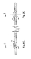
- Integrated circuit 16 includes an integrated circuit die 18 formed of a semiconductor material. Die 18 is sandwiched between non-conductive substrates 20, 22, which can be formed of a ceramic material.
- Each of substrates 20, 22 can include a respective layer of solderable material 24, 26 on the outer surfaces thereof. Pressure attached applications may not require solderable material 24, 26 on the outer surface. Elimination of solderable material 24 and 26 reduces the thermal resistance and device temperature.
- Electrode 28 is attached to an inner surface 32 of substrate 20.
- element 28 is in the form of a substrate, while element 30 may better be described as an electrical contact pad.
- Each of elements 28, 30 are electrically connected to other circuit elements within package 10, although elements 28, 30 can be electrically isolated from each other.
- Element 28 is in electrical communication with each of a distal end 34 of leadframe 12 and die 18.
- Element 30 is in electrical communication with a distal end 36 of leadframe 14.
- FIG. 1B there may be a layer 38 of electrically conductive attachment material disposed between element 28 and distal end 34 of leadframe 12. There may also be a layer 40 of electrically conductive attachment material disposed between element 30 and distal end 36 of leadframe 14, as shown in FIG. 1A.
- Electrode 42, 44 are attached to an inner surface 46 of substrate 22.
- element 44 is in the form of a substrate, while element 42 may better be described as an electrical contact pad.
- Each of elements 42, 44 are electrically connected to other circuit elements within package 10, although elements 42, 44 can be electrically isolated from each other.
- Element 44 is in electrical communication with each of a distal end 36 of leadframe 14 and die 18.
- Element 42 is in electrical communication with a distal end 34 of leadframe 12.
- a layer 48 of electrically conductive attachment material disposed between element 42 and distal end 34 of leadframe 12.
- a layer 50 of electrically conductive attachment material disposed between element 44 and distal end 36 of leadframe 14.
- the die attachment material of layers 38, 40, 48, 50 may be a type of solder paste, solder preform, ultra-thick thick film (UTTF), or electrically conductive adhesive, for example.
- die 18 has a thickness 52 as measured in a vertical direction.
- the thickness of die 18 limits how close together elements 28, 42 can be placed. More particularly, a distance between layers of attachment material 38, 48 is no less than thickness 52.
- a thickness 54 of a base portion 56 of a leadframe member 58 is not sufficiently large to perform any necessary bridging of the gap between layers of attachment material 38, 48. That is, it may be necessary for leadframe 12 to be in electrical communication with each of elements 28, 42.
- distal end 34 of leadframe member 58 is provided with an undulation 60 that, together with base portion 56, provides distal end 34 with a thickness greater than that of base portion 56 alone.
- undulation 60 together with base portion 56 provides distal end 34 with a thickness approximately equal to or slightly greater than thickness 52 of die 18.
- distal end 34 can simultaneously contact conductive attachment layers 38, 48 as well as enable desired thicknesses of layers 38, 48 to be maintained.
- An undulation such as undulation 60 may be provided below base portion 56, as is the case with leadframe 12.
- an undulation may be provided above base portion 56, as is the case with leadframe 14 as shown in FIG. 1A.
- Machine 62 that can be used in forming undulations such as undulation 60 is shown in FIG. 2.
- Machine 62 includes a piston 64 that can drive a punch 66 in direction 68 to extrude or otherwise create an undulation 70 in an otherwise planar sheet 72 of copper stock from which a leadframe can be formed.
- the surface area of a "crest" 74 of undulation 70 as well as the effective thickness between crest 74 and an opposite base portion surface 76 can be controlled by the size and type of punch 66 and by the level of force with which punch 66 is driven.
- a solid die section (not shown) could be used to further control the size, shape, and thickness of undulation 70.
- Progressive die machine 62 or a similar progressive die machine, can be used to form or punch out the entire leadframe from a sheet of copper stock.
- FIGS. 3-8 Various embodiments of a leadframe of the present invention including a member having an undulated distal end will now be described with reference to FIGS. 3-8.
- Each of the leadframe embodiments is suitable for use in conjunction with integrated circuit 16. It should be understood that although all of the leadframes of FIGS. 3-8 are shown with upwardly extending undulations, they can be easily modified within the scope of the invention to extend in a downward direction, i.e., in a direction away from the leadframe body.
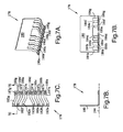
- FIGS. 3A-D illustrate one embodiment of a leadframe 78 of the present invention including a body 80 and a plurality of members 82a-g having proximal ends 84a-g and distal ends or "leads" 86a-g.
- leads 86a-g is offset formed such that the leads ramp up from the level of base portions 88a-g to a slightly higher vertical level, thereby providing leads 86a-g with undulations 90a-g.
- Undulations 90a-g and base portions 88a-g provide distal ends 86a-g with effective thicknesses greater than the thicknesses of base portions 88a-g alone.
- Each of leads 86a-g has a width in direction 92 that is greater than the width of the respective one of proximal ends 84a-g. Thus, there is ample width for leads 86a-g to ramp up to a desired vertical level without too steep of a slope.
- each of members 82a-g is bent at an angle of 90° such that distal ends 86a-g of members 82a-g extend in a direction perpendicular to body 80.
- members 82a-g define an imaginary plane 94.
- each of members 82a-g follows a bending path, i.e., is nonlinear, in a direction within plane 94.
- FIGS. 4A-D illustrate another embodiment of a leadframe 98 of the present invention including a body 100 and a plurality of members 102a-g having proximal ends 104a-g and distal ends or "leads" 106a-g.
- leads 106a-g is offset formed such that the leads ramp up from the level of base portions 108a-g to a slightly higher vertical level, thereby providing leads 106a-g with undulations 110a-g.
- Undulations 110a-g and base portions 108a-g provide distal ends 106a-g with effective thicknesses greater than the thicknesses of base portions 108a-g alone.
- Each of leads 106a-g ramps up in a direction 112 that is parallel to a direction in which members 102a-g generally extend.
- the machining of slits 113a-g and the punching of undulations 110a-g is facilitated, i.e., made easier.
- each of members 102a-g is bent at an angle of 90° such that distal ends 106a-g of members 102a-g extend in a direction perpendicular to body 100.
- members 102a-g define an imaginary plane 114.
- each of members 102a-g follows a bending path, i.e., is nonlinear, in a direction within plane 114.
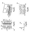
- FIGS. 5A-D illustrate yet another embodiment of a leadframe 118 of the present invention including a body 120 and a plurality of members 122a-g having proximal ends 124a-g and distal ends or "leads" 126a-g.
- leads 126a-g is corrugated formed such that the leads ramp up from the level of base portions 128a-g to a slightly higher vertical level, and then ramp back down to the level of base portions 128a-g, thereby providing leads 126a-g with undulations 130a-g.
- Undulations 130a-g and base portions 128a-g provide distal ends 126a-g with effective thicknesses greater than the thicknesses of base portions 128a-g alone.
- Each of leads 126a-g ramps up and down in a direction 132 that is parallel to a direction in which members 122a-g generally extend. Thus, the punching of undulations 130a-g is facilitated, i.e., made easier.
- each of members 122a-g is bent at an angle of 90° such that distal ends 126a-g of members 122a-g extend in a direction perpendicular to body 120.
- members 122a-g define an imaginary plane 134.
- each of members 122a-g follows a bending path, i.e., is nonlinear, in a direction within plane 134.
- FIGS. 5E-G Various additional embodiments of corrugated formed distal ends 136, 138 and 140 are shown in FIGS. 5E-G.
- Distal ends of leadframe members may have a single undulation, as is the case with the single undulation 130 on each of members 122a-g in FIGS. 5A-D.
- distal ends of leadframe member may have multiple undulations, as is the case with each of corrugated formed distal ends 136, 138 and 140.
- the undulations may be in the form of a sinusoidal wave, as with distal end 136; a triangle wave, as with distal end 138; or a substantially square wave, as with distal end 140, for example.
- a characteristic of corrugated undulations is that the undulation can extend completely across the width of the distal end in direction 142.
- FIGS. 6A-D illustrate a further embodiment of a leadframe 148 of the present invention including a body 150 and a plurality of members 152a-g having proximal ends 154a-g and distal ends or "leads" 156a-g.
- leads 156a-g is squirt formed such that the leads have dome-like bumps, thereby providing leads 156a-g with undulations 160a-g.
- Undulations 160a-g and base portions 158a-g provide distal ends 156a-g with effective thicknesses greater than the thicknesses of base portions 158a-g alone.
- each of members 152a-g is bent at an angle of 90° such that distal ends 156a-g of members 152a-g extend in a direction perpendicular to body 150.
- members 152a-g define an imaginary plane 164.
- each of members 152a-g follows a bending path, i.e., is nonlinear, in a direction within plane 164.
- the punch of the progressive die may form a squirt formed undulation having a concave, rounded cavity 166 or a trapezoidal cavity 168.
- a characteristic of squirt formed leads is that the depth of the cavity may be less than the thickness of the base portion.
- the depths of cavities 166, 168 in direction 170 is less than a thickness 172 of respective base portions 174, 176.
- FIGS. 7A-D illustrate still another embodiment of a leadframe 178 of the present invention including a body 180 and a plurality of members 182a-g having proximal ends 184a-g and distal ends or "leads" 186a-g.
- leads 186a-g is embossed formed such that the leads have bumps that are dome-like with the exception that they can have flat tops 187a-g, thereby providing leads 186a-g with undulations 190a-g.
- Undulations 190a-g and base portions 188a-g provide distal ends 186a-g with effective thicknesses greater than the thicknesses of base portions 188a-g alone.
- each of members 182a-g is bent at an angle of 90° such that distal ends 186a-g of members 182a-g extend in a direction perpendicular to body 180.
- members 182a-g define an imaginary plane 194.
- each of members 182a-g follows a bending path, i.e., is nonlinear, in a direction within plane 194.
- an embossed formed undulation can have an effective height 196 that is greater than twice a thickness 198 of a base portion 200.
- a characteristic of embossed formed leads is that the depth of the cavity may be greater than the thickness of the base portion. For example, the depths of cavity 202 in direction 204 is greater than a thickness 198 of base portion 200.
- FIGS. 8A-D illustrate still another embodiment of a leadframe 208 of the present invention including a body 210 and a plurality of members 212a-g having proximal ends 214a-g and distal ends or "leads" 216a-g.
- leads 216a-g is embossed formed such that the leads have oblong bumps that can have flat tops 217a-g and open ends 219a-g, thereby providing leads 216a-g with undulations 220a-g.
- Undulations 220a-g and base portions 218a-g provide distal ends 216a-g with effective thicknesses greater than the thicknesses of base portions 218a-g alone.
- each of members 212a-g is bent at an angle of 90° such that distal ends 216a-g of members 212a-g extend in a direction perpendicular to body 210.
- members 212a-g define an imaginary plane 224.
- each of members 212a-g follows a bending path, i.e., is nonlinear, in a direction within plane 224.
- an embossed formed, open-ended undulation can have an effective height 226 that is greater than twice a thickness 228 of a base portion 230.
- a characteristic of embossed formed leads is that the depth of the cavity may be greater than the thickness of the base portion. For example, the depths of cavity 232 in direction 234 is greater than a thickness 228 of base portion 230.
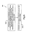
- a body portion is formed with a plurality of members extending from the body, with each of the members having a proximal end and a distal end.
- a progressive die machine such as machine 62 (FIG. 2) can form a body 80 (FIG. 3A), for example, with members 82a-g extending from body 80.
- a punch (not shown) that is designed for the particular application can be used in machine 62 to form body 80 and members 82a-g from a sheet of copper stock.
- Members 82a-g have proximal ends 84a-g and distal ends 86a-g.
- a second step S904 an undulation is formed in each of the distal ends.
- undulations 90a-g can be formed in distal ends 86a-g by inserting in machine 62 a punch (not shown) that is designed to form undulations 90a-g.
- the leadframe members can be bent at an angle of approximately 90° such that the distal ends of the members extend in a direction substantially perpendicular to the body of the leadframe.
Landscapes
- Lead Frames For Integrated Circuits (AREA)
Abstract
Description
Claims (20)
- An integrated circuit package (10), characterized by a first non-conductive substrate (20) having a first inner surface (32); a second non-conductive substrate (22) having a second inner surface (46); a die (18) disposed between said first and second inner surfaces, said die having a first thickness (52); and a leadframe (12) including a member (58) having a proximal end and a distal end, said proximal end having a second thickness (54) less than said first thickness, said distal end being disposed between said first and second inner surfaces, said distal end being undulated such that said distal end has an effective thickness greater than said second thickness.
- The package of claim 1 characterized in that said effective thickness is approximately equal to said first thickness.
- The package of claim 1 characterized in that said distal end is one of offset formed, squirt formed, corrugated formed, and embossed formed.
- The package of claim 1 characterized by at least one first conductive element (28, 30) attached to said first inner surface and in electrical communication with each of said distal end of said member and said die; and at least one second conductive element (42, 44) attached to said second inner surface and in electrical communication with each of said distal end of said member and said die.
- The package of claim 4 characterized in that said at least one first conductive element comprises at least one first bonded copper element, said at least one second conductive element comprising at least one second bonded copper element.
- The package of claim 4 characterized by at least one first layer of conductive attachment material (38, 40) disposed between said at least one first conductive element and each of said distal end of said member and said die; and at least one second layer of conductive attachment material (48, 50) disposed between said at least one second conductive element and each of said distal end of said member and said die.
- A lead frame (78) characterized by a body portion (80); and a plurality of members (82) extending from said body portion, each said member having a proximal end (84) and a distal end (86), said proximal end having a first thickness, said distal end being undulated such that said distal end has an effective thickness greater than said first thickness.
- The lead frame of claim 7 characterized in that said distal end is offset formed.
- The lead frame of claim 7 characterized in that said distal end is corrugated formed.
- The lead frame of claim 7 characterized in that said distal end is squirt formed.
- The lead frame of claim 7 characterized in that said distal end is embossed formed.
- The lead frame of claim 7 characterized in that each of said members is bent at an angle of approximately 90° such that said distal ends of said members extend in a direction substantially perpendicular to said body.
- The lead frame of claim 7 characterized in that said plurality of members define a plane (94), each of said members being nonlinear in a direction within said plane.
- A method of manufacturing a lead frame (78), characterized by forming a body portion (80) and a plurality of members (82) extending from said body portion, each of said members having a proximal end (84) and a distal end (86); and forming an undulation (90) in each of said distal ends.
- The method of claim 14 characterized in that said forming step includes providing each of said distal ends with an effective height substantially matching a second thickness of a die (18) in an integrated circuit package (10) in which said distal ends are to be inserted.
- The method of claim 14 characterized in that both of said forming steps is performed with a progressive die (62).
- The method of claim 14 characterized in that said distal end is one of offset formed, squirt formed, corrugated formed, and embossed formed.
- The method of claim 14 characterized by the further step of bending each of said members at an angle of approximately 90° such that said distal ends of said members extend in a direction substantially perpendicular to said body.
- The method of claim 14 characterized in that said plurality of members define a plane (94), each of said members being nonlinear in a direction within said plane.
- The method of claim 14 characterized in that said step of forming an undulation includes punching each of said distal ends.
Applications Claiming Priority (2)
| Application Number | Priority Date | Filing Date | Title |
|---|---|---|---|
| US780163 | 2001-02-09 | ||
| US10/780,163 US7148564B2 (en) | 2004-02-17 | 2004-02-17 | Dual-sided substrate integrated circuit package including a leadframe having leads with increased thickness |
Publications (3)
| Publication Number | Publication Date |
|---|---|
| EP1564811A2 true EP1564811A2 (en) | 2005-08-17 |
| EP1564811A3 EP1564811A3 (en) | 2007-08-08 |
| EP1564811B1 EP1564811B1 (en) | 2012-01-11 |
Family
ID=34701440
Family Applications (1)
| Application Number | Title | Priority Date | Filing Date |
|---|---|---|---|
| EP05075241A Expired - Lifetime EP1564811B1 (en) | 2004-02-17 | 2005-01-31 | Dual-sided substrate integrated circuit package including a leadframe having leads with increased thickness |
Country Status (3)
| Country | Link |
|---|---|
| US (4) | US7148564B2 (en) |
| EP (1) | EP1564811B1 (en) |
| AT (1) | ATE541313T1 (en) |
Families Citing this family (6)
| Publication number | Priority date | Publication date | Assignee | Title |
|---|---|---|---|---|
| US7148564B2 (en) * | 2004-02-17 | 2006-12-12 | Delphi Technologies, Inc. | Dual-sided substrate integrated circuit package including a leadframe having leads with increased thickness |
| JP2006222406A (en) * | 2004-08-06 | 2006-08-24 | Denso Corp | Semiconductor device |
| US20080054496A1 (en) | 2006-08-30 | 2008-03-06 | Neill Thornton | High temperature operating package and circuit design |
| US20090001546A1 (en) * | 2007-06-28 | 2009-01-01 | Flederbach Lynda G | Ultra-thick thick film on ceramic substrate |
| WO2016145526A1 (en) | 2015-03-16 | 2016-09-22 | Dana Canada Corporation | Heat exchangers with plates having surface patterns for enhancing flatness and methods for manufacturing same |
| KR102733494B1 (en) * | 2020-02-13 | 2024-11-25 | 엘지마그나 이파워트레인 주식회사 | Power module |
Family Cites Families (21)
| Publication number | Priority date | Publication date | Assignee | Title |
|---|---|---|---|---|
| US3945808A (en) * | 1974-04-15 | 1976-03-23 | Amp Incorporated | Lead frame adapted for electrical switch package |
| JPS62254457A (en) * | 1986-04-28 | 1987-11-06 | Nec Corp | Lead frame for integrated circuit |
| US5166098A (en) * | 1988-03-05 | 1992-11-24 | Deutsche Itt Industries Gmbh | Method of manufacturing an encapsulated semiconductor device with a can type housing |
| JPH0547980A (en) * | 1991-08-08 | 1993-02-26 | Sumitomo Metal Mining Co Ltd | Ic lead frame for semiconductor device |
| JPH06252334A (en) * | 1993-02-26 | 1994-09-09 | Hitachi Constr Mach Co Ltd | Semiconductor device |
| US5340771A (en) * | 1993-03-18 | 1994-08-23 | Lsi Logic Corporation | Techniques for providing high I/O count connections to semiconductor dies |
| KR100386061B1 (en) * | 1995-10-24 | 2003-08-21 | 오끼 덴끼 고오교 가부시끼가이샤 | Semiconductor device and lead frame with improved construction to prevent cracking |
| KR100186309B1 (en) * | 1996-05-17 | 1999-03-20 | 문정환 | Stacked bottom lead package |
| US5677567A (en) * | 1996-06-17 | 1997-10-14 | Micron Technology, Inc. | Leads between chips assembly |
| US6072228A (en) * | 1996-10-25 | 2000-06-06 | Micron Technology, Inc. | Multi-part lead frame with dissimilar materials and method of manufacturing |
| JP3487173B2 (en) * | 1997-05-26 | 2004-01-13 | セイコーエプソン株式会社 | TAB tape carrier, integrated circuit device and electronic equipment |
| JPH11288751A (en) * | 1998-04-03 | 1999-10-19 | Alps Electric Co Ltd | Terminal mounting structure on printed wiring board |
| US6122822A (en) * | 1998-06-23 | 2000-09-26 | Vanguard International Semiconductor Corporation | Method for balancing mold flow in encapsulating devices |
| US6307755B1 (en) * | 1999-05-27 | 2001-10-23 | Richard K. Williams | Surface mount semiconductor package, die-leadframe combination and leadframe therefor and method of mounting leadframes to surfaces of semiconductor die |
| JP4416140B2 (en) * | 2000-04-14 | 2010-02-17 | 日本インター株式会社 | Resin-sealed semiconductor device |
| US6781225B2 (en) * | 2000-09-15 | 2004-08-24 | Chipmos Technologies Inc. | Glueless integrated circuit system in a packaging module |
| US6459148B1 (en) * | 2000-11-13 | 2002-10-01 | Walsin Advanced Electronics Ltd | QFN semiconductor package |
| US6812553B2 (en) * | 2002-01-16 | 2004-11-02 | Delphi Technologies, Inc. | Electrically isolated and thermally conductive double-sided pre-packaged component |
| TW540123B (en) * | 2002-06-14 | 2003-07-01 | Siliconware Precision Industries Co Ltd | Flip-chip semiconductor package with lead frame as chip carrier |
| US7148564B2 (en) * | 2004-02-17 | 2006-12-12 | Delphi Technologies, Inc. | Dual-sided substrate integrated circuit package including a leadframe having leads with increased thickness |
| US7202105B2 (en) * | 2004-06-28 | 2007-04-10 | Semiconductor Components Industries, L.L.C. | Multi-chip semiconductor connector assembly method |
-
2004
- 2004-02-17 US US10/780,163 patent/US7148564B2/en not_active Expired - Lifetime
-
2005
- 2005-01-31 AT AT05075241T patent/ATE541313T1/en active
- 2005-01-31 EP EP05075241A patent/EP1564811B1/en not_active Expired - Lifetime
-
2006
- 2006-10-05 US US11/543,605 patent/US20070069348A1/en not_active Abandoned
-
2008
- 2008-04-24 US US12/150,070 patent/US7697303B2/en not_active Expired - Lifetime
-
2010
- 2010-02-02 US US12/698,644 patent/US20100133672A1/en not_active Abandoned
Also Published As
| Publication number | Publication date |
|---|---|
| US7148564B2 (en) | 2006-12-12 |
| US20070069348A1 (en) | 2007-03-29 |
| EP1564811A3 (en) | 2007-08-08 |
| ATE541313T1 (en) | 2012-01-15 |
| US20050179123A1 (en) | 2005-08-18 |
| US20080198568A1 (en) | 2008-08-21 |
| EP1564811B1 (en) | 2012-01-11 |
| US20100133672A1 (en) | 2010-06-03 |
| US7697303B2 (en) | 2010-04-13 |
Similar Documents
| Publication | Publication Date | Title |
|---|---|---|
| JP2934202B2 (en) | Method for forming conductive bumps on wiring board | |
| US7697303B2 (en) | Dual-sided substrate integrated circuit package including a leadframe having leads with increased thickness | |
| TWI311836B (en) | Electrical connecting member capable of achieving stable connection with a simple structure and connector using the same | |
| CN1110772C (en) | chip module | |
| CN100461353C (en) | Method for manufacturing hybrid integrated circuit device | |
| EP1304740A3 (en) | Circuit board, method for manufacturing same, and high-output module | |
| JP5433526B2 (en) | Electronic device and manufacturing method thereof | |
| JP2008177461A (en) | Electronic device and manufacturing method thereof | |
| KR20050011714A (en) | Power semiconductor module with base plate resistant to bending | |
| US6803648B1 (en) | Integrated circuit packages with interconnects on top and bottom surfaces | |
| KR100457029B1 (en) | Land grid array type semiconductor device and method of mounting the same | |
| EP1610381A3 (en) | Electronic package employing segmented connector and solder joint | |
| US7661964B2 (en) | Connecting parts and multilayer wiring board | |
| KR20020034923A (en) | Method for the manufacture of a metal support frame, said metal support frame and use thereof | |
| JP2010078541A (en) | Wiring board, manufacturing method therefor, multilayer wiring board, and probe card | |
| US7560809B2 (en) | Semiconductor device | |
| EP1480267A2 (en) | Integrated electronic component | |
| CN1458688A (en) | Electronic module | |
| US7504713B2 (en) | Plastic semiconductor packages having improved metal land-locking features | |
| US20040065953A1 (en) | Semiconductor device and process of manufacture | |
| US20080290481A1 (en) | Semiconductor Device Package Leadframe | |
| JPH09214093A (en) | Mounted circuit device and manufacturing method thereof | |
| JPH08330501A (en) | Semiconductor lead frame and manufacturing method thereof | |
| JP2954559B2 (en) | Wiring board electrode structure | |
| US20050189625A1 (en) | Lead-frame for electonic devices with extruded pads |
Legal Events
| Date | Code | Title | Description |
|---|---|---|---|
| PUAI | Public reference made under article 153(3) epc to a published international application that has entered the european phase |
Free format text: ORIGINAL CODE: 0009012 |
|
| AK | Designated contracting states |
Kind code of ref document: A2 Designated state(s): AT BE BG CH CY CZ DE DK EE ES FI FR GB GR HU IE IS IT LI LT LU MC NL PL PT RO SE SI SK TR |
|
| AX | Request for extension of the european patent |
Extension state: AL BA HR LV MK YU |
|
| PUAL | Search report despatched |
Free format text: ORIGINAL CODE: 0009013 |
|
| AK | Designated contracting states |
Kind code of ref document: A3 Designated state(s): AT BE BG CH CY CZ DE DK EE ES FI FR GB GR HU IE IS IT LI LT LU MC NL PL PT RO SE SI SK TR |
|
| AX | Request for extension of the european patent |
Extension state: AL BA HR LV MK YU |
|
| 17P | Request for examination filed |
Effective date: 20080208 |
|
| AKX | Designation fees paid |
Designated state(s): AT BE BG CH CY CZ DE DK EE ES FI FR GB GR HU IE IS IT LI LT LU MC NL PL PT RO SE SI SK TR |
|
| 17Q | First examination report despatched |
Effective date: 20091106 |
|
| GRAP | Despatch of communication of intention to grant a patent |
Free format text: ORIGINAL CODE: EPIDOSNIGR1 |
|
| GRAS | Grant fee paid |
Free format text: ORIGINAL CODE: EPIDOSNIGR3 |
|
| GRAA | (expected) grant |
Free format text: ORIGINAL CODE: 0009210 |
|
| AK | Designated contracting states |
Kind code of ref document: B1 Designated state(s): AT BE BG CH CY CZ DE DK EE ES FI FR GB GR HU IE IS IT LI LT LU MC NL PL PT RO SE SI SK TR |
|
| REG | Reference to a national code |
Ref country code: GB Ref legal event code: FG4D |
|
| REG | Reference to a national code |
Ref country code: CH Ref legal event code: EP |
|
| REG | Reference to a national code |
Ref country code: AT Ref legal event code: REF Ref document number: 541313 Country of ref document: AT Kind code of ref document: T Effective date: 20120115 |
|
| REG | Reference to a national code |
Ref country code: IE Ref legal event code: FG4D |
|
| REG | Reference to a national code |
Ref country code: DE Ref legal event code: R096 Ref document number: 602005032066 Country of ref document: DE Effective date: 20120308 |
|
| REG | Reference to a national code |
Ref country code: NL Ref legal event code: VDEP Effective date: 20120111 |
|
| PG25 | Lapsed in a contracting state [announced via postgrant information from national office to epo] |
Ref country code: SI Free format text: LAPSE BECAUSE OF FAILURE TO SUBMIT A TRANSLATION OF THE DESCRIPTION OR TO PAY THE FEE WITHIN THE PRESCRIBED TIME-LIMIT Effective date: 20120111 |
|
| LTIE | Lt: invalidation of european patent or patent extension |
Effective date: 20120111 |
|
| PG25 | Lapsed in a contracting state [announced via postgrant information from national office to epo] |
Ref country code: NL Free format text: LAPSE BECAUSE OF FAILURE TO SUBMIT A TRANSLATION OF THE DESCRIPTION OR TO PAY THE FEE WITHIN THE PRESCRIBED TIME-LIMIT Effective date: 20120111 Ref country code: BE Free format text: LAPSE BECAUSE OF FAILURE TO SUBMIT A TRANSLATION OF THE DESCRIPTION OR TO PAY THE FEE WITHIN THE PRESCRIBED TIME-LIMIT Effective date: 20120111 Ref country code: LT Free format text: LAPSE BECAUSE OF FAILURE TO SUBMIT A TRANSLATION OF THE DESCRIPTION OR TO PAY THE FEE WITHIN THE PRESCRIBED TIME-LIMIT Effective date: 20120111 Ref country code: BG Free format text: LAPSE BECAUSE OF FAILURE TO SUBMIT A TRANSLATION OF THE DESCRIPTION OR TO PAY THE FEE WITHIN THE PRESCRIBED TIME-LIMIT Effective date: 20120411 Ref country code: IS Free format text: LAPSE BECAUSE OF FAILURE TO SUBMIT A TRANSLATION OF THE DESCRIPTION OR TO PAY THE FEE WITHIN THE PRESCRIBED TIME-LIMIT Effective date: 20120511 |
|
| PG25 | Lapsed in a contracting state [announced via postgrant information from national office to epo] |
Ref country code: GR Free format text: LAPSE BECAUSE OF FAILURE TO SUBMIT A TRANSLATION OF THE DESCRIPTION OR TO PAY THE FEE WITHIN THE PRESCRIBED TIME-LIMIT Effective date: 20120412 Ref country code: MC Free format text: LAPSE BECAUSE OF NON-PAYMENT OF DUE FEES Effective date: 20120131 Ref country code: FI Free format text: LAPSE BECAUSE OF FAILURE TO SUBMIT A TRANSLATION OF THE DESCRIPTION OR TO PAY THE FEE WITHIN THE PRESCRIBED TIME-LIMIT Effective date: 20120111 Ref country code: PT Free format text: LAPSE BECAUSE OF FAILURE TO SUBMIT A TRANSLATION OF THE DESCRIPTION OR TO PAY THE FEE WITHIN THE PRESCRIBED TIME-LIMIT Effective date: 20120511 Ref country code: PL Free format text: LAPSE BECAUSE OF FAILURE TO SUBMIT A TRANSLATION OF THE DESCRIPTION OR TO PAY THE FEE WITHIN THE PRESCRIBED TIME-LIMIT Effective date: 20120111 |
|
| REG | Reference to a national code |
Ref country code: CH Ref legal event code: PL |
|
| REG | Reference to a national code |
Ref country code: AT Ref legal event code: MK05 Ref document number: 541313 Country of ref document: AT Kind code of ref document: T Effective date: 20120111 |
|
| PG25 | Lapsed in a contracting state [announced via postgrant information from national office to epo] |
Ref country code: CY Free format text: LAPSE BECAUSE OF FAILURE TO SUBMIT A TRANSLATION OF THE DESCRIPTION OR TO PAY THE FEE WITHIN THE PRESCRIBED TIME-LIMIT Effective date: 20120111 |
|
| REG | Reference to a national code |
Ref country code: IE Ref legal event code: MM4A |
|
| PG25 | Lapsed in a contracting state [announced via postgrant information from national office to epo] |
Ref country code: LI Free format text: LAPSE BECAUSE OF NON-PAYMENT OF DUE FEES Effective date: 20120131 Ref country code: RO Free format text: LAPSE BECAUSE OF FAILURE TO SUBMIT A TRANSLATION OF THE DESCRIPTION OR TO PAY THE FEE WITHIN THE PRESCRIBED TIME-LIMIT Effective date: 20120111 Ref country code: SE Free format text: LAPSE BECAUSE OF FAILURE TO SUBMIT A TRANSLATION OF THE DESCRIPTION OR TO PAY THE FEE WITHIN THE PRESCRIBED TIME-LIMIT Effective date: 20120111 Ref country code: DK Free format text: LAPSE BECAUSE OF FAILURE TO SUBMIT A TRANSLATION OF THE DESCRIPTION OR TO PAY THE FEE WITHIN THE PRESCRIBED TIME-LIMIT Effective date: 20120111 Ref country code: CZ Free format text: LAPSE BECAUSE OF FAILURE TO SUBMIT A TRANSLATION OF THE DESCRIPTION OR TO PAY THE FEE WITHIN THE PRESCRIBED TIME-LIMIT Effective date: 20120111 Ref country code: EE Free format text: LAPSE BECAUSE OF FAILURE TO SUBMIT A TRANSLATION OF THE DESCRIPTION OR TO PAY THE FEE WITHIN THE PRESCRIBED TIME-LIMIT Effective date: 20120111 Ref country code: CH Free format text: LAPSE BECAUSE OF NON-PAYMENT OF DUE FEES Effective date: 20120131 |
|
| PLBE | No opposition filed within time limit |
Free format text: ORIGINAL CODE: 0009261 |
|
| STAA | Information on the status of an ep patent application or granted ep patent |
Free format text: STATUS: NO OPPOSITION FILED WITHIN TIME LIMIT |
|
| PG25 | Lapsed in a contracting state [announced via postgrant information from national office to epo] |
Ref country code: IT Free format text: LAPSE BECAUSE OF FAILURE TO SUBMIT A TRANSLATION OF THE DESCRIPTION OR TO PAY THE FEE WITHIN THE PRESCRIBED TIME-LIMIT Effective date: 20120111 Ref country code: SK Free format text: LAPSE BECAUSE OF FAILURE TO SUBMIT A TRANSLATION OF THE DESCRIPTION OR TO PAY THE FEE WITHIN THE PRESCRIBED TIME-LIMIT Effective date: 20120111 |
|
| 26N | No opposition filed |
Effective date: 20121012 |
|
| GBPC | Gb: european patent ceased through non-payment of renewal fee |
Effective date: 20120411 |
|
| PG25 | Lapsed in a contracting state [announced via postgrant information from national office to epo] |
Ref country code: IE Free format text: LAPSE BECAUSE OF NON-PAYMENT OF DUE FEES Effective date: 20120131 Ref country code: AT Free format text: LAPSE BECAUSE OF FAILURE TO SUBMIT A TRANSLATION OF THE DESCRIPTION OR TO PAY THE FEE WITHIN THE PRESCRIBED TIME-LIMIT Effective date: 20120111 Ref country code: GB Free format text: LAPSE BECAUSE OF NON-PAYMENT OF DUE FEES Effective date: 20120411 |
|
| REG | Reference to a national code |
Ref country code: DE Ref legal event code: R097 Ref document number: 602005032066 Country of ref document: DE Effective date: 20121012 |
|
| REG | Reference to a national code |
Ref country code: FR Ref legal event code: ST Effective date: 20130104 |
|
| PG25 | Lapsed in a contracting state [announced via postgrant information from national office to epo] |
Ref country code: FR Free format text: LAPSE BECAUSE OF NON-PAYMENT OF DUE FEES Effective date: 20120312 |
|
| PG25 | Lapsed in a contracting state [announced via postgrant information from national office to epo] |
Ref country code: ES Free format text: LAPSE BECAUSE OF FAILURE TO SUBMIT A TRANSLATION OF THE DESCRIPTION OR TO PAY THE FEE WITHIN THE PRESCRIBED TIME-LIMIT Effective date: 20120422 |
|
| PG25 | Lapsed in a contracting state [announced via postgrant information from national office to epo] |
Ref country code: TR Free format text: LAPSE BECAUSE OF FAILURE TO SUBMIT A TRANSLATION OF THE DESCRIPTION OR TO PAY THE FEE WITHIN THE PRESCRIBED TIME-LIMIT Effective date: 20120111 |
|
| PG25 | Lapsed in a contracting state [announced via postgrant information from national office to epo] |
Ref country code: LU Free format text: LAPSE BECAUSE OF NON-PAYMENT OF DUE FEES Effective date: 20120131 |
|
| PG25 | Lapsed in a contracting state [announced via postgrant information from national office to epo] |
Ref country code: HU Free format text: LAPSE BECAUSE OF FAILURE TO SUBMIT A TRANSLATION OF THE DESCRIPTION OR TO PAY THE FEE WITHIN THE PRESCRIBED TIME-LIMIT Effective date: 20050131 |
|
| REG | Reference to a national code |
Ref country code: DE Ref legal event code: R081 Ref document number: 602005032066 Country of ref document: DE Owner name: DELPHI TECHNOLOGIES IP LIMITED, BB Free format text: FORMER OWNER: DELPHI TECHNOLOGIES, INC., TROY, MICH., US |
|
| P01 | Opt-out of the competence of the unified patent court (upc) registered |
Effective date: 20230327 |
|
| PGFP | Annual fee paid to national office [announced via postgrant information from national office to epo] |
Ref country code: DE Payment date: 20231215 Year of fee payment: 20 |
|
| REG | Reference to a national code |
Ref country code: DE Ref legal event code: R071 Ref document number: 602005032066 Country of ref document: DE |