EP1562168A2 - Elektrolumineszente Anzeigevorrichtung und Ansteuerverfahren dafür - Google Patents
Elektrolumineszente Anzeigevorrichtung und Ansteuerverfahren dafür Download PDFInfo
- Publication number
- EP1562168A2 EP1562168A2 EP05002000A EP05002000A EP1562168A2 EP 1562168 A2 EP1562168 A2 EP 1562168A2 EP 05002000 A EP05002000 A EP 05002000A EP 05002000 A EP05002000 A EP 05002000A EP 1562168 A2 EP1562168 A2 EP 1562168A2
- Authority
- EP
- European Patent Office
- Prior art keywords
- electro
- signal
- voltage source
- thin film
- film transistor
- Prior art date
- Legal status (The legal status is an assumption and is not a legal conclusion. Google has not performed a legal analysis and makes no representation as to the accuracy of the status listed.)
- Withdrawn
Links
- 238000005401 electroluminescence Methods 0.000 title claims abstract description 205
- 238000000034 method Methods 0.000 title claims abstract description 48
- 239000010409 thin film Substances 0.000 claims abstract description 153
- 230000001360 synchronised effect Effects 0.000 claims description 15
- 239000003990 capacitor Substances 0.000 claims description 13
- 230000004044 response Effects 0.000 claims description 8
- 230000006866 deterioration Effects 0.000 abstract description 7
- 230000003044 adaptive effect Effects 0.000 abstract description 3
- 102100036285 25-hydroxyvitamin D-1 alpha hydroxylase, mitochondrial Human genes 0.000 description 30
- 101000875403 Homo sapiens 25-hydroxyvitamin D-1 alpha hydroxylase, mitochondrial Proteins 0.000 description 30
- 238000010586 diagram Methods 0.000 description 16
- 229910021420 polycrystalline silicon Inorganic materials 0.000 description 7
- 229920005591 polysilicon Polymers 0.000 description 7
- 230000008859 change Effects 0.000 description 6
- 229910021417 amorphous silicon Inorganic materials 0.000 description 4
- 239000013078 crystal Substances 0.000 description 4
- 238000002347 injection Methods 0.000 description 4
- 239000007924 injection Substances 0.000 description 4
- 108091006149 Electron carriers Proteins 0.000 description 3
- 230000008901 benefit Effects 0.000 description 3
- 230000008569 process Effects 0.000 description 3
- 239000004065 semiconductor Substances 0.000 description 3
- 239000011521 glass Substances 0.000 description 2
- BHEPBYXIRTUNPN-UHFFFAOYSA-N hydridophosphorus(.) (triplet) Chemical compound [PH] BHEPBYXIRTUNPN-UHFFFAOYSA-N 0.000 description 2
- 238000005286 illumination Methods 0.000 description 2
- 239000000463 material Substances 0.000 description 2
- 230000003287 optical effect Effects 0.000 description 2
- 239000000758 substrate Substances 0.000 description 2
- XUIMIQQOPSSXEZ-UHFFFAOYSA-N Silicon Chemical compound [Si] XUIMIQQOPSSXEZ-UHFFFAOYSA-N 0.000 description 1
- 230000015572 biosynthetic process Effects 0.000 description 1
- 239000002800 charge carrier Substances 0.000 description 1
- 238000001816 cooling Methods 0.000 description 1
- 230000007423 decrease Effects 0.000 description 1
- 150000002484 inorganic compounds Chemical class 0.000 description 1
- 229910010272 inorganic material Inorganic materials 0.000 description 1
- 230000010354 integration Effects 0.000 description 1
- 230000001788 irregular Effects 0.000 description 1
- 238000005224 laser annealing Methods 0.000 description 1
- 239000004973 liquid crystal related substance Substances 0.000 description 1
- 238000004020 luminiscence type Methods 0.000 description 1
- 239000011159 matrix material Substances 0.000 description 1
- 239000000155 melt Substances 0.000 description 1
- 230000004048 modification Effects 0.000 description 1
- 238000012986 modification Methods 0.000 description 1
- 150000002894 organic compounds Chemical class 0.000 description 1
- 229910052710 silicon Inorganic materials 0.000 description 1
- 239000010703 silicon Substances 0.000 description 1
- 230000003685 thermal hair damage Effects 0.000 description 1
Images






Classifications
-
- G—PHYSICS
- G09—EDUCATION; CRYPTOGRAPHY; DISPLAY; ADVERTISING; SEALS
- G09G—ARRANGEMENTS OR CIRCUITS FOR CONTROL OF INDICATING DEVICES USING STATIC MEANS TO PRESENT VARIABLE INFORMATION
- G09G3/00—Control arrangements or circuits, of interest only in connection with visual indicators other than cathode-ray tubes
- G09G3/20—Control arrangements or circuits, of interest only in connection with visual indicators other than cathode-ray tubes for presentation of an assembly of a number of characters, e.g. a page, by composing the assembly by combination of individual elements arranged in a matrix no fixed position being assigned to or needed to be assigned to the individual characters or partial characters
- G09G3/2007—Display of intermediate tones
- G09G3/2011—Display of intermediate tones by amplitude modulation
-
- G—PHYSICS
- G09—EDUCATION; CRYPTOGRAPHY; DISPLAY; ADVERTISING; SEALS
- G09G—ARRANGEMENTS OR CIRCUITS FOR CONTROL OF INDICATING DEVICES USING STATIC MEANS TO PRESENT VARIABLE INFORMATION
- G09G3/00—Control arrangements or circuits, of interest only in connection with visual indicators other than cathode-ray tubes
- G09G3/20—Control arrangements or circuits, of interest only in connection with visual indicators other than cathode-ray tubes for presentation of an assembly of a number of characters, e.g. a page, by composing the assembly by combination of individual elements arranged in a matrix no fixed position being assigned to or needed to be assigned to the individual characters or partial characters
- G09G3/2007—Display of intermediate tones
- G09G3/2018—Display of intermediate tones by time modulation using two or more time intervals
- G09G3/2022—Display of intermediate tones by time modulation using two or more time intervals using sub-frames
-
- G—PHYSICS
- G09—EDUCATION; CRYPTOGRAPHY; DISPLAY; ADVERTISING; SEALS
- G09G—ARRANGEMENTS OR CIRCUITS FOR CONTROL OF INDICATING DEVICES USING STATIC MEANS TO PRESENT VARIABLE INFORMATION
- G09G3/00—Control arrangements or circuits, of interest only in connection with visual indicators other than cathode-ray tubes
- G09G3/20—Control arrangements or circuits, of interest only in connection with visual indicators other than cathode-ray tubes for presentation of an assembly of a number of characters, e.g. a page, by composing the assembly by combination of individual elements arranged in a matrix no fixed position being assigned to or needed to be assigned to the individual characters or partial characters
- G09G3/2007—Display of intermediate tones
- G09G3/2077—Display of intermediate tones by a combination of two or more gradation control methods
- G09G3/2081—Display of intermediate tones by a combination of two or more gradation control methods with combination of amplitude modulation and time modulation
-
- G—PHYSICS
- G09—EDUCATION; CRYPTOGRAPHY; DISPLAY; ADVERTISING; SEALS
- G09G—ARRANGEMENTS OR CIRCUITS FOR CONTROL OF INDICATING DEVICES USING STATIC MEANS TO PRESENT VARIABLE INFORMATION
- G09G3/00—Control arrangements or circuits, of interest only in connection with visual indicators other than cathode-ray tubes
- G09G3/20—Control arrangements or circuits, of interest only in connection with visual indicators other than cathode-ray tubes for presentation of an assembly of a number of characters, e.g. a page, by composing the assembly by combination of individual elements arranged in a matrix no fixed position being assigned to or needed to be assigned to the individual characters or partial characters
- G09G3/22—Control arrangements or circuits, of interest only in connection with visual indicators other than cathode-ray tubes for presentation of an assembly of a number of characters, e.g. a page, by composing the assembly by combination of individual elements arranged in a matrix no fixed position being assigned to or needed to be assigned to the individual characters or partial characters using controlled light sources
- G09G3/30—Control arrangements or circuits, of interest only in connection with visual indicators other than cathode-ray tubes for presentation of an assembly of a number of characters, e.g. a page, by composing the assembly by combination of individual elements arranged in a matrix no fixed position being assigned to or needed to be assigned to the individual characters or partial characters using controlled light sources using electroluminescent panels
- G09G3/32—Control arrangements or circuits, of interest only in connection with visual indicators other than cathode-ray tubes for presentation of an assembly of a number of characters, e.g. a page, by composing the assembly by combination of individual elements arranged in a matrix no fixed position being assigned to or needed to be assigned to the individual characters or partial characters using controlled light sources using electroluminescent panels semiconductive, e.g. using light-emitting diodes [LED]
- G09G3/3208—Control arrangements or circuits, of interest only in connection with visual indicators other than cathode-ray tubes for presentation of an assembly of a number of characters, e.g. a page, by composing the assembly by combination of individual elements arranged in a matrix no fixed position being assigned to or needed to be assigned to the individual characters or partial characters using controlled light sources using electroluminescent panels semiconductive, e.g. using light-emitting diodes [LED] organic, e.g. using organic light-emitting diodes [OLED]
- G09G3/3225—Control arrangements or circuits, of interest only in connection with visual indicators other than cathode-ray tubes for presentation of an assembly of a number of characters, e.g. a page, by composing the assembly by combination of individual elements arranged in a matrix no fixed position being assigned to or needed to be assigned to the individual characters or partial characters using controlled light sources using electroluminescent panels semiconductive, e.g. using light-emitting diodes [LED] organic, e.g. using organic light-emitting diodes [OLED] using an active matrix
- G09G3/3233—Control arrangements or circuits, of interest only in connection with visual indicators other than cathode-ray tubes for presentation of an assembly of a number of characters, e.g. a page, by composing the assembly by combination of individual elements arranged in a matrix no fixed position being assigned to or needed to be assigned to the individual characters or partial characters using controlled light sources using electroluminescent panels semiconductive, e.g. using light-emitting diodes [LED] organic, e.g. using organic light-emitting diodes [OLED] using an active matrix with pixel circuitry controlling the current through the light-emitting element
-
- G—PHYSICS
- G09—EDUCATION; CRYPTOGRAPHY; DISPLAY; ADVERTISING; SEALS
- G09G—ARRANGEMENTS OR CIRCUITS FOR CONTROL OF INDICATING DEVICES USING STATIC MEANS TO PRESENT VARIABLE INFORMATION
- G09G3/00—Control arrangements or circuits, of interest only in connection with visual indicators other than cathode-ray tubes
- G09G3/20—Control arrangements or circuits, of interest only in connection with visual indicators other than cathode-ray tubes for presentation of an assembly of a number of characters, e.g. a page, by composing the assembly by combination of individual elements arranged in a matrix no fixed position being assigned to or needed to be assigned to the individual characters or partial characters
- G09G3/22—Control arrangements or circuits, of interest only in connection with visual indicators other than cathode-ray tubes for presentation of an assembly of a number of characters, e.g. a page, by composing the assembly by combination of individual elements arranged in a matrix no fixed position being assigned to or needed to be assigned to the individual characters or partial characters using controlled light sources
- G09G3/30—Control arrangements or circuits, of interest only in connection with visual indicators other than cathode-ray tubes for presentation of an assembly of a number of characters, e.g. a page, by composing the assembly by combination of individual elements arranged in a matrix no fixed position being assigned to or needed to be assigned to the individual characters or partial characters using controlled light sources using electroluminescent panels
- G09G3/32—Control arrangements or circuits, of interest only in connection with visual indicators other than cathode-ray tubes for presentation of an assembly of a number of characters, e.g. a page, by composing the assembly by combination of individual elements arranged in a matrix no fixed position being assigned to or needed to be assigned to the individual characters or partial characters using controlled light sources using electroluminescent panels semiconductive, e.g. using light-emitting diodes [LED]
- G09G3/3208—Control arrangements or circuits, of interest only in connection with visual indicators other than cathode-ray tubes for presentation of an assembly of a number of characters, e.g. a page, by composing the assembly by combination of individual elements arranged in a matrix no fixed position being assigned to or needed to be assigned to the individual characters or partial characters using controlled light sources using electroluminescent panels semiconductive, e.g. using light-emitting diodes [LED] organic, e.g. using organic light-emitting diodes [OLED]
- G09G3/3275—Details of drivers for data electrodes
- G09G3/3291—Details of drivers for data electrodes in which the data driver supplies a variable data voltage for setting the current through, or the voltage across, the light-emitting elements
-
- G—PHYSICS
- G09—EDUCATION; CRYPTOGRAPHY; DISPLAY; ADVERTISING; SEALS
- G09G—ARRANGEMENTS OR CIRCUITS FOR CONTROL OF INDICATING DEVICES USING STATIC MEANS TO PRESENT VARIABLE INFORMATION
- G09G2300/00—Aspects of the constitution of display devices
- G09G2300/08—Active matrix structure, i.e. with use of active elements, inclusive of non-linear two terminal elements, in the pixels together with light emitting or modulating elements
- G09G2300/0809—Several active elements per pixel in active matrix panels
- G09G2300/0842—Several active elements per pixel in active matrix panels forming a memory circuit, e.g. a dynamic memory with one capacitor
-
- G—PHYSICS
- G09—EDUCATION; CRYPTOGRAPHY; DISPLAY; ADVERTISING; SEALS
- G09G—ARRANGEMENTS OR CIRCUITS FOR CONTROL OF INDICATING DEVICES USING STATIC MEANS TO PRESENT VARIABLE INFORMATION
- G09G2300/00—Aspects of the constitution of display devices
- G09G2300/08—Active matrix structure, i.e. with use of active elements, inclusive of non-linear two terminal elements, in the pixels together with light emitting or modulating elements
- G09G2300/0809—Several active elements per pixel in active matrix panels
- G09G2300/0842—Several active elements per pixel in active matrix panels forming a memory circuit, e.g. a dynamic memory with one capacitor
- G09G2300/0861—Several active elements per pixel in active matrix panels forming a memory circuit, e.g. a dynamic memory with one capacitor with additional control of the display period without amending the charge stored in a pixel memory, e.g. by means of additional select electrodes
- G09G2300/0866—Several active elements per pixel in active matrix panels forming a memory circuit, e.g. a dynamic memory with one capacitor with additional control of the display period without amending the charge stored in a pixel memory, e.g. by means of additional select electrodes by means of changes in the pixel supply voltage
-
- G—PHYSICS
- G09—EDUCATION; CRYPTOGRAPHY; DISPLAY; ADVERTISING; SEALS
- G09G—ARRANGEMENTS OR CIRCUITS FOR CONTROL OF INDICATING DEVICES USING STATIC MEANS TO PRESENT VARIABLE INFORMATION
- G09G2310/00—Command of the display device
- G09G2310/02—Addressing, scanning or driving the display screen or processing steps related thereto
- G09G2310/0264—Details of driving circuits
- G09G2310/027—Details of drivers for data electrodes, the drivers handling digital grey scale data, e.g. use of D/A converters
-
- G—PHYSICS
- G09—EDUCATION; CRYPTOGRAPHY; DISPLAY; ADVERTISING; SEALS
- G09G—ARRANGEMENTS OR CIRCUITS FOR CONTROL OF INDICATING DEVICES USING STATIC MEANS TO PRESENT VARIABLE INFORMATION
- G09G2320/00—Control of display operating conditions
- G09G2320/04—Maintaining the quality of display appearance
- G09G2320/043—Preventing or counteracting the effects of ageing
-
- G—PHYSICS
- G09—EDUCATION; CRYPTOGRAPHY; DISPLAY; ADVERTISING; SEALS
- G09G—ARRANGEMENTS OR CIRCUITS FOR CONTROL OF INDICATING DEVICES USING STATIC MEANS TO PRESENT VARIABLE INFORMATION
- G09G3/00—Control arrangements or circuits, of interest only in connection with visual indicators other than cathode-ray tubes
- G09G3/20—Control arrangements or circuits, of interest only in connection with visual indicators other than cathode-ray tubes for presentation of an assembly of a number of characters, e.g. a page, by composing the assembly by combination of individual elements arranged in a matrix no fixed position being assigned to or needed to be assigned to the individual characters or partial characters
- G09G3/34—Control arrangements or circuits, of interest only in connection with visual indicators other than cathode-ray tubes for presentation of an assembly of a number of characters, e.g. a page, by composing the assembly by combination of individual elements arranged in a matrix no fixed position being assigned to or needed to be assigned to the individual characters or partial characters by control of light from an independent source
- G09G3/36—Control arrangements or circuits, of interest only in connection with visual indicators other than cathode-ray tubes for presentation of an assembly of a number of characters, e.g. a page, by composing the assembly by combination of individual elements arranged in a matrix no fixed position being assigned to or needed to be assigned to the individual characters or partial characters by control of light from an independent source using liquid crystals
- G09G3/3611—Control of matrices with row and column drivers
- G09G3/3648—Control of matrices with row and column drivers using an active matrix
- G09G3/3655—Details of drivers for counter electrodes, e.g. common electrodes for pixel capacitors or supplementary storage capacitors
Definitions
- the present invention relates to an electro-luminescence display device, and more particularly to an electro-luminescence display device that is adaptive for preventing picture quality deterioration by operating a thin film transistor for an electro-luminescence cell drive at a non-saturation area to compensate a threshold voltage, and a driving method thereof.
- Such flat panel display devices include a liquid crystal display (LCD), a field emission display (FED), a plasma display panel (PDP) and an electro-luminescence (EL) display, etc.
- LCD liquid crystal display
- FED field emission display
- PDP plasma display panel
- EL electro-luminescence
- the EL display in such display devices is a self-luminous device capable of light-emitting a phosphorous material by a re-combination of electrons with holes.
- the EL display device is generally classified into an inorganic EL device using the phosphorous material as an inorganic compound and an organic using it as an organic compound.
- Such an EL display device has many advantages of a low voltage driving, a self-luminescence, a thin-thickness, a wide viewing angle, a fast response speed and a high contrast, etc, such that it can be highlighted into a post-generation display device.
- the organic EL device is usually comprised of an electron injection layer, an electron carrier layer, a light-emitting layer, a hole carrier layer and a hole injection layer that are disposed between a cathode and an anode.
- an organic EL device when a pre-determined voltage is applied between an anode and a cathode, electrons produced from the cathode are moved, via the electron injection layer and the electron carrier layer, into the light-emitting layer while holes produced from the anode are moved, via the hole injection layer and the hole carrier layer, into the light-emitting layer.
- the electrons and the holes fed from the electron carrier layer and the hole carrier layer emit a light by their re-combination at the light-emitting layer.
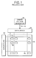
- An active matrix EL display device using such an organic EL device includes an EL panel 20 having pixel cells 28 inclusive of EL cells OLED arranged at areas defined by intersections between gate lines GL and data lines DL, a gate driver 22 to drive the gate lines GL of the EL panel 20, a data driver 24 to drive the data lines DL of the EL panel 20, and a gamma voltage generator 26 that supplies a plurality of gamma voltages VH to VL to the data driver 24.
- the gate driver 22 supplies a scan pulse to the gate lines GL to sequentially drive the gate lines GL.
- the gamma voltage generator 26 generates different gray level gamma voltages VH to VL between a gamma voltage VL of high gray level and a gamma voltage VH of low gray level by use of n numbers of resistors connected in series between a ground voltage source and a supply voltage source (not shown), to supply the generated voltage to the data driver 24.
- the data driver 24 converts a digital data signal inputted from the outside into an analog data signal by use of the gamma voltage VH to VL from the gamma voltage generator 26. And the data driver 24 supplies the analog data signal to the data lines DL whenever the scan pulse is supplied.
- Each of the pixels 28 receives a data signal from the data line DL when a scan pulse is applied to the gate line GL to generate a light corresponding to the data signal.
- each of the pixels 28, as shown in FIG. 2 includes an EL cell OLED connected between the supply voltage source VDD and the ground voltage source GND, and a cell driver 30 to drive the EL cell OLED.
- the cell driver 30 includes a switching thin film transistor T1, of which a gate terminal is connected to the gate line GL, a source terminal is connected to the data line and a drain terminal is connected to a first node N1; a driving thin film transistor T2 of which a gate terminal is connected to the first node N1, a drain terminal is connected to the supply voltage source VDD and a source terminal is connected to an anode of the EL cell OLED; and a storage capacitor Cst connected between the supply voltage source VDD and the first node N1.
- the switching thin film transistor T1 is turned on when a scan pulse is supplied to the gate line GL, thereby supplying the data signal of the data line DL to the first node N1.
- the data signal supplied to the first node N1 is charged in the storage capacitor Cst and supplied to the gate terminal of the driving thin film transistor T2.
- the driving thin film transistor T2 responds to the data signal supplied to the gate terminal to control the amount of current Id supplied from the supply voltage source VD through the EL cell OLED.
- the driving thin film transistor T2 remains at an on-state by the data signal charged at the storage capacitor Cst, thus it can control the current amount Id supplied from the supply voltage source VDD through the EL cell OLED till a data signal of next frame is supplied.
- each of the switching thin film transistor T1 and the driving thin film transistor T2 of the cell driver 30 uses an amorphous silicon layer as a semiconductor layer.
- the amorphous silicon layer has a disadvantage of it mobility is low.
- a study for a poly silicon thin film transistor has recently been studied for using a poly silicon layer of excellent mobility as a semiconductor layer.
- the poly silicon thin film transistor can be integrated together with the driving drive integrated circuit in a substrate, thus there is an advantage that the degree of integration and price competitiveness is good.
- the strain temperature of glass is as low as 600°C, thus a crystal growth technique using high temperature of above 600°C cannot be used in forming the poly silicon layer.
- Excimer Laser Annealing is generally used that an amorphous silicon layer is formed at a low temperature of 100 ⁇ 300, then the amorphous silicon layer is heat-melted with a pulse illumination by an excimer laser of wavelength 308nm, and then the melt silicon layer is crystallized in a cooling process.
- the poly silicon layer can be formed without giving any thermal damage to the glass substrate by use of the ELA.
- the excimer laser has a characteristic that its optical power is unstable and the strength of output is changed within the range of ⁇ 10%. Because of this, in the ELA, there is a problem that the size of crystal grain in the poly silicon layer is irregular, and its re-productivity is bad. Also, the excimer laser has low repetition frequency of 300Hz in pulse driving, thus there are problems that it is difficult to continuously form a crystal grain boundary, high carrier mobility might not be obtained, and a large area cannot be annealed at a high speed.
- the size, the size uniformity, the number and location, and the direction of the crystal grain of the semiconductor layer formed in the ELA process have critical influence directly or indirectly on the characteristic of thin film transistor, e.g., threshold voltage Vth, sub-threshold slope, charge carrier mobility, leakage current, device stability. Accordingly, the characteristic of the thin film transistor formed on the EL panel 20 by the ELA process becomes different by lines which correspond to the illumination direction of the excimer laser because the optical power of the excimer laser is unstable and its output strength is changed within the range of ⁇ 10%.
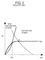
- the operating point Q of the driving thin film transistor T2 generally exists in a saturation region as in the characteristic graph of a transistor in FIG. 3. This is because a stable current Id can be supplied to the EL cell OLED even though the voltage Vds between the drain terminal and the source terminal of the driving thin film transistor T2 is changed. At this moment, the amount of change of the current Id flowing in the driving thin film transistor T2 in the saturation region is bigger than in the non-saturation region, for the deviation of the threshold voltage Vth of each of the driving thin film transistors T2.
- the EL display device of the prior art expresses the gray level by the change of the data voltage, thus in case that the threshold voltage Vth of the driving thin film transistor is not uniform for each line of the EL panel 20, the amount of the current flowing in the EL cell OLED cannot be accurately controlled (in fact, the current amount decreases) for the same data voltage, thus there is a problem that a desired picture is not displayed because the brightness is not uniform.
- an object of the present invention to provide an electro-luminescence display device that is adaptive for preventing picture quality deterioration by operating a thin film transistor for an electro-luminescence cell drive at a non-saturation area to compensate a threshold voltage, and a driving method thereof.
- an electro-luminescence display device includes an electro-luminescence cell connected between a first supply voltage source and a ground voltage source to emit light by a current supplied from the first supply voltage source; a cell driver formed every intersection of gate lines and data lines and connected between the first supply voltage source and the electro-luminescence cell to control a current flowing in the pixel cell; and a pulse supplier supplies to the electro-luminescence cell a pulse amplitude modulation signal which is divided to have N (N is a natural number) numbers of different voltage levels from each other, and wherein the driving thin film transistor operates at the non-saturation region.
- the electro-luminescence display device further includes a data driver to supply to the data line an on/off signal which is to drive the driving thin film transistor; and a gate driver to supply a scan pulse to the gate line.
- the cell driver includes: a switching thin film transistor connected to the gate line, the data line and the driving thin film transistor, to supply the on/off signal on the data line to the gate terminal of the driving thin film transistor; and a storage capacitor connected between the gate terminal of the driving thin film transistor and the first supply voltage source.
- the data driver includes: a first resistor and a second resistor connected in series between a second supply voltage source and the ground voltage source; and a first switching device connected between the second resistor and the ground voltage source.
- the data driver supplies to the data line a voltage on a node between a first resistor and a second resistor in accordance with the switching of the first switching device and the on/off signal of high state or low state by a voltage difference from the first supply voltage source.
- N numbers of pulse signals corresponding to the bit number and having the same duty cycle are supplied to the gate terminal of the first switching device while a scan pulse is supplied to the gate line.
- Each of the n numbers of pulse signals has a read section of a first voltage level and a write section of a second voltage level which is different from the first voltage level.
- the pulse supplier supplies to a cathode terminal of the electro-luminescence cell the pulse amplitude modulation signal which is synchronized with the n numbers of pulse signals, has the same duty cycle and has n numbers of different voltage levels from each other.
- Each of the n numbers of pulse amplitude modulation signals has a read section which is the same as the voltage level from the first supply voltage source and a write section having different voltage levels between the voltage level of the read section and a ground voltage from the ground voltage source.
- the driving thin film transistor operates at the non-saturation region by a voltage difference between the drain-source caused by a voltage supplied to the write section of the n numbers of pulse amplitude modulation signals in relation to a voltage between fixed gate and source terminals.
- the electro-luminescence cell emits light by a voltage level of a write section of each of the n numbers of pulse amplitude modulation signal and the current corresponding to a voltage difference with the first supply voltage source, and expresses a gray level corresponding to the N bit by the sum of the n numbers of the light-emitting brightness.
- a driving method of an electro-luminescence display device having a cell driver inclusive of an electro-luminescence cell which is connected between a first supply voltage source and a ground voltage source to emit light by a current supplied from the first supply voltage source and a driving thin film transistor which is formed at each intersection of gate lines and data lines and connected between the first supply voltage source and the electro-luminescence cell to control a current flowing in the pixel cell, according to another aspect of the present invention includes the steps of: supplying to the electro-luminescence cell a pulse amplitude modulation signal which is divided to have n (n is a natural number) numbers of different voltage levels from one another; and operating the driving thin film transistor at a non-saturation region by the pulse amplitude modulation signal.
- the driving method further includes the steps of: generating an on/off signal to drive the driving thin film transistor; and supplying a scan pulse to the gate line.
- the step of generating the on/off signal includes: generating n numbers of pulse signals that correspond to the bit number of a digital data and have the same duty cycle while a scan pulse is supplied to the gate line; and generating the on/off signal of high state and low state by use of the pulse signal.
- Each of the n number of pulse signals has a read section of a first voltage level and a write section of a second voltage level that is different from the first voltage level.
- the pulse amplitude modulation signal is supplied to a cathode terminal of the electro-luminescence cell, is synchronized with the pulse signal, has the same duty cycle and has the n numbers of different voltage levels from each other.
- Each of the n numbers of pulse amplitude modulation signals has the same read section as a voltage level from the first supply voltage source, and a write section having a different voltage level from each other between the voltage level of the read section and a ground voltage from the ground voltage source.
- the driving thin film transistor operates at the non-saturation region by a voltage difference between the drain and the source by the voltage supplied to the write section of the n numbers of pulse amplitude modulation signal in relation to a voltage between the gate and the source which are fixed.
- the electro-luminescence cell emits light by the current corresponding to a voltage difference between the first supply voltage source and a voltage level of a write section of each of the n numbers of pulse amplitude modulation signals, and expresses a gray level corresponding to the n bit by the sum of the light-emitting brightness of each of the n numbers.
- An electro-luminescence display device includes an electro-luminescence cell connected between a first supply voltage source and a ground voltage source to emit light by a current supplied from the first supply voltage source; and a cell driver formed at each intersection of gate lines and data lines and connected between the first supply voltage source and the electro-luminescence cell to control a current flowing in the pixel cell, and wherein the driving thin film transistor operates at a non-saturation region.
- the electro-luminescence display device further includes: a data driver to supply to the data line an on/off signal which is for driving the driving thin film transistor; a gate driver to supply a scan pulse to the gate line; and a pulse supplier to supply a pulse width modulation signal to the electro-luminescence cell.
- the cell driver includes: a switching thin film transistor connected to the gate line and the data line and the driving thin film transistor to supply an on/off signal on the data line to a gate terminal of the driving thin film transistor in response to the scan pulse; and a storage capacitor connected between a gate terminal of the driving thin film transistor and the first supply voltage source.
- the data driver includes: a first resistor and a second resistor connected in series between a second supply voltage source and the ground voltage source; a first switching device connected between the second resistor and the ground voltage source.
- the data driver supplies to the data line the on/off signal of high state or low state by a voltage difference between the first supply voltage source and a voltage on a node between a first resistor and a second resistor in accordance with the switching of the first switching device.
- a modulation data signal having a duty cycle corresponding to the bit number of a digital data and being divided into n steps (n is a natural number) is supplied to a gate terminal of the first switching device while a scan pulse is supplied to the gate line.
- a modulation data signal of each of the n steps has a read section of a first voltage level and a write section of a second voltage level which is different from the first voltage level.
- the pulse supplier supplies to a cathode terminal of the electro-luminescence cell the pulse width modulation signal which is synchronized with the modulation data signal, has the same duty cycle and is divided into the n steps.
- the pulse width modulation signal of each of the n steps has the same read section as a voltage level from the first supply voltage source, and a write section having a level between a ground voltage from the ground voltage source and a voltage level of the read section.
- the driving thin film transistor operates at the non-saturation region by a voltage difference between a drain and a source caused by a voltage supplied in a write section of a pulse width modulation signal of each of the n steps in relation to a voltage of a gate and a source which are fixed.
- the electro-luminescence cell emits light by the current caused by a voltage difference between the first supply voltage source and a voltage level of a write section of each of the n steps of pulse width modulation signals, and expresses a gray level corresponding to the n bit by the sum of a light-emitting time of each of the n step.
- the data driver further includes: a third resistor connected between the second supply voltage source and a node between the first and the second resistors; and a second switching device connected between the third resistor and the second supply voltage source and connects the third resistor in parallel to the first resistor in response to a mode selection signal supplied from the outside.
- the data driver supplies to the data line the on/off signal of low state having a first level or high state by a voltage difference between the first supply voltage source and a voltage on a node between a first resistor and a second resistor in accordance with the switching of the first switching device in case the second switching device is turned off by the mode selection signal, and supplies to the data line the on/off signal of low state having a second level or high state by a voltage difference between the first supply voltage source and a voltage on a node between the second resistor and a parallel resistor of the first and second resistors in accordance with the switching of the first switching device in case the second switching device is turned on by the mode selection signal.
- the driving thin film transistor has first and second voltages between gate and source which are different in accordance with the on/off signal of low state having the first and second levels.
- the driving thin film transistor controls the size of a current flowing in the electro-luminescence cell in 2 levels in accordance with the first and second voltages between gate and source.
- the driving method further includes the steps of: generating an on/off signal to drive the driving thin film transistor; supplying a scan pulse to the gate line; and supplying a pulse width modulation signal to the electro-luminescence cell.
- the step of generating the on/off signal includes: generating a modulation data signal which has a duty cycle corresponding to the bit number of a digital data and is divided into n steps (n is a natural number) while a scan pulse is supplied to the gate line; and generating the on/off signal of high state and low state by use of the modulation data signal.
- Each of the modulation data signal of the n step has a read section of a first voltage level and a write section of a second voltage level that is different from the first voltage level.
- the pulse width modulation signal is synchronized with the modulation data signal, has the same duty cycle, is divided into the n steps, and is supplied to a cathode terminal of the electro-luminescence cell.
- Each of the pulse width modulation signals of n step has the same read section as a voltage level from the first supply voltage source, and a write section having a level between the voltage level of the read section and a ground voltage from the ground voltage source.
- the driving thin film transistor operates at the non-saturation region by a voltage difference between the drain and the source by the voltage supplied to the write section of each of the pulse width modulation signal of n step in relation to a voltage between the gate and the source which are fixed.
- the electro-luminescence cell emits light by the current caused by the voltage difference between the first supply voltage source and a voltage level of a write section of each of the pulse width modulation signals of n step, and expresses a gray level corresponding to the n bit by the sum of the light-emitting time of each of the n steps.
- the step of generating the on/off signal includes: generating the on/off signal of low state having a first level or high state by a mode selection signal; and generating the on/off signal of low state having a second level of high state by the mode selection signal.
- the driving thin film transistor has first and second voltages between gate and source which are different from each other, in accordance with the on/off signal of low state having the first and second levels.
- the driving thin film transistor controls the size of a current flowing in the electro-luminescence cell in 2 levels in accordance with the first and second voltages between gate and source.
- FIG. 1 is a block diagram illustrating an electro- luminescence display device of the prior art
- FIG. 2 is a circuit diagram illustrating a pixel cell shown in FIG. 1;
- FIG. 3 is a diagram representing the operation characteristic of a driving thin film transistor shown in FIG. 2;
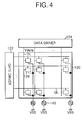
- FIG. 4 is a block diagram representing an electro- luminescence display device according to an embodiment of the present invention.
- FIG. 5 is a circuit diagram illustrating a pixel cell, a data driver and a pulse supplier of the electro-luminescence display device according to the first embodiment of the present invention shown in FIG. 4;
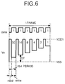
- FIG. 6 is a waveform diagram illustrating a pulse amplitude modulation signal supplied to the cathode electrode of an EL cell and a pulse signal supplied to a switching device shown in FIG. 5;
- FIG. 7 is a diagram illustrating the operation characteristic of a driving thin film transistor according to the first embodiment of the present invention shown in FIG. 5;
- FIG. 8 is a drive waveform diagram for expressing forty eight gray levels in a pixel cell shown in FIG. 5;
- FIG. 9 is a waveform diagram illustrating a pulse amplitude modulation signal supplied to the cathode electrode of an EL cell and a modulation data signal according to a second embodiment of the present invention.
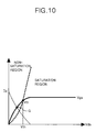
- FIG. 10 is a diagram illustrating the operation characteristic of a driving thin film transistor according to the second embodiment of the present invention.
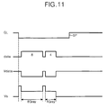
- FIG. 11 is a drive waveform diagram for expressing twelve gray levels in a pixel cell shown in FIG. 5;
- FIG. 12 is a circuit diagram illustrating a pixel cell, a data driver and a pulse supplier of the electro-luminescence display device according to the third embodiment of the present invention.
- FIG. 13 is a diagram illustrating the operation characteristic of a driving thin film transistor according to the third embodiment of the present invention shown in FIG. 12.
- an electro-luminescence (hereinafter, referred to as EL) according to a first embodiment of the present invention includes an EL panel 120 having pixel cells 128, inclusive of EL cells OLED and a driving thin film transistor T2 to drive the EL cell OLED, arranged at areas defined by intersections between gate lines GL and data lines DL; a gate driver 122 to drive the gate lines GL of the EL panel 120; a data driver 124 to supply an on/off signal Vdata, which is for driving the pixel cells 128 of the EL panel 120, to the data lines DL; and a pulse supplier 140 to supply a pulse amplitude modulation signal Vs to a cathode electrode of the EL cell OLED, so that the driving thin film transistor T2 is made to operate at the non-saturation region.
- EL electro-luminescence
- the gate driver 122 supplies a scan pulse to the gate lines GL to sequentially drive the gate lines GL.
- Each of the pixel cells 128 receives an on/off signal Vdata from the data line DL when a scan pulse is supplied to the gate line GL, to generate a light corresponding to a pulse amplitude modulation signal Vs supplied from the pulse supplier 140.
- each of the pixels 128, as shown in FIG. 5, includes an EL cell OLED connected between a first supply voltage source VDD1 and the pulse supplier 140, and a cell driver 130 to drive the EL cell OLED.
- the cell driver 130 includes a switching thin film transistor T1, of which a gate terminal is connected to the gate line GL, a source terminal is connected to the data line DL and a drain terminal is connected to a first node N1; a driving thin film transistor T2, of which a gate terminal is connected to the first node N1, a drain terminal is connected to the first supply voltage source VDD1 and a source terminal is connected to an anode of the EL cell OLED; and a storage capacitor Cst connected between the first supply voltage source VDD1 and the first node N1.
- the switching thin film transistor T1 supplies the on/off signal Vdata, which is supplied to the data line DL by being turned on when a scan pulse is supplied to the gate line GL, to the first node N1.
- the on/off signal Vdata supplied to the first node N1 is charged into the storage capacitor Cst as well as being supplied to the gate terminal of the driving thin film transistor T2.
- the driving thin film transistor T2 is turned on/off in accordance with the on/off signal Vdata supplied to the gate terminal, to control the current amount Id, which is supplied from the first supply voltage source VDD1 through the EL cell OLED. And, even the switching thin film transistor T1 is turned off, the driving thin film transistor T2 remains at the on-state by the on/off signal Vdata charged in the storage capacitor Cst.
- the EL cell OLED receives, while the driving thin film transistor T2 is turned on, a pulse amplitude modulation signal Vs supplied to the cathode electrode of itself from the pulse supplier 140 and a current corresponding to the voltage difference from the first supply voltage VDD1 to emit light for a period when it corresponds to the pulse amplitude modulation signal Vs.
- the data driver 124 includes a data modulation circuit (not shown) which modulates the digital data inputted from the outside to n (n is a natural number) numbers of pulses corresponding to the bit number; a first resistor and a second resistor R1, R2 connected in series between the second supply voltage source VDD2 and the ground voltage source VSS; and a switch device SW connected between the second resistor R2 and the ground voltage source VSS.
- the second supply voltage source VDD2 has smaller voltage levels than the first supply voltage source VDD1.
- the data modulation circuit modulates the digital data inputted from the outside to n numbers of pulses having the same duty cycle in accordance with the bit number to supply it to the gate terminal of the switching device SW.
- the pulse signal data as shown in FIG. 6, while the scan pulse is supplied to the gate line GL, is supplied by being divided into 6 steps to have the same duty cycle in accordance with the digital value 0 to 63 corresponding to 6 bit.
- each step of the pulse signal data is divided into a read section for having the switching device SW off, and a write section for having the switching device SW on.
- the node between the first and second resistors R1, R2 is connected to the data line DL.
- the switching device SW selectively connects the second resistor R2 to the ground voltage source VSS in accordance with the pulse signal supplied from the data modulation circuit.
- the data driver 124 supplies the voltage from the second supply voltage source VDD2, i.e., the on/off signal Vdata of high state, to the data line DL through the first resistor R1 by having the switching device SW off by way of the read section of the pulse signal data supplied from the switching device SW.
- the data driver 124 connects the second resistor R2 to the ground voltage source VSS by having the switching device SW on by way of the write section of the pulse signal data supplied from the switching device SW. Due to this, the on/off signal Vdata of low state is supplied to the data line DL connected to the node between the first and second resistors R1, R2.
- the gate terminal of the driving thin film transistor T2 is connected to the ground voltage source VSS through the switching thin film transistor T1, the data line DL, the second resistor R2 of the data driver 124 and the switching device SW, thus in case that the switching device SW is the data driver 124 is on, the ground voltage, i.e., the on/off signal Vdata of low state, is supplied to the gate terminal of the driving thin film transistor T2 by the voltage difference between the first supply voltage source VDD1 and the voltage on the node between the first resistor R1 and the second resistor R2.
- the pulse supplier 140 is connected between the cathode electrode of the EL cell OLED and the ground voltage source VSS.
- the pulse supplier 140 supplies the pulse amplitude modulation signal Vs to the cathode electrode of the EL cell OLED, wherein the pulse amplitude modulation signal Vs is synchronized with each step of the pulse signal data supplied to the switching device SW of the data driver 124 and has the same duty cycle as well as having the voltage levels of n steps corresponding to the bit number of the digital data.
- the voltage level supplied to the cathode electrode of the EL cell OLED in the read section of the pulse amplitude modulation signal Vs has the same voltage level as the first supply voltage source VDD1, and the voltage supplied to the cathode of the EL cell OLED in the write section has the levels of n steps (32, 16, 8, 4, 2, 1) between the first supply voltage source VDD1 and the ground voltage source VSS.
- the voltage level between the ground voltage source and the first supply voltage source VDD1 supplied in the write section of the pulse amplitude modulation signal Vs while the voltage Vgs of the source terminal and the gate terminal of the driving thin film transistor T2 is fixed by the data driver 124, changes the voltage Vds of the source terminal and the drain terminal of the driving thin film transistor T2 to the level of n steps (32, 16, 8, 4, 2, 1), thus the operating point Q of the driving thin film transistor T2 is made to be in a non-saturation region as shown in FIG. 7.
- the EL display device and the driving method thereof according to the first embodiment of the present invention has the operation point Q of the driving thin film transistor T2 in the non-saturation region, thus the change amount of the current Id flowing in the driving thin film transistor T2 by the deviation of the threshold voltage Vth can be made smaller than the prior art in relation to the fixed Vgs supplied from the data driver 124.
- the EL display device and the driving method thereof according to the first embodiment of the present invention can prevent picture quality deterioration by compensating the deviation of the threshold voltage Vth of the driving thin film transistor T2.
- the EL cell OLED receives the voltage from the first supply voltage source VDD1 supplied through the driving thin film transistor T2 and the current from the first supply voltage source VDD1 by the voltage difference DT from the pulse supplier 140, thereby emitting light. Accordingly, the EL cell OLED expresses the gray level corresponding to the bit number of the digital data by the sum of the light-emitting brightness of n step by the pulse amplitude modulation signal supplied step by step from the pulse supplier 140 so as to be synchronized with the on/of signal Vdata supplied by steps from the data driver 124 during the period when the scan pulse is supplied to the gate line GL.
- the data driver 124 sequentially supplies the pulse signal of first step corresponding to the digital data (100000) of 32 and the pulse signal of second step corresponding to the digital data (010000) of 16 subsequent to the first step to the switching device SW while the scan pulse SP is supplied to the gate line GL.
- the switching device SW sequentially supplies the on/off signal Vdata to the gate terminal of the driving thin film transistor T2 through the switching thin film transistor T1, in response to each of the pulse signals of the first and second steps sequentially supplied from the data driver 124, and at the same time the pulse amplitude modulation signal 32 of first step being synchronized with each of the pulse signals of the first and second steps from the pulse supplier 140 and having the voltage level corresponding to the digital data (100000) of 32 and the pulse amplitude modulation signal 16 of second step having the voltage level corresponding to the digital data (010000) of 16 are supplied step by step to the cathode electrode of the EL cell OLED.
- the driving thin film transistor T2 is turned on by the on/off signal Vdata sequentially supplied by the first and second steps, to control the current amount Id supplied from the first supply voltage source VDD1 through the EL cell OLED.
- the EL cell OLED receives the voltage levels (32, 16) of each of the pulse amplitude modulation signals (32, 16) of the first and second steps supplied to the cathode electrode of itself and the current corresponding to the voltage difference with the first supply voltage source VDD1 and is made to emit light step by step.
- the EL display device and the driving method thereof according to the first embodiment of the present invention has the EL cell OLED emit light by the first and second steps, thus the 48 gray levels are expressed by the sum of the light-emitting brightness 32 of the first step and the light-emitting brightness 16 of the second step.
- the second embodiment includes the contents of FIGs. 4 and 5 of the first embodiment as it is, thus it will be described in conjunction with FIGs. 4 and 5 without separate drawings.
- FIG. 9 is a waveform diagram representing a modulation data signal supplied to a switching device and a pulse width modulation signal supplied to the cathode electrode of the EL cell, shown in FIG. 5.
- FIG. 10 is a diagram illustrating an operation characteristic of a driving thin film transistor.
- FIG. 11 is a drive waveform diagram for expressing 12 gray levels in a pixel cell shown in FIG. 5.
- an electro-luminescence (hereinafter, referred to as EL) according to a second embodiment of the present invention includes an EL panel 120 having pixel cells 128, inclusive of EL cells OLED and a driving thin film transistor T2 to drive the EL cell OLED, arranged at areas defined by intersections between gate lines GL and data lines DL; a gate driver 122 to drive the gate lines GL of the EL panel 120; a data driver 124 to supply an on/off signal Vdata, which is for driving the pixel cells 128 of the EL panel 120, to the data lines DL; and a pulse supplier 140 to supply a pulse width modulation signal Vs to a cathode electrode of the EL cell OLED, so that the driving thin film transistor T2 is made to operate at the non-saturation region.
- EL electro-luminescence
- the gate driver 122 supplies a scan pulse to the gate lines GL to sequentially drive the gate lines GL.
- Each of the pixel cells 128 receives an on/off signal Vdata from the data line DL when a scan pulse is supplied to the gate line GL, to generate a light corresponding to a pulse width modulation signal Vs supplied from the pulse supplier 140.
- each of the pixels 128, as shown in FIG. 5, includes an EL cell OLED connected between a first supply voltage source VDD1 and the pulse supplier 140, and a cell driver 130 to drive the EL cell OLED.
- the cell driver 130 includes a switching thin film transistor T1, of which a gate terminal is connected to the gate line GL, a source terminal is connected to the data line DL and a drain terminal is connected to a first node N1; a driving thin film transistor T2, of which a gate terminal is connected to the first node N1, a drain terminal is connected to the first supply voltage source VDD1 and a source terminal is connected to an anode of the EL cell OLED; and a storage capacitor Cst connected between the first supply voltage source VDD1 and the first node N1.
- the switching thin film transistor T1 supplies the on/off signal Vdata, which is supplied to the data line DL by being turned on when a scan pulse is supplied to the gate line GL, to the first node N1.
- the on/off signal Vdata supplied to the first node N1 is charged into the storage capacitor Cst as well as being supplied to the gate terminal of the driving thin film transistor T2.
- the driving thin film transistor T2 is turned on/off in accordance with the on/off signal Vdata supplied to the gate terminal, to control the current amount Id, which is supplied from the first supply voltage source VDD1 through the EL cell OLED. And, even the switching thin film transistor T1 is turned off, the driving thin film transistor T2 remains at the on-state by the on/off signal Vdata charged in the storage capacitor Cst.
- the EL cell OLED receives, while the driving thin film transistor T2 is turned on, a pulse width modulation signal Vs supplied to the cathode electrode of itself from the pulse supplier 140 and a current corresponding to the voltage difference from the first supply voltage VDD1 to emit light for a period when it corresponds to the pulse width modulation signal Vs.
- the data driver 124 includes a data modulation circuit (not shown) which modulates it to have a duty cycle of n step (n is a natural number) corresponding to the bit number of the digital data inputted from the outside; a first resistor and a second resistor R1, R2 connected in series between the second supply voltage source VDD2 and the ground voltage source VSS; and a switch device SW connected between the second resistor R2 and the ground voltage source VSS.
- the second supply voltage source VDD2 has smaller voltage levels than the first supply voltage source VDD1.
- the data modulation circuit modulates the digital data inputted from the outside to have the duty cycle of n step corresponding to the bit number to supply it to the gate terminal of the switching device SW.
- the modulation data signal data as shown in FIG. 9, while the scan pulse is supplied to the gate line GL, is supplied by being divided to have the duty cycle of 4 step (8, 4, 2, 1) in accordance with the digital value 0 to 15 corresponding to 4 bit.
- each step of the modulation data signal data is divided into a read section for having the switching device SW off, and a write section for having the switching device SW on.
- the 16 gray levels are expressed by the sum of the gray levels expressed by the 4 step (8, 4, 2, 1) of the modulation data signal data.
- the first step expresses 8 gray levels
- the second step expresses 4 gray levels
- the third step expresses 2 gray levels
- the fourth step expresses 1 gray level.
- the node between the first and second resistors R1, R2 is connected to the data line DL.
- the switching device SW selectively connects the second resistor R2 to the ground voltage source VSS in accordance with the modulation data signal data supplied from the data modulation circuit.
- the data driver 124 supplies the voltage from the second supply voltage source VDD2, i.e., the on/off signal Vdata of high state, to the data line DL through the first resistor R1 by having the switching device SW off by way of the read section of the modulation data signal data supplied from the switching device SW.
- the data driver 124 connects the second resistor R2 to the ground voltage source VSS by having the switching device SW on by way of the write section of the modulation data signal data supplied from the switching device SW. Due to this, the on/off signal Vdata of low state is supplied to the data line DL connected to the node between the first and second resistors R1, R2.
- the gate terminal of the driving thin film transistor T2 is connected to the ground voltage source VSS through the switching thin film transistor T1, the data line DL, the second resistor R2 of the data driver 124 and the switching device SW, thus in case that the switching device SW is the data driver 124 is on, the ground voltage, i.e., the on/off signal Vdata of low state, is supplied to the gate terminal of the driving thin film transistor T2 by the voltage difference between the first supply voltage source VDD1 and the voltage on the node between the first resistor R1 and the second resistor R2.
- the pulse supplier 140 is connected between the cathode electrode of the EL cell OLED and the ground voltage source VSS.
- the pulse supplier 140 supplies the pulse width modulation signal Vs to the cathode electrode of the EL cell OLED, wherein the pulse width modulation signal Vs is synchronized with each step of the modulation data signal data supplied to the switching device SW of the data driver 124 and has the same duty cycle.
- the voltage level supplied to the cathode electrode of the EL cell OLED in the read section of the pulse width modulation signal Vs has the same voltage level as the first supply voltage source VDD1, and the voltage level supplied to the cathode of the EL cell OLED in the write section has the voltage level between the first supply voltage source VDD1 and the ground voltage source VSS.
- the EL display device and the driving method thereof according to the second embodiment of the present invention has the operation point Q of the driving thin film transistor T2 in the non-saturation region, thus the change amount of the current Id flowing in the driving thin film transistor T2 by the deviation of the threshold voltage Vth can be made smaller than the prior art in relation to the fixed Vgs supplied from the data driver 124.
- the EL display device and the driving method thereof according to the second embodiment of the present invention can prevent picture quality deterioration by compensating the deviation of the threshold voltage Vth of the driving thin film transistor T2.
- the EL cell OLED receives the voltage from the first supply voltage source VDD1 supplied through the driving thin film transistor T2 and the current from the first supply voltage source VDD1 by the voltage difference DT from the pulse supplier 140, thereby emitting light. Accordingly, the EL cell OLED expresses the gray level corresponding to the bit number of the digital data by the sum of the light-emitting time of n step by the pulse width modulation signal supplied step by step from the pulse supplier 140 so as to be synchronized with the on/of signal Vdata supplied by steps from the data driver 124 during the period when the scan pulse is supplied to the gate line GL.
- the data driver 124 sequentially supplies the modulation data signal (8) of first step having the duty cycle corresponding to the digital data (1000) of 8 and the modulation data signal (4) of second step having the duty cycle corresponding to the digital data (0100) of 4 subsequent to the first step to the switching device SW while the scan pulse SP is supplied to the gate line GL.
- the switching device SW sequentially supplies the on/off signal Vdata to the gate terminal of the driving thin film transistor T2 through the switching thin film transistor T1, in response to each of the modulation data signals (8, 4) of the first and second steps sequentially supplied from the data driver 124, and at the same time the pulse width modulation signal Vs of first and second steps being synchronized with each of the modulation data signals (8, 4) of the first and second steps from the pulse supplier 140 and having the same duty cycle are supplied step by step to the cathode electrode of the EL cell OLED.
- the driving thin film transistor T2 is turned on by the on/off signal Vdata sequentially supplied by the first and second steps, to control the current amount Id supplied from the first supply voltage source VDD1 through the EL cell OLED.
- the EL cell OLED emits light for the duty cycle of each of the pulse width modulation signals Vs of the first and second steps supplied to the cathode electrode of itself.
- the EL display device and the driving method thereof according to the second embodiment of the present invention has the EL cell OLED emit light by the first and second steps while the scan pulse SP is supplied to the gate line GL, thus 12 gray levels are expressed by the sum of 8 gray levels by the light-emitting time of the first step and 4 gray levels by the light-emitting time of the second step.
- an EL display device is the same as the EL display device according to the second embodiment of the present invention except the data driver 224. Accordingly, in the EL display device according to the third embodiment of the present invention, the description of the EL display device according to the second embodiment of the present invention will substitute for the description for the components except the data driver 224.
- the EL display device controls the brightness of the EL panel 120 in accordance with the mode selection signal MD.
- the mode selection signal MD becomes high state in case of bright mode, and the mode selection signal MD becomes low state in case of dark mode.
- the data driver 224 of the EL display device includes a data modulation circuit (not shown) to modulate the digital data inputted from the outside to have a duty cycle of n step (n is a natural number) corresponding to the bit number, a first resistor and a second resistor R1, R2 connected in series between the second supply voltage source VDD2 and the ground voltage source VSS, a first switching device SW1 connected between the second resistor R2 and the ground voltage source VSS, a second switching device SW2 connected between the second supply voltage source VDD2 and a node between the first resistor R1 and the second resistor R2, and a third resistor R3 connected between the second switching device SW2 and a node between the first resistor R1 and the second resistor R2.
- the data modulation circuit modulates the digital data inputted from the outside to have the duty cycle of n step corresponding to the bit number, and supplies it to the gate terminal of the switching device SW.
- the modulation data signal data is supplied by being divided to have the duty cycle of 4 steps (8, 4, 2, 1) in accordance with the digital value 0 to 15 corresponding to the 4 bit while the scan signal is supplied to the gate line GL.
- each step of the modulation data signal data is divided into a read section for having the switching device SW off and a write section for having the switching device SW on.
- the 16 gray levels are expressed by the sum of the gray levels expressed by the 4 step (8, 4, 2, 1) of the modulation data signal data.
- the first step expresses 8 gray levels
- the second step expresses 4 gray levels
- the third step expresses 2 gray levels
- the fourth step expresses 1 gray level.
- the node between the first and second resistors R1, R2 is connected to the data line DL.
- the third resistor R3 is selectively connected in parallel to the first resistor R1 in accordance with the switching of the second switching device SW2.
- the first switching device SW1 selectively connects the second resistor R2 to the ground voltage source VSS in accordance with the modulation data signal data supplied from the data modulation circuit.
- the second switching device SW2 is switched by an inputted mode selection signal MD to selectively connects the third resistor R3 in parallel to the first resistor R1.
- the data driver 224 turns off the first switching device SW1 by the read section of the modulation data signal data supplied to the first switching device SW1 to supply the voltage from the second supply voltage source VDD2, i.e., the on/off signal Vdata of high state, to the data line DL through the first resistor R1.
- the data driver 224 turns on the first switching device SW1 by the write section of the modulation data signal data supplied to the first switching device SW1 when the second switching device SW2 is turned off by the mode selection signal MD of high state, thereby connecting the second resistor R2 to the ground voltage source VSS. Because of this, the on/off signal Vdata of low state having the first step is supplied to the data line DL connected to the node between the first and second resistors R1, R2.
- the gate terminal of the driving thin film transistor T2 is connected to the ground voltage source VSS through the switching thin film transistor T1, the data line DL, the second resistor R2 of the data driver 224 and the first switching device SW1 when the scan pulse is supplied to the gate line GL, thus the ground voltage, i.e., the on/off signal Vdata of low state having the first level is supplied to the gate terminal of the driving thin film transistor T2 by the voltage difference between the first voltage source VDD1 and the voltage on the node between the first resistor R1 and the second resistor R2 when the first switching device SW1 of the data driver 224 is turned on.
- the data driver 224 turns on the first switching device SW1 by the write section of the modulation data signal data supplied to the first switching device SW1 when the second switching device SW2 is turned on by the mode selection signal MD of low state, thereby connecting the second resistor R2 to the ground voltage source VSS and in addition connects the third resistor R3 to the first resistor R1 in parallel by the second switching device SW2. Because of this, the on/off signal Vdata of low state having the second level different from the first level is supplied to the data line DL connected to the node between the first and second resistors R1, R2.
- the gate terminal of the driving thin film transistor T2 is connected to the ground voltage source VSS through the switching thin film transistor T1, the data line DL, the second resistor R2 of the data driver 224 and the first switching device SW1 when the scan pulse is supplied to the gate line GL, thus the ground voltage, i.e., the on/off signal Vdata of low state having the second level is supplied to the gate terminal of the driving thin film transistor T2 by the voltage difference between the first voltage source VDD1 and the voltage on the node between the second resistor R2 and the parallel resistor of the first resistor R1 and the third resistor R3 when the first switching device SW1 of the data driver 224 is turned on.
- the EL display device and the driving method thereof according to the third embodiment of the present invention selectively supplies the on/off signal Vdata of low state having the first and second levels to the gate terminal of the driving thin film transistor T2 of the pixel cell 128 in accordance with the mode selection signal MD, thereby enabling to make the voltage Vgs of the gate terminal and the source terminal of the driving thin film transistor T2 changed to two levels Vgs1, Vgs2 as shown in FIG. 13.
- the EL display device and the driving method thereof supplies the pulse width modulation signal Vs having the duty cycle of n step in accordance with the digital data to the cathode electrode of the EL cell OLED as described in the first embodiment of the present invention, thus the voltage Vds of the drain terminal and the source terminal of the driving thin film transistor T2 is made to be small while the voltage Vgs of the gate terminal and the source terminal of the thin film transistor T2 is fixed to two levels Vgs1, Vgs2, thereby enabling the operation points Q1, Q2 of the driving thin film transistor T2 to be in the non-saturation region as shown in FIG. 13.
- the EL display device and the driving method thereof according to the third embodiment of the present invention can make the change amount of the current Id flowing in the drivin thin film transistor T2 caused by the deviation of the threshold voltage Vth smaller than the prior art, in relation to the fixed Vgs1, Vgs2 supplied from the data driver 224 in accordance with the mode selection signal MD since the operation points Q1, Q2 of the driving thin film transistor T2 exist in the non-saturation region.
- the EL display device and the driving method thereof according to the third embodiment of the present invention might prevent picture quality deterioration by compensating the deviation of the threshold voltage Vth of the driving thin film transistor T2.
- the data driver 224 sequentially supplies the modulation data signal (8) of first step having the duty cycle corresponding to the fact that the digital data value is 8 and the modulation data signal (4) of second step having the duty cycle corresponding to the fact that the digital value is 4, subsequent to the first step to the first switching device SW1 while the scan pulse SP is supplied to the gate line GL.
- the first switching device SW1 sequentially supplies the on/off signal Vdata of low state having any one level of the first and second levels according to the mode selection signal MD to the gate terminal of the driving thin film transistor T2 through the switching thin film transistor T1, in response to each of the modulation data signals (8, 4) of the first and second steps sequentially supplied from the data driver 224, and at the same time the pulse width modulation signal Vs of first and second steps being synchronized with each of the modulation data signals (8, 4) of the first and second steps from the pulse supplier 140 and having the same duty cycle are supplied step by step to the cathode electrode of the EL cell OLED.
- the driving thin film transistor T2 is turned on by the on/off signal Vdata of low state, having any one level of the first and second levels, sequentially supplied by the first and second steps, to control the size of the current amount Id supplied from the first supply voltage source VDD1 through the EL cell OLED.
- the EL cell OLED emits light for the duty cycle of each of the pulse width modulation signals Vs of the first and second steps supplied to the cathode electrode of itself.
- the EL display device and the driving method thereof according to the third embodiment of the present invention has the EL cell OLED emit light by the first and second steps while the scan pulse SP is supplied to the gate line GL, thus 12 gray levels are expressed by the sum of 8 gray levels by the light-emitting time of the first step and 4 gray levels by the light-emitting time of the second step.
- the 12 gray levels expressed by the EL display panel and the driving method thereof according to the third embodiment of the present invention are expressed as the bright 12 gray levels or the dark 12 gray levels in accordance with the mode selection signal MD.
- the electro-luminescence display device and the driving method thereof supplies the on/off signal of high or low state to the driving thin film transistor of the pixel cell to drive, and at the same time supplies the pulse amplitude modulation signal to the cathode electrode of the EL cell to control the light-emission brightness of the EL cell by steps so that the desired gray level is expressed by the sum of the light-emitting brightness by steps, thus the voltage between the drain and source terminals is made to be small in relation to the voltage between the gate and source of the fixed driving thin film transistor to make the driving thin film transistor operate at the non-saturation region.
- the present invention reduces the deviation of the threshold voltage generated between the driving thin film transistors due to the non-uniformity of the excimer laser illuminated upon the formation of the driving thin film transistor, thereby preventing the picture quality deterioration by the deviation of the threshold voltage.
- the electro-luminescence display device and the driving method thereof controls the size of the current flowing in the EL cell in accordance with the mode selection signal, and at the same time, supplies the pulse width modulation signal to the cathode electrode of the EL cell to express the gray level by the sum of the light-emitting time of the EL cell and the light-emitting time by the control, thereby operating the driving thin film transistor at the non-saturation region by making the voltage between the drain and source terminals small in relation to the voltage between the gate-source terminals of the fixed driving thin film transistor.
- the present invention reduces the deviation of the threshold voltage generated between the driving thin film transistors caused by the non-uniformity of the excimer laser illuminated when forming the driving thin film transistors, thus the picture quality deviation caused by the deviation of the threshold voltage might be prevented and the entire brightness of the electro- luminescence panel might be able to be controlled in two modes in accordance with the mode selection signal.
Landscapes
- Engineering & Computer Science (AREA)
- Physics & Mathematics (AREA)
- Computer Hardware Design (AREA)
- General Physics & Mathematics (AREA)
- Theoretical Computer Science (AREA)
- Electroluminescent Light Sources (AREA)
- Control Of El Displays (AREA)
- Control Of Indicators Other Than Cathode Ray Tubes (AREA)
- Analogue/Digital Conversion (AREA)
- Electronic Switches (AREA)
Applications Claiming Priority (4)
| Application Number | Priority Date | Filing Date | Title |
|---|---|---|---|
| KR2004006880 | 2004-02-03 | ||
| KR1020040006880A KR100692862B1 (ko) | 2004-02-03 | 2004-02-03 | 일렉트로-루미네센스 표시장치와 그의 구동방법 |
| KR2004006879 | 2004-02-03 | ||
| KR1020040006879A KR100606411B1 (ko) | 2004-02-03 | 2004-02-03 | 일렉트로-루미네센스 표시장치와 그의 구동방법 |
Publications (2)
| Publication Number | Publication Date |
|---|---|
| EP1562168A2 true EP1562168A2 (de) | 2005-08-10 |
| EP1562168A3 EP1562168A3 (de) | 2006-07-19 |
Family
ID=34680743
Family Applications (1)
| Application Number | Title | Priority Date | Filing Date |
|---|---|---|---|
| EP05002000A Withdrawn EP1562168A3 (de) | 2004-02-03 | 2005-02-01 | Elektrolumineszente Anzeigevorrichtung und Ansteuerverfahren dafür |
Country Status (4)
| Country | Link |
|---|---|
| US (1) | US7663589B2 (de) |
| EP (1) | EP1562168A3 (de) |
| JP (1) | JP5218879B2 (de) |
| CN (1) | CN1658264B (de) |
Cited By (1)
| Publication number | Priority date | Publication date | Assignee | Title |
|---|---|---|---|---|
| WO2012049000A1 (fr) * | 2010-10-15 | 2012-04-19 | Commissariat A L'energie Atomique Et Aux Energies Alternatives | Ecran d'affichage a diodes electroluminescentes a matrice active pourvu de moyens d'attenuation |
Families Citing this family (32)
| Publication number | Priority date | Publication date | Assignee | Title |
|---|---|---|---|---|
| JP2007086347A (ja) * | 2005-09-21 | 2007-04-05 | Eastman Kodak Co | 表示装置 |
| KR100804639B1 (ko) * | 2005-11-28 | 2008-02-21 | 삼성전자주식회사 | 디스플레이 장치 구동 방법 |
| JP5538727B2 (ja) * | 2006-02-10 | 2014-07-02 | コーニンクレッカ フィリップス エヌ ヴェ | 大面積薄膜回路 |
| TW200741383A (en) * | 2006-03-29 | 2007-11-01 | Koninkl Philips Electronics Nv | Setup for storing data in a holographic storage medium |
| US7956831B2 (en) * | 2007-05-30 | 2011-06-07 | Honeywell Interntional Inc. | Apparatus, systems, and methods for dimming an active matrix light-emitting diode (LED) display |
| KR101534191B1 (ko) | 2008-10-15 | 2015-07-06 | 삼성전자주식회사 | 디스플레이 장치 및 그 구동 방법 |
| KR101441958B1 (ko) * | 2012-09-28 | 2014-09-18 | 엘지디스플레이 주식회사 | 박막트랜지스터 보상회로를 포함하는 액정표시장치 |
| TWI473062B (zh) * | 2013-01-22 | 2015-02-11 | Au Optronics Corp | 有機發光二極體顯示裝置及其驅動方法 |
| JP6079312B2 (ja) * | 2013-03-04 | 2017-02-15 | セイコーエプソン株式会社 | 電気光学装置、電子機器、及び電気光学装置の駆動方法 |
| US10839734B2 (en) * | 2013-12-23 | 2020-11-17 | Universal Display Corporation | OLED color tuning by driving mode variation |
| KR102072403B1 (ko) * | 2013-12-31 | 2020-02-03 | 엘지디스플레이 주식회사 | 하이브리드 구동 방식 유기발광표시장치 |
| TWI644592B (zh) * | 2015-07-03 | 2018-12-11 | 點晶科技股份有限公司 | 控制發光二極體亮度的信號產生方法及電路 |
| US9768238B2 (en) * | 2015-11-16 | 2017-09-19 | E I Du Pont De Nemours And Company | Electrical device to mask systematic luminance variation |
| US10102795B2 (en) * | 2016-06-06 | 2018-10-16 | Mikro Mesa Technology Co., Ltd. | Operating method of display device and display device |
| KR20180071896A (ko) * | 2016-12-20 | 2018-06-28 | 엘지디스플레이 주식회사 | 유기발광표시장치 및 그의 구동방법 |
| KR102390902B1 (ko) * | 2017-10-16 | 2022-04-25 | 엘지전자 주식회사 | 영상표시장치 |
| CN110556072B (zh) | 2018-05-31 | 2024-07-02 | 三星电子株式会社 | 显示面板以及显示面板的驱动方法 |
| EP3588479B1 (de) * | 2018-06-27 | 2021-08-04 | IMEC vzw | Digitale ansteuerungsimplementierung bei mehreren referenzlichtintensitäten |
| KR102538488B1 (ko) * | 2018-10-04 | 2023-06-01 | 삼성전자주식회사 | 디스플레이 패널 및 디스플레이 패널의 구동 방법 |
| KR102538484B1 (ko) | 2018-10-04 | 2023-06-01 | 삼성전자주식회사 | 디스플레이 패널 및 디스플레이 패널의 구동 방법 |
| DE102018131023B4 (de) * | 2018-12-05 | 2025-12-04 | OSRAM Opto Semiconductors Gesellschaft mit beschränkter Haftung | Optoelektronische leuchtvorrichtung mit einem pwm-transistor und verfahren zum herstellen oder steuern einer optoelektronischen leuchtvorrichtung |
| CN110021274B (zh) * | 2019-04-30 | 2021-03-23 | Tcl华星光电技术有限公司 | 显示面板驱动系统及显示面板驱动方法 |
| CN110264963A (zh) * | 2019-05-31 | 2019-09-20 | 深圳市华星光电半导体显示技术有限公司 | 一种发光元件的驱动方法及装置 |
| CN110047436B (zh) * | 2019-06-06 | 2021-11-23 | 京东方科技集团股份有限公司 | 像素电路、阵列基板、其驱动方法、显示面板及显示装置 |
| CN112071261A (zh) * | 2020-09-22 | 2020-12-11 | 禹创半导体(深圳)有限公司 | 一种micro LED的画素电路与驱动方法 |
| KR102738329B1 (ko) * | 2020-10-30 | 2024-12-04 | 엘지디스플레이 주식회사 | 표시패널과 이를 이용한 표시장치 |
| CN112419995B (zh) * | 2020-11-30 | 2022-07-08 | 成都中电熊猫显示科技有限公司 | 用于液晶显示装置的伽马驱动电路和液晶显示装置 |
| CN112863427B (zh) * | 2021-01-13 | 2022-05-13 | 厦门天马微电子有限公司 | 发光面板的亮度调节方法、发光面板及显示装置 |
| CN113113426A (zh) * | 2021-03-19 | 2021-07-13 | 武汉华星光电半导体显示技术有限公司 | 显示面板及其制备方法 |
| CN113053299B (zh) * | 2021-03-19 | 2022-10-11 | 京东方科技集团股份有限公司 | 像素驱动电路、像素驱动方法、显示面板及显示装置 |
| CN113053301B (zh) * | 2021-03-23 | 2022-08-19 | 京东方科技集团股份有限公司 | 像素驱动电路、像素驱动方法、显示面板及显示装置 |
| TWI863350B (zh) * | 2023-06-14 | 2024-11-21 | 希映顯示科技股份有限公司 | 穩態液晶顯示模組之改善干擾結構 |
Citations (1)
| Publication number | Priority date | Publication date | Assignee | Title |
|---|---|---|---|---|
| WO2003041042A1 (en) * | 2001-10-18 | 2003-05-15 | Samsung Electronics Co., Ltd. | An organic electroluminescence panel, a display with the same, and an apparatus and a method for driving thereof |
Family Cites Families (6)
| Publication number | Priority date | Publication date | Assignee | Title |
|---|---|---|---|---|
| US5748160A (en) * | 1995-08-21 | 1998-05-05 | Mororola, Inc. | Active driven LED matrices |
| JPH09218388A (ja) * | 1996-02-09 | 1997-08-19 | Hosiden Corp | 液晶表示装置 |
| JPH10319909A (ja) * | 1997-05-22 | 1998-12-04 | Casio Comput Co Ltd | 表示装置及びその駆動方法 |
| US5990629A (en) * | 1997-01-28 | 1999-11-23 | Casio Computer Co., Ltd. | Electroluminescent display device and a driving method thereof |
| KR100327375B1 (ko) * | 2000-03-06 | 2002-03-06 | 구자홍 | 액티브 구동 장치 |
| JP2003005710A (ja) | 2001-06-25 | 2003-01-08 | Nec Corp | 電流駆動回路及び画像表示装置 |
-
2005
- 2005-02-01 US US11/046,803 patent/US7663589B2/en active Active
- 2005-02-01 EP EP05002000A patent/EP1562168A3/de not_active Withdrawn
- 2005-02-03 JP JP2005027689A patent/JP5218879B2/ja not_active Expired - Fee Related
- 2005-02-03 CN CN200510006794.3A patent/CN1658264B/zh not_active Expired - Fee Related
Patent Citations (1)
| Publication number | Priority date | Publication date | Assignee | Title |
|---|---|---|---|---|
| WO2003041042A1 (en) * | 2001-10-18 | 2003-05-15 | Samsung Electronics Co., Ltd. | An organic electroluminescence panel, a display with the same, and an apparatus and a method for driving thereof |
Cited By (3)
| Publication number | Priority date | Publication date | Assignee | Title |
|---|---|---|---|---|
| WO2012049000A1 (fr) * | 2010-10-15 | 2012-04-19 | Commissariat A L'energie Atomique Et Aux Energies Alternatives | Ecran d'affichage a diodes electroluminescentes a matrice active pourvu de moyens d'attenuation |
| FR2966276A1 (fr) * | 2010-10-15 | 2012-04-20 | Commissariat Energie Atomique | Ecran d'affichage a diodes electroluminescentes a matrice active pourvu de moyens d'attenuation |
| US9984618B2 (en) | 2010-10-15 | 2018-05-29 | Commissariat A L'energie Atomique Et Aux Energies Alternatives | Active matrix light-emitting diode display screen provided with attenuation means |
Also Published As
| Publication number | Publication date |
|---|---|
| US7663589B2 (en) | 2010-02-16 |
| CN1658264A (zh) | 2005-08-24 |
| EP1562168A3 (de) | 2006-07-19 |
| JP2005222053A (ja) | 2005-08-18 |
| JP5218879B2 (ja) | 2013-06-26 |
| US20050168417A1 (en) | 2005-08-04 |
| CN1658264B (zh) | 2011-11-16 |
Similar Documents
| Publication | Publication Date | Title |
|---|---|---|
| US7663589B2 (en) | Electro-luminescence display device and driving method thereof | |
| US8269698B2 (en) | Electro-luminescence display device and driving method thereof | |
| KR100624137B1 (ko) | 유기 전계 발광 표시장치의 화소회로 및 그의 구동방법 | |
| EP1132882B1 (de) | Aktive Steuereinrichtung für eine Anzeigetafel | |
| US7561128B2 (en) | Organic electroluminescence display device | |
| KR101197768B1 (ko) | 유기전계발광표시장치의 화소 회로 | |
| EP2093749B1 (de) | Organische lichtemittierende Diodenanzeige und Ansteuerungsverfahren dafür | |
| KR101130903B1 (ko) | 유기전계발광표시장치의 구동회로 및 구동방법 | |
| US7889160B2 (en) | Organic light-emitting diode display device and driving method thereof | |
| US20120001891A1 (en) | Active matrix type display apparatus | |
| KR20050104971A (ko) | 유기발광소자 | |
| US7609234B2 (en) | Pixel circuit and driving method for active matrix organic light-emitting diodes, and display using the same | |
| US8068078B2 (en) | Electro-luminescence display device and driving apparatus thereof | |
| US7180244B2 (en) | Electro-luminescence display device and driving method thereof | |
| KR101066490B1 (ko) | 발광 표시장치와 그의 구동방법 | |
| KR101441393B1 (ko) | 발광 표시장치 | |
| US8035580B2 (en) | Electro-luminescence display panel and driving method thereof | |
| KR100692849B1 (ko) | 일렉트로-루미네센스 표시장치와 그의 구동방법 | |
| KR100692862B1 (ko) | 일렉트로-루미네센스 표시장치와 그의 구동방법 | |
| KR100592645B1 (ko) | 화소 및 이를 이용한 발광 표시장치와 그의 구동방법 | |
| KR100555310B1 (ko) | 일렉트로-루미네센스 표시장치와 그의 구동방법 | |
| KR100606411B1 (ko) | 일렉트로-루미네센스 표시장치와 그의 구동방법 | |
| KR100923353B1 (ko) | 일렉트로-루미네센스 표시장치 및 그 구동방법 | |
| KR100741979B1 (ko) | 유기 전계발광 표시장치의 화소회로 |
Legal Events
| Date | Code | Title | Description |
|---|---|---|---|
| PUAI | Public reference made under article 153(3) epc to a published international application that has entered the european phase |
Free format text: ORIGINAL CODE: 0009012 |
|
| 17P | Request for examination filed |
Effective date: 20050201 |
|
| AK | Designated contracting states |
Kind code of ref document: A2 Designated state(s): AT BE BG CH CY CZ DE DK EE ES FI FR GB GR HU IE IS IT LI LT LU MC NL PL PT RO SE SI SK TR |
|
| AX | Request for extension of the european patent |
Extension state: AL BA HR LV MK YU |
|
| PUAL | Search report despatched |
Free format text: ORIGINAL CODE: 0009013 |
|
| AK | Designated contracting states |
Kind code of ref document: A3 Designated state(s): AT BE BG CH CY CZ DE DK EE ES FI FR GB GR HU IE IS IT LI LT LU MC NL PL PT RO SE SI SK TR |
|
| AX | Request for extension of the european patent |
Extension state: AL BA HR LV MK YU |
|
| 17Q | First examination report despatched |
Effective date: 20061017 |
|
| AKX | Designation fees paid |
Designated state(s): AT BE BG CH CY CZ DE DK EE ES FI FR GB GR HU IE IS IT LI LT LU MC NL PL PT RO SE SI SK TR |
|
| 17Q | First examination report despatched |
Effective date: 20061017 |
|
| STAA | Information on the status of an ep patent application or granted ep patent |
Free format text: STATUS: THE APPLICATION IS DEEMED TO BE WITHDRAWN |
|
| 18D | Application deemed to be withdrawn |
Effective date: 20110621 |