EP1561724A1 - Micromechanical device with thinned cantilever structure and related methods - Google Patents
Micromechanical device with thinned cantilever structure and related methods Download PDFInfo
- Publication number
- EP1561724A1 EP1561724A1 EP05250525A EP05250525A EP1561724A1 EP 1561724 A1 EP1561724 A1 EP 1561724A1 EP 05250525 A EP05250525 A EP 05250525A EP 05250525 A EP05250525 A EP 05250525A EP 1561724 A1 EP1561724 A1 EP 1561724A1
- Authority
- EP
- European Patent Office
- Prior art keywords
- region
- semiconductor layer
- wafer
- flexure
- layer
- Prior art date
- Legal status (The legal status is an assumption and is not a legal conclusion. Google has not performed a legal analysis and makes no representation as to the accuracy of the status listed.)
- Withdrawn
Links
Images


Classifications
-
- B—PERFORMING OPERATIONS; TRANSPORTING
- B81—MICROSTRUCTURAL TECHNOLOGY
- B81B—MICROSTRUCTURAL DEVICES OR SYSTEMS, e.g. MICROMECHANICAL DEVICES
- B81B3/00—Devices comprising flexible or deformable elements, e.g. comprising elastic tongues or membranes
- B81B3/0064—Constitution or structural means for improving or controlling the physical properties of a device
- B81B3/0086—Electrical characteristics, e.g. reducing driving voltage, improving resistance to peak voltage
-
- B—PERFORMING OPERATIONS; TRANSPORTING
- B60—VEHICLES IN GENERAL
- B60C—VEHICLE TYRES; TYRE INFLATION; TYRE CHANGING; CONNECTING VALVES TO INFLATABLE ELASTIC BODIES IN GENERAL; DEVICES OR ARRANGEMENTS RELATED TO TYRES
- B60C23/00—Devices for measuring, signalling, controlling, or distributing tyre pressure or temperature, specially adapted for mounting on vehicles; Arrangement of tyre inflating devices on vehicles, e.g. of pumps or of tanks; Tyre cooling arrangements
- B60C23/02—Signalling devices actuated by tyre pressure
- B60C23/04—Signalling devices actuated by tyre pressure mounted on the wheel or tyre
- B60C23/0408—Signalling devices actuated by tyre pressure mounted on the wheel or tyre transmitting the signals by non-mechanical means from the wheel or tyre to a vehicle body mounted receiver
-
- B—PERFORMING OPERATIONS; TRANSPORTING
- B81—MICROSTRUCTURAL TECHNOLOGY
- B81C—PROCESSES OR APPARATUS SPECIALLY ADAPTED FOR THE MANUFACTURE OR TREATMENT OF MICROSTRUCTURAL DEVICES OR SYSTEMS
- B81C1/00—Manufacture or treatment of devices or systems in or on a substrate
- B81C1/00015—Manufacture or treatment of devices or systems in or on a substrate for manufacturing microsystems
- B81C1/00214—Processes for the simultaneaous manufacturing of a network or an array of similar microstructural devices
-
- B—PERFORMING OPERATIONS; TRANSPORTING
- B81—MICROSTRUCTURAL TECHNOLOGY
- B81C—PROCESSES OR APPARATUS SPECIALLY ADAPTED FOR THE MANUFACTURE OR TREATMENT OF MICROSTRUCTURAL DEVICES OR SYSTEMS
- B81C1/00—Manufacture or treatment of devices or systems in or on a substrate
- B81C1/00349—Creating layers of material on a substrate
- B81C1/00357—Creating layers of material on a substrate involving bonding one or several substrates on a non-temporary support, e.g. another substrate
-
- G—PHYSICS
- G01—MEASURING; TESTING
- G01L—MEASURING FORCE, STRESS, TORQUE, WORK, MECHANICAL POWER, MECHANICAL EFFICIENCY, OR FLUID PRESSURE
- G01L19/00—Details of, or accessories for, apparatus for measuring steady or quasi-steady pressure of a fluent medium insofar as such details or accessories are not special to particular types of pressure gauges
- G01L19/0092—Pressure sensor associated with other sensors, e.g. for measuring acceleration or temperature
-
- G—PHYSICS
- G01—MEASURING; TESTING
- G01P—MEASURING LINEAR OR ANGULAR SPEED, ACCELERATION, DECELERATION, OR SHOCK; INDICATING PRESENCE, ABSENCE, OR DIRECTION, OF MOVEMENT
- G01P15/00—Measuring acceleration; Measuring deceleration; Measuring shock, i.e. sudden change of acceleration
- G01P15/02—Measuring acceleration; Measuring deceleration; Measuring shock, i.e. sudden change of acceleration by making use of inertia forces using solid seismic masses
- G01P15/08—Measuring acceleration; Measuring deceleration; Measuring shock, i.e. sudden change of acceleration by making use of inertia forces using solid seismic masses with conversion into electric or magnetic values
- G01P15/0802—Details
-
- G—PHYSICS
- G01—MEASURING; TESTING
- G01P—MEASURING LINEAR OR ANGULAR SPEED, ACCELERATION, DECELERATION, OR SHOCK; INDICATING PRESENCE, ABSENCE, OR DIRECTION, OF MOVEMENT
- G01P15/00—Measuring acceleration; Measuring deceleration; Measuring shock, i.e. sudden change of acceleration
- G01P15/02—Measuring acceleration; Measuring deceleration; Measuring shock, i.e. sudden change of acceleration by making use of inertia forces using solid seismic masses
- G01P15/08—Measuring acceleration; Measuring deceleration; Measuring shock, i.e. sudden change of acceleration by making use of inertia forces using solid seismic masses with conversion into electric or magnetic values
- G01P15/12—Measuring acceleration; Measuring deceleration; Measuring shock, i.e. sudden change of acceleration by making use of inertia forces using solid seismic masses with conversion into electric or magnetic values by alteration of electrical resistance
- G01P15/123—Measuring acceleration; Measuring deceleration; Measuring shock, i.e. sudden change of acceleration by making use of inertia forces using solid seismic masses with conversion into electric or magnetic values by alteration of electrical resistance by piezo-resistive elements, e.g. semiconductor strain gauges
-
- B—PERFORMING OPERATIONS; TRANSPORTING
- B81—MICROSTRUCTURAL TECHNOLOGY
- B81B—MICROSTRUCTURAL DEVICES OR SYSTEMS, e.g. MICROMECHANICAL DEVICES
- B81B2201/00—Specific applications of microelectromechanical systems
- B81B2201/02—Sensors
- B81B2201/0228—Inertial sensors
- B81B2201/0235—Accelerometers
-
- B—PERFORMING OPERATIONS; TRANSPORTING
- B81—MICROSTRUCTURAL TECHNOLOGY
- B81B—MICROSTRUCTURAL DEVICES OR SYSTEMS, e.g. MICROMECHANICAL DEVICES
- B81B2201/00—Specific applications of microelectromechanical systems
- B81B2201/02—Sensors
- B81B2201/0264—Pressure sensors
-
- B—PERFORMING OPERATIONS; TRANSPORTING
- B81—MICROSTRUCTURAL TECHNOLOGY
- B81B—MICROSTRUCTURAL DEVICES OR SYSTEMS, e.g. MICROMECHANICAL DEVICES
- B81B2203/00—Basic microelectromechanical structures
- B81B2203/01—Suspended structures, i.e. structures allowing a movement
- B81B2203/0118—Cantilevers
-
- B—PERFORMING OPERATIONS; TRANSPORTING
- B81—MICROSTRUCTURAL TECHNOLOGY
- B81C—PROCESSES OR APPARATUS SPECIALLY ADAPTED FOR THE MANUFACTURE OR TREATMENT OF MICROSTRUCTURAL DEVICES OR SYSTEMS
- B81C2201/00—Manufacture or treatment of microstructural devices or systems
- B81C2201/01—Manufacture or treatment of microstructural devices or systems in or on a substrate
- B81C2201/0174—Manufacture or treatment of microstructural devices or systems in or on a substrate for making multi-layered devices, film deposition or growing
- B81C2201/019—Bonding or gluing multiple substrate layers
-
- G—PHYSICS
- G01—MEASURING; TESTING
- G01P—MEASURING LINEAR OR ANGULAR SPEED, ACCELERATION, DECELERATION, OR SHOCK; INDICATING PRESENCE, ABSENCE, OR DIRECTION, OF MOVEMENT
- G01P15/00—Measuring acceleration; Measuring deceleration; Measuring shock, i.e. sudden change of acceleration
- G01P15/02—Measuring acceleration; Measuring deceleration; Measuring shock, i.e. sudden change of acceleration by making use of inertia forces using solid seismic masses
- G01P15/08—Measuring acceleration; Measuring deceleration; Measuring shock, i.e. sudden change of acceleration by making use of inertia forces using solid seismic masses with conversion into electric or magnetic values
- G01P2015/0805—Measuring acceleration; Measuring deceleration; Measuring shock, i.e. sudden change of acceleration by making use of inertia forces using solid seismic masses with conversion into electric or magnetic values being provided with a particular type of spring-mass-system for defining the displacement of a seismic mass due to an external acceleration
- G01P2015/0822—Measuring acceleration; Measuring deceleration; Measuring shock, i.e. sudden change of acceleration by making use of inertia forces using solid seismic masses with conversion into electric or magnetic values being provided with a particular type of spring-mass-system for defining the displacement of a seismic mass due to an external acceleration for defining out-of-plane movement of the mass
- G01P2015/0825—Measuring acceleration; Measuring deceleration; Measuring shock, i.e. sudden change of acceleration by making use of inertia forces using solid seismic masses with conversion into electric or magnetic values being provided with a particular type of spring-mass-system for defining the displacement of a seismic mass due to an external acceleration for defining out-of-plane movement of the mass for one single degree of freedom of movement of the mass
- G01P2015/0828—Measuring acceleration; Measuring deceleration; Measuring shock, i.e. sudden change of acceleration by making use of inertia forces using solid seismic masses with conversion into electric or magnetic values being provided with a particular type of spring-mass-system for defining the displacement of a seismic mass due to an external acceleration for defining out-of-plane movement of the mass for one single degree of freedom of movement of the mass the mass being of the paddle type being suspended at one of its longitudinal ends
Definitions
- the invention relates generally to semiconductor microelectromechanical devices or micromechanical force sensors that can be used to detect small forces or flexures generated from chemo-mechanical stress, thermal stress, electromagnetic fields, and the like. More particularly, but not limited to, the invention relates to integrated piezoresistive accelerometers and pressure sensors that may be manufactured on a single chip.
- silicon micromachining and semiconductor microelectronic sensors have blossomed into a vital industry with numerous practical applications.
- micromachined silicon pressure sensors, acceleration sensors, flow sensor, and the like have found their way into various applications and industries ranging from medical instruments to automobiles.
- the high strength, elasticity, and resilience of silicon makes it an ideal base material for resonant structures that may, for example, be useful for electronic frequency control or sensor structures.
- Even consumer items such as watches, scuba diving equipment, hand-held tire pressure gages, and inflatable tennis shoes may soon incorporate silicon micromachined sensors.
- microsensors to measure pressure or acceleration have spurred the development of small silicon plate structures used, for example, as capacitors and to produce electrostatic forces. For instance, there exist microsensors that measure capacitance using an array of interdigitated polysilicon plates. Similarly, there exist microsensors that produce electrostatic forces using an array of interdigitated plates. Further, there exist microsensors that measure the flexure, or bending, of silicon structures in response to forces such as weight or acceleration.
- the present invention meets these needs.
- a micromechanical device comprises a first semiconductor wafer that defines a recessed region.
- a semiconductor layer is secured to the wafer opposite the recessed region.
- a cantilever beam is formed in the semiconductor layer.
- the cantilever beam includes a flexure region secured to an anchor region of the semiconductor layer and includes a proof mass region suspended opposite the first recessed region.
- the flexure region is thin relative to the anchor region of the semiconductor layer.
- a vertical dimension of the flexure region is thin relative to a vertical dimension of the anchor region of the semiconductor layer so as to promote rotational movement of the proof mass out of the horizontal plane of the semiconductor layer about an axis through the flexure region in response to an acceleration force applied in a direction generally perpendicular to the horizontal plane of the semiconductor layer.
- a method of sensing acceleration uses a cantilever beam suspended over a recessed region of a semiconductor wafer.
- An acceleration force is applied in a direction generally perpendicular to a horizontal plane of the semiconductor wafer. Flexure of the beam in a direction generally parallel to the direction of the acceleration force sensed.
- a micromechanical device and method of producing the device are provided.
- the device includes an accelerometer with a thinned cantilever structure.
- the device includes an accelerometer and a pressure sensor integrated on a single chip.
- the present invention provides a semiconductor micromechanical device with a thinned cantilever structure and associated methods of manufacture.
- the following description is presented to enable any person skilled in the art to make and use the invention. Descriptions of specific applications are provided only as examples. Various modifications to the preferred embodiment will be readily apparent to those skilled in the art, and the general principles defined herein may be applied to other embodiments and applications without departing from the spirit and scope of the invention. Thus, the present invention is not intended to be limited to the embodiments shown, but is to be accorded the widest scope consistent with the principles and features disclosed herein.
- One exemplary device and manufacturing process in accordance with an embodiment of the invention provides an integrated piezoresistor accelerometer and pressure sensor using silicon fusion bonding and deep reactive ion etch.
- the exemplary device and process integrates piezoresistor accelerometers with a proof mass (sometimes referred to as a seismic mass) and absolute pressure sensors on a single chip.
- Another exemplary device and manufacturing process in accordance with another embodiment of the invention provides an accelerometer manufactured with a thinned cantilever beam including a flexure region and relatively large proof mass.
- the exemplary accelerometer with a thinned beam offers improved sensitivity through use of a flexure with smaller structural dimensions.
- the exemplary devices and manufacturing processes offer several advantages over existing processes. For instance, the overall chip size may be made smaller than conventional chips because the process does not require a potassium hydroxide (KOH) etch from the backside of the wafer, i.e., "backside etching.” Further, the planar manufacturing processes are ideal for manufacturing purposes. Thinning the flexure beam in relation to the proof mass allow for increased sensitivity with small structure dimensions. Further, in an integrated accelerometer and pressure sensor chip process the beam flexure thickness can be sized independent of the diaphragm thickness while maintaining a planar top surface and efficient manufacturing processes.
- KOH potassium hydroxide
- the devices and manufacturing processes also allow for over-range protection and anti-stiction mechanisms to be easily included in the accelerometer portion of the structure. Additionally, only a single cap is needed for the chip, e.g., to cover the proof mass of the accelerometer, as compared to conventional chips that typically require a second cap for the pressure sensor.
- the exemplary single chip processes therefore allow for greater design flexibility and a smaller chip size with simplified manufacturing processes.
- An integrated chip with an accelerometer and pressure sensor may be used in many applications.
- One exemplary application is remote tire pressure monitoring.
- a small chip with integrated accelerometers and pressure sensors is ideal for remotely indicating tire pressure in relation to a vehicle's speed or acceleration (linear speed and acceleration can be derived from the rotational acceleration experienced by the accelerometer).
- the single integrated chip can be packaged or coupled with an ASIC chip or the like to remotely retrieve and manipulate the piezoresistive sensor readings related to pressure and acceleration.
- An exemplary micromachined accelerometer sensor is made by forming a proof mass that extends away from a larger body of a silicon wafer and is attached thereto by a cantilever beam.
- the beam acts as a flexure structure.
- Accelerometer sensors measure acceleration by sensing the movement of the proof mass relative to the wafer or substrate.
- properly placed piezoresistive sensor elements near or on the beam sense flexure in the beam caused by the movement of the proof mass indicated by a change in resistance of the piezoresistive sensor element.
- Accelerometer sensitivity is achieved by thinning a flexure region of a cantilever beam in relation to the distally located larger proof mass. Accelerometers sensors may thus be made to smaller dimensions without unnecessary loss of sensitivity to small changes in acceleration.
- the flexure beam can be made thinner, for example, by forming a recess in a semiconductor layer prior to bonding to the substrate. Alternatively, multiple semiconductor layers can be layered over the substrate and etched to form recesses therein.
- An exemplary micromachined absolute-pressure sensor can be made by forming a cavity within a silicon structure and a diaphragm adjacent to the cavity. For an absolute-pressure sensor the cavity is held in a vacuum.
- the absolute-pressure sensor measures pressure by sensing the flexure of the diaphragm, e.g., how the pressure acting on the front side of the diaphragm deflects the diaphragm inwards.
- One or more piezoresistive sensors formed near the edges of the diaphragm typically sense the flexure or deflection of the diaphragm.
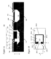
- FIG. 1A a cross-sectional view of a micromechanical device including an integrated accelerometer sensor and pressure sensor in a single crystal silicon chip 100 is illustrated.
- the left side of chip 100 includes the accelerometer 110 region of the integrated chip 100 and the right side of chip 100 includes the pressure sensor 120 region of the integrated chip 100.
- Accelerometer sensor 110 and pressure sensor 120 are formed over recesses 132 and 134 in a silicon wafer 130, for example, an N-type substrate.
- a silicon wafer 130 for example, an N-type substrate.
- an N-type silicon layer 144 Positioned over silicon wafer 130 is an N-type silicon layer 144.
- Layer 144 may include one or more actual epitaxial layers as will be described below.
- P-type piezoresistive sensor elements 150 are strategically implanted within layer 144 to sense flexure in the silicon structures.
- Chip 100 also includes an oxide/nitride layer 160 and metal interconnects 170 formed on the layer 144 to couple the piezoresistive sensor elements 150 to an exterior of the chip.
- Silicon wafer 130 may further be formed on a carrier wafer or substrate (not shown).
- P-type and N-type materials described herein can be used in an alternative fashion, e.g., by replacing P-type materials for N-type materials and vice versa.
- Figure 1 B illustrates a top view of the suspended structure of the accelerometer sensor of Figure 1A disposed above recess 132, however, for illustrative purposes metal interconnections 170, oxide layer 160, and piezoresistive elements 150 of Figure 1A are not shown.
- a beam 113 is suspended over recess 132.
- the beam 113 includes a flexure region 112 and a proof mass region 114.
- the beam 113 includes a generally horizontal boundary region 104-1 to 104-8, which surrounds the flexure region 112 and the proof mass region 114.
- a thinned flexure region 112 of the beam 113 is secured to thicker portions of the layer 144 along one boundary region portion 104-1 of the beam 113.
- the other boundary portions 104-2 to 104-8 of the beam 113 are released from layer 144 so that the beam 113 is suspended opposite the recess 132 and so that the beam 113 can flex most freely in a direction generally perpendicular to horizontal dimensions of layer 144.
- trenches are etched vertically completely through the layer 144 along boundary regions 104-2 to 104-8 so as to define a cantilever beam 113.
- Boundary region 104-1 which is not etched completely through, is thinned so as to produce a flexure region 112.
- the flexure region 112 comprises a proximal end of the beam 113 that is secured to an anchor region 115 of layer 144.
- the flexure region 112 is thin relative to an adjacent anchor region 115 of the layer 144 to which the flexure region 112 is secured.
- the anchor region 115 is suspended over the recess 132.
- the flexure region 112 also is thin relative to the proof mass region 114, which comprises a distal portion of the beam 113.
- the vertical dimension of the layer 144 is indicated by an arrow labeled z in the drawings.
- the vertical dimension is generally perpendicular to a horizontal plane of the layer 144.
- the thinness of the flexure 112 relative to the anchor region 115 to which it is secured facilitates flexure of the flexure region 112 resulting in generally rotational movement of the proof mass region 114 out of the plane of the layer 144 about a horizontal axis x-x that runs through the flexure region 112.
- the proof mass 114 may move, at least temporarily, to a position that is slightly above or slightly below a horizontal surface of the semiconductor layer 144.
- the horizontal dimensions of layer 144 are indicated by axes labeled x and y in the drawings. The horizontal dimensions are parallel to the horizontal plane of layer 144.
- the relative thickness of the proof mass region 114 further promotes such movement when, for example, an acceleration force is applied in a direction generally perpendicular to the horizontal dimension of the layer 144.
- Accelerometer sensor 110 thus operates by measuring the flexure in the beam 112 caused by motion of the proof mass 114 that is positioned over recess 132 and depends from layer 144 through beam 112.
- the flex or bend of beam 112 is sensed by one or more piezoresistive sensor elements 150 located near an anchor region 115, or base of beam 112, i.e., near the point where beam 112 depends from layer 144.
- the change in resistance of piezoresistive sensor elements 150 can be determined via metallization elements 170 to determine the amount of flexure and thus the acceleration experienced by the sensor.
- a cap 117 (shown in phantom lines) may be formed over the accelerometer portion of the chip 100 to protect the structures from environmental effects or contain a dampening fluid or gas around the proof mass 114.
- dimples 118 may be included on the bottom of recess 132 or the underside of cap 117 as over-range protection and anti-stiction structures, i.e., to prevent damage to the structure from large accelerations.
- Pressure sensor 120 operates by measuring flexure in the thinned structure or diaphragm 122 formed in layer 144 over the cavity between wafer layer 130 and layer 144.
- the diaphragm serves as a flexure structure in the pressure sensor. As the pressure outside of the cavity changes the diaphragm 122 will flex towards or away from cavity 134.
- pressure sensor 120 is formed with a vacuum within the cavity thereby forming an absolute-pressure sensor. Diaphragm 122 will flex inwards towards the cavity in a predictable way from pressure exerted on the diaphragm.
- the flexure in diaphragm 122 is detected by one or more piezoresistive sensor elements 150 formed in layer 144 on or near the edges of diaphragm 122.
- the resistance of piezoresistive elements 150 can be determined via a circuit, such as a wheatstone bridge circuit and the like, interconnected using metallization elements 170.
- the resistance of the piezoresistive elements 150 varies with flexure of the diaphragm 122. Thus, measurement of the piezoresistive resistance can be used to determine the amount of flexure and thus determine the pressure exerted on the sensor.
- circuitry and methods used to determine the amount of flexure of beam 112 or diaphragm 122 from the piezoresistive sense elements 150, and thus the amount of acceleration or pressure respectively employ techniques well-known to those skilled in the art and are not part of the present invention. For example, measuring changes in resistance, amplifying signals, and compensating for dependence on temperature with external circuits are well known. Hence, they need not be described in great details.
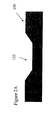
- Figure 2A illustrates a single crystal silicon substrate, or wafer 130 with N doping and a recessed region 132 formed therein.
- Recess region 132 is formed in the silicon wafer 130 using standard semiconductor techniques such as plasma etching, wet-etching with KOH or other silicon etchants, differential oxide growth, or the like.
- a high anisotropy etch can be employed, such as the "multiplex RIE system," that performs an inductively coupled plasma DRIE and is available from Surface Technology Systems (STS), which has a place of business in Palo Alto, California.
- a high anisotropy etch allows for a higher aspect ratio recessed region 132.
- Recessed region 132 can have any arbitrary geometry and can have any required depth, from less than 0.1 micron to greater than 100 microns, for example, depending on the particular application. Further, dimples 118 ( Figure 1A) can be formed in the bottom portion of recess 132 to avoid stiction when the proof mass 114 is displaced beyond its range.
- recessed region 132 need not have a single, uniform depth.
- the base of the recessed region can be either bare silicon, oxidized silicon, doped silicon, or it can be coated with any other thin film capable of withstanding subsequent wafer bonding and processing temperatures.
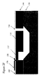
- Figure 2B illustrates a second silicon wafer 142, a P-type substrate silicon wafer with an N-type layer 144 formed thereon.
- a cavity or recess 146 is then etched from layer 144.
- Recess 146 can be etched by standard semiconductor techniques such as a silicon reactive ion etch (RIE), DRIE, KOH, wet etch, or the like. The etch is timed such that layer 144 is not fully etched through to the P-type substrate 142. Rather, a vertical thickness in layer 144 is left that corresponds to the desired thickness of beam 112 of the formed accelerometer sensor.
- RIE silicon reactive ion etch
- the first wafer 130 and second wafer 142 are appropriately aligned and secured together with the layer 144 therebetween.
- recess 146 of the layer 144 is aligned near and over one edge of recess 132 formed in the first wafer 130 and secured thereto by a silicon fusion bonding (or direct bonding) process.
- Fusion bonding techniques are well known. For example, refer to, K. E. Petersen, D. Gee, F. Pourahmadi, R. Craddock, J. Brown, and L. Christel, "Surface Micromachined Structures Fabricated with Silicon Fusion Bonding," Proceedings, Transducers 91, June 1991, at pp. 397-399 which is expressly incorporated herein by reference.
- the opposing surfaces are made hydrophilic. That is, they are treated with an agent such as hot nitric acid or a hot sulfuric acid and hydrogen peroxide solution or another strong oxidant that causes water to adhere to them.
- the two wafers then are placed in an oxidizing atmosphere at a temperature of 400 °C - 1200 °C for approximately one hour.
- the silicon fusion bonding technique described above bonds the first wafer 130 and the layer 144 together without the use of an intermediate glue material that could have a different coefficient of thermal expansion than the single crystal silicon wafer. Furthermore, fusion bonding can be performed in which oxide or nitride layers have been formed in the bonded surfaces of one or both of the wafers.
- the second wafer 142 is removed leaving layer 144 on wafer 130.
- the second wafer 142 is removed, for example, by an electrochemical KOH etch in which the layer 144 serves as an etch stop layer.
- one or more P-type piezoresistive sensor elements 150 are implanted near the base of beam 112 in layer 144.
- Boron implantation and diffusion at 1100 °C may form piezoresistive sensor elements 150.
- an insulating oxide/nitride layer 160 is formed over the layer 144 followed by the metallization of metal interconnects 170 coupled to the piezoresistive sensor elements 150.
- a deep reactive ion etch is performed to "release" beam 112 and proof mass 114, i.e., beam 112 and proof mass 114 are detached from layer 144, except the base of beam structure 112 such that proof mass 114 may move.
- the top surface of the layer 144 is first patterned with a relief pattern for the DRIE to form via 116 and release the accelerometer structure proof mass 114.
- An exemplary deep reactive ion etch is described, for example, in U.S. Patent No. 6,316,796, entitled, "SINGLE CRYSTAL SILICON SENSOR WITH HIGH ASPECT RATIO AND CURVILINEAR STRUCTURES".
- DRIE in essence, involves a synergistic action between chemical etch and ion bombardment. Impinging energized ions chemically react with the silicon surface.
- the DRIE process advantageously etches in the vertical direction at a much higher rate than in the lateral direction, e.g., anisotropically, regardless of silicon crystal planes or crystal orientation.
- relatively deep substantially vertical trenches or slots can be formed in layer 144. These substantially vertical trenches or slots can be formed anywhere in layer 144 regardless of crystallographic orientation within the silicon material. Consequently, high aspect ratio vias can be formed to release beam 112 and proof mass 114 while allowing for a small overall chip size.
- the DRIE etching step defines and mechanically "releases" proof mass 114 from layer 144 thereby allowing beam 112 and proof mass 114 to move relative to wafer 130 and layer 144.
- proof mass 114 may move up or down out of the plane of the layer 144 in response to an acceleration of the accelerometer sensor.
- the movement of proof mass 114 causes flexure in the beam 112 that is sensed by one or more piezoresistive sensor elements 150.
- the accelerometer sensor can be encapsulated using a cap 117, for example, to isolate the structures from environmental effects such as humidity, or to isolate the beam 112 and proof mass 114 within a vacuum or dampening fluid or gas.
- dimples 118 ( Figure 1A) may be included on the bottom of the recess or the underside of a cap to prevent stiction when an over range displacement occurs.
- Thickness, and therefore massiveness of the proof mass portion of beam 112 can be determined by the thickness of layer 144.
- Thinness of the flexure portion of beam 112 can be determined by the etch process described with reference to Figure 2B.
- the second silicon wafer 142 serves as a convenient carrier (or handle) for the layer 144 that is being etched.
- a smaller suspended beam structure can be produced in which flexure region thinness and seismic mass thickness are selected to achieve desired sensitivity to changes in acceleration.
- FIG. 3A - 3E an exemplary method of manufacturing a pressure sensor such as the one illustrated in Figure 1A is illustrated. It will be understood that many details of the processes described with reference to Figures 2A - 2F are used during the fabrication steps described with respect to Figures 3A - 3E. Accordingly, these process details will not be reiterated with reference to Figures 3A - 3E. Further, the method in Figures 3A - 3E is similar in certain aspects to the method illustrated in Figures 2A - 2F for forming the accelerometer sensor and can be advantageously integrated into a single chip in parallel or in series. The integrated sensors in a single chip can be used, for example, in a remote tire pressure and acceleration monitoring system or the like.
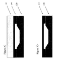
- Figure 3A illustrates a first wafer 130, an N type substrate, with a recessed region 134 formed therein.
- the recessed area 134 is formed by standard semiconductor manufacturing processes, such as a KOH etch or the like. Recessed area can be any arbitrary geometry and will serve as part of the inner cavity of the formed pressure sensor.
- Figure 3B illustrates a second silicon wafer 142, a P-type substrate wafer, with an N-type layer 144 formed thereon.
- a recessed region 148 is etched from layer 144 via a RIE, DRIE, wet etch, or the like.
- Layer 144 is patterned and a timed etch is performed to etch partially into layer 144 leaving a desired thickness of layer 144.
- the recessed portion of layer 144 will correspond to a thin diaphragm 122 of the formed pressure sensor.
- first wafer 130 and second wafer 142 are appropriately aligned with recess 134 facing recess 148.
- the first wafer 130 and second wafer 142 are secured to each other.
- recess 148 of layer 144 is aligned over the cavity 134 formed in first wafer 130.
- first wafer 130 and second wafer 142 are secured through silicon fusion bonding.
- P-type substrate of second wafer 142 is then removed, for example, by an electrochemical KOH etch or the like leaving layer 144 on the first wafer 130 as seen in Figure 3D.
- one or more P-type piezoresistive sensor elements 150 are implanted near the edges of thin diaphragm 122 formed as part of layer 144. Piezoresistive sensor elements 150 are positioned to sense flexure in diaphragm 122. It should be noted that any number of piezoresistive sensor elements 150 may be employed and their exact positioning relative to the diaphragm 122 may be different depending on the particular application, expected pressures, sensitivity requirements, and the like. Further, an oxide/nitride layer 160 is deposited over layer 144 followed by the metallization of the metal interconnects 170.
- the methods illustrated in Figures 2A through 2F and Figures 3A through 3E can be performed in parallel or in series to form integrated accelerometer sensors and pressure sensors on a single chip. Performing the process in parallel offers the advantages of greater processing throughput, i.e., fewer total processing steps for the combined chip. Also, the parallel process allows for beam 112 thickness to be independent of the thickness of diaphragm 122. For instance, by etching the recess 146 and 148 in layer 144 to different depths for beam 112 and diaphragm 122 the thickness and sensitivity of each sensor can be individually optimized.
- Figures 4A - 4H illustrate another exemplary method for fabricating an accelerometer sensor and pressure sensor in parallel on a single silicon crystal chip.
- beam 112', proof mass 114', and diaphragm 122' are built up with multiple semiconductor layers, or sublayers to form desired structures.
- a first N-type substrate, wafer 130' is patterned and etched to form recessed area 132' and recessed area 134', corresponding to recessed areas for the accelerometer sensor and the pressure sensor respectively.
- a second P-type substrate, wafer 142' with an N-type layer 144' is placed over and silicon fusion bonded to the first silicon wafer 130'.
- the layer 144' is not thinned, i.e., etched, prior to the silicon fusion bonding.
- the second wafer 142' is electrochemically etched back using KOH or the like to layer 144' in Figure 4C.
- Layer 144' is left bonded to the first wafer 130' and covers recess 132' and recess 134'.
- the top or exposed surface of the layer 144' is then patterned and etched with a DRIE.
- Layer 144' is patterned such that the DRIE forms an opening in layer 144' and above recessed region 132'. This opening will correspond to the thinned region of beam 112'.
- a second semiconductor layer 145' will be placed over layer 144' and will serve, in part, as beam 112'.
- Layer 144' is further patterned such that the DRIE forms an opening in layer 144' above recessed region 134'. This opening corresponds to the sidewalls of the cavity of the pressure sensor with second layer 145' layered over layer 144' to form the diaphragm 122'.
- a third P-type substrate, wafer 143' with an N-type epitaxial layer 145' is placed over layer 144' and silicon fusion bonded together as described above.
- the silicon wafer 143' is electrochemically etched away with a KOH etch or the like with the epitaxial layer 145' serving as an etch stop.
- Epitaxial layer 145' is, for example, the same material as epitaxial layer 144'.
- epitaxial layer 144' and 145' may include different materials
- multiple P-type piezoresistive sensor elements 150' are then implanted in second layer 145'.
- One piezoresistive sensor element 150' is implanted near the base of the thin region or beam 112', i.e., the region of layer 145' above the via etched in layer 144', to sense flexure in beam 112'.
- Additional piezoresistive sensor elements 150' are implanted in the second layer 145' near the edges of the thin diaphragm of the pressure sensor to sense flexure in the diaphragm.
- an oxide/nitride layer 170' is deposited over the layer 145' followed by the metallization of metal interconnects 170'.
- a second DRIE is performed to release the accelerometer structure, i.e., the proof mass 114' from the layer 144' and 145'.
- the top surface of the second layer 145' is patterned and a DRIE performed to etch a relief pattern or via 116' to release beam 112' and proof mass 114'.
- Proof mass 114' consists of both the first and second layers 144' and 145' and is attached to the remainder of the chip structure through beam structure 112' which includes a portion of second layer 145'.
- the accelerometer can be encapsulated with a cap (not shown) to protect the structures of the accelerometer sensor or to contain a vacuum, fluid, or gas around proof mass 114'.
- the cavity formed within the pressure sensor can be manufactured at a vacuum to measure absolute pressures.
- the accelerometer and pressure sensor can be manufactured on a single chip in series or in parallel with any of the exemplary methods described.
Abstract
Description
- The invention relates generally to semiconductor microelectromechanical devices or micromechanical force sensors that can be used to detect small forces or flexures generated from chemo-mechanical stress, thermal stress, electromagnetic fields, and the like. More particularly, but not limited to, the invention relates to integrated piezoresistive accelerometers and pressure sensors that may be manufactured on a single chip.
- Advances in semiconductor microelectronic sensors have served to greatly reduce the size and cost of such sensors. The electrical and mechanical properties of silicon microsensors have been well chronicled. For example, refer to Kurt E. Petersen, "Silicon as a Mechanical Material," Proceedings of the IEEE, vol. 70, No. 5, May 1982. Moreover, there is a large and growing body of knowledge concerning techniques for constructing silicon microstructures, commonly referred to as "micromachining." See, for example, Bryzek, Petersen and McCulley, "Micromachines on the March," IEEE Spectrum, May 1994, pp. 20 - 31.
- Thus, silicon micromachining and semiconductor microelectronic sensors have blossomed into a vital industry with numerous practical applications. For instance, micromachined silicon pressure sensors, acceleration sensors, flow sensor, and the like have found their way into various applications and industries ranging from medical instruments to automobiles. The high strength, elasticity, and resilience of silicon makes it an ideal base material for resonant structures that may, for example, be useful for electronic frequency control or sensor structures. Even consumer items such as watches, scuba diving equipment, hand-held tire pressure gages, and inflatable tennis shoes may soon incorporate silicon micromachined sensors.
- The demand for silicon sensors in ever expanding fields of use continues to fuel a need for new and different silicon microsensor geometries and configurations optimized for particular environments and applications. Unfortunately, a drawback of traditional bulk silicon micromachining techniques has been that the contours and geometries of the resulting silicon microstructures have been significantly limited by these fabrication methods. For instance, etching silicon structures with conventional etching techniques is constrained, in part, by the crystal orientations of silicon substrates, which limits the geometry and miniaturization efforts of many desired structures.
- The increasing use of microsensors to measure pressure or acceleration has spurred the development of small silicon plate structures used, for example, as capacitors and to produce electrostatic forces. For instance, there exist microsensors that measure capacitance using an array of interdigitated polysilicon plates. Similarly, there exist microsensors that produce electrostatic forces using an array of interdigitated plates. Further, there exist microsensors that measure the flexure, or bending, of silicon structures in response to forces such as weight or acceleration.
- In many applications it is desired to obtain both pressure and acceleration measurements. In such applications, fabricating both pressure and accelerometer sensors on a single chip would be advantageous. As pressure and accelerometer sensors are fabricated to smaller dimensions, it is desired to integrate both types of sensors on a single chip and at the same time optimize the material and structural characteristics as well as the methods of manufacturing. It is further desired to manufacture small accelerometer sensors with high sensitivity. Consequently, there has been a need for a single chip integrated accelerometer sensors and pressure sensors, and a method of fabricating accelerometer sensors and pressure sensors on a single chip.
- The expanding fields of use of micromechanical devices in general, and of accelerometers and pressure sensors in particular, has created a demand for even smaller devices. Unfortunately, there has been difficulty producing smaller devices that are also highly sensitive to small changes in acceleration or pressure. For example, there has been a need for a smaller accelerometer that combines sufficiently thin flexure structures with a sufficiently large proof mass (or seismic mass) to be responsive to small changes in acceleration.
- The present invention meets these needs.
- In one aspect of the invention, a micromechanical device comprises a first semiconductor wafer that defines a recessed region. A semiconductor layer is secured to the wafer opposite the recessed region. A cantilever beam is formed in the semiconductor layer. The cantilever beam includes a flexure region secured to an anchor region of the semiconductor layer and includes a proof mass region suspended opposite the first recessed region. The flexure region is thin relative to the anchor region of the semiconductor layer.
- In one embodiment, a vertical dimension of the flexure region is thin relative to a vertical dimension of the anchor region of the semiconductor layer so as to promote rotational movement of the proof mass out of the horizontal plane of the semiconductor layer about an axis through the flexure region in response to an acceleration force applied in a direction generally perpendicular to the horizontal plane of the semiconductor layer.
- In another aspect of the invention, a method of sensing acceleration uses a cantilever beam suspended over a recessed region of a semiconductor wafer. An acceleration force is applied in a direction generally perpendicular to a horizontal plane of the semiconductor wafer. Flexure of the beam in a direction generally parallel to the direction of the acceleration force sensed.
- In yet another aspect, a micromechanical device and method of producing the device are provided. In one embodiment, the device includes an accelerometer with a thinned cantilever structure. In another embodiment, the device includes an accelerometer and a pressure sensor integrated on a single chip.
- The present invention is better understood upon consideration of the detailed description below in conjunction with the accompanying drawings, in which:
- Figure 1A is a cross-sectional view of an exemplary integrated accelerometer and pressure sensor on a single silicon chip;
- Figure 1 B is a top view of an exemplary accelerometer sensor;
- Figures 2A through 2F are cross-sectional views of an exemplary process for manufacturing accelerometer sensors using Silicon Fusion Bonding (SFB) and a Deep Reactive Ion Etch (DRIE);
- Figures 3A through 3E are cross-sectional views of an exemplary process for manufacturing absolute pressure sensors using Silicon Fusion Bonding (SFB) and a Deep Reactive Ion Etch (DRIE); and
- Figures 4A through 4H are cross-sectional views of an alternative exemplary process for manufacturing both accelerometer sensors and pressure sensors using Silicon Fusion Bonding (SFB) and a Deep Reactive Ion Etch (DRIE).
-
- The present invention provides a semiconductor micromechanical device with a thinned cantilever structure and associated methods of manufacture. The following description is presented to enable any person skilled in the art to make and use the invention. Descriptions of specific applications are provided only as examples. Various modifications to the preferred embodiment will be readily apparent to those skilled in the art, and the general principles defined herein may be applied to other embodiments and applications without departing from the spirit and scope of the invention. Thus, the present invention is not intended to be limited to the embodiments shown, but is to be accorded the widest scope consistent with the principles and features disclosed herein.
- One exemplary device and manufacturing process in accordance with an embodiment of the invention provides an integrated piezoresistor accelerometer and pressure sensor using silicon fusion bonding and deep reactive ion etch. The exemplary device and process integrates piezoresistor accelerometers with a proof mass (sometimes referred to as a seismic mass) and absolute pressure sensors on a single chip.
- Another exemplary device and manufacturing process in accordance with another embodiment of the invention provides an accelerometer manufactured with a thinned cantilever beam including a flexure region and relatively large proof mass. The exemplary accelerometer with a thinned beam offers improved sensitivity through use of a flexure with smaller structural dimensions.
- The exemplary devices and manufacturing processes offer several advantages over existing processes. For instance, the overall chip size may be made smaller than conventional chips because the process does not require a potassium hydroxide (KOH) etch from the backside of the wafer, i.e., "backside etching." Further, the planar manufacturing processes are ideal for manufacturing purposes. Thinning the flexure beam in relation to the proof mass allow for increased sensitivity with small structure dimensions. Further, in an integrated accelerometer and pressure sensor chip process the beam flexure thickness can be sized independent of the diaphragm thickness while maintaining a planar top surface and efficient manufacturing processes.
- The devices and manufacturing processes also allow for over-range protection and anti-stiction mechanisms to be easily included in the accelerometer portion of the structure. Additionally, only a single cap is needed for the chip, e.g., to cover the proof mass of the accelerometer, as compared to conventional chips that typically require a second cap for the pressure sensor. The exemplary single chip processes therefore allow for greater design flexibility and a smaller chip size with simplified manufacturing processes.
- An integrated chip with an accelerometer and pressure sensor may be used in many applications. One exemplary application is remote tire pressure monitoring. A small chip with integrated accelerometers and pressure sensors is ideal for remotely indicating tire pressure in relation to a vehicle's speed or acceleration (linear speed and acceleration can be derived from the rotational acceleration experienced by the accelerometer). The single integrated chip can be packaged or coupled with an ASIC chip or the like to remotely retrieve and manipulate the piezoresistive sensor readings related to pressure and acceleration.
- It should be recognized, however, that the integrated chip and associated methods of manufacture are useful in a wide variety of other applications not explicitly described herein to monitor acceleration or pressure.
- An exemplary micromachined accelerometer sensor is made by forming a proof mass that extends away from a larger body of a silicon wafer and is attached thereto by a cantilever beam. In this embodiment, the beam acts as a flexure structure. Accelerometer sensors measure acceleration by sensing the movement of the proof mass relative to the wafer or substrate. In particular, as the proof mass moves relative to the wafer, properly placed piezoresistive sensor elements near or on the beam sense flexure in the beam caused by the movement of the proof mass indicated by a change in resistance of the piezoresistive sensor element.
- Accelerometer sensitivity is achieved by thinning a flexure region of a cantilever beam in relation to the distally located larger proof mass. Accelerometers sensors may thus be made to smaller dimensions without unnecessary loss of sensitivity to small changes in acceleration. The flexure beam can be made thinner, for example, by forming a recess in a semiconductor layer prior to bonding to the substrate. Alternatively, multiple semiconductor layers can be layered over the substrate and etched to form recesses therein.
- An exemplary micromachined absolute-pressure sensor can be made by forming a cavity within a silicon structure and a diaphragm adjacent to the cavity. For an absolute-pressure sensor the cavity is held in a vacuum. The absolute-pressure sensor measures pressure by sensing the flexure of the diaphragm, e.g., how the pressure acting on the front side of the diaphragm deflects the diaphragm inwards. One or more piezoresistive sensors formed near the edges of the diaphragm typically sense the flexure or deflection of the diaphragm.
- Referring to Figure 1A, a cross-sectional view of a micromechanical device including an integrated accelerometer sensor and pressure sensor in a single
crystal silicon chip 100 is illustrated. The left side ofchip 100 includes theaccelerometer 110 region of theintegrated chip 100 and the right side ofchip 100 includes thepressure sensor 120 region of theintegrated chip 100.Accelerometer sensor 110 andpressure sensor 120 are formed overrecesses silicon wafer 130, for example, an N-type substrate. Positioned oversilicon wafer 130 is an N-type silicon layer 144.Layer 144 may include one or more actual epitaxial layers as will be described below. P-typepiezoresistive sensor elements 150 are strategically implanted withinlayer 144 to sense flexure in the silicon structures.Chip 100 also includes an oxide/nitride layer 160 andmetal interconnects 170 formed on thelayer 144 to couple thepiezoresistive sensor elements 150 to an exterior of the chip.Silicon wafer 130 may further be formed on a carrier wafer or substrate (not shown). - It should be recognized that the P-type and N-type materials described herein can be used in an alternative fashion, e.g., by replacing P-type materials for N-type materials and vice versa.
- With reference to Figure 1A and 1B, an exemplary accelerometer sensor and operation thereof is described. Figure 1 B illustrates a top view of the suspended structure of the accelerometer sensor of Figure 1A disposed above
recess 132, however, for illustrativepurposes metal interconnections 170,oxide layer 160, andpiezoresistive elements 150 of Figure 1A are not shown. Abeam 113 is suspended overrecess 132. Thebeam 113 includes aflexure region 112 and a proofmass region 114. Thebeam 113 includes a generally horizontal boundary region 104-1 to 104-8, which surrounds theflexure region 112 and the proofmass region 114. A thinnedflexure region 112 of thebeam 113 is secured to thicker portions of thelayer 144 along one boundary region portion 104-1 of thebeam 113. The other boundary portions 104-2 to 104-8 of thebeam 113 are released fromlayer 144 so that thebeam 113 is suspended opposite therecess 132 and so that thebeam 113 can flex most freely in a direction generally perpendicular to horizontal dimensions oflayer 144. - More specifically, trenches are etched vertically completely through the
layer 144 along boundary regions 104-2 to 104-8 so as to define acantilever beam 113. Boundary region 104-1, which is not etched completely through, is thinned so as to produce aflexure region 112. Theflexure region 112 comprises a proximal end of thebeam 113 that is secured to ananchor region 115 oflayer 144. Theflexure region 112 is thin relative to anadjacent anchor region 115 of thelayer 144 to which theflexure region 112 is secured. In the embodiment of Figures 1A - 1 B, theanchor region 115 is suspended over therecess 132. It will be appreciated, however, that theanchor region 115 need not be suspended, as best shown in the alternative embodiment described with reference to Figure 2F. Theflexure region 112 also is thin relative to the proofmass region 114, which comprises a distal portion of thebeam 113. The thinness of theflexure region 112 relative to theanchor region 115 to which it is secured, promotes movement of thecantilever beam 113 in a direction generally parallel to a vertical dimension of thelayer 144. The vertical dimension of thelayer 144 is indicated by an arrow labeled z in the drawings. The vertical dimension is generally perpendicular to a horizontal plane of thelayer 144. - In particular, the thinness of the
flexure 112 relative to theanchor region 115 to which it is secured facilitates flexure of theflexure region 112 resulting in generally rotational movement of the proofmass region 114 out of the plane of thelayer 144 about a horizontal axis x-x that runs through theflexure region 112. For example, as theflexure region 112 flexes in response to an acceleration force, theproof mass 114 may move, at least temporarily, to a position that is slightly above or slightly below a horizontal surface of thesemiconductor layer 144. The horizontal dimensions oflayer 144 are indicated by axes labeled x and y in the drawings. The horizontal dimensions are parallel to the horizontal plane oflayer 144. The relative thickness of the proofmass region 114 further promotes such movement when, for example, an acceleration force is applied in a direction generally perpendicular to the horizontal dimension of thelayer 144. -
Accelerometer sensor 110 thus operates by measuring the flexure in thebeam 112 caused by motion of theproof mass 114 that is positioned overrecess 132 and depends fromlayer 144 throughbeam 112. The flex or bend ofbeam 112 is sensed by one or morepiezoresistive sensor elements 150 located near ananchor region 115, or base ofbeam 112, i.e., near the point wherebeam 112 depends fromlayer 144. The change in resistance ofpiezoresistive sensor elements 150 can be determined viametallization elements 170 to determine the amount of flexure and thus the acceleration experienced by the sensor. - Further, a cap 117 (shown in phantom lines) may be formed over the accelerometer portion of the
chip 100 to protect the structures from environmental effects or contain a dampening fluid or gas around theproof mass 114. Additionally, dimples 118 may be included on the bottom ofrecess 132 or the underside ofcap 117 as over-range protection and anti-stiction structures, i.e., to prevent damage to the structure from large accelerations. For example, thecap 117 anddimples 118 may protect the silicon structure for shock forces up to 10,000 G (1 G = 9.81 m/s2). -
Pressure sensor 120 operates by measuring flexure in the thinned structure ordiaphragm 122 formed inlayer 144 over the cavity betweenwafer layer 130 andlayer 144. The diaphragm serves as a flexure structure in the pressure sensor. As the pressure outside of the cavity changes thediaphragm 122 will flex towards or away fromcavity 134. In one example,pressure sensor 120 is formed with a vacuum within the cavity thereby forming an absolute-pressure sensor.Diaphragm 122 will flex inwards towards the cavity in a predictable way from pressure exerted on the diaphragm. The flexure indiaphragm 122 is detected by one or morepiezoresistive sensor elements 150 formed inlayer 144 on or near the edges ofdiaphragm 122. The resistance ofpiezoresistive elements 150 can be determined via a circuit, such as a wheatstone bridge circuit and the like, interconnected usingmetallization elements 170. The resistance of thepiezoresistive elements 150 varies with flexure of thediaphragm 122. Thus, measurement of the piezoresistive resistance can be used to determine the amount of flexure and thus determine the pressure exerted on the sensor. - Details of the circuitry and methods used to determine the amount of flexure of
beam 112 ordiaphragm 122 from thepiezoresistive sense elements 150, and thus the amount of acceleration or pressure respectively, employ techniques well-known to those skilled in the art and are not part of the present invention. For example, measuring changes in resistance, amplifying signals, and compensating for dependence on temperature with external circuits are well known. Hence, they need not be described in great details. - An exemplary process for fabricating a silicon accelerometer sensor like the one illustrated in Figure 1A is explained with reference to the illustrations depicted in Figures 2A - 2F. Figure 2A illustrates a single crystal silicon substrate, or
wafer 130 with N doping and a recessedregion 132 formed therein.Recess region 132 is formed in thesilicon wafer 130 using standard semiconductor techniques such as plasma etching, wet-etching with KOH or other silicon etchants, differential oxide growth, or the like. Additionally, a high anisotropy etch can be employed, such as the "multiplex RIE system," that performs an inductively coupled plasma DRIE and is available from Surface Technology Systems (STS), which has a place of business in Palo Alto, California. A high anisotropy etch allows for a higher aspect ratio recessedregion 132. - Recessed
region 132 can have any arbitrary geometry and can have any required depth, from less than 0.1 micron to greater than 100 microns, for example, depending on the particular application. Further, dimples 118 (Figure 1A) can be formed in the bottom portion ofrecess 132 to avoid stiction when theproof mass 114 is displaced beyond its range. - It should be further noted that recessed
region 132 need not have a single, uniform depth. Further, the base of the recessed region can be either bare silicon, oxidized silicon, doped silicon, or it can be coated with any other thin film capable of withstanding subsequent wafer bonding and processing temperatures. - Figure 2B illustrates a
second silicon wafer 142, a P-type substrate silicon wafer with an N-type layer 144 formed thereon. A cavity orrecess 146 is then etched fromlayer 144. Recess 146 can be etched by standard semiconductor techniques such as a silicon reactive ion etch (RIE), DRIE, KOH, wet etch, or the like. The etch is timed such thatlayer 144 is not fully etched through to the P-type substrate 142. Rather, a vertical thickness inlayer 144 is left that corresponds to the desired thickness ofbeam 112 of the formed accelerometer sensor. - With reference to Figure 2C, the
first wafer 130 andsecond wafer 142 are appropriately aligned and secured together with thelayer 144 therebetween. In a present embodiment,recess 146 of thelayer 144 is aligned near and over one edge ofrecess 132 formed in thefirst wafer 130 and secured thereto by a silicon fusion bonding (or direct bonding) process. Fusion bonding techniques are well known. For example, refer to, K. E. Petersen, D. Gee, F. Pourahmadi, R. Craddock, J. Brown, and L. Christel, "Surface Micromachined Structures Fabricated with Silicon Fusion Bonding," Proceedings, Transducers 91, June 1991, at pp. 397-399 which is expressly incorporated herein by reference. In one exemplary fusion bonding technique, the opposing surfaces are made hydrophilic. That is, they are treated with an agent such as hot nitric acid or a hot sulfuric acid and hydrogen peroxide solution or another strong oxidant that causes water to adhere to them. The two wafers then are placed in an oxidizing atmosphere at a temperature of 400 °C - 1200 °C for approximately one hour. - The silicon fusion bonding technique described above bonds the
first wafer 130 and thelayer 144 together without the use of an intermediate glue material that could have a different coefficient of thermal expansion than the single crystal silicon wafer. Furthermore, fusion bonding can be performed in which oxide or nitride layers have been formed in the bonded surfaces of one or both of the wafers. - With reference now to Figure 2D, after the opposing surfaces of the
wafer 130 andlayer 144 have been bonded, thesecond wafer 142 is removed leavinglayer 144 onwafer 130. Thesecond wafer 142 is removed, for example, by an electrochemical KOH etch in which thelayer 144 serves as an etch stop layer. - With reference to Figure 2E, one or more P-type
piezoresistive sensor elements 150 are implanted near the base ofbeam 112 inlayer 144. For example, Boron implantation and diffusion at 1100 °C may formpiezoresistive sensor elements 150. Further, an insulating oxide/nitride layer 160 is formed over thelayer 144 followed by the metallization ofmetal interconnects 170 coupled to thepiezoresistive sensor elements 150. - With reference to Figure 2F, a deep reactive ion etch (DRIE) is performed to "release"
beam 112 andproof mass 114, i.e.,beam 112 andproof mass 114 are detached fromlayer 144, except the base ofbeam structure 112 such thatproof mass 114 may move. The top surface of thelayer 144 is first patterned with a relief pattern for the DRIE to form via 116 and release the accelerometer structureproof mass 114. An exemplary deep reactive ion etch is described, for example, in U.S. Patent No. 6,316,796, entitled, "SINGLE CRYSTAL SILICON SENSOR WITH HIGH ASPECT RATIO AND CURVILINEAR STRUCTURES". - DRIE, in essence, involves a synergistic action between chemical etch and ion bombardment. Impinging energized ions chemically react with the silicon surface. The DRIE process advantageously etches in the vertical direction at a much higher rate than in the lateral direction, e.g., anisotropically, regardless of silicon crystal planes or crystal orientation. As a result, relatively deep substantially vertical trenches or slots can be formed in
layer 144. These substantially vertical trenches or slots can be formed anywhere inlayer 144 regardless of crystallographic orientation within the silicon material. Consequently, high aspect ratio vias can be formed to releasebeam 112 andproof mass 114 while allowing for a small overall chip size. - The DRIE etching step defines and mechanically "releases"
proof mass 114 fromlayer 144 thereby allowingbeam 112 andproof mass 114 to move relative towafer 130 andlayer 144. For example,proof mass 114 may move up or down out of the plane of thelayer 144 in response to an acceleration of the accelerometer sensor. The movement ofproof mass 114 causes flexure in thebeam 112 that is sensed by one or morepiezoresistive sensor elements 150. - Additionally, the accelerometer sensor can be encapsulated using a
cap 117, for example, to isolate the structures from environmental effects such as humidity, or to isolate thebeam 112 andproof mass 114 within a vacuum or dampening fluid or gas. Additionally, dimples 118 (Figure 1A) may be included on the bottom of the recess or the underside of a cap to prevent stiction when an over range displacement occurs. - Thus, a small highly sensitive accelerometer can be produced. Thickness, and therefore massiveness of the proof mass portion of
beam 112 can be determined by the thickness oflayer 144. Thinness of the flexure portion ofbeam 112 can be determined by the etch process described with reference to Figure 2B. Moreover, during the etch process of Figure 2B, thesecond silicon wafer 142 serves as a convenient carrier (or handle) for thelayer 144 that is being etched. Thus, a smaller suspended beam structure can be produced in which flexure region thinness and seismic mass thickness are selected to achieve desired sensitivity to changes in acceleration. - With reference to Figures 3A - 3E, an exemplary method of manufacturing a pressure sensor such as the one illustrated in Figure 1A is illustrated. It will be understood that many details of the processes described with reference to Figures 2A - 2F are used during the fabrication steps described with respect to Figures 3A - 3E. Accordingly, these process details will not be reiterated with reference to Figures 3A - 3E. Further, the method in Figures 3A - 3E is similar in certain aspects to the method illustrated in Figures 2A - 2F for forming the accelerometer sensor and can be advantageously integrated into a single chip in parallel or in series. The integrated sensors in a single chip can be used, for example, in a remote tire pressure and acceleration monitoring system or the like.
- Figure 3A illustrates a
first wafer 130, an N type substrate, with a recessedregion 134 formed therein. The recessedarea 134 is formed by standard semiconductor manufacturing processes, such as a KOH etch or the like. Recessed area can be any arbitrary geometry and will serve as part of the inner cavity of the formed pressure sensor. - Figure 3B illustrates a
second silicon wafer 142, a P-type substrate wafer, with an N-type layer 144 formed thereon. A recessedregion 148 is etched fromlayer 144 via a RIE, DRIE, wet etch, or the like.Layer 144 is patterned and a timed etch is performed to etch partially intolayer 144 leaving a desired thickness oflayer 144. The recessed portion oflayer 144 will correspond to athin diaphragm 122 of the formed pressure sensor. - With reference to Figure 3C, the
first wafer 130 andsecond wafer 142 are appropriately aligned withrecess 134 facingrecess 148. Thefirst wafer 130 andsecond wafer 142 are secured to each other. In particular,recess 148 oflayer 144 is aligned over thecavity 134 formed infirst wafer 130. In a present embodiment,first wafer 130 andsecond wafer 142 are secured through silicon fusion bonding. P-type substrate ofsecond wafer 142 is then removed, for example, by an electrochemical KOH etch or the like leavinglayer 144 on thefirst wafer 130 as seen in Figure 3D. - With reference to Figure 3E, one or more P-type
piezoresistive sensor elements 150 are implanted near the edges ofthin diaphragm 122 formed as part oflayer 144.Piezoresistive sensor elements 150 are positioned to sense flexure indiaphragm 122. It should be noted that any number ofpiezoresistive sensor elements 150 may be employed and their exact positioning relative to thediaphragm 122 may be different depending on the particular application, expected pressures, sensitivity requirements, and the like. Further, an oxide/nitride layer 160 is deposited overlayer 144 followed by the metallization of the metal interconnects 170. - The methods illustrated in Figures 2A through 2F and Figures 3A through 3E can be performed in parallel or in series to form integrated accelerometer sensors and pressure sensors on a single chip. Performing the process in parallel offers the advantages of greater processing throughput, i.e., fewer total processing steps for the combined chip. Also, the parallel process allows for
beam 112 thickness to be independent of the thickness ofdiaphragm 122. For instance, by etching therecess layer 144 to different depths forbeam 112 anddiaphragm 122 the thickness and sensitivity of each sensor can be individually optimized. - Figures 4A - 4H illustrate another exemplary method for fabricating an accelerometer sensor and pressure sensor in parallel on a single silicon crystal chip. In this exemplary method, beam 112', proof mass 114', and diaphragm 122' are built up with multiple semiconductor layers, or sublayers to form desired structures. Again, it will be understood that many details for the processes described with reference to Figures 2A - 2F are used during the fabrication steps described with respect to Figures 4A - 4H. Accordingly, these process details will not be reiterated with reference to Figures 4A - 4H.
- With reference to Figure 4A, a first N-type substrate, wafer 130' is patterned and etched to form recessed area 132' and recessed area 134', corresponding to recessed areas for the accelerometer sensor and the pressure sensor respectively.
- With reference to Figure 4B, a second P-type substrate, wafer 142' with an N-type layer 144' is placed over and silicon fusion bonded to the first silicon wafer 130'. In this exemplary process, which differs from the process described above, the layer 144' is not thinned, i.e., etched, prior to the silicon fusion bonding. The second wafer 142' is electrochemically etched back using KOH or the like to layer 144' in Figure 4C. Layer 144' is left bonded to the first wafer 130' and covers recess 132' and recess 134'.
- With reference to Figure 4D, the top or exposed surface of the layer 144' is then patterned and etched with a DRIE. Layer 144' is patterned such that the DRIE forms an opening in layer 144' and above recessed region 132'. This opening will correspond to the thinned region of beam 112'. As will be described below with reference to Figure 4E, a second semiconductor layer 145' will be placed over layer 144' and will serve, in part, as beam 112'.
- Layer 144' is further patterned such that the DRIE forms an opening in layer 144' above recessed region 134'. This opening corresponds to the sidewalls of the cavity of the pressure sensor with second layer 145' layered over layer 144' to form the diaphragm 122'.
- With reference to Figure 4F, a third P-type substrate, wafer 143' with an N-type epitaxial layer 145' is placed over layer 144' and silicon fusion bonded together as described above. Similarly, the silicon wafer 143' is electrochemically etched away with a KOH etch or the like with the epitaxial layer 145' serving as an etch stop. Epitaxial layer 145' is, for example, the same material as epitaxial layer 144'. Alternatively, epitaxial layer 144' and 145' may include different materials
- With reference to Figure 4G, multiple P-type piezoresistive sensor elements 150' are then implanted in second layer 145'. One piezoresistive sensor element 150' is implanted near the base of the thin region or beam 112', i.e., the region of layer 145' above the via etched in layer 144', to sense flexure in beam 112'. Additional piezoresistive sensor elements 150' are implanted in the second layer 145' near the edges of the thin diaphragm of the pressure sensor to sense flexure in the diaphragm. Further an oxide/nitride layer 170' is deposited over the layer 145' followed by the metallization of metal interconnects 170'.
- Additionally, with reference to Figure 4H, a second DRIE is performed to release the accelerometer structure, i.e., the proof mass 114' from the layer 144' and 145'. The top surface of the second layer 145' is patterned and a DRIE performed to etch a relief pattern or via 116' to release beam 112' and proof mass 114'. Proof mass 114' consists of both the first and second layers 144' and 145' and is attached to the remainder of the chip structure through beam structure 112' which includes a portion of second layer 145'.
- Additionally, as described above, the accelerometer can be encapsulated with a cap (not shown) to protect the structures of the accelerometer sensor or to contain a vacuum, fluid, or gas around proof mass 114'. Also, the cavity formed within the pressure sensor can be manufactured at a vacuum to measure absolute pressures.
- The above detailed description is provided to illustrate exemplary embodiments and is not intended to be limiting. For example, the accelerometer and pressure sensor can be manufactured on a single chip in series or in parallel with any of the exemplary methods described.
- For completeness, various aspects of the invention are set out in the following numbered clauses:
- 1. A micromechanical device comprising:
- a first semiconductor wafer (130) defining a first recessed region (132) formed therein;
- a semiconductor layer (144) secured to the first wafer (130) opposite the first recessed region (132), the semiconductor layer (144) including a generally planar horizontal dimension;
- a cantilever beam (113) formed in the semiconductor layer (144); wherein the cantilever beam (113) includes a flexure region (112) that is secured to an anchor region (115) of the semiconductor layer (144);
- 2. The device of clause 1,
wherein the flexure region (112) is thin relative to the proof mass region (114). - 3. The device of clause 1 wherein a vertical dimension of the flexure region (112) is thin relative to a vertical dimension of the anchor region (115) of the semiconductor layer (144) so as to promote rotational movement of the proof mass (114) out of the horizontal plane of the semiconductor layer (144) about an axis (x) through the flexure region (112) in response to an acceleration force applied in a direction generally perpendicular to the horizontal plane of the semiconductor layer (144).
- 4. The device of clause 1, wherein the vertical dimension of the anchor region (115) of the semiconductor layer (144) is generally substantially the same as the vertical dimension of the proof mass region (114).
- 5. The device of clause 1, further including:
- at least one piezoresistive sensing element (150) formed in the semiconductor layer (144) adjacent the flexure region (112).
- 6. The device of clause 1, wherein the semiconductor layer (144) includes
a first sublayer (145') and a second sublayer (144');
wherein the first sublayer (145') defines the flexure region (112); and
wherein the first and second sublayers (145' and 144') together define the proof mass region (114). - 7. The device of clause 1, wherein the first semiconductor wafer (130)
defines a second recessed region (134) formed therein, and the
semiconductor layer (144) is secured to the first wafer (130) opposite the
second recessed region (134), further including,
a diaphragm (122) formed in the semiconductor layer (144) opposite the second recessed region (134). - 8. The device of clause 7, wherein a vertical dimension of the diaphragm (122) is thin relative to a vertical dimension of the anchor region (115) of the semiconductor layer (144).
- 9. The device of clause 7, wherein a vertical dimension of the diaphragm (122) is thin relative to a vertical dimension of the proof mass region (114) of the semiconductor layer (144).
- 10. A process of fabricating a micromechanical device comprising:
- providing a first semiconductor wafer (130) having generally planar horizontal dimensions;
- forming a recess region (132) in the semiconductor wafer (130);
- securing a semiconductor layer (144) to a surface of the wafer (130) opposite the recess region (132), wherein the semiconductor layer (144) includes a vertical dimension generally perpendicular to the generally planar horizontal dimensions of the first semiconductor wafer (130) and includes a horizontal dimension generally parallel to the generally planar horizontal dimension of the first semiconductor wafer (130);
- 11. The process according to clause 10, wherein the act of securing includes silicon fusion bonding.
- 12. The process according to clause 10, wherein the act of forming the suspending structure (113) includes etching substantially vertically through the semiconductor layer (144) with a deep reactive ion etch.
- 13. The process according to clause 10, further comprising implanting at least one piezoresistive sensor element (150) to sense flexure in the flexure region (112).
- 14. The process according to clause 10, wherein the act of securing a
semiconductor layer (144) includes securing a first sublayer (145') and
securing a second sublayer (144');
wherein the first sublayer (145') defines the flexure region (112) of the suspended structure (113); and
wherein the first sublayer (145') and the second sublayer (144') together define the seismic mass region (114) of the suspended structure (113). - 15. The process according to clause 10, wherein the act of securing
includes:
- providing a second wafer (142) with the semiconductor layer (144) formed thereon;
- forming a recess (146) in the semiconductor layer (144);
- securing the semiconductor layer (144) to the first surface of the wafer (130); and
- removing the second wafer (142).
- 16. The process according to clause 15, wherein removing the second wafer (142) includes etching the second wafer (142).
- 17. The process according to clause 10, further including forming the suspended structure (113) in the semiconductor layer (144) with a KOH or deep reactive ion etch.
- 18. The process according to clause 10, further including:
- forming a second recess region (134) in the wafer (130);
- forming a thinned region (122) in the semiconductor layer (144), and
- disposing the thinned region (122) opposite the second recess region (134) to allow flexure in a direction generally parallel to the vertical dimension of the semiconductor layer (144).
- 19. The process according to clause 18,
wherein the semiconductor layer (144) includes a first sublayer (145') and a second sublayer ('144');
wherein the first sublayer (145') defines the flexure region (112) of the suspended structure (113). - 20. A micromechanical accelerometer sensor (110) and pressure sensor (120) formed on a single semiconductor wafer (100) in accordance with clause 18.
-
wherein the cantilever beam (113) includes a proof mass region (114) suspended opposite the first recessed region (132);
wherein the flexure region (112) is thin relative to the anchor region (115) of the semiconductor layer (144).
forming a suspended structure (113) in the semiconductor layer (144) disposed opposite the recess region,
wherein the suspended structure (113) includes a vertical dimension generally parallel to a vertical dimension of the semiconductor layer (144) and includes a horizontal dimension generally parallel to a horizontal dimension of the semiconductor layer (144);
wherein the suspended structure (113) includes a boundary region (104-1 to 104-8) that is released from other portions of the semiconductor layer (144) except in a flexure region (112) of the boundary region (104-1 to 104-8);
wherein the suspended structure (113) includes a seismic mass region (114) within the boundary region (104-1 to 104-8);
wherein the flexure region (112) of the boundary region (104-1 to 104-8) and released portion of the boundary region (104-1 to 104-8) are disposed to permit generally rotational movement of the seismic mass (114) about an axis (x) through the flexure region (112) and in a direction generally parallel to the vertical dimension of the semiconductor layer (144); and
wherein a vertical dimension of the flexure region (112) is thin relative to a vertical dimension of the seismic mass region (114) so as to promote such rotational movement in response to an acceleration force applied in a direction generally perpendicular to the horizontal dimension of the semiconductor layer (144).
Claims (10)
- A micromechanical device comprising:wherein the cantilever beam (113) includes a flexure region (112) that is secured to an anchor region (115) of the semiconductor layer (144);a first semiconductor wafer (130) defining a first recessed region (132) formed therein;a semiconductor layer (144) secured to the first wafer (130) opposite the first recessed region (132), the semiconductor layer (144) including a generally planar horizontal dimension;a cantilever beam (113) formed in the semiconductor layer (144);
wherein the cantilever beam (113) includes a proof mass region (114) suspended opposite the first recessed region (132);
wherein the flexure region (112) is thin relative to the anchor region (115) of the semiconductor layer (144). - The device of claim 1,
wherein the flexure region (112) is thin relative to the proof mass region (114). - The device of claim 1 wherein a vertical dimension of the flexure region (112) is thin relative to a vertical dimension of the anchor region (115) of the semiconductor layer (144) so as to promote rotational movement of the proof mass (114) out of the horizontal plane of the semiconductor layer (144) about an axis (x) through the flexure region (112) in response to an acceleration force applied in a direction generally perpendicular to the horizontal plane of the semiconductor layer (144).
- The device of claim 1, wherein the vertical dimension of the anchor region (115) of the semiconductor layer (144) is generally substantially the same as the vertical dimension of the proof mass region (114).
- The device of claim 1 wherein the first semiconductor wafer (130) defines a second recessed region (134) formed therein, and the semiconductor layer (144) is secured to the first wafer (130) opposite the second recessed region (134), further including,
a diaphragm (122) formed in the semiconductor layer (144) opposite the second recessed region (134), wherein a vertical dimension of the diaphragm (122) is thin relative to a vertical dimension of the anchor region (115) or the proof mass region (114) of the semiconductor layer (144). - A process of fabricating a micromechanical device comprising:wherein the semiconductor layer (144) includes a vertical dimension generally perpendicular to the generally planar horizontal dimensions of the first semiconductor wafer (130) and includes a horizontal dimension generally parallel to the generally planar horizontal dimension of the first semiconductor wafer (130);providing a first semiconductor wafer (130) having generally planar horizontal dimensions;forming a recess region (132) in the semiconductor wafer (130); securing a semiconductor layer (144) to a surface of the wafer (130) opposite the recess region (132),
forming a suspended structure (113) in the semiconductor layer (144) disposed opposite the recess region,
wherein the suspended structure (113) includes a vertical dimension generally parallel to a vertical dimension of the semiconductor layer (144) and includes a horizontal dimension generally parallel to a horizontal dimension of the semiconductor layer (144);
wherein the suspended structure (113) includes a boundary region (104-1 to 104-8) that is released from other portions of the semiconductor layer (144) except in a flexure region (112) of the boundary region (104-1 to 104-8);
wherein the suspended structure (113) includes a seismic mass region (114) within the boundary region (104-1 to 104-8);
wherein the flexure region (112) of the boundary region (104-1 to 104-8) and released portion of the boundary region (104-1 to 104-8) are disposed to permit generally rotational movement of the seismic mass (114) about an axis (x) through the flexure region (112) and in a direction generally parallel to the vertical dimension of the semiconductor layer (144); and
wherein a vertical dimension of the flexure region (112) is thin relative to a vertical dimension of the seismic mass region (114) so as to promote such rotational movement in response to an acceleration force applied in a direction generally perpendicular to the horizontal dimension of the semiconductor layer (144). - The process according to claim 6, wherein the act of securing a semiconductor layer (144) includes securing a first sublayer (145') and securing a second sublayer (144');
wherein the first sublayer (145') defines the flexure region (112) of the suspended structure (113); and
wherein the first sublayer (145') and the second sublayer (144') together define the seismic mass region (114) of the suspended structure (113). - The process according to claim 6, wherein the act of securing includes:providing a second wafer (142) with the semiconductor layer (144) formed thereon;forming a recess (146) in the semiconductor layer (144);securing the semiconductor layer (144) to the first surface of the wafer (130); andremoving the second wafer (142).
- The process according to claim 8, wherein removing the second wafer (142) includes etching the second wafer (142).
- The process according to claim 6, further including:forming a second recess region (134) in the wafer (130);forming a thinned region (122) in the semiconductor layer (144), anddisposing the thinned region (122) opposite the second recess region (134) to allow flexure in a direction generally parallel to the vertical dimension of the semiconductor layer (144).
Applications Claiming Priority (2)
| Application Number | Priority Date | Filing Date | Title |
|---|---|---|---|
| US774011 | 1991-10-08 | ||
| US10/774,011 US20050172717A1 (en) | 2004-02-06 | 2004-02-06 | Micromechanical device with thinned cantilever structure and related methods |
Publications (1)
| Publication Number | Publication Date |
|---|---|
| EP1561724A1 true EP1561724A1 (en) | 2005-08-10 |
Family
ID=34679401
Family Applications (1)
| Application Number | Title | Priority Date | Filing Date |
|---|---|---|---|
| EP05250525A Withdrawn EP1561724A1 (en) | 2004-02-06 | 2005-02-01 | Micromechanical device with thinned cantilever structure and related methods |
Country Status (3)
| Country | Link |
|---|---|
| US (2) | US20050172717A1 (en) |
| EP (1) | EP1561724A1 (en) |
| JP (1) | JP4871513B2 (en) |
Cited By (19)
| Publication number | Priority date | Publication date | Assignee | Title |
|---|---|---|---|---|
| EP1744138A1 (en) * | 2005-07-13 | 2007-01-17 | Robert Bosch Gmbh | Micromechanical device with two sensor structures and method for manufacturing a micromechanical device |
| NL2000835C2 (en) * | 2007-08-29 | 2009-03-03 | Xsens Technologies Bv | Device and method for measuring the dynamic interaction between bodies. |
| US7508040B2 (en) | 2006-06-05 | 2009-03-24 | Hewlett-Packard Development Company, L.P. | Micro electrical mechanical systems pressure sensor |
| WO2011018521A2 (en) | 2009-08-14 | 2011-02-17 | Sintef | Micro mechanical element |
| EP2339357A1 (en) * | 2009-12-28 | 2011-06-29 | General Electric Company | Method for fabricating a sensor |
| CN102381678A (en) * | 2010-08-31 | 2012-03-21 | 飞思卡尔半导体公司 | MEMS device assembly and method of packaging same |
| WO2012117177A1 (en) * | 2011-03-03 | 2012-09-07 | Tronic's Microsystems | Method of fabricating an inertial sensor |
| CN103245377A (en) * | 2012-02-14 | 2013-08-14 | 亚太优势微系统股份有限公司 | Single-body composite sensor and packaging product thereof |
| ITMI20121692A1 (en) * | 2012-10-09 | 2014-04-10 | St Microelectronics Srl | DETECTOR OF GRAVITATIONAL WAVES AND METHOD OF DETECTION OF GRAVITATIONAL WAVES |
| CN104089642A (en) * | 2014-06-13 | 2014-10-08 | 浙江工业大学 | Piezoresistive acceleration and pressure integrated sensor and method for manufacturing piezoresistive acceleration and pressure integrated sensor |
| US9010200B2 (en) | 2012-08-06 | 2015-04-21 | Amphenol Thermometrics, Inc. | Device for measuring forces and method of making the same |
| US9131325B2 (en) | 2010-08-31 | 2015-09-08 | Freescale Semiconductor, Inc. | MEMS device assembly and method of packaging same |
| CN105181011A (en) * | 2015-08-12 | 2015-12-23 | 中国电子科技集团公司第三十八研究所 | Pressure and acceleration two-in-one sensor of packaging structure and preparation method thereof |
| CN105174198A (en) * | 2015-08-12 | 2015-12-23 | 中国电子科技集团公司第三十八研究所 | Acceleration sensor of package structure and preparation method thereof |
| EP2669648A4 (en) * | 2011-01-28 | 2017-03-01 | The University of Tokyo | Differential pressure sensor |
| CN104062463B (en) * | 2014-06-13 | 2017-04-12 | 浙江工业大学 | Piezoresistive acceleration sensor and manufacturing method thereof |
| CN104062464B (en) * | 2014-06-13 | 2017-04-12 | 浙江工业大学 | MEMS piezoresistive accelerated speed and pressure integration sensor and manufacturing method |
| CN109640517A (en) * | 2018-12-29 | 2019-04-16 | 中国电子科技集团公司第五十四研究所 | A kind of LTCC base cantilever beam structure and its manufacturing method |
| EP3617686A1 (en) * | 2018-08-31 | 2020-03-04 | Melexis Technologies NV | Pressure sensor device and method of sensing pressure |
Families Citing this family (50)
| Publication number | Priority date | Publication date | Assignee | Title |
|---|---|---|---|---|
| GB0302271D0 (en) * | 2003-01-31 | 2003-03-05 | Melexis Nv | Integrated pressure and acceleration measurement device and a method of manufacture thereof |
| US7368312B1 (en) * | 2004-10-15 | 2008-05-06 | Morgan Research Corporation | MEMS sensor suite on a chip |
| US7485847B2 (en) | 2004-12-08 | 2009-02-03 | Georgia Tech Research Corporation | Displacement sensor employing discrete light pulse detection |
| US7371601B2 (en) * | 2005-05-12 | 2008-05-13 | Delphi Technologies, Inc. | Piezoresistive sensing structure |
| EP1770055B1 (en) * | 2005-09-28 | 2008-05-28 | STMicroelectronics S.r.l. | Process for manufacturing thick suspended structures of semiconductor material |
| DE102005055473A1 (en) * | 2005-11-22 | 2007-05-24 | Robert Bosch Gmbh | Micromechanical device for use in e.g. pressure sensor, has seismic mass that is connected by spring structure, and free space and cavity that are provided parallel to main substrate level and below front side surface |
| US7539003B2 (en) | 2005-12-01 | 2009-05-26 | Lv Sensors, Inc. | Capacitive micro-electro-mechanical sensors with single crystal silicon electrodes |
| DE102006011545B4 (en) * | 2006-03-14 | 2016-03-17 | Robert Bosch Gmbh | Micromechanical combination component and corresponding manufacturing method |
| US7851876B2 (en) * | 2006-10-20 | 2010-12-14 | Hewlett-Packard Development Company, L.P. | Micro electro mechanical system |
| US7571650B2 (en) * | 2007-07-30 | 2009-08-11 | Hewlett-Packard Development Company, L.P. | Piezo resistive pressure sensor |
| JP4508253B2 (en) * | 2008-03-13 | 2010-07-21 | 国立大学法人 東京大学 | Three-dimensional structure and manufacturing method thereof |
| US8468887B2 (en) * | 2008-04-14 | 2013-06-25 | Freescale Semiconductor, Inc. | Resonant accelerometer with low sensitivity to package stress |
| KR101001666B1 (en) * | 2008-07-08 | 2010-12-15 | 광주과학기술원 | The method for fabricating micro vertical structure |
| WO2010059433A2 (en) | 2008-11-07 | 2010-05-27 | The Charles Stark Draper Laboratory, Inc. | Mems dosimeter |
| US8220330B2 (en) * | 2009-03-24 | 2012-07-17 | Freescale Semiconductor, Inc. | Vertically integrated MEMS sensor device with multi-stimulus sensing |
| JP2012528335A (en) * | 2009-05-27 | 2012-11-12 | キング アブドゥーラ ユニバーシティ オブ サイエンス アンド テクノロジー | MEMS mass-spring-damper system using out-of-plane suspension system |
| US8435821B2 (en) * | 2010-06-18 | 2013-05-07 | General Electric Company | Sensor and method for fabricating the same |
| US20120211805A1 (en) * | 2011-02-22 | 2012-08-23 | Bernhard Winkler | Cavity structures for mems devices |
| CN102183677B (en) * | 2011-03-15 | 2012-08-08 | 迈尔森电子(天津)有限公司 | Integrated inertial sensor and pressure sensor and forming method thereof |
| US8511171B2 (en) * | 2011-05-23 | 2013-08-20 | General Electric Company | Device for measuring environmental forces and method of fabricating the same |
| JP5541306B2 (en) * | 2011-05-27 | 2014-07-09 | 株式会社デンソー | Mechanical quantity sensor device and manufacturing method thereof |
| CN102507978B (en) * | 2011-09-29 | 2014-12-17 | 中北大学 | Embedded highly-sensitive micro-accelerometer based on e index semiconductor device |
| KR101267436B1 (en) | 2011-10-28 | 2013-05-31 | 앰코 테크놀로지 코리아 주식회사 | MEMS device for pressure sensor |
| JP5778619B2 (en) * | 2012-05-02 | 2015-09-16 | セイコーインスツル株式会社 | Pressure sensor |
| JP2013250133A (en) | 2012-05-31 | 2013-12-12 | Seiko Epson Corp | Electronic device, method of manufacturing electronic device, and electronic apparatus |
| CN102976263B (en) * | 2012-12-11 | 2015-04-15 | 北京大学 | Method for preparing micro-electromechanical system (MEMS) piezoresistive multi-axis sensor |
| US10246322B2 (en) | 2013-03-15 | 2019-04-02 | Versana Micro Inc. | Distributed sensor system |
| EP3030875B1 (en) | 2013-08-05 | 2018-05-23 | Robert Bosch GmbH | Inertial and pressure sensors on single chip |
| US9837935B2 (en) * | 2013-10-29 | 2017-12-05 | Honeywell International Inc. | All-silicon electrode capacitive transducer on a glass substrate |
| WO2015103220A1 (en) * | 2013-12-30 | 2015-07-09 | Robert Bosch Gmbh | Robust inertial sensors |
| CN105277733B (en) * | 2014-06-27 | 2018-06-08 | 广芯电子技术(上海)股份有限公司 | The silicon capping structure of MEMS acceleration transducers |
| US9446940B2 (en) | 2014-10-03 | 2016-09-20 | Freescale Semiconductor, Inc. | Stress isolation for MEMS device |
| GB2533084A (en) * | 2014-12-02 | 2016-06-15 | Melexis Tech N V | Relative and absolute pressure sensor combined on chip |
| US9837526B2 (en) | 2014-12-08 | 2017-12-05 | Nxp Usa, Inc. | Semiconductor device wtih an interconnecting semiconductor electrode between first and second semiconductor electrodes and method of manufacture therefor |
| US9899236B2 (en) * | 2014-12-24 | 2018-02-20 | Stmicroelectronics, Inc. | Semiconductor package with cantilever pads |
| US9458008B1 (en) | 2015-03-16 | 2016-10-04 | Freescale Semiconductor, Inc. | Method of making a MEMS die having a MEMS device on a suspended structure |
| US10348295B2 (en) | 2015-11-19 | 2019-07-09 | Nxp Usa, Inc. | Packaged unidirectional power transistor and control circuit therefore |
| US9926190B2 (en) | 2016-01-21 | 2018-03-27 | Taiwan Semiconductor Manufacturing Company, Ltd. | MEMS devices and methods of forming the same |
| CN109545953B (en) * | 2018-12-24 | 2023-01-17 | 中国航空工业集团公司西安飞行自动控制研究所 | Preparation method of high-temperature pressure sensor chip |
| CN109678102A (en) * | 2018-12-28 | 2019-04-26 | 杭州士兰集成电路有限公司 | MEMS structure and its manufacturing method |
| CN109850840A (en) * | 2018-12-29 | 2019-06-07 | 杭州士兰集成电路有限公司 | MEMS device and its manufacturing method |
| WO2020187761A1 (en) | 2019-03-18 | 2020-09-24 | Siemens Aktiengesellschaft | Multifunctional sensor for process or supply technology |
| CN110182753B (en) * | 2019-04-19 | 2021-11-16 | 中国科学院上海微系统与信息技术研究所 | Method for manufacturing high-sensitivity acceleration sensor structure |
| CN112504548A (en) * | 2019-08-23 | 2021-03-16 | 武汉杰开科技有限公司 | Composite sensor, processing method thereof and TPMS chip |
| KR102250895B1 (en) | 2019-12-23 | 2021-05-12 | 주식회사 현대케피코 | Method for fabricating the semiconductor device |
| IT202000018670A1 (en) * | 2020-07-30 | 2022-01-30 | St Microelectronics Srl | BROADBAND MEMS ACCELEROMETER FOR DETECTING VIBRATIONS |
| US11825750B2 (en) * | 2020-10-29 | 2023-11-21 | Vanguard International Semiconductor Corporation | Micro-electromechanical system device and method of forming the same |
| CN113776721A (en) * | 2021-09-07 | 2021-12-10 | 上海韦尔半导体股份有限公司 | Sensor integrated chip and manufacturing method thereof |
| CN113959327B (en) * | 2021-10-14 | 2022-11-15 | 中国科学院力学研究所 | Multilayer structure strain sensor with high sensitivity |
| CN114061827A (en) * | 2021-11-11 | 2022-02-18 | 西人马联合测控(泉州)科技有限公司 | Sensor chip and preparation method thereof |
Citations (4)
| Publication number | Priority date | Publication date | Assignee | Title |
|---|---|---|---|---|
| US5016072A (en) * | 1988-01-13 | 1991-05-14 | The Charles Stark Draper Laboratory, Inc. | Semiconductor chip gyroscopic transducer |
| US5415726A (en) * | 1993-12-21 | 1995-05-16 | Delco Electronics Corporation | Method of making a bridge-supported accelerometer structure |
| US5659195A (en) | 1995-06-08 | 1997-08-19 | The Regents Of The University Of California | CMOS integrated microsensor with a precision measurement circuit |
| WO2003068669A1 (en) * | 2002-02-14 | 2003-08-21 | Silex Microsystems Ab | Deflectable microstructure and method of manufacturing the same through bonding of wafers |
Family Cites Families (44)
| Publication number | Priority date | Publication date | Assignee | Title |
|---|---|---|---|---|
| DE2827610A1 (en) * | 1978-06-23 | 1980-01-10 | Goldwell Gmbh | METHOD FOR PREPARING COSMETIC MULTI-COMPONENT PREPARATIONS AND EQUIPMENT SET FOR IMPLEMENTING THE METHOD |
| US4663648A (en) * | 1984-12-19 | 1987-05-05 | Texas Instruments Incorporated | Three dimensional structures of active and passive semiconductor components |
| US4730496A (en) * | 1986-06-23 | 1988-03-15 | Rosemount Inc. | Capacitance pressure sensor |
| US5121633A (en) * | 1987-12-18 | 1992-06-16 | Nissan Motor Co., Ltd. | Semiconductor accelerometer |
| US5065978A (en) * | 1988-04-27 | 1991-11-19 | Dragerwerk Aktiengesellschaft | Valve arrangement of microstructured components |
| US4882933A (en) * | 1988-06-03 | 1989-11-28 | Novasensor | Accelerometer with integral bidirectional shock protection and controllable viscous damping |
| DE68926601T2 (en) * | 1988-09-02 | 1997-01-23 | Honda Motor Co Ltd | Semiconductor sensor |
| US5060526A (en) * | 1989-05-30 | 1991-10-29 | Schlumberger Industries, Inc. | Laminated semiconductor sensor with vibrating element |
| US5594172A (en) * | 1989-06-21 | 1997-01-14 | Nissan Motor Co., Ltd. | Semiconductor accelerometer having a cantilevered beam with a triangular or pentagonal cross section |
| DE3926647A1 (en) * | 1989-08-11 | 1991-02-14 | Bosch Gmbh Robert | METHOD FOR PRODUCING A MICROVALVE |
| US5238223A (en) * | 1989-08-11 | 1993-08-24 | Robert Bosch Gmbh | Method of making a microvalve |
| US5132658A (en) * | 1990-04-19 | 1992-07-21 | Sensym, Inc. | Micromachined silicon potentiometer responsive to pressure |
| US5400824A (en) * | 1991-01-21 | 1995-03-28 | Robert Bosch Gmbh | Microvalve |
| JPH04268725A (en) * | 1991-02-25 | 1992-09-24 | Canon Inc | Semiconductor device and manufacture thereof |
| US5235187A (en) * | 1991-05-14 | 1993-08-10 | Cornell Research Foundation | Methods of fabricating integrated, aligned tunneling tip pairs |
| DE4133820A1 (en) * | 1991-10-12 | 1993-04-15 | Bosch Gmbh Robert | METHOD FOR PRODUCING SEMICONDUCTOR ELEMENTS |
| US5627427A (en) * | 1991-12-09 | 1997-05-06 | Cornell Research Foundation, Inc. | Silicon tip field emission cathodes |
| US5198390A (en) * | 1992-01-16 | 1993-03-30 | Cornell Research Foundation, Inc. | RIE process for fabricating submicron, silicon electromechanical structures |
| US5393375A (en) * | 1992-02-03 | 1995-02-28 | Cornell Research Foundation, Inc. | Process for fabricating submicron single crystal electromechanical structures |
| US5179499A (en) * | 1992-04-14 | 1993-01-12 | Cornell Research Foundation, Inc. | Multi-dimensional precision micro-actuator |
| JP2776142B2 (en) * | 1992-05-15 | 1998-07-16 | 株式会社日立製作所 | Acceleration sensor |
| US5397904A (en) * | 1992-07-02 | 1995-03-14 | Cornell Research Foundation, Inc. | Transistor microstructure |
| US5287082A (en) * | 1992-07-02 | 1994-02-15 | Cornell Research Foundation, Inc. | Submicron isolated, released resistor structure |
| CA2154357C (en) * | 1993-02-04 | 2004-03-02 | Kevin A. Shaw | Microstructures and single-mask, single-crystal process for fabrication thereof |
| US5399415A (en) * | 1993-02-05 | 1995-03-21 | Cornell Research Foundation, Inc. | Isolated tungsten microelectromechanical structures |
| US5386142A (en) * | 1993-05-07 | 1995-01-31 | Kulite Semiconductor Products, Inc. | Semiconductor structures having environmentally isolated elements and method for making the same |
| US5426070A (en) * | 1993-05-26 | 1995-06-20 | Cornell Research Foundation, Inc. | Microstructures and high temperature isolation process for fabrication thereof |
| US5563343A (en) * | 1993-05-26 | 1996-10-08 | Cornell Research Foundation, Inc. | Microelectromechanical lateral accelerometer |
| US5536988A (en) * | 1993-06-01 | 1996-07-16 | Cornell Research Foundation, Inc. | Compound stage MEM actuator suspended for multidimensional motion |
| US5363021A (en) * | 1993-07-12 | 1994-11-08 | Cornell Research Foundation, Inc. | Massively parallel array cathode |
| US5615143A (en) * | 1994-09-19 | 1997-03-25 | Cornell Research Foundation, Inc. | Optomechanical terabit data storage system |
| JP3399660B2 (en) * | 1994-10-06 | 2003-04-21 | 株式会社東海理化電機製作所 | Manufacturing method of surface type acceleration sensor |
| JP3305516B2 (en) * | 1994-10-31 | 2002-07-22 | 株式会社東海理化電機製作所 | Capacitive acceleration sensor and method of manufacturing the same |
| US5565625A (en) * | 1994-12-01 | 1996-10-15 | Analog Devices, Inc. | Sensor with separate actuator and sense fingers |
| US5659159A (en) * | 1994-12-16 | 1997-08-19 | Otis Elevator Company | Elevator level control system using elevator/landing gap as a reflection duct |
| US5628917A (en) * | 1995-02-03 | 1997-05-13 | Cornell Research Foundation, Inc. | Masking process for fabricating ultra-high aspect ratio, wafer-free micro-opto-electromechanical structures |
| US5591679A (en) * | 1995-04-12 | 1997-01-07 | Sensonor A/S | Sealed cavity arrangement method |
| US6316796B1 (en) * | 1995-05-24 | 2001-11-13 | Lucas Novasensor | Single crystal silicon sensor with high aspect ratio and curvilinear structures |
| US6084257A (en) * | 1995-05-24 | 2000-07-04 | Lucas Novasensor | Single crystal silicon sensor with high aspect ratio and curvilinear structures |
| US5587601A (en) * | 1995-06-05 | 1996-12-24 | Kulite Semiconductor Products, Inc. | Support structure for a semiconductor pressure transducer |
| US5637539A (en) * | 1996-01-16 | 1997-06-10 | Cornell Research Foundation, Inc. | Vacuum microelectronic devices with multiple planar electrodes |
| JPH11160352A (en) * | 1997-11-25 | 1999-06-18 | Matsushita Electric Works Ltd | Apparatus and method for inspection of semiconductor accelerometer |
| JP3533984B2 (en) * | 1999-03-26 | 2004-06-07 | 松下電工株式会社 | Semiconductor acceleration sensor and method of manufacturing the same |
| US6912759B2 (en) * | 2001-07-20 | 2005-07-05 | Rosemount Aerospace Inc. | Method of manufacturing a thin piezo resistive pressure sensor |
-
2004
- 2004-02-06 US US10/774,011 patent/US20050172717A1/en not_active Abandoned
-
2005
- 2005-02-01 EP EP05250525A patent/EP1561724A1/en not_active Withdrawn
- 2005-02-04 JP JP2005028526A patent/JP4871513B2/en not_active Expired - Fee Related
- 2005-12-30 US US11/322,852 patent/US7223624B2/en not_active Expired - Fee Related
Patent Citations (4)
| Publication number | Priority date | Publication date | Assignee | Title |
|---|---|---|---|---|
| US5016072A (en) * | 1988-01-13 | 1991-05-14 | The Charles Stark Draper Laboratory, Inc. | Semiconductor chip gyroscopic transducer |
| US5415726A (en) * | 1993-12-21 | 1995-05-16 | Delco Electronics Corporation | Method of making a bridge-supported accelerometer structure |
| US5659195A (en) | 1995-06-08 | 1997-08-19 | The Regents Of The University Of California | CMOS integrated microsensor with a precision measurement circuit |
| WO2003068669A1 (en) * | 2002-02-14 | 2003-08-21 | Silex Microsystems Ab | Deflectable microstructure and method of manufacturing the same through bonding of wafers |
Non-Patent Citations (1)
| Title |
|---|
| SCHMIDT M A: "WAFER-TO-WAFER BONDING FOR MICROSTRUCTURE FORMATION", PROCEEDINGS OF THE IEEE, IEEE. NEW YORK, US, vol. 86, no. 8, August 1998 (1998-08-01), pages 1575 - 1585, XP000848427, ISSN: 0018-9219 * |
Cited By (27)
| Publication number | Priority date | Publication date | Assignee | Title |
|---|---|---|---|---|
| US7555956B2 (en) | 2005-07-13 | 2009-07-07 | Robert Bosch Gmbh | Micromechanical device having two sensor patterns |
| EP1744138A1 (en) * | 2005-07-13 | 2007-01-17 | Robert Bosch Gmbh | Micromechanical device with two sensor structures and method for manufacturing a micromechanical device |
| US7508040B2 (en) | 2006-06-05 | 2009-03-24 | Hewlett-Packard Development Company, L.P. | Micro electrical mechanical systems pressure sensor |
| NL2000835C2 (en) * | 2007-08-29 | 2009-03-03 | Xsens Technologies Bv | Device and method for measuring the dynamic interaction between bodies. |
| US8186217B2 (en) | 2007-08-29 | 2012-05-29 | Xsens Technology B.V. | Device and method for measuring the dynamic interaction between bodies |
| NO333724B1 (en) * | 2009-08-14 | 2013-09-02 | Sintef | A micromechanical series with optically reflective surfaces |
| WO2011018521A2 (en) | 2009-08-14 | 2011-02-17 | Sintef | Micro mechanical element |
| EP2339357A1 (en) * | 2009-12-28 | 2011-06-29 | General Electric Company | Method for fabricating a sensor |
| US8569092B2 (en) | 2009-12-28 | 2013-10-29 | General Electric Company | Method for fabricating a microelectromechanical sensor with a piezoresistive type readout |
| CN102381678A (en) * | 2010-08-31 | 2012-03-21 | 飞思卡尔半导体公司 | MEMS device assembly and method of packaging same |
| US9131325B2 (en) | 2010-08-31 | 2015-09-08 | Freescale Semiconductor, Inc. | MEMS device assembly and method of packaging same |
| EP2669648A4 (en) * | 2011-01-28 | 2017-03-01 | The University of Tokyo | Differential pressure sensor |
| FR2972263A1 (en) * | 2011-03-03 | 2012-09-07 | Tronic S Microsystems | INERTIAL SENSOR AND METHOD FOR MANUFACTURING THE SAME |
| WO2012117177A1 (en) * | 2011-03-03 | 2012-09-07 | Tronic's Microsystems | Method of fabricating an inertial sensor |
| CN103245377A (en) * | 2012-02-14 | 2013-08-14 | 亚太优势微系统股份有限公司 | Single-body composite sensor and packaging product thereof |
| US9010200B2 (en) | 2012-08-06 | 2015-04-21 | Amphenol Thermometrics, Inc. | Device for measuring forces and method of making the same |
| ITMI20121692A1 (en) * | 2012-10-09 | 2014-04-10 | St Microelectronics Srl | DETECTOR OF GRAVITATIONAL WAVES AND METHOD OF DETECTION OF GRAVITATIONAL WAVES |
| CN104062463B (en) * | 2014-06-13 | 2017-04-12 | 浙江工业大学 | Piezoresistive acceleration sensor and manufacturing method thereof |
| CN104089642A (en) * | 2014-06-13 | 2014-10-08 | 浙江工业大学 | Piezoresistive acceleration and pressure integrated sensor and method for manufacturing piezoresistive acceleration and pressure integrated sensor |
| CN104062464B (en) * | 2014-06-13 | 2017-04-12 | 浙江工业大学 | MEMS piezoresistive accelerated speed and pressure integration sensor and manufacturing method |
| CN105174198A (en) * | 2015-08-12 | 2015-12-23 | 中国电子科技集团公司第三十八研究所 | Acceleration sensor of package structure and preparation method thereof |
| CN105181011A (en) * | 2015-08-12 | 2015-12-23 | 中国电子科技集团公司第三十八研究所 | Pressure and acceleration two-in-one sensor of packaging structure and preparation method thereof |
| EP3617686A1 (en) * | 2018-08-31 | 2020-03-04 | Melexis Technologies NV | Pressure sensor device and method of sensing pressure |
| CN110873621A (en) * | 2018-08-31 | 2020-03-10 | 迈来芯科技有限公司 | Pressure sensor device and method of sensing pressure |
| US11169039B2 (en) | 2018-08-31 | 2021-11-09 | Melexis Technologies Nv | Pressure sensor device and method of sensing pressure |
| CN110873621B (en) * | 2018-08-31 | 2022-11-04 | 迈来芯科技有限公司 | Pressure sensor device and method of sensing pressure |
| CN109640517A (en) * | 2018-12-29 | 2019-04-16 | 中国电子科技集团公司第五十四研究所 | A kind of LTCC base cantilever beam structure and its manufacturing method |
Also Published As
| Publication number | Publication date |
|---|---|
| US20050172717A1 (en) | 2005-08-11 |
| JP4871513B2 (en) | 2012-02-08 |
| JP2005268758A (en) | 2005-09-29 |
| US20060101912A1 (en) | 2006-05-18 |
| US7223624B2 (en) | 2007-05-29 |
Similar Documents
| Publication | Publication Date | Title |
|---|---|---|
| US7223624B2 (en) | Micromechanical device with thinned cantilever structure and related methods | |
| EP2339357B1 (en) | Method for fabricating a sensor | |
| US7998777B1 (en) | Method for fabricating a sensor | |
| US8435821B2 (en) | Sensor and method for fabricating the same | |
| CA2777309C (en) | Device for measuring environmental forces and method of fabricating the same | |
| US8569851B2 (en) | Sensor and method for fabricating the same | |
| Eaton et al. | Micromachined pressure sensors: review and recent developments | |
| EP0829012B1 (en) | Method of producing a semiconductor transducer | |
| US6084257A (en) | Single crystal silicon sensor with high aspect ratio and curvilinear structures | |
| WO2009043062A2 (en) | Wafer level packaged mems device | |
| EP3095754B1 (en) | Low pressure sensor and flow sensor | |
| EP2706334A1 (en) | Device for measuring forces and method of making the same | |
| CN110531114B (en) | Pure axial deformation MEMS triaxial piezoresistive accelerometer chip and preparation method thereof | |
| Yang et al. | The SOI-like method to reduce the die size of bulk-micromachined sensors | |
| Lpadatu et al. | Building of silicon mechanical sensors by bulk micromachining and anodic bonding | |
| French | Integrated microsystems in industrial applications |
Legal Events
| Date | Code | Title | Description |
|---|---|---|---|
| PUAI | Public reference made under article 153(3) epc to a published international application that has entered the european phase |
Free format text: ORIGINAL CODE: 0009012 |
|
| AK | Designated contracting states |
Kind code of ref document: A1 Designated state(s): AT BE BG CH CY CZ DE DK EE ES FI FR GB GR HU IE IS IT LI LT LU MC NL PL PT RO SE SI SK TR |
|
| AX | Request for extension of the european patent |
Extension state: AL BA HR LV MK YU |
|
| 17P | Request for examination filed |
Effective date: 20060210 |
|
| AKX | Designation fees paid |
Designated state(s): AT BE BG CH CY CZ DE DK EE ES FI FR GB GR HU IE IS IT LI LT LU MC NL PL PT RO SE SI SK TR |
|
| 17Q | First examination report despatched |
Effective date: 20090615 |
|
| RAP1 | Party data changed (applicant data changed or rights of an application transferred) |
Owner name: AMPHENOL THERMOMETRICS, INC. |
|
| STAA | Information on the status of an ep patent application or granted ep patent |
Free format text: STATUS: THE APPLICATION IS DEEMED TO BE WITHDRAWN |
|
| 18D | Application deemed to be withdrawn |
Effective date: 20150901 |