EP3030875B1 - Inertial and pressure sensors on single chip - Google Patents
Inertial and pressure sensors on single chip Download PDFInfo
- Publication number
- EP3030875B1 EP3030875B1 EP14834662.0A EP14834662A EP3030875B1 EP 3030875 B1 EP3030875 B1 EP 3030875B1 EP 14834662 A EP14834662 A EP 14834662A EP 3030875 B1 EP3030875 B1 EP 3030875B1
- Authority
- EP
- European Patent Office
- Prior art keywords
- movable electrode
- electrode
- layer
- cap layer
- void
- Prior art date
- Legal status (The legal status is an assumption and is not a legal conclusion. Google has not performed a legal analysis and makes no representation as to the accuracy of the status listed.)
- Active
Links
- 150000004767 nitrides Chemical class 0.000 claims description 40
- 238000000034 method Methods 0.000 claims description 37
- 239000011800 void material Substances 0.000 claims description 34
- 239000012528 membrane Substances 0.000 claims description 23
- 238000005530 etching Methods 0.000 claims description 6
- 238000007789 sealing Methods 0.000 claims description 3
- 239000010410 layer Substances 0.000 description 158
- 230000008569 process Effects 0.000 description 18
- 238000002161 passivation Methods 0.000 description 17
- 125000006850 spacer group Chemical group 0.000 description 16
- 238000000151 deposition Methods 0.000 description 9
- 230000008021 deposition Effects 0.000 description 8
- 239000002184 metal Substances 0.000 description 8
- 235000012431 wafers Nutrition 0.000 description 6
- 238000004519 manufacturing process Methods 0.000 description 5
- 229910021420 polycrystalline silicon Inorganic materials 0.000 description 5
- 230000026683 transduction Effects 0.000 description 5
- 238000010361 transduction Methods 0.000 description 5
- 230000008901 benefit Effects 0.000 description 4
- 238000005538 encapsulation Methods 0.000 description 4
- 229920005591 polysilicon Polymers 0.000 description 4
- 230000015572 biosynthetic process Effects 0.000 description 3
- 238000004891 communication Methods 0.000 description 3
- 238000002955 isolation Methods 0.000 description 3
- 230000004048 modification Effects 0.000 description 3
- 238000012986 modification Methods 0.000 description 3
- XUIMIQQOPSSXEZ-UHFFFAOYSA-N Silicon Chemical compound [Si] XUIMIQQOPSSXEZ-UHFFFAOYSA-N 0.000 description 2
- 230000009286 beneficial effect Effects 0.000 description 2
- 238000013016 damping Methods 0.000 description 2
- 238000000059 patterning Methods 0.000 description 2
- 230000009467 reduction Effects 0.000 description 2
- 229910052710 silicon Inorganic materials 0.000 description 2
- 239000010703 silicon Substances 0.000 description 2
- 239000000758 substrate Substances 0.000 description 2
- 230000004075 alteration Effects 0.000 description 1
- 230000008878 coupling Effects 0.000 description 1
- 238000010168 coupling process Methods 0.000 description 1
- 238000005859 coupling reaction Methods 0.000 description 1
- 239000013078 crystal Substances 0.000 description 1
- 238000013461 design Methods 0.000 description 1
- 230000007613 environmental effect Effects 0.000 description 1
- 230000005496 eutectics Effects 0.000 description 1
- 239000012530 fluid Substances 0.000 description 1
- 239000002346 layers by function Substances 0.000 description 1
- 230000005012 migration Effects 0.000 description 1
- 238000013508 migration Methods 0.000 description 1
- 238000004806 packaging method and process Methods 0.000 description 1
- 238000005498 polishing Methods 0.000 description 1
- 230000001737 promoting effect Effects 0.000 description 1
- 239000010453 quartz Substances 0.000 description 1
- 239000004065 semiconductor Substances 0.000 description 1
- 230000035945 sensitivity Effects 0.000 description 1
- VYPSYNLAJGMNEJ-UHFFFAOYSA-N silicon dioxide Inorganic materials O=[Si]=O VYPSYNLAJGMNEJ-UHFFFAOYSA-N 0.000 description 1
- 239000000126 substance Substances 0.000 description 1
Images


Classifications
-
- G—PHYSICS
- G01—MEASURING; TESTING
- G01P—MEASURING LINEAR OR ANGULAR SPEED, ACCELERATION, DECELERATION, OR SHOCK; INDICATING PRESENCE, ABSENCE, OR DIRECTION, OF MOVEMENT
- G01P15/00—Measuring acceleration; Measuring deceleration; Measuring shock, i.e. sudden change of acceleration
- G01P15/02—Measuring acceleration; Measuring deceleration; Measuring shock, i.e. sudden change of acceleration by making use of inertia forces using solid seismic masses
- G01P15/08—Measuring acceleration; Measuring deceleration; Measuring shock, i.e. sudden change of acceleration by making use of inertia forces using solid seismic masses with conversion into electric or magnetic values
- G01P15/0802—Details
-
- B—PERFORMING OPERATIONS; TRANSPORTING
- B81—MICROSTRUCTURAL TECHNOLOGY
- B81B—MICROSTRUCTURAL DEVICES OR SYSTEMS, e.g. MICROMECHANICAL DEVICES
- B81B7/00—Microstructural systems; Auxiliary parts of microstructural devices or systems
- B81B7/02—Microstructural systems; Auxiliary parts of microstructural devices or systems containing distinct electrical or optical devices of particular relevance for their function, e.g. microelectro-mechanical systems [MEMS]
-
- G—PHYSICS
- G01—MEASURING; TESTING
- G01C—MEASURING DISTANCES, LEVELS OR BEARINGS; SURVEYING; NAVIGATION; GYROSCOPIC INSTRUMENTS; PHOTOGRAMMETRY OR VIDEOGRAMMETRY
- G01C19/00—Gyroscopes; Turn-sensitive devices using vibrating masses; Turn-sensitive devices without moving masses; Measuring angular rate using gyroscopic effects
- G01C19/56—Turn-sensitive devices using vibrating masses, e.g. vibratory angular rate sensors based on Coriolis forces
- G01C19/5719—Turn-sensitive devices using vibrating masses, e.g. vibratory angular rate sensors based on Coriolis forces using planar vibrating masses driven in a translation vibration along an axis
- G01C19/5769—Manufacturing; Mounting; Housings
-
- G—PHYSICS
- G01—MEASURING; TESTING
- G01C—MEASURING DISTANCES, LEVELS OR BEARINGS; SURVEYING; NAVIGATION; GYROSCOPIC INSTRUMENTS; PHOTOGRAMMETRY OR VIDEOGRAMMETRY
- G01C19/00—Gyroscopes; Turn-sensitive devices using vibrating masses; Turn-sensitive devices without moving masses; Measuring angular rate using gyroscopic effects
- G01C19/56—Turn-sensitive devices using vibrating masses, e.g. vibratory angular rate sensors based on Coriolis forces
- G01C19/5783—Mountings or housings not specific to any of the devices covered by groups G01C19/5607 - G01C19/5719
-
- G—PHYSICS
- G01—MEASURING; TESTING
- G01L—MEASURING FORCE, STRESS, TORQUE, WORK, MECHANICAL POWER, MECHANICAL EFFICIENCY, OR FLUID PRESSURE
- G01L1/00—Measuring force or stress, in general
- G01L1/14—Measuring force or stress, in general by measuring variations in capacitance or inductance of electrical elements, e.g. by measuring variations of frequency of electrical oscillators
-
- G—PHYSICS
- G01—MEASURING; TESTING
- G01L—MEASURING FORCE, STRESS, TORQUE, WORK, MECHANICAL POWER, MECHANICAL EFFICIENCY, OR FLUID PRESSURE
- G01L1/00—Measuring force or stress, in general
- G01L1/18—Measuring force or stress, in general using properties of piezo-resistive materials, i.e. materials of which the ohmic resistance varies according to changes in magnitude or direction of force applied to the material
-
- G—PHYSICS
- G01—MEASURING; TESTING
- G01P—MEASURING LINEAR OR ANGULAR SPEED, ACCELERATION, DECELERATION, OR SHOCK; INDICATING PRESENCE, ABSENCE, OR DIRECTION, OF MOVEMENT
- G01P1/00—Details of instruments
- G01P1/02—Housings
- G01P1/023—Housings for acceleration measuring devices
-
- G—PHYSICS
- G01—MEASURING; TESTING
- G01P—MEASURING LINEAR OR ANGULAR SPEED, ACCELERATION, DECELERATION, OR SHOCK; INDICATING PRESENCE, ABSENCE, OR DIRECTION, OF MOVEMENT
- G01P15/00—Measuring acceleration; Measuring deceleration; Measuring shock, i.e. sudden change of acceleration
- G01P15/02—Measuring acceleration; Measuring deceleration; Measuring shock, i.e. sudden change of acceleration by making use of inertia forces using solid seismic masses
- G01P15/08—Measuring acceleration; Measuring deceleration; Measuring shock, i.e. sudden change of acceleration by making use of inertia forces using solid seismic masses with conversion into electric or magnetic values
- G01P15/125—Measuring acceleration; Measuring deceleration; Measuring shock, i.e. sudden change of acceleration by making use of inertia forces using solid seismic masses with conversion into electric or magnetic values by capacitive pick-up
-
- G—PHYSICS
- G01—MEASURING; TESTING
- G01P—MEASURING LINEAR OR ANGULAR SPEED, ACCELERATION, DECELERATION, OR SHOCK; INDICATING PRESENCE, ABSENCE, OR DIRECTION, OF MOVEMENT
- G01P15/00—Measuring acceleration; Measuring deceleration; Measuring shock, i.e. sudden change of acceleration
- G01P15/14—Measuring acceleration; Measuring deceleration; Measuring shock, i.e. sudden change of acceleration by making use of gyroscopes
-
- G—PHYSICS
- G01—MEASURING; TESTING
- G01P—MEASURING LINEAR OR ANGULAR SPEED, ACCELERATION, DECELERATION, OR SHOCK; INDICATING PRESENCE, ABSENCE, OR DIRECTION, OF MOVEMENT
- G01P15/00—Measuring acceleration; Measuring deceleration; Measuring shock, i.e. sudden change of acceleration
- G01P15/18—Measuring acceleration; Measuring deceleration; Measuring shock, i.e. sudden change of acceleration in two or more dimensions
-
- B—PERFORMING OPERATIONS; TRANSPORTING
- B81—MICROSTRUCTURAL TECHNOLOGY
- B81B—MICROSTRUCTURAL DEVICES OR SYSTEMS, e.g. MICROMECHANICAL DEVICES
- B81B2201/00—Specific applications of microelectromechanical systems
- B81B2201/02—Sensors
- B81B2201/0228—Inertial sensors
- B81B2201/025—Inertial sensors not provided for in B81B2201/0235 - B81B2201/0242
-
- B—PERFORMING OPERATIONS; TRANSPORTING
- B81—MICROSTRUCTURAL TECHNOLOGY
- B81B—MICROSTRUCTURAL DEVICES OR SYSTEMS, e.g. MICROMECHANICAL DEVICES
- B81B2201/00—Specific applications of microelectromechanical systems
- B81B2201/02—Sensors
- B81B2201/0264—Pressure sensors
-
- B—PERFORMING OPERATIONS; TRANSPORTING
- B81—MICROSTRUCTURAL TECHNOLOGY
- B81B—MICROSTRUCTURAL DEVICES OR SYSTEMS, e.g. MICROMECHANICAL DEVICES
- B81B3/00—Devices comprising flexible or deformable elements, e.g. comprising elastic tongues or membranes
- B81B3/0018—Structures acting upon the moving or flexible element for transforming energy into mechanical movement or vice versa, i.e. actuators, sensors, generators
- B81B3/0021—Transducers for transforming electrical into mechanical energy or vice versa
-
- G—PHYSICS
- G01—MEASURING; TESTING
- G01P—MEASURING LINEAR OR ANGULAR SPEED, ACCELERATION, DECELERATION, OR SHOCK; INDICATING PRESENCE, ABSENCE, OR DIRECTION, OF MOVEMENT
- G01P15/00—Measuring acceleration; Measuring deceleration; Measuring shock, i.e. sudden change of acceleration
- G01P15/02—Measuring acceleration; Measuring deceleration; Measuring shock, i.e. sudden change of acceleration by making use of inertia forces using solid seismic masses
- G01P15/08—Measuring acceleration; Measuring deceleration; Measuring shock, i.e. sudden change of acceleration by making use of inertia forces using solid seismic masses with conversion into electric or magnetic values
- G01P2015/0862—Measuring acceleration; Measuring deceleration; Measuring shock, i.e. sudden change of acceleration by making use of inertia forces using solid seismic masses with conversion into electric or magnetic values being provided with particular means being integrated into a MEMS accelerometer structure for providing particular additional functionalities to those of a spring mass system
- G01P2015/088—Measuring acceleration; Measuring deceleration; Measuring shock, i.e. sudden change of acceleration by making use of inertia forces using solid seismic masses with conversion into electric or magnetic values being provided with particular means being integrated into a MEMS accelerometer structure for providing particular additional functionalities to those of a spring mass system for providing wafer-level encapsulation
Description
- This application claims the benefit of
U.S. Provisional Application No. 61/862,370 filed August 5, 2013 - This disclosure relates generally to wafers and substrates such as those used for microelectromechanical system (MEMS) devices or semiconductor devices.
- Electrostatic MEMS resonators have been a promising technological candidate to replace conventional quartz crystal resonators due to the potential for smaller size, lower power consumption and low-cost silicon manufacturing. Such devices typically suffer, however, from unacceptably large motional-impedance (Rx). MEMS devices operating in the out-of-plane direction, i.e., a direction perpendicular to the plane defined by the substrate on which the device is formed, have the advantage of large transduction areas on the top and bottom surfaces, resulting in a reduction in motional-impedances. Consequently, out-of plane devices have received an increasing amount of attention resulting in significant advances in areas such as digital micro-mirror devices and interference modulators.
- The potential benefit of out-of-plane electrodes is apparent upon consideration of the factors which influence the Rx. The equation which describes Rx is as follows:

- wherein "cr" is the effective damping constant of the resonator,
- "η" is the transduction efficiency,
- "g" is the gap between electrodes,
- "A" is the transduction area, and
- "V" is the bias voltage.
- For in-plane devices, "A" is defined as HxL, with "H" being the height of the in-plane component and "L" being the length of the in-plane component. Thus, η is a function of H/g and H/g is constrained by the etching aspect ratio which is typically limited to about 20:1. For out-of-plane devices, however, "A" is defined as LxW, with "W" being the width of the device. Accordingly, η is not a function of the height of the out-of-plane device. Rather, η is a function of (LxW)/g. Accordingly, the desired footprint of the device is the major factor in transduction efficiency. Out-of-plane devices thus have the capability of achieving significantly greater transduction efficiency compared to in-plane devices.
- The encapsulation of the inertial sensor is a standard process, e.g., performed by waferbonding. This is needed in order to protect the sensor structure from environmental influences and in order to provide an optimal operation pressure. Accelerometers typically have a higher pressure (>10mbar) in order to provide sufficient damping. Gyroscopes have a lower pressure (<10mbar) in order to operate efficiently. The encapsulation process is not further described herein or shown in the figures.
- Additionally, MEMS sensors are generally fabricated using dedicated process flows for each sensor with each sensor on a unique chip. For example, a pressure sensor is fabricated with a completely different process flow than an inertial sensor and, as a result, it is difficult to fabricate both sensors on a single chip.
-
US 2011/0126632 A1 andUS 2012/0043627 A1 describe microelectromechanical systems, wherein each microelectromechanical system comprises a pressure sensor and an inertial sensor. A first electrode of the pressure sensor and a first electrode of the inertial sensor are defined within a first layer and a second electrode of the pressure sensor and a second electrode of the inertial sensor are defined within a second layer of each microelectromechanical system. Each microelectromechanical system further comprises a capping layer. - What is needed is a device that is fabricated using commonly understood fabrication steps that combines multiple sensing devices of different types on a single chip. It would be beneficial if the device could be realized using a single fabrication process on one single chip.
- The disclosure advantageously combines the process flows for multiple MEMS sensors, so that they are fabricated on a single chip. For example, some embodiments use the process flow for a capacitive pressures sensor and fabricate an inertial sensor in parallel with fabrication of the pressure sensor. In this way, an inertial sensor is realized within the membrane layer of the pressure sensor. The device layer is simultaneously used as z-axis electrode for out-of-plane sensing in the inertial sensor, and/or as the wiring layer for the inertial sensor. The membrane layer (or cap layer) of the pressure sensor process flow are used to define the inertial sensor sensing structures. Insulating nitride plugs in the membrane layer are used to electrically decouple the various sensing structures for a multi-axis inertial sensor, allowing for fully differential sensing/readout. Additionally, by fabricating the inertial sensor within the membrane layer, there is a reduction in the overall sensor area. Such inertial sensing structures have the same design flexibility as current inertial sensors, such as allowing for large lateral gaps without additional process steps.
- Other process flows may be adapted to the membrane layer of a pressure sensor process flow, allowing for many sensors to be integrated into a single process flow and a single chip. Additionally, the present disclosure is not limited to a capacitive pressure sensor process flow and can also be applied to other transducers, such as piezo-resistive transducers. Further, the present disclosure is not limited to the use of a poly-crystalline silicon membrane.
- In one embodiment A MEMS sensor device includes a handle layer, a device layer located above the handle layer and in some embodiments spaced apart from the handle layer by a buried oxide layer, a first fixed electrode defined in the device layer, a second fixed electrode defined in the device layer and electrically isolated from the first fixed electrode, a cap layer located above the device layer, a first movable electrode defined in the cap layer at a location directly above the first fixed electrode, a second movable electrode defined in the cap layer, at least partially directly above the second fixed electrode, and electrically isolated from the first movable electrode, a first void located directly between the first fixed electrode and the first movable electrode, the first void sealed from an atmosphere above the cap layer, and a second void located directly between the second fixed electrode and the second movable electrode, the second void open to the atmosphere.
- In some MEMS sensor devices, a first portion of the cap layer supporting the first movable electrode has a first minimum thickness, a second portion of the cap layer supporting the second movable electrode has a second minimum thickness, and the first minimum thickness is less than the first minimum thickness.
- In some of the above embodiments, a maximum thickness of the first movable electrode is substantially identical to a maximum thickness of the second movable electrode.
- In some of the above embodiments, the first void includes a first void portion positioned directly between the first fixed electrode and the first movable electrode, and a second void portion extending upwardly from the first void portion into the cap layer.
- In some of the above embodiments, a maximum thickness of the first movable electrode is less than a maximum thickness of the second movable electrode.
- In some of the above embodiments, an uppermost surface of the first movable electrode is below an uppermost surface of the second movable electrode.
- In some of the above embodiments, the first movable electrode is defined at least in part by a first nitride portion extending vertically upwardly from a portion of the first void, and a second nitride portion extending horizontally from the first nitride portion.
- In some of the above embodiments, the first movable electrode is further defined at least in part by a third nitride portion extending vertically upwardly from the second nitride portion.
- In some of the above embodiments, the second movable electrode includes a first movable electrode portion directly above the second fixed electrode, a second movable electrode portion horizontally offset from the second fixed electrode, and a nitride spacer electrically isolating the first movable electrode portion from the second movable electrode portion, the MEMS sensor device further including a third fixed electrode defined in the cap layer adjacent to the second movable electrode portion.
- In some of the above embodiments, the first fixed electrode and the first movable electrode are configured as a pressure sensor, and the second fixed electrode and the second movable electrode are configured as a gyroscope sensor.
- In some of the above embodiments, the first fixed electrode and the first movable electrode are configured as a pressure sensor, and the second fixed electrode and the second movable electrode are configured as an accelerometer sensor.
- In accordance with another embodiment, a method of forming a MEMS sensor device, includes defining a first fixed electrode in a device layer located above a handle layer, defining a second fixed electrode in the device layer at the same time that the first fixed electrode is defined, defining a first movable electrode in a cap layer above the device layer, the first movable electrode at a location directly above the first fixed electrode, defining a second movable electrode in the cap layer, the second movable electrode at least partially directly above the second fixed electrode, and electrically isolated from the first movable electrode, releasing the first movable electrode from the device layer by forming a first void, sealing the first void from an atmosphere above the cap layer, releasing the second movable electrode from the device layer by forming a second void, and opening the second void to the atmosphere.
- In some of the above embodiments, releasing the second movable electrode occurs during the same process step as releasing the first movable electrode.
- In some of the above embodiments, releasing the second movable electrode occurs during a process step subsequent to releasing the first movable electrode.
- In some of the above embodiments, a method includes isolating a first portion of the second movable electrode from a second portion of the second movable electrode, wherein the first portion is directly above the second fixed electrode, and defining a third fixed electrode in the cap layer at a location adjacent to the second portion.
- In some of the above embodiments, defining a first movable electrode includes forming a lower nitride portion within the cap layer, the lower nitride portion extending upwardly from a buried oxide layer, forming a gasket portion above the lower nitride portion, and forming an upper nitride portion within the cap layer, the upper nitride portion extending upwardly from the gasket.
- In some of the above embodiments, a method includes etching a portion of the cap layer directly above the defined first movable electrode to provide a reduced thickness membrane in which the first movable electrode is defined.
- In some of the above embodiments, releasing the first movable electrode from the device layer includes forming a first void portion located directly between the defined first fixed electrode and the defined first movable electrode, and forming a second void portion extending upwardly from the first void portion within the cap layer.
-
-
FIG. 1 depicts a side cross-sectional view of a sensor device incorporating in-plane and out-of-plane inertial sensors and a pressure sensor on a single chip; -
FIGs. 2-21 depict side cross-sectional views of a fabrication process for the sensor device ofFIG. 1 ; -
FIG. 22 depicts a side cross-sectional view of a sensor device similar to that ofFIG. 1 wherein the pressure sensor membrane has a boss-like formation, thereby reducing the effective thickness of the pressure sensor membrane; -
FIG. 23 depicts a side cross-sectional view of a sensor device similar to that ofFIG. 1 wherein the wide etched portion that reveals the pressures sensor is etched deeper so that the pressure sensor membrane has a reduced thickness; and -
FIG. 24 depicts a modified process step, wherein a wide etched portion above the pressure sensor has been etched using the thin oxide layer as an etch stop. - For the purposes of promoting an understanding of the principles of the disclosure, reference will now be made to the embodiments illustrated in the drawings and described in the following written specification. It is understood that no limitation to the scope of the disclosure is thereby intended. It is further understood that the disclosure includes any alterations and modifications to the illustrated embodiments and includes further applications of the principles of the disclosure as would normally occur to one skilled in the art which this disclosure pertains.
-
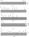
FIG. 1 depicts an inertial andpressure sensor 100 including ahandle layer 102, a buriedoxide layer 104, and adevice layer 106. Anoxide layer 108 separates thedevice layer 106 from acap layer 110. A remainder of apassivation layer 112 is located above thecap layer 110. - Within the
device layer 106, a lowerpressure sensor electrode 114 is defined by twoetch portions etch portions etch portions electrode 114. The lowerpressure sensor electrode 114 is isolated from thecap layer 110 by an etchedportion 120 of theoxide layer 108. Theetched portions cap layer 110 as discussed in more detail below. Sealing of the vent holes provides a closed void including the etchedportions - An upper
pressure sensor electrode 122 is located above the lowerpressure sensor electrode 114 and electrically and mechanically isolated from the lower pressure sensor electrode by the etchedportion 120. The upperpressure sensor electrode 122 is isolated from the rest of thecap layer 110 by twospacers spacers cap layer 110 to the etchedportion 120 and include upper and lower nitride portions, 128 and 130, with anitride gasket portion 132 between the upper and lower nitride portions, 128 and 130. While the description discussesspacers spacers electrode 122. -
Spacers passivation layer 112 to theoxide layer 108, electrically isolate aconnector 138 in thecap layer 110 from the rest of thecap layer 110. Theconnector 138 is in electrical communication with an in-plane electrode portion 140, which is further connected to the lowerpressure sensor electrode 114.Spacer 134 is formed likespacers Spacer 136 is formed having an upper nitride portion 142, and two lower nitride portions 144 with anitride gasket portion 146 between the upper and lower nitride portions, 142 and 144. Aconnector 147 extends from thepassivation layer 112 to thehandle layer 102. Theconnector 147 is defined in thecap layer 110 by thespacer 136 and in the device layer by anisolation post 148.Isolation post 148 extends fromoxide layer 108, beneathspacer 136, through thedevice layer 106, through the buriedoxide layer 104, and into thehandle layer 102. - Within the
device layer 106, a lowerinertial sensor electrode 150 for out-of-plane sensing is defined by two etchedportions etch portions etch portions electrode 150. The lowerinertial sensor electrode 150 is electrically isolated from thecap layer 110 by etchedportions oxide layer 108, except by acontact portion 160. Theetched portions trenches 180 etc. are made with a separate release etching process. This procedure has the advantage, that the sacrificial layer can then also be used as an etch-stop for thetrenches 180, etc. - A
sensing structure 162 for out-of-plane sensing (similar structures can be used for in-plane sensing: counter electrode is then also in-plane similar to sensing structure) is located above the lowerinertial sensor electrode 150, and electrically and mechanically isolated from the lowerinertial sensor electrode 150 by etchedportion 156. Thesensing structure 162 is mechanically and electrically isolated from a portion of thecap layer 110 on one side by etchedportion 166, which extends completely from the upper surface of thecap layer 110 to the etchedportion 156. The etchedportion 166 and aspacer 168, which is formed like thespacers connector 170 in thecap layer 110 from the rest of thecap layer 110. Theconnector 170 is in electrical communication with the lowerinertial sensor electrode 150, via thecontact portion 160. Aspacer 172, which consists of a nitride portion extending from the upper surface of thecap layer 110 to the etchedportion 156, electrically isolates thesensing structure 162 from asensing structure 176, while providing a mechanical coupling thereof. This allows fully differential capacitive sensing/readout. - The
sensing structure 176 provides in-plane or out-of plane sensing and is located in thecap layer 110 and is isolated from thedevice layer 106 by etchedportion 156. Thesensing structure 176 is mechanically and electrically isolated on one side from the rest of thecap layer 110 by etchedportion 180, which extends completely from the upper surface of thecap layer 110 to the etchedportion 156. The etchedportion 180 and aspacer 183, which is formed like thespacers inertial sensor electrode 184 in thecap layer 110 from the rest of thecap layer 110. - A wide etched
portion 188 exposes the upper surface of the cap layer revealingsensing structures portion 190 exposes the upper surface of the cap layer revealing the upperpressure sensor electrode 122. Abond pad 192 is connected through thepassivation layer 112 to the upperinertial sensor electrode 184. Abond pad 194 is connected through thepassivation layer 112 to theconnector 170, which is further connected to the lowerinertial sensor electrode 150. Abond pad 196 is connected through thepassivation layer 112 to theconnector 138, which is further connected to the lowerpressure sensor electrode 114. Abond pad 198 is connected through the passivation layer to theconnector 147. - A process for forming a sensor such as the inertial and
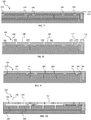
pressure sensor 100 is discussed with reference toFIGs. 2-21 . Referring initially toFIG. 2 , anSOI wafer 200 including ahandle layer 202, a buriedoxide layer 204, and adevice layer 206 is provided and etched with a trench 208 to define aconnector 210. The trench 208 is then filled with atrench nitride portion 212 andtrenches FIG. 3 ). Thetrenches 214 definelower electrode 218 for out-of-plane inertial sensing while thetrenches 216 define alower pressure electrode 220. - The
trench portions trench oxide portion 222 as shown inFIG. 4 using a conformal oxide deposition. The filled trenches define the fixed electrodes in the device layer. While only two are formed in this embodiment, additional electrodes may be defined for particular applications. Oxide deposition further results in anoxide layer 224 on the upper surface of thedevice layer 206. Theoxide layer 224 may be planarized by any desired technique such as chemical mechanical polishing (CMP). - A
trench 226 is etched through theoxide layer 224, thedevice layer 206, and the buriedoxide layer 204 to expose the upper surface of the handle layer 202 (FIG. 5 ). An epi-polysilicon deposition 228 fills the trench 226 (FIG. 6 ) andadditional trenches oxide layer 224. - Referring to
FIG. 7 , an epi-polysilicon deposition fills thecontact openings middle contact portions cap layer portion 254 above theoxide layer 224. A number of trenches are then etched into thecap layer portion 254. Atrench 256 is etched after CMP of the lower cap layer portion 254 (FIG. 8 ). Thetrench 256 extends from the upper surface of the lowercap layer portion 254 to the upper surface of theoxide layer 224 to define anupper electrode 258 for pressure sensing.Trenches inertial sensing portion 266 betweentrenches inertial sensing portion 268 betweentrenches -
Trench 270 is similarly etched to define amiddle contact portion 272, which is connected with lower middle contact portion 250 (seeFIG. 7 ). Finally,trench 274 is similarly etched to define amiddle contact portion 276, which is connected to lower contact portion 228 (seeFIG. 6 ).Trenches trench nitride portions FIG. 9 . - Referring to
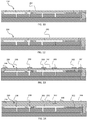
FIG. 10 , after vent holes 290 and 292 are formed, an HF vapor etch release is performed which releases the in-planeinertial sensing portion 266 and the out-of-planeinertial sensing portions 268. The upperpressure sensor electrode 122 is also released by the vapor etch. This step thus sets the corresponding gaps between sensing electrodes and structures. A clean high temperature seal is then performed in an epi-reactor to seal the vent holes 290/292. Alternatively, the vent holes 290/292 may be sealed using oxide, nitride, silicon migration, etc. The resulting configuration is shown inFIG. 11 wherein lowercap layer portion 254 has been reformed after the HF vapor release. - A low
stress nitride layer 292 is then deposited on the upper surface of the lower cap layer portion 254 (FIG. 12 ), and then planarized. Thenitride layer 292 is patterned and etched resulting in the configuration ofFIG. 13 . InFIG. 13 , remainders of thenitride layer 292form gaskets nitride layer 292 form agasket 300 for theupper electrode 258, andgaskets middle contact portion 272 and themiddle contact portion 276. The lateral extent ofgaskets - An epi-polysilicon layer is then formed on the upper surface of the lower
cap layer portion 254 and the upper surface of thegaskets FIG. 14 ). The uppercap layer portion 306 may be planarized if desired. -
Trenches FIG. 15 . Thetrench 308 extends from the upper surface of the uppercap layer portion 306 to the upper surface ofgasket 294 which acts as an etch stop. Thetrench 310 extends from the upper surface of the uppercap layer portion 306 to the upper surface ofgasket 296 which acts as an etch stop. Thetrench 312 extends from the upper surface of the uppercap layer portion 306 to the upper surface ofgasket 298 which acts as an etch stop. Thetrench 314 extends from the upper surface of the uppercap layer portion 306 to the upper surface ofgasket 300 which acts as an etch stop. Thetrench 316 extends from the upper surface of the uppercap layer portion 306 to the upper surface ofgasket 302 which acts as an etch stop. Thetrench 318 extends from the upper surface of the uppercap layer portion 306 to the upper surface ofgasket 304 which acts as an etch stop. - A
nitride passivation layer 320 is then deposited on the upper surface of the uppercap layer portion 306 as shown inFIG. 16 . The deposited nitride also fills thetrenches passivation portions FIG. 16 , in some embodiments a gasket such as thegasket 300 is also provided for thepassivation portion 300. - Contact
openings FIG. 17 ). As shown inFIG. 19 , a metal layer 342 is then deposited on thepassivation layer 320. The metal layer 342 also fills thecontact openings metal contact portions FIG. 19 . InFIG. 19 , a remainder of the metal layer 342 forms abond pad 352 for the in-planeinertial sensing portion 266. A remainder of the metal layer 342 forms abond pad 354 for the out-of-planeinertial sensing portion 268. A remainder of the metal layer 342 forms abond pad 356 for themiddle contact portion 272. A remainder of the metal layer 342 forms abond pad 358 for themiddle contact portion 276. - The
passivation layer 320 is then patterned and etched resulting in the configuration ofFIG 20 . InFIG 20 , wide etchedportion 360 substantially reveals the upper surface of the in-planeinertial sensing portion 266 and the out-of-planeinertial sensing portion 268. There is also a wide etchedportion 362 completely revealing theupper electrode 258 and some of the surrounding portions of the uppercap layer portion 306. - Referring to
FIG. 21 ,trenches cap layer portion 306 and thelower cap layer 254 portion. The structure ofFIG. 21 is the same as the structure of the inertial andpressure sensor 100 ofFIG. 1 . - The above described process may be modified in a number of ways to provide additional features. For example, in embodiments wherein the release of
layer 224 happens in the inertial sensor region after the steps discussed with respect toFIG. 21 , the trench for passivation portion 324 (when there is no gasket associated with the passivation portion 324) can be formed in one single step along with the trenches described with respect toFIG. 15 . - As another example, in some embodiments the
passivation layer 320 is not etched as discussed above with respect toFIG. 20 . Rather, thepassivation layer 320 is left in place in order to protect the pressure sensor, and/or to be used as a hardmask for the inertial sensor patterning discussed above with respect to the trenches ofFIG. 21 . - Moreover, it is sometimes beneficial to have a large structural layer thickness for an inertial sensor area and a lower structural thickness in a pressure sensor area in order to have good sensitivity for both sensors. A pressure sensor membrane is preferably 8-12 µm thick, while the inertial sensor functional layer is preferably 10-40 µm thick.
FIG. 22 depicts an inertial andpressure sensor 400 wherein the effective thickness of apressure sensor membrane 401 has been reduced. - The inertial and
pressure sensor 400 is similar to the inertial andpressure sensor 100, shown inFIG. 1 , and shares all the structural features of the inertial andpressure sensor 100. The difference between the inertial andpressure sensor 400 and the inertial andpressure sensor 100 is that the inertial andpressure sensor 400 has an etched portion 420 (which is corresponds with the etchedportion 120 of the inertial and pressure sensor 100) that further comprises a raisedportion 421. The raisedportion 421 of theetch portion 420 is located at theouter edge 423 of the etchedportion 420 and protrudes into the cap layer 410 (which corresponds with thecap layer 110 of the inertial and pressure sensor 100). The raisedportion 421, as depicted, protrudes roughly halfway through thecap layer 410, but may be designed to modify the effective thickness of the pressure sensor membrane as desired. The reduced thickness of thecap layer 410 about the electrode in the membrane (cap layer 410) effectively reduces the membrane thickness. The raised portions 21 are readily formed simply by etching the cap layer portion 254 (atFIG. 7 ) and depositing additional oxide in the trenches. The remaining process steps are substantially identical. -
FIG. 23 depicts an alternative embodiment in which the effective thickness of the pressure sensor membrane has again been reduced.FIG. 23 depicts an inertial andpressure sensor 600 wherein the effective thickness of apressure sensor membrane 601 has been reduced by etching a deeper wide etched portion 690 (which corresponds with wideetched portion 190 of sensor 100). The inertial andpressure sensor 600 is otherwise similar to the inertial andpressure sensor 100, shown inFIG. 1 , and shares all the other structural features of the inertial andpressure sensor 100. - The inertial and
pressure sensor 600 can be fabricated substantially in the same manner as the inertial andpressure sensor 100. The main difference is that during the deposition of the EPI membrane-layer (i.e., between the configuration ofFIG.s 13 and 14 ), a thin layer of oxide is deposited. This is used as a trench stop during the trench of the inertial sensor structures resulting in the configuration ofFIG. 24 which shows an inertial andpressure sensor 600 with the thin layer ofoxide 709. Using this modification, the membrane thickness can be reduced to the required thickness. Theoxide layer 709 is removed during the release etch of the sensor structures in embodiments wherein the release ofoxide layer 224 happens in the inertial sensor region after the steps discussed above with respect toFIG. 21 , or during a separate release /etch step. Therefore, the process is modified to include only additional steps for oxide deposition and patterning. - In accordance with the above described embodiments, a pressure sensor and an accelerometer are fabricated on a single chip. In some embodiments, a pressures sensor and a gyroscope are fabricated on a single chip. The device of
FIG. 1 can thus be configured as a pressure sensor and an accelerometer, or as a pressure sensor and a gyroscope. By providing another structure substantially like the structure to the left of thesensor electrodes - In some embodiments, a 10-degree of freedom combination chip is fabricated having a 3-axis magnetometer is realized on an application-specific integrated circuit (ASIC), as an add-on chip, or as a Lorentz-force magnetometer in the same process flow as the inertial sensor part on the same MEMS chip.
- In some embodiments, encapsulation is done using wafer-bonding (metallic, eutectic, SLID, glass-frit) with an Si-cap wafer. In other embodiments, the Si-cap wafer of a wafer-bonding encapsulation is an ASIC chip.
- In some embodiments, the chip has a bare-die packaging, and is an ASIC with through-silicon-vias. In some embodiments, the pressure sensor area is not covered by the cap wafer. In some embodiments, the cap wafer has an access port etched into it within the area of the pressure sensor in order to have a pressures port. In some embodiments, the chip has a membrane recess using an oxide layer within the EPI membrane layer as an etch stop. In some embodiments, the membrane has a boss formation using an oxide block formation prior to the membrane deposition.
- While the disclosure has been illustrated and described in detail in the drawings and foregoing description, the same should be considered as illustrative and not restrictive in character. It is understood that only the preferred embodiments have been presented and that all changes, modifications and further applications that come within the spirit of the disclosure are desired to be protected.
Claims (18)
- A MEMS sensor device (100, 400, 600) comprising:a handle layer (102);a device layer (106) located above the handle layer (102);a first fixed electrode (114) defined in the device layer (106);a second fixed electrode (150) defined in the device layer (106) and electrically isolated from the first fixed electrode (114);a cap layer (110) located above the device layer (106);a first movable electrode (122, 401, 601) defined in the cap layer (110) at a location directly above the first fixed electrode (114);a second movable electrode (184) defined in the cap layer (110), at least partially directly above the second fixed electrode (150), and electrically isolated from the first movable electrode (122, 401, 601);a first void (120, 420) located directly between the first fixed electrode (114) and the first movable electrode (122, 401, 601), the first void (120, 420) sealed from an atmosphere above the cap layer (110); anda second void (156, 158) located directly between the second fixed electrode (150) and the second movable electrode (184), the second void open (156, 158) to the atmosphere.
- The MEMS sensor device (400, 600) of claim 1, wherein:a first portion of the cap layer (110) supporting the first movable electrode (401, 601) has a first minimum thickness;a second portion of the cap layer (110) supporting the second movable electrode (184) has a second minimum thickness; andthe first minimum thickness is less than the second minimum thickness.
- The MEMS sensor device (400) of claim 2, wherein a maximum thickness of the first movable electrode (401) is substantially identical to a maximum thickness of the second movable electrode (184).
- The MEMS sensor device (400) of claim 3 the first void (420) comprising:a first void portion positioned directly between the first fixed electrode (114) and the first movable electrode (401); anda second void portion (421) extending upwardly from the first void portion into the cap layer (110).
- The MEMS sensor device (600) of claim 2, wherein a maximum thickness of the first movable electrode (601) is less than a maximum thickness of the second movable electrode (184).
- The MEMS sensor device (600) of claim 5, wherein an uppermost surface of the first movable electrode (601) is below an uppermost surface of the second movable electrode (184).
- The MEMS sensor device (100, 400, 600) of claim 1, wherein the first movable electrode (122, 401, 601) is defined at least in part by:a first nitride portion (130) extending vertically upwardly from a portion of the first void (120, 420); anda second nitride portion (132) extending horizontally from the first nitride portion (130).
- The MEMS sensor device (100, 400, 600) of claim 7, wherein the first movable electrode (122, 401, 601) is further defined at least in part by:a third nitride portion (128) extending vertically upwardly from the second nitride portion (132).
- The MEMS sensor device (100, 400, 600) of claim 7, wherein the second movable electrode (184) comprises:a first movable electrode portion (162) directly above the second fixed electrode (150);a second movable electrode portion (176) horizontally offset from the second fixed electrode (150); anda nitride spacer (172) electrically isolating the first movable electrode portion (162) from the second movable electrode portion (176), the MEMS sensor device (100, 400, 600) further including:
a third fixed electrode (170) defined in the cap layer (110) adjacent to the second movable electrode portion (176). - The MEMS sensor device (100, 400, 600) of claim 1, wherein:the first fixed electrode (114) and the first movable electrode (122, 401, 601) are configured as a pressure sensor; andthe second fixed electrode (150) and the second movable electrode (184) are configured as a gyroscope sensor.
- The MEMS sensor device (100, 400, 600) of claim 1, wherein:the first fixed electrode (114) and the first movable electrode (122, 401, 601) are configured as a pressure sensor; andthe second fixed electrode (150) and the second movable electrode (184) are configured as an accelerometer sensor.
- A method of forming a MEMS sensor device (100, 400, 600), comprising:defining a first fixed electrode (114) in a device layer (106) located above a handle layer (102);defining a second fixed electrode (150) in the device layer (106) at the same time that the first fixed electrode (114) is defined;defining a first movable electrode (122, 401, 601) in a cap layer (110) above the device layer (106), the first movable electrode (122, 401, 601) at a location directly above the first fixed electrode (114);defining a second movable electrode (184) in the cap layer (110), the second movable electrode (184) at least partially directly above the second fixed electrode (150), and electrically isolated from the first movable electrode (122, 401, 601);releasing the first movable electrode (122, 401, 601) from the device layer (106) by forming a first void (120, 420);sealing the first void (120, 420) from an atmosphere above the cap layer (110);releasing the second movable electrode (184) from the device layer (106) by forming a second void (156, 158); andopening the second void (156, 158) to the atmosphere.
- The method of claim 12, wherein releasing the second movable electrode (184) occurs during the same process step as releasing the first movable electrode (122, 401, 601).
- The method of claim 12, wherein releasing the second movable electrode (184) occurs during a process step subsequent to releasing the first movable electrode (122, 401, 601).
- The method of claim 12, further comprising:isolating a first portion (162) of the second movable electrode (184) from a second portion (176) of the second movable electrode (184), wherein the first portion (162) is directly above the second fixed electrode (150); anddefining a third fixed electrode (170) in the cap layer at a location adjacent to the second portion (176).
- The method of claim 12, wherein defining a first movable electrode (122, 401, 601) comprises:forming a lower nitride portion (130) within the cap layer (110), the lower nitride portion (130) extending upwardly from a buried oxide layer (108);forming a gasket portion (132) above the lower nitride portion (130); andforming an upper nitride portion (128) within the cap layer (110), the upper nitride portion (128) extending upwardly from the gasket (132).
- The method of claim 12, further comprising:
etching a portion of the cap layer (110) directly above the defined first movable electrode (601) to provide a reduced thickness membrane in which the first movable electrode (601) is defined. - The method of claim 12, wherein releasing the first movable electrode (401) from the device layer (106) comprises:forming a first void portion located directly between the defined first fixed electrode (114) and the defined first movable electrode (401); andforming a second void portion (421) extending upwardly from the first void portion within the cap layer (110).
Applications Claiming Priority (2)
| Application Number | Priority Date | Filing Date | Title |
|---|---|---|---|
| US201361862370P | 2013-08-05 | 2013-08-05 | |
| PCT/US2014/049210 WO2015020881A1 (en) | 2013-08-05 | 2014-07-31 | Inertial and pressure sensors on single chip |
Publications (3)
| Publication Number | Publication Date |
|---|---|
| EP3030875A1 EP3030875A1 (en) | 2016-06-15 |
| EP3030875A4 EP3030875A4 (en) | 2017-01-11 |
| EP3030875B1 true EP3030875B1 (en) | 2018-05-23 |
Family
ID=52426909
Family Applications (1)
| Application Number | Title | Priority Date | Filing Date |
|---|---|---|---|
| EP14834662.0A Active EP3030875B1 (en) | 2013-08-05 | 2014-07-31 | Inertial and pressure sensors on single chip |
Country Status (5)
| Country | Link |
|---|---|
| US (1) | US9194882B2 (en) |
| EP (1) | EP3030875B1 (en) |
| CN (1) | CN105874312B (en) |
| TW (1) | TWI624954B (en) |
| WO (1) | WO2015020881A1 (en) |
Families Citing this family (9)
| Publication number | Priority date | Publication date | Assignee | Title |
|---|---|---|---|---|
| CN105264859B (en) * | 2013-04-09 | 2018-08-31 | 诺基亚通信公司 | For generating the method and apparatus known clearly to the customer experience of the application based on web |
| US9749902B2 (en) * | 2014-08-19 | 2017-08-29 | Qualcomm Incorporated | Admission control and load balancing |
| JP6868963B2 (en) * | 2016-03-15 | 2021-05-12 | エイブリック株式会社 | Magnetic sensor and its manufacturing method |
| CN107758606B (en) * | 2016-08-19 | 2020-01-24 | 上海丽恒光微电子科技有限公司 | Packaging method of pressure sensor |
| GB2575690A (en) * | 2018-07-20 | 2020-01-22 | Gillespie Avionics Ltd | Liquid measurement device for a tank |
| DE102019202794B3 (en) * | 2019-03-01 | 2019-11-07 | Robert Bosch Gmbh | Micromechanical sensor device and corresponding manufacturing method |
| CN111208317B (en) * | 2020-02-26 | 2021-07-02 | 深迪半导体(绍兴)有限公司 | MEMS inertial sensor, application method and electronic equipment |
| DE102020123160B3 (en) | 2020-09-04 | 2021-10-14 | Infineon Technologies Dresden GmbH & Co. KG | Semiconductors with pressure and acceleration sensor elements |
| CN116374942B (en) * | 2023-06-07 | 2023-08-04 | 苏州敏芯微电子技术股份有限公司 | Microelectromechanical component integrating inertial and pressure sensors |
Family Cites Families (14)
| Publication number | Priority date | Publication date | Assignee | Title |
|---|---|---|---|---|
| US20050172717A1 (en) * | 2004-02-06 | 2005-08-11 | General Electric Company | Micromechanical device with thinned cantilever structure and related methods |
| US20080277746A1 (en) * | 2004-10-21 | 2008-11-13 | Sharp Laboratories Of America, Inc. | Nanowire sensor with self-aligned electrode support |
| US7518493B2 (en) * | 2005-12-01 | 2009-04-14 | Lv Sensors, Inc. | Integrated tire pressure sensor system |
| DE102009029217A1 (en) * | 2009-09-04 | 2011-03-10 | Robert Bosch Gmbh | Inertial sensor with a field effect transistor |
| US8387464B2 (en) | 2009-11-30 | 2013-03-05 | Freescale Semiconductor, Inc. | Laterally integrated MEMS sensor device with multi-stimulus sensing |
| US8569092B2 (en) * | 2009-12-28 | 2013-10-29 | General Electric Company | Method for fabricating a microelectromechanical sensor with a piezoresistive type readout |
| US8216882B2 (en) * | 2010-08-23 | 2012-07-10 | Freescale Semiconductor, Inc. | Method of producing a microelectromechanical (MEMS) sensor device |
| JP5649474B2 (en) | 2011-01-26 | 2015-01-07 | ローム株式会社 | Capacitance type pressure sensor and method of manufacturing capacitance type pressure sensor |
| CN102180435B (en) * | 2011-03-15 | 2012-10-10 | 迈尔森电子(天津)有限公司 | Integrated micro electro-mechanical system (MEMS) device and forming method thereof |
| CN102183677B (en) * | 2011-03-15 | 2012-08-08 | 迈尔森电子(天津)有限公司 | Integrated inertial sensor and pressure sensor and forming method thereof |
| US8673756B2 (en) * | 2011-04-14 | 2014-03-18 | Robert Bosch Gmbh | Out-of-plane spacer defined electrode |
| CN102249177B (en) * | 2011-05-18 | 2014-02-05 | 上海丽恒光微电子科技有限公司 | Micro-electromechanical sensor and forming method thereof |
| JP5541306B2 (en) | 2011-05-27 | 2014-07-09 | 株式会社デンソー | Mechanical quantity sensor device and manufacturing method thereof |
| US9040355B2 (en) * | 2012-07-11 | 2015-05-26 | Freescale Semiconductor, Inc. | Sensor package and method of forming same |
-
2014
- 2014-07-31 US US14/447,696 patent/US9194882B2/en active Active
- 2014-07-31 EP EP14834662.0A patent/EP3030875B1/en active Active
- 2014-07-31 WO PCT/US2014/049210 patent/WO2015020881A1/en active Application Filing
- 2014-07-31 CN CN201480054655.5A patent/CN105874312B/en active Active
- 2014-08-04 TW TW103126556A patent/TWI624954B/en active
Non-Patent Citations (1)
| Title |
|---|
| None * |
Also Published As
| Publication number | Publication date |
|---|---|
| EP3030875A4 (en) | 2017-01-11 |
| WO2015020881A1 (en) | 2015-02-12 |
| CN105874312B (en) | 2019-04-12 |
| TW201515240A (en) | 2015-04-16 |
| US9194882B2 (en) | 2015-11-24 |
| TWI624954B (en) | 2018-05-21 |
| EP3030875A1 (en) | 2016-06-15 |
| CN105874312A (en) | 2016-08-17 |
| US20150035093A1 (en) | 2015-02-05 |
Similar Documents
| Publication | Publication Date | Title |
|---|---|---|
| EP3030875B1 (en) | Inertial and pressure sensors on single chip | |
| EP3052901B1 (en) | Inertial and pressure sensors on single chip | |
| US9518877B2 (en) | Micromechanical component for a capacitive sensor device, and manufacturing method for a micromechanical component for a capacitive sensor device | |
| EP2697159B1 (en) | Out-of-plane spacer defined electrode | |
| EP1633673B1 (en) | Method for fabricating microelectromechanical systems having trench isolated contacts | |
| EP1652219B1 (en) | Anchors for microelectromechanical systems having an soi substrate, and method of fabricating same | |
| US7671515B2 (en) | Microelectromechanical devices and fabrication methods | |
| US10173887B2 (en) | Epi-poly etch stop for out of plane spacer defined electrode | |
| EP2943435B1 (en) | Cmos integrated moving-gate transducer with silicon as a functional layer | |
| KR20170004123A (en) | Sensor element and method for manufacturing same | |
| JP6282227B2 (en) | Method for forming a wide trench using a sacrificial slab | |
| US8430255B2 (en) | Method of accurately spacing Z-axis electrode | |
| TWI528566B (en) | Method and structure of monolithically integrated absolute pressure sensor |
Legal Events
| Date | Code | Title | Description |
|---|---|---|---|
| PUAI | Public reference made under article 153(3) epc to a published international application that has entered the european phase |
Free format text: ORIGINAL CODE: 0009012 |
|
| 17P | Request for examination filed |
Effective date: 20160307 |
|
| AK | Designated contracting states |
Kind code of ref document: A1 Designated state(s): AL AT BE BG CH CY CZ DE DK EE ES FI FR GB GR HR HU IE IS IT LI LT LU LV MC MK MT NL NO PL PT RO RS SE SI SK SM TR |
|
| AX | Request for extension of the european patent |
Extension state: BA ME |
|
| DAX | Request for extension of the european patent (deleted) | ||
| A4 | Supplementary search report drawn up and despatched |
Effective date: 20161208 |
|
| RIC1 | Information provided on ipc code assigned before grant |
Ipc: G01P 15/08 20060101ALI20161202BHEP Ipc: G01L 9/12 20060101AFI20161202BHEP Ipc: G01P 15/125 20060101ALI20161202BHEP Ipc: B81B 7/02 20060101ALI20161202BHEP Ipc: G01P 1/02 20060101ALI20161202BHEP Ipc: G01P 15/18 20130101ALI20161202BHEP |
|
| GRAP | Despatch of communication of intention to grant a patent |
Free format text: ORIGINAL CODE: EPIDOSNIGR1 |
|
| INTG | Intention to grant announced |
Effective date: 20180202 |
|
| GRAS | Grant fee paid |
Free format text: ORIGINAL CODE: EPIDOSNIGR3 |
|
| GRAA | (expected) grant |
Free format text: ORIGINAL CODE: 0009210 |
|
| AK | Designated contracting states |
Kind code of ref document: B1 Designated state(s): AL AT BE BG CH CY CZ DE DK EE ES FI FR GB GR HR HU IE IS IT LI LT LU LV MC MK MT NL NO PL PT RO RS SE SI SK SM TR |
|
| REG | Reference to a national code |
Ref country code: GB Ref legal event code: FG4D |
|
| REG | Reference to a national code |
Ref country code: CH Ref legal event code: EP |
|
| REG | Reference to a national code |
Ref country code: IE Ref legal event code: FG4D |
|
| REG | Reference to a national code |
Ref country code: AT Ref legal event code: REF Ref document number: 1001894 Country of ref document: AT Kind code of ref document: T Effective date: 20180615 |
|
| REG | Reference to a national code |
Ref country code: DE Ref legal event code: R096 Ref document number: 602014025975 Country of ref document: DE |
|
| REG | Reference to a national code |
Ref country code: NL Ref legal event code: MP Effective date: 20180523 |
|
| REG | Reference to a national code |
Ref country code: LT Ref legal event code: MG4D |
|
| PG25 | Lapsed in a contracting state [announced via postgrant information from national office to epo] |
Ref country code: LT Free format text: LAPSE BECAUSE OF FAILURE TO SUBMIT A TRANSLATION OF THE DESCRIPTION OR TO PAY THE FEE WITHIN THE PRESCRIBED TIME-LIMIT Effective date: 20180523 Ref country code: FI Free format text: LAPSE BECAUSE OF FAILURE TO SUBMIT A TRANSLATION OF THE DESCRIPTION OR TO PAY THE FEE WITHIN THE PRESCRIBED TIME-LIMIT Effective date: 20180523 Ref country code: SE Free format text: LAPSE BECAUSE OF FAILURE TO SUBMIT A TRANSLATION OF THE DESCRIPTION OR TO PAY THE FEE WITHIN THE PRESCRIBED TIME-LIMIT Effective date: 20180523 Ref country code: NO Free format text: LAPSE BECAUSE OF FAILURE TO SUBMIT A TRANSLATION OF THE DESCRIPTION OR TO PAY THE FEE WITHIN THE PRESCRIBED TIME-LIMIT Effective date: 20180823 Ref country code: ES Free format text: LAPSE BECAUSE OF FAILURE TO SUBMIT A TRANSLATION OF THE DESCRIPTION OR TO PAY THE FEE WITHIN THE PRESCRIBED TIME-LIMIT Effective date: 20180523 Ref country code: BG Free format text: LAPSE BECAUSE OF FAILURE TO SUBMIT A TRANSLATION OF THE DESCRIPTION OR TO PAY THE FEE WITHIN THE PRESCRIBED TIME-LIMIT Effective date: 20180823 |
|
| PG25 | Lapsed in a contracting state [announced via postgrant information from national office to epo] |
Ref country code: NL Free format text: LAPSE BECAUSE OF FAILURE TO SUBMIT A TRANSLATION OF THE DESCRIPTION OR TO PAY THE FEE WITHIN THE PRESCRIBED TIME-LIMIT Effective date: 20180523 Ref country code: RS Free format text: LAPSE BECAUSE OF FAILURE TO SUBMIT A TRANSLATION OF THE DESCRIPTION OR TO PAY THE FEE WITHIN THE PRESCRIBED TIME-LIMIT Effective date: 20180523 Ref country code: HR Free format text: LAPSE BECAUSE OF FAILURE TO SUBMIT A TRANSLATION OF THE DESCRIPTION OR TO PAY THE FEE WITHIN THE PRESCRIBED TIME-LIMIT Effective date: 20180523 Ref country code: GR Free format text: LAPSE BECAUSE OF FAILURE TO SUBMIT A TRANSLATION OF THE DESCRIPTION OR TO PAY THE FEE WITHIN THE PRESCRIBED TIME-LIMIT Effective date: 20180824 Ref country code: LV Free format text: LAPSE BECAUSE OF FAILURE TO SUBMIT A TRANSLATION OF THE DESCRIPTION OR TO PAY THE FEE WITHIN THE PRESCRIBED TIME-LIMIT Effective date: 20180523 |
|
| REG | Reference to a national code |
Ref country code: AT Ref legal event code: MK05 Ref document number: 1001894 Country of ref document: AT Kind code of ref document: T Effective date: 20180523 |
|
| PG25 | Lapsed in a contracting state [announced via postgrant information from national office to epo] |
Ref country code: AT Free format text: LAPSE BECAUSE OF FAILURE TO SUBMIT A TRANSLATION OF THE DESCRIPTION OR TO PAY THE FEE WITHIN THE PRESCRIBED TIME-LIMIT Effective date: 20180523 Ref country code: EE Free format text: LAPSE BECAUSE OF FAILURE TO SUBMIT A TRANSLATION OF THE DESCRIPTION OR TO PAY THE FEE WITHIN THE PRESCRIBED TIME-LIMIT Effective date: 20180523 Ref country code: DK Free format text: LAPSE BECAUSE OF FAILURE TO SUBMIT A TRANSLATION OF THE DESCRIPTION OR TO PAY THE FEE WITHIN THE PRESCRIBED TIME-LIMIT Effective date: 20180523 Ref country code: RO Free format text: LAPSE BECAUSE OF FAILURE TO SUBMIT A TRANSLATION OF THE DESCRIPTION OR TO PAY THE FEE WITHIN THE PRESCRIBED TIME-LIMIT Effective date: 20180523 Ref country code: CZ Free format text: LAPSE BECAUSE OF FAILURE TO SUBMIT A TRANSLATION OF THE DESCRIPTION OR TO PAY THE FEE WITHIN THE PRESCRIBED TIME-LIMIT Effective date: 20180523 Ref country code: SK Free format text: LAPSE BECAUSE OF FAILURE TO SUBMIT A TRANSLATION OF THE DESCRIPTION OR TO PAY THE FEE WITHIN THE PRESCRIBED TIME-LIMIT Effective date: 20180523 Ref country code: PL Free format text: LAPSE BECAUSE OF FAILURE TO SUBMIT A TRANSLATION OF THE DESCRIPTION OR TO PAY THE FEE WITHIN THE PRESCRIBED TIME-LIMIT Effective date: 20180523 |
|
| REG | Reference to a national code |
Ref country code: DE Ref legal event code: R097 Ref document number: 602014025975 Country of ref document: DE |
|
| PG25 | Lapsed in a contracting state [announced via postgrant information from national office to epo] |
Ref country code: SM Free format text: LAPSE BECAUSE OF FAILURE TO SUBMIT A TRANSLATION OF THE DESCRIPTION OR TO PAY THE FEE WITHIN THE PRESCRIBED TIME-LIMIT Effective date: 20180523 Ref country code: IT Free format text: LAPSE BECAUSE OF FAILURE TO SUBMIT A TRANSLATION OF THE DESCRIPTION OR TO PAY THE FEE WITHIN THE PRESCRIBED TIME-LIMIT Effective date: 20180523 |
|
| REG | Reference to a national code |
Ref country code: CH Ref legal event code: PL |
|
| PG25 | Lapsed in a contracting state [announced via postgrant information from national office to epo] |
Ref country code: LU Free format text: LAPSE BECAUSE OF NON-PAYMENT OF DUE FEES Effective date: 20180731 Ref country code: MC Free format text: LAPSE BECAUSE OF FAILURE TO SUBMIT A TRANSLATION OF THE DESCRIPTION OR TO PAY THE FEE WITHIN THE PRESCRIBED TIME-LIMIT Effective date: 20180523 |
|
| PLBE | No opposition filed within time limit |
Free format text: ORIGINAL CODE: 0009261 |
|
| STAA | Information on the status of an ep patent application or granted ep patent |
Free format text: STATUS: NO OPPOSITION FILED WITHIN TIME LIMIT |
|
| REG | Reference to a national code |
Ref country code: BE Ref legal event code: MM Effective date: 20180731 |
|
| GBPC | Gb: european patent ceased through non-payment of renewal fee |
Effective date: 20180823 |
|
| PG25 | Lapsed in a contracting state [announced via postgrant information from national office to epo] |
Ref country code: LI Free format text: LAPSE BECAUSE OF NON-PAYMENT OF DUE FEES Effective date: 20180731 Ref country code: FR Free format text: LAPSE BECAUSE OF NON-PAYMENT OF DUE FEES Effective date: 20180731 Ref country code: CH Free format text: LAPSE BECAUSE OF NON-PAYMENT OF DUE FEES Effective date: 20180731 |
|
| 26N | No opposition filed |
Effective date: 20190226 |
|
| REG | Reference to a national code |
Ref country code: IE Ref legal event code: MM4A |
|
| PG25 | Lapsed in a contracting state [announced via postgrant information from national office to epo] |
Ref country code: SI Free format text: LAPSE BECAUSE OF FAILURE TO SUBMIT A TRANSLATION OF THE DESCRIPTION OR TO PAY THE FEE WITHIN THE PRESCRIBED TIME-LIMIT Effective date: 20180523 Ref country code: BE Free format text: LAPSE BECAUSE OF NON-PAYMENT OF DUE FEES Effective date: 20180731 |
|
| PG25 | Lapsed in a contracting state [announced via postgrant information from national office to epo] |
Ref country code: IE Free format text: LAPSE BECAUSE OF NON-PAYMENT OF DUE FEES Effective date: 20180731 |
|
| PG25 | Lapsed in a contracting state [announced via postgrant information from national office to epo] |
Ref country code: GB Free format text: LAPSE BECAUSE OF NON-PAYMENT OF DUE FEES Effective date: 20180823 |
|
| PG25 | Lapsed in a contracting state [announced via postgrant information from national office to epo] |
Ref country code: AL Free format text: LAPSE BECAUSE OF FAILURE TO SUBMIT A TRANSLATION OF THE DESCRIPTION OR TO PAY THE FEE WITHIN THE PRESCRIBED TIME-LIMIT Effective date: 20180523 |
|
| PG25 | Lapsed in a contracting state [announced via postgrant information from national office to epo] |
Ref country code: MT Free format text: LAPSE BECAUSE OF NON-PAYMENT OF DUE FEES Effective date: 20180731 |
|
| PG25 | Lapsed in a contracting state [announced via postgrant information from national office to epo] |
Ref country code: TR Free format text: LAPSE BECAUSE OF FAILURE TO SUBMIT A TRANSLATION OF THE DESCRIPTION OR TO PAY THE FEE WITHIN THE PRESCRIBED TIME-LIMIT Effective date: 20180523 |
|
| PG25 | Lapsed in a contracting state [announced via postgrant information from national office to epo] |
Ref country code: PT Free format text: LAPSE BECAUSE OF FAILURE TO SUBMIT A TRANSLATION OF THE DESCRIPTION OR TO PAY THE FEE WITHIN THE PRESCRIBED TIME-LIMIT Effective date: 20180523 |
|
| PG25 | Lapsed in a contracting state [announced via postgrant information from national office to epo] |
Ref country code: HU Free format text: LAPSE BECAUSE OF FAILURE TO SUBMIT A TRANSLATION OF THE DESCRIPTION OR TO PAY THE FEE WITHIN THE PRESCRIBED TIME-LIMIT; INVALID AB INITIO Effective date: 20140731 Ref country code: CY Free format text: LAPSE BECAUSE OF FAILURE TO SUBMIT A TRANSLATION OF THE DESCRIPTION OR TO PAY THE FEE WITHIN THE PRESCRIBED TIME-LIMIT Effective date: 20180523 Ref country code: MK Free format text: LAPSE BECAUSE OF NON-PAYMENT OF DUE FEES Effective date: 20180523 |
|
| PG25 | Lapsed in a contracting state [announced via postgrant information from national office to epo] |
Ref country code: IS Free format text: LAPSE BECAUSE OF FAILURE TO SUBMIT A TRANSLATION OF THE DESCRIPTION OR TO PAY THE FEE WITHIN THE PRESCRIBED TIME-LIMIT Effective date: 20180923 |
|
| PGFP | Annual fee paid to national office [announced via postgrant information from national office to epo] |
Ref country code: DE Payment date: 20230922 Year of fee payment: 10 |