EP1560353A2 - Konverter für Satellitenrundfunk, und darin verwendete Detektorschaltung - Google Patents
Konverter für Satellitenrundfunk, und darin verwendete Detektorschaltung Download PDFInfo
- Publication number
- EP1560353A2 EP1560353A2 EP05001714A EP05001714A EP1560353A2 EP 1560353 A2 EP1560353 A2 EP 1560353A2 EP 05001714 A EP05001714 A EP 05001714A EP 05001714 A EP05001714 A EP 05001714A EP 1560353 A2 EP1560353 A2 EP 1560353A2
- Authority
- EP
- European Patent Office
- Prior art keywords
- circuit
- phase
- pulse signal
- signal
- switching pulse
- Prior art date
- Legal status (The legal status is an assumption and is not a legal conclusion. Google has not performed a legal analysis and makes no representation as to the accuracy of the status listed.)
- Withdrawn
Links
Images

Classifications
-
- H—ELECTRICITY
- H04—ELECTRIC COMMUNICATION TECHNIQUE
- H04H—BROADCAST COMMUNICATION
- H04H40/00—Arrangements specially adapted for receiving broadcast information
- H04H40/18—Arrangements characterised by circuits or components specially adapted for receiving
- H04H40/27—Arrangements characterised by circuits or components specially adapted for receiving specially adapted for broadcast systems covered by groups H04H20/53 - H04H20/95
- H04H40/90—Arrangements characterised by circuits or components specially adapted for receiving specially adapted for broadcast systems covered by groups H04H20/53 - H04H20/95 specially adapted for satellite broadcast receiving
Definitions
- the present invention relates to a converter, called a broadcasting satellite (BS) converter in this field, which is used to receive BS signals in a satellite broadcasting system, and more particularly relates to an improvement of a control circuit incorporated in the BS converter to select either a high frequency band or a low frequency band included in a reception frequency band used in the satellite broadcasting system.
- BS broadcasting satellite
- the widened reception frequency band is defined as one between 10.7 GHz and 12.75 GHz, and it is impossible to receive all broadcasting satellite (BS) signals (microwaves), included in the widen reception frequency band, with only one parabola antenna and one BS converter. In other words, it is necessary to prepare two parabola antennas and two BS converters before all the BS signals can be received.
- BS broadcasting satellite
- the reception frequency band is divided into a low frequency band of 10.7 GHz to 11.7 GHz and a high frequency band of 11.7 GHz to 12.75 GHz, and the two parabola antennas and two BS converters are arranged for the respective low and high frequency bands.
- JP-A-H08-293812 corresponding to U.S. Patent No. 5,649,311, discloses a prior art BS converter which is constituted so as to receive all the BS signals included in the reception frequency band. Namely, according to JP-A-H08-293812, it is possible to receive all the BS signals with a single parabola antenna and BS converter.
- This prior art BS converter is provided with a reception circuit for receiving all the BS signals, and a control circuit for controlling the reception circuit.
- the reception circuit includes a mixer, and first and second local oscillators connected to the mixer.
- the first local oscillator inputs a first local frequency signal to the mixer, and the second local oscillator inputs a second local frequency signal to the mixer.
- the first local frequency signal features a lower frequency than that of the second local frequency signal.
- the control circuit selects which local oscillator should be driven.
- a television set which is connected to the BS converter through the intermediary of a broadcasting satellite (BS) and a coaxial cable, is tuned to a channel to receive a BS signal included in the low frequency band of 10.7 GHz to 11.7 GHz
- BS broadcasting satellite
- the first local oscillator is driven by the control circuit so that the BS signals included in the low frequency band of 10.7 GHz to 11.7 GHz are converted into intermediate frequency signals featuring a frequency of 950 MHz to 2150 MHz.
- the television set is tuned to a channel to receive a BS signal included in the high frequency band of 11.7 GHz to 12.75 GHz
- only the second local oscillator is driven by the control circuit so that the BS signals included in the high frequency band of 11.7 GHz to 12.75 GHz are converted into intermediate frequency signals featuring a frequency of 950 MHz to 2150 MHz.
- the prior art BS converter it is possible to receive all the BS signals by the single parabola antenna and BS converter. Nevertheless; the prior art BS converter is not satisfactory in that it is impossible to obtain reliable operation.
- a band switching pulse signal is superimposed on a power supply voltage signal which is fed from the BS tuner to the BS converter through the coaxial cable.
- the control circuit includes a detector circuit for detecting whether the band switching pulse signal is superimposed on the power supply voltage signal, and a selector circuit for selectively driving the second local oscillator when the band switching pulse signal is detected by the detector circuit.
- the detector circuit is susceptible to large amplitude noise, such as a spike noise or the like. As a result, a malfunction of the detector circuit may occur. Namely, the control circuit may mistakenly select which local oscillator should be driven, as explained in detail hereinafter.
- an object of the present invention is to provide a broadcasting satellite (BS) converter used to receive BS signals in a satellite broadcasting system, which is constituted such that it is possible to obtain a satisfactory reliable operation.
- BS broadcasting satellite
- Another object of the present invention is to provide a detector circuit used in such a BS converter, which is not susceptible to various noises.
- Yet another object of the present invention is to provide a control circuit that controls a receiver circuit included in such a BS converter.
- a broadcasting satellite (BS) converter adapted to be connected to a broadcasting satellite tuner and fed with a pulse signal from the broadcasting satellite tuner.
- the BS converter comprises a receiver circuit including a mixer, and a plurality of local oscillators connected to the mixer to convert broadcasting satellite signals into intermediate frequency signals.
- the BS converter further comprises a control circuit that controls the receiver circuit.
- the control circuit includes a detector circuit that detects whether a band switching pulse signal is superimposed on the pulse signal, and the detector circuit includes a phase-lock loop circuit for the detection of the band switching pulse signal.
- the control circuit further includes a selector circuit that selectively drives one of the local oscillators in accordance with a detection result obtained in the detector circuit.
- the detector circuit may further include a high pass filter that is constituted such that the band switching pulse signal is allowed to pass therethrough, a level detector circuit that detects a peak voltage of the band switching pulse signal so as to wave-shape the band switching pulse signal, the wave-shaped band switching pulse signal being input to the phase-lock loop circuit.
- the level detector circuit includes a comparator featuring a hysteresis characteristic for the wave-shaping of the band switching pulse signal.
- the phase-locked loop circuit may include a free-running oscillation type voltage control oscillator that outputs an oscillation signal having a frequency which is near to a frequency of the band switching pulse signal, a phase detector that compares a phase of the band switching pulse signal with a phase of the oscillation signal to thereby detect a phase difference therebetween, and a loop filter that outputs a voltage signal in accordance with the phase difference.
- the voltage signal is fed back to the free-running oscillation type voltage control oscillator such that a locked state is established in the phase-locked loop circuit.
- the detector circuit may further include a comparator circuit that compares the voltage signal, output from the loop filter, with a reference voltage, to thereby detect whether the locked state is established in the phase-locked loop circuit.
- the comparator circuit includes a variable voltage sources that varies the reference voltage.
- the phase-locked loop circuit may further include a 180°-phase shifter that produces a 180°-phase-shifted oscillation signal from the oscillation signal.
- the 180°-phase-shifted oscillation signal is input to the phase detector to thereby establish the locked state in which the phase of the band switching pulse signal is advanced or retarded by 90° with respect to the phase of the oscillation signal.
- the phase detector may be constituted as a double-balanced-multiplier.
- the detector circuit may further include a window-type comparator circuit that compares the voltage signal, output from the loop filter, with a first predetermined reference voltage and a second predetermined reference voltage to thereby detect whether the locked state is established in the phase-locked loop circuit.
- the window-type comparator circuit includes a first variable voltage sources that varies the first reference voltage, and a second variable voltage source that varies the second reference voltage.
- a detector circuit that detects whether a band switching pulse signal is superimposed on a power supply voltage signal fed from a broadcasting satellite tuner to a receiver circuit of a broadcasting satellite converter.
- the detector circuit comprises a phase locked loop circuit that is constituted such that a locked state is established when the band switching pulse signal is input thereto.
- the detector circuit may further comprise a high pass filter that is constituted such that the band switching pulse signal is allowed to pass therethrough, and a level detector circuit that detects a peak voltage of the band switching pulse signal so as to wave-shape the band switching pulse signal, with the wave-shaped band switching pulse signal being input to the phase locked loop circuit.
- a control circuit that controls a plurality of local oscillators, included in a receiver circuit of a broadcasting satellite converter, with a band switching pulse signal superimposed on a pulse signal fed from a broadcasting satellite tuner to the receiver circuit.
- the control circuit comprises a detector circuit that detects whether the band switching pulse signal is superimposed on the pulse signal, the detector circuit including a phase locked loop circuit that is constituted such that a locked state is established when the band switching pulse signal is input thereto, and a selector circuit that selectively drives one of the local oscillators in accordance with a detection result obtained in the detector circuit.
- This prior art BS converter is provided with a feed horn 12 associated with an exterior parabola antenna (not shown), and is connected to an interior broadcasting satellite (BS) tuner 14 through a coaxial cable 16.
- BS broadcasting satellite
- the BS converter 10 comprises a power source circuit 18, a receiver circuit 20, a control circuit 22, and a selector circuit 24.
- a power supply voltage signal is fed from the BS tuner 14 to the BS converter 10 through the coaxial cable 16, and is input to the power source circuit 18 and the selector circuit 24.
- the power supply voltage signal is switched between a low voltage (e.g. 13 volts) and a high voltage (e.g. 18 volts) for the reasons stated in detail hereinafter, the power source circuit 18 always generates a constant power supply voltage (e.g. 4 volts) for operating the receiver circuit 20, the control circuit 22, and the selector circuit 24.
- the receiver circuit 20 includes a set of first and second primary amplifiers 26V and 26H, a secondary amplifier 28, a mixer 30, a set of first and second local oscillators 32L and 32H, and an amplifier 34.
- Broadcasting satellite (BS) signals (microwaves), which are transmitted from a satellite, are converged on the feed horn 12 by the parabola antenna, and each of the BS signals is separated into a vertically polarized wave and a horizontally polarized wave.
- the vertically-polarized waves are fed to the first primary amplifier 26V, and are amplified and output to the secondary amplifier 28 as BS signals featuring the vertical polarization.
- the horizontally-polarized waves are fed to the second primary amplifier 26H, and are amplified and output to the secondary amplifier 28 as BS signals featuring the horizontal polarization.
- the BS signals are included in a widened reception frequency band which is defined as one between 10.7 GHz and 12.75 GHz.
- the power supply voltage signal input to the selector switch 24, is switched from the high voltage (18 volts) to the low voltage (13 volts).
- a first drive control signal which is output from the selector circuit 24 to the first primary amplifier 26V
- a second drive control signal which is output from the selector circuit 24 to the second primary amplifier 26H
- the selector circuit 24 is maintained at a low level so that the second primary amplifier 26H is not driven.
- the power supply voltage signal input to the selector switch 24
- the first drive control signal output from the selector circuit 24 to the first primary amplifier 26V
- the second drive control signal output from the selector circuit 24 to the second primary amplifier 26H
- the selector circuit 24 is driven from the low level to a high level so that the second primary amplifier 16H is driven. Namely, when the power supply voltage is switched from the low voltage (13 volts) to the high voltage (18 volts), only the second primary amplifier 26H is driven the selector circuit 24.
- the power supply voltage signal which is switched between the low voltage (13 volts) and the high voltage (18 volts), serves as a pulse signal for selecting which primary amplifier 26V or 26H should be driven.
- Either the BS signals featuring the vertical polarization or the BS signals featuring the horizontal polarization are fed to the secondary amplifier 28, and then the amplified BS signals are fed to the mixer 20 in which the BS signals are mixed with one of a first local frequency signal and a second local frequency signal which are output from the respective first and second local oscillators 32L and 32H.
- the first local frequency signal has a lower frequency than that of the second local frequency signal.
- the remaining part of the BS signals which are included in a high frequency band of 11.7 GHz to 12.75 GHz, are converted into intermediate frequency signals BS-IF (Fig. 1).
- the intermediate frequency signals BS-IF are fed from the mixer 10 to the amplifier 34, and the amplified intermediate frequency signals BS-IF are fed to the BS tuner 14 through the coaxial cable 16.
- the intermediate frequency signals BS-IF has a frequency of 1 GHz.
- the control circuit 22 selects which local oscillator 32L or 32H should be driven.
- the control circuit 22 includes a detector circuit 36 for detecting whether a band switching pulse signal is superimposed on the power supply voltage signal (13 volts or 18 volts), and a selector circuit 38 for selecting which local amplifier 32L or 32H should be driven on the basis of a detection result obtained in the detector circuit 36.
- the band switching pulse signal is defined as a tone signal having a frequency of 22 ⁇ 4 kHz.
- the band switching pulse signal is not superimposed on the power supply voltage signal (13 volts or 18 volts) in the BS tuner 14, and thus the band switching pulse signal cannot be detected by the detector circuit 36.
- a first drive control signal which is output from the selector circuit 38 to the first local frequency oscillator 32L, is maintained at a high level so that the first local frequency oscillator 32L is driven.
- a second drive control signal which is output from the selector circuit 38 to the second local frequency oscillator 32H, is maintained at a low level so that the second local frequency oscillator 32H is not driven.
- the band switching pulse signal is not superimposed on the power supply voltage signal (13 volts or 18 volts)
- the first local frequency oscillator 32L is driven so that the BS signals, included in the low frequency band of 10.7 GHz to 11.7 GHz, are converted into the intermediate frequency signals BS-IF.
- the band switching pulse signal is superimposed on the power supply voltage signal (13 volts or 18 volts) in the BS tuner 14, and thus the band switching pulse signal can be detected by the detector circuit 36.
- the first drive control signal, output from the selector circuit 38 to the first local frequency oscillator 32L is changed from the high level to a low level so that the driving of the first local frequency oscillator 32L is stopped.
- the second drive control signal, output from the selector circuit 38 to the second local frequency oscillator 32H is changed from the low level to a high level so that the second local frequency oscillator 32H is driven.
- the band switching pulse signal is superimposed on the power supply voltage signal (13 volts or 18 volts)
- the second local frequency oscillator 32H is driven so that the BS signals, included in the high frequency band of 11.7 GHz to 12.75 GHz, are converted into the intermediate frequency signals BS-IF.
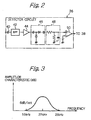
- Figure 2 shows a circuit diagram of the detector circuit 36.
- the detector circuit 36 includes a capacitor 40, a band pass filter 42, an amplifier 44, a rectifier circuit 46, a low pass filter 48, and a comparator 50.
- the band switching pulse signal having the frequency of 22 ⁇ 4 kHz is superimposed on the power supply voltage signal (13 volts or 18 volts) in the BS tuner 14 by tuning the television set to a channel to receive a BS signal included in the high frequency band of 11.7 GHz to 12.75 GHz
- the band switching pulse signal is input together with the intermediate frequency signals BS-IF to the band pass filter 42 through the capacitor 40, but only the band switching pulse signal is allowed to pass through the band pass filter 42.
- the band switching pulse signal is input to the amplifier 44 so as to be amplified to a given voltage level.
- the amplified band switching pulse signal is rectified by the rectifier circuit 46, and then an amplitude of the rectified band switching pulse signal is detected by the low pass filter 48.
- both the rectifier circuit 46 and the low pass filter 48 function as an amplitude detector for detecting the amplitude of the band switching pulse signal, so that the detected amplitude is output as an amplitude voltage signal from the low pass filter 48 to the comparator 50.
- the amplitude voltage signal is compared with a predetermined reference voltage.
- the amplitude voltage signal, derived from the band switching pulse signal, is higher than the reference voltage of the comparator 50, so that a high level signal is output from the comparator 50 to the selector circuit 38.
- the drive control signal, output from the selector circuit 38 to the second local oscillator 32H is changed from the low level to the high level
- the drive control signal, output from the selector circuit 38 to the first local oscillator 32L is changed from the high level to the low level.
- the second local oscillator 32H is driven so that the conversion of the BS signals, included in the high frequency band of 11.7 GHz to 12.75 GHz, into the intermediate frequency signals BS-IF is carried out.
- the band switching pulse signal having the frequency of 22 ⁇ 4 kHz is not superimposed on the power supply voltage signal (13 volts or 18 volts), i.e. when the television set is tuned to a channel to receive a BS signal included in the low frequency band of 10.7 GHz to 11.7 GHz, the amplitude voltage signal, output from the low pass filter 48, is lower than the reference voltage of the comparator 50, so that a low level signal is output from the comparator 50 to the selector circuit 38.
- the drive control signal, output from the selector circuit 38 to the first local oscillator 32L, is changed from the low level to the high level
- the drive control signal, output from the selector circuit 38 to the second local oscillator 32H is changed from the high level to the low level.
- the first local oscillator 32L is driven so that the conversion of the BS signals, included in the low frequency band of 10.7 GHz to 11.7 GHz, into the intermediate frequency signals BS-IF is carried out.
- the band pass filter 42 may have a frequency/amplitude characteristic as shown in a graph of Fig. 3.
- each of the side bands of the amplitude characteristic features a gradual slope, and thus the detector circuit 36 is susceptible to a noise having a large amplitude, such as a spike noise or the like, which is generated when the power supply voltage signal is switched between the low voltage (e.g. 13 volts) and the high voltage (e.g. 18 volts) or which is generated from internal combustion engines of motorcycles or automobiles.
- a malfunction of the detector circuit 36 may occur. Namely, the control circuit 22 may mistakenly select which local oscillator 32L or 32H should be driven.
- a sensitivity of the detector circuit 36 for detecting the band switching pulse signal (22 ⁇ 4 kHz) is inferior.
- the low pass filter is also susceptible to a noise having a large amplitude, such a spike noise or the like.
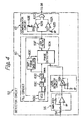
- a detector circuit generally indicated by reference 52, is substituted for the detector circuit 36.
- the detector circuit 52 includes a capacitor 54, an amplifier 56, a level detector circuit 58, a phase-locked loop (PLL) circuit 60, and a comparator circuit 62.
- PLL phase-locked loop
- the band switching pulse signal having the frequency of 22 ⁇ 4 kHz is super imposed on the power supply voltage signal (13 volts or 18 volts) in the BS tuner 14 by tuning the television set to a channel to receive a BS signal included in the high frequency band of 11.7 GHz to 12.75 GHz
- the band switching pulse signal is input together with the intermediate frequency signals BS-IF to the amplifier 56 through the capacitor 54.
- the band switching pulse signal is input to the amplifier 44 so as to be amplified to a given voltage level, and the amplified band switching pulse signal is input to the level detector 58.
- both the capacitor 54 and the amplifier 56 form a high pass filter.
- the level detector circuit 58 has a comparator 58A featuring a hysteresis characteristic, and the amplified band switching pulse signal is compared with a predetermined threshold voltage by the comparator 58A.
- the predetermined threshold voltage is lower than a peak voltage of the amplified band switching pulse signal, and thus a pulse signal, having substantially the same frequency as that (22 ⁇ 4 kHz) of the band switching pulse signal, is output from the level detector circuit 58 to the PLL circuit 60.
- the pulse signal output from the level detector circuit 58 may be referred to as a band switching pulse signal, this band switching pulse signal is free from the various noises involved in the original band switching pulse signal, due to the hysteresis characteristic of the comparator 58A.
- the band switching pulse signal is wave-shaped by the comparator 58A, and the wave-shaped band switching pulse signal is input to the PLL circuit 60.
- the PLL circuit 60 has a phase detector 60A, a voltage control oscillator (VCO) 60B, a first frequency divider 60C, a second frequency divider 60D, a 180°-phase shifter 60E, and a loop filter (low pass filter).
- VCO voltage control oscillator
- the band switching pulse signal output from the level detector circuit 58 is input to the phase detector 60A of the PLL circuit 60.
- the VCO 60B is of a free-running oscillation type, and outputs a first oscillation signal having a frequency, which is near to 88 kHz, to the first frequency divider 60C, in which the first oscillation signal (88 kHz) is converted into a second oscillation signal having a frequency which is near to 44 kHz. Then, the second oscillation signal (44 kHz) is input from the first frequency divider 60C to the second frequency divider 60D, in which the second oscillation signal (44 kHz) is further converted into a third oscillation signal having a frequency which is near to 22 kHz, and the third oscillation signal (22 kHz) is input from the second frequency divider 60D to the phase detector 60A.
- the third oscillation signal (22 kHz) is input from the second frequency divider 60D to the 180° -phase shifter 60E, in which the phase of the input third oscillation signal (22 kHz) is shifted by 180° with respect to the phase of the original oscillation signal (22 kHz) output from the second frequency divider 60D, to thereby produce a 180°-phase-shifted oscillation signal.
- the produced 180°-phase-shifted pulse signal (22 kHz) is input from the 180°-phase shifter 60E to the phase detector 60A.
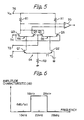
- the phase detector 60A may be constituted as a double-balanced-multiplier, which includes a first differential amplifier 64 having two transistors Q1 and Q2 forming a differential pair, a second differential amplifier 66 having two transistors Q3 and Q4 forming a differential pair, a third differential amplifier 68 having two transistors Q5 and Q6 forming a differential pair, and a comparator 70.
- the transistors Q1 to Q6 and the comparator CMP are arranged and connected to each other, as shown in Fig. 5.
- Both the bases of the transistors Q4 and Q5 are connected to an input terminal 74 for inputting the third oscillation signal (22 kHz) from the second frequency divider 60D.
- Both the bases of the transistors Q3 and Q6 are connected to an input terminal 76 for inputting the 180°-phase-shifted pulse signal (22 kHz) from the 180°-phase shifter 60E.
- the respective 180°-phase-shifted pulse signal (22 kHz) and third oscillation signal (22 kHz) may be input to the input terminals 72 and 74.
- reference 76 indicates an input terminal for inputting a power supply voltage V CC from the power source circuit 18 (Fig. 1), and the power supply voltage V CC is applied to the collectors of the transistors Q3 and Q6 through respective resistors R1 and R2.
- the emitters of the transistor Q1 and Q2 are grounded through a resistor R3.
- the base of the transistor Q2 is connected to a voltage source 71.
- the output terminal of the comparator 70 is connected to the loop filter 60F (Fig. 4).
- the PLL circuit 60 is locked to thereby establish a locked state, in which the phase of the band switching pulse signal is advanced or retarded by 90° with respect to the phase of the third oscillation signal (22 kHz) output from the second frequency divider 60D so that a voltage of approximately V CC /2 is output from the loop filter 60F.
- the comparator circuit 62 is constituted as a window-type comparator circuit.
- the window-type comparator includes a first comparator 62A having a reference voltage of 1 volt, a second comparator 62B having a reference voltage of 3 volts, and an AND-gate 62C.
- the respective reference voltages of 1 volt and 3 volts are obtained from variable voltage sources 62D and 62E.
- both the first and second comparators 62A and 62B output respective high level signals to the AND-gate 62C, and thus a high level signal is output from the AND-gate 62C to the selector circuit 38 (Fig. 1).
- the second local oscillator 32H is driven so that the conversion of the BS signals, included in the high frequency band of 11.7 GHz to 12.75 GHz, into the intermediate frequency signals BS-IF is carried out.
- the drive control signal, output from the selector circuit 38 to the first local oscillator 32L, is changed from the low level to the high level
- the drive control signal, output from the selector circuit 38 to the second local oscillator 32H is changed from the high level to the low level.
- the first local oscillator 32L is driven so that the conversion of the BS signals, included in the low frequency band of 10.7 GHz to 11.7 GHz, into the intermediate frequency signals BS-IF is carried out.
- the PLL circuit 60 may have a frequency/amplitude characteristic as shown in a graph of Fig. 6. As shown in this graph, the frequency/amplitude characteristic features a rectangular profile, the sides of which are defined by the frequencies of 18 kHz and 26 kHz, and thus the detector circuit 52 is not susceptible to various noises, resulting in a satisfactory reliable operation of the BS converter according to the present invention.
- the band switching pulse signal (22 ⁇ 4 kHz) is superimposed on the power supply voltage signal (13 volts or 18 volts), it is possible to ensure the establishment of the locked state in the PLL circuit 60, and thus a sensitivity of the detector circuit 52 for detecting the band switching pulse signal (22 ⁇ 4 kHz) is superior to the case of the above-mentioned prior art BS converter.
- the band switching pulse signal (22 ⁇ 4 kHz) is superimposed on the power supply voltage signal (13 volts or 18 volts)
- the frequency of the band switching pulse signal is sufficiently lower than that (950 to 2150 MHz) of the intermediate frequency signal BS-IF.
Landscapes
- Physics & Mathematics (AREA)
- Astronomy & Astrophysics (AREA)
- General Physics & Mathematics (AREA)
- Engineering & Computer Science (AREA)
- Signal Processing (AREA)
- Input Circuits Of Receivers And Coupling Of Receivers And Audio Equipment (AREA)
- Superheterodyne Receivers (AREA)
- Two-Way Televisions, Distribution Of Moving Picture Or The Like (AREA)
Applications Claiming Priority (2)
| Application Number | Priority Date | Filing Date | Title |
|---|---|---|---|
| JP2004020118A JP3898187B2 (ja) | 2004-01-28 | 2004-01-28 | 衛星放送用コンバータのスイッチ回路 |
| JP2004020118 | 2004-01-28 |
Publications (2)
| Publication Number | Publication Date |
|---|---|
| EP1560353A2 true EP1560353A2 (de) | 2005-08-03 |
| EP1560353A3 EP1560353A3 (de) | 2011-08-03 |
Family
ID=34650797
Family Applications (1)
| Application Number | Title | Priority Date | Filing Date |
|---|---|---|---|
| EP05001714A Withdrawn EP1560353A3 (de) | 2004-01-28 | 2005-01-27 | Konverter für Satellitenrundfunk, und darin verwendete Detektorschaltung |
Country Status (5)
| Country | Link |
|---|---|
| US (1) | US20050164629A1 (de) |
| EP (1) | EP1560353A3 (de) |
| JP (1) | JP3898187B2 (de) |
| CN (1) | CN100418306C (de) |
| TW (1) | TWI260129B (de) |
Cited By (1)
| Publication number | Priority date | Publication date | Assignee | Title |
|---|---|---|---|---|
| CN107820121A (zh) * | 2017-11-06 | 2018-03-20 | 深圳创维-Rgb电子有限公司 | C波段卫星数字广播频道的搜索方法、电视及存储装置 |
Families Citing this family (8)
| Publication number | Priority date | Publication date | Assignee | Title |
|---|---|---|---|---|
| JP3863538B2 (ja) * | 2004-06-01 | 2006-12-27 | Necエレクトロニクス株式会社 | 衛星放送用コンバータのスイッチ回路 |
| JP4934529B2 (ja) * | 2007-07-09 | 2012-05-16 | 株式会社日立製作所 | 無線受信回路、並びに無線トランシーバ回路及びそのキャリブレーション方法 |
| CN101895707A (zh) * | 2010-06-29 | 2010-11-24 | 苏州市华芯微电子有限公司 | 可集成的22KHz包络检测及频带开关电路 |
| CN101945230A (zh) * | 2010-08-12 | 2011-01-12 | 无锡市晶源微电子有限公司 | 卫星电视信号C、Ku波段射频放大电路的单片控制电路 |
| CN102523400A (zh) * | 2011-12-23 | 2012-06-27 | 苏州华芯微电子股份有限公司 | 一种卫星接收控制集成电路 |
| TWI498572B (zh) * | 2013-05-07 | 2015-09-01 | Wistron Corp | 自動測量dvb-s接收裝置的調諧器的輸出電壓的方法、轉接器及dvb-s接收裝置 |
| CN106412647B (zh) * | 2015-07-29 | 2019-05-31 | 国基电子(上海)有限公司 | 信号切换系统及应用该信号切换系统的机顶盒 |
| JP7155042B2 (ja) * | 2019-02-22 | 2022-10-18 | ホシデン株式会社 | センサ制御装置 |
Citations (4)
| Publication number | Priority date | Publication date | Assignee | Title |
|---|---|---|---|---|
| US3893042A (en) * | 1973-12-12 | 1975-07-01 | Us Navy | Lock indicator for phase-locked loops |
| US3952261A (en) * | 1972-11-06 | 1976-04-20 | Fujitsu Ltd. | Signal detection circuit |
| EP0319415A1 (de) * | 1987-12-03 | 1989-06-07 | Institut Français du Pétrole | Einrichtung zum schnellen, bei schwachem Rauschen, Regeln der Frequenz und Phase eines Signals auf ein aufgezwungenes Signal |
| US6081224A (en) * | 1995-02-13 | 2000-06-27 | Parker Hannifin Corporation | High accuracy, low speed doppler effect radar and signal conditioning circuit useful in agricultural applications |
Family Cites Families (10)
| Publication number | Priority date | Publication date | Assignee | Title |
|---|---|---|---|---|
| US4476580A (en) * | 1980-06-17 | 1984-10-09 | Sanyo Electric Co., Ltd. | Automatic continuous tuning control apparatus for a receiver |
| JP3345114B2 (ja) * | 1992-08-18 | 2002-11-18 | コーニンクレッカ フィリップス エレクトロニクス エヌ ヴィ | 高周波信号受信機 |
| CN2167485Y (zh) * | 1993-08-05 | 1994-06-01 | 全泽松 | 单片红外无线耳机 |
| JP2988844B2 (ja) * | 1995-04-25 | 1999-12-13 | シャープ株式会社 | 衛星放送用コンバータのスイッチング回路 |
| US5654774A (en) * | 1995-06-06 | 1997-08-05 | Thomson Consumer Electronics, Inc. | Tuner for digital satellite receiver |
| JP2842327B2 (ja) * | 1995-08-16 | 1999-01-06 | 日本電気株式会社 | 広帯域逓倍器 |
| JP3250796B2 (ja) * | 1998-05-26 | 2002-01-28 | 松下電器産業株式会社 | 受信機 |
| GB0030965D0 (en) * | 2000-12-19 | 2001-01-31 | Nokia Oy Ab | Improvements relating to satellite reception` |
| US6529000B2 (en) * | 2000-12-29 | 2003-03-04 | Ge Medical Systems Global Technology Company, Llc | Method and system for processing magnetic resonance signals to remove transient spike noise |
| US7149270B2 (en) * | 2001-05-03 | 2006-12-12 | Coreoptics, Inc. | Clock recovery circuit |
-
2004
- 2004-01-28 JP JP2004020118A patent/JP3898187B2/ja not_active Expired - Fee Related
-
2005
- 2005-01-27 TW TW094102470A patent/TWI260129B/zh not_active IP Right Cessation
- 2005-01-27 EP EP05001714A patent/EP1560353A3/de not_active Withdrawn
- 2005-01-27 US US11/043,152 patent/US20050164629A1/en not_active Abandoned
- 2005-01-28 CN CNB2005100061311A patent/CN100418306C/zh not_active Expired - Fee Related
Patent Citations (4)
| Publication number | Priority date | Publication date | Assignee | Title |
|---|---|---|---|---|
| US3952261A (en) * | 1972-11-06 | 1976-04-20 | Fujitsu Ltd. | Signal detection circuit |
| US3893042A (en) * | 1973-12-12 | 1975-07-01 | Us Navy | Lock indicator for phase-locked loops |
| EP0319415A1 (de) * | 1987-12-03 | 1989-06-07 | Institut Français du Pétrole | Einrichtung zum schnellen, bei schwachem Rauschen, Regeln der Frequenz und Phase eines Signals auf ein aufgezwungenes Signal |
| US6081224A (en) * | 1995-02-13 | 2000-06-27 | Parker Hannifin Corporation | High accuracy, low speed doppler effect radar and signal conditioning circuit useful in agricultural applications |
Cited By (1)
| Publication number | Priority date | Publication date | Assignee | Title |
|---|---|---|---|---|
| CN107820121A (zh) * | 2017-11-06 | 2018-03-20 | 深圳创维-Rgb电子有限公司 | C波段卫星数字广播频道的搜索方法、电视及存储装置 |
Also Published As
| Publication number | Publication date |
|---|---|
| JP3898187B2 (ja) | 2007-03-28 |
| CN1671059A (zh) | 2005-09-21 |
| TWI260129B (en) | 2006-08-11 |
| EP1560353A3 (de) | 2011-08-03 |
| JP2005217635A (ja) | 2005-08-11 |
| CN100418306C (zh) | 2008-09-10 |
| US20050164629A1 (en) | 2005-07-28 |
| TW200534611A (en) | 2005-10-16 |
Similar Documents
| Publication | Publication Date | Title |
|---|---|---|
| CA1224529A (en) | Shf receiver | |
| US6094236A (en) | Tuner circuit | |
| EP1560353A2 (de) | Konverter für Satellitenrundfunk, und darin verwendete Detektorschaltung | |
| US4422096A (en) | Television frequency synthesizer for nonstandard frequency carriers | |
| US3611152A (en) | Stabilized automatic tuning receiver | |
| CA2020387C (en) | Station selecting apparatus | |
| US6211925B1 (en) | Video intermediate-frequency signal processing device capable of receiving FM broadcasts | |
| US4320530A (en) | Channel selecting apparatus employing frequency synthesizer | |
| US5995169A (en) | SIF signal processing circuit | |
| EP0668656B1 (de) | Tuner für Satelliten-Rundfunkempfänger | |
| JP3725402B2 (ja) | テレビジョンチューナ | |
| US7426368B2 (en) | Satellite broadcasting converter, control circuit incorporated therein, and detector circuit used in such control circuit | |
| US6353462B1 (en) | Television signal and FM broadcast signal demodulator and television signal and FM broadcast signal receiver | |
| US20020030763A1 (en) | Receiver | |
| US7245872B2 (en) | Satellite broadcasting converter, control circuit incorporated therein, and detector circuit used in such control circuit | |
| US20070146550A1 (en) | Receiving circuit, receiving apparatus, and receiving method | |
| JP4468633B2 (ja) | 周波数変換装置 | |
| KR970007889B1 (ko) | 위성방송 및 케이블방송 겸용 튜너 | |
| KR0133724Y1 (ko) | 오디오 변환회로 | |
| KR890002594B1 (ko) | 위성방송과 tv방송 입체형 수신기의 튜닝회로 | |
| US4547805A (en) | Television AFC system usable with offset carrier frequencies | |
| KR100435402B1 (ko) | 동일방송국을비교하여자동선국하는라디오장치 | |
| KR940002572Y1 (ko) | Aft를 이용한 비디오신호 억제 회로 | |
| JP2005348234A (ja) | テレビジョンチューナ | |
| JPS627729B2 (de) |
Legal Events
| Date | Code | Title | Description |
|---|---|---|---|
| PUAI | Public reference made under article 153(3) epc to a published international application that has entered the european phase |
Free format text: ORIGINAL CODE: 0009012 |
|
| AK | Designated contracting states |
Kind code of ref document: A2 Designated state(s): AT BE BG CH CY CZ DE DK EE ES FI FR GB GR HU IE IS IT LI LT LU MC NL PL PT RO SE SI SK TR |
|
| AX | Request for extension of the european patent |
Extension state: AL BA HR LV MK YU |
|
| RAP1 | Party data changed (applicant data changed or rights of an application transferred) |
Owner name: RENESAS ELECTRONICS CORPORATION |
|
| PUAL | Search report despatched |
Free format text: ORIGINAL CODE: 0009013 |
|
| AK | Designated contracting states |
Kind code of ref document: A3 Designated state(s): AT BE BG CH CY CZ DE DK EE ES FI FR GB GR HU IE IS IT LI LT LU MC NL PL PT RO SE SI SK TR |
|
| AX | Request for extension of the european patent |
Extension state: AL BA HR LV MK YU |
|
| 17P | Request for examination filed |
Effective date: 20120201 |
|
| AKX | Designation fees paid |
Designated state(s): DE GB |
|
| 17Q | First examination report despatched |
Effective date: 20120510 |
|
| STAA | Information on the status of an ep patent application or granted ep patent |
Free format text: STATUS: THE APPLICATION HAS BEEN WITHDRAWN |
|
| 18W | Application withdrawn |
Effective date: 20141024 |
|
| REG | Reference to a national code |
Ref country code: DE Ref legal event code: R079 Free format text: PREVIOUS MAIN CLASS: H04H0001000000 Ipc: H04H0020000000 |
|
| REG | Reference to a national code |
Ref country code: DE Ref legal event code: R079 Free format text: PREVIOUS MAIN CLASS: H04H0001000000 Ipc: H04H0020000000 Effective date: 20141203 |