EP1560262B1 - Plasma etching chamber and plasma etching system using same - Google Patents
Plasma etching chamber and plasma etching system using same Download PDFInfo
- Publication number
- EP1560262B1 EP1560262B1 EP03774252.5A EP03774252A EP1560262B1 EP 1560262 B1 EP1560262 B1 EP 1560262B1 EP 03774252 A EP03774252 A EP 03774252A EP 1560262 B1 EP1560262 B1 EP 1560262B1
- Authority
- EP
- European Patent Office
- Prior art keywords
- wafer
- wafers
- plasma etching
- periphery
- plasma
- Prior art date
- Legal status (The legal status is an assumption and is not a legal conclusion. Google has not performed a legal analysis and makes no representation as to the accuracy of the status listed.)
- Expired - Lifetime
Links
Images


Classifications
-
- H—ELECTRICITY
- H10—SEMICONDUCTOR DEVICES; ELECTRIC SOLID-STATE DEVICES NOT OTHERWISE PROVIDED FOR
- H10P—GENERIC PROCESSES OR APPARATUS FOR THE MANUFACTURE OR TREATMENT OF DEVICES COVERED BY CLASS H10
- H10P50/00—Etching of wafers, substrates or parts of devices
- H10P50/20—Dry etching; Plasma etching; Reactive-ion etching
- H10P50/24—Dry etching; Plasma etching; Reactive-ion etching of semiconductor materials
- H10P50/242—Dry etching; Plasma etching; Reactive-ion etching of semiconductor materials of Group IV materials
-
- H—ELECTRICITY
- H10—SEMICONDUCTOR DEVICES; ELECTRIC SOLID-STATE DEVICES NOT OTHERWISE PROVIDED FOR
- H10P—GENERIC PROCESSES OR APPARATUS FOR THE MANUFACTURE OR TREATMENT OF DEVICES COVERED BY CLASS H10
- H10P70/00—Cleaning of wafers, substrates or parts of devices
- H10P70/50—Cleaning of wafers, substrates or parts of devices characterised by the part to be cleaned
-
- H—ELECTRICITY
- H01—ELECTRIC ELEMENTS
- H01J—ELECTRIC DISCHARGE TUBES OR DISCHARGE LAMPS
- H01J37/00—Discharge tubes with provision for introducing objects or material to be exposed to the discharge, e.g. for the purpose of examination or processing thereof
- H01J37/32—Gas-filled discharge tubes
- H01J37/32009—Arrangements for generation of plasma specially adapted for examination or treatment of objects, e.g. plasma sources
- H01J37/32082—Radio frequency generated discharge
- H01J37/32091—Radio frequency generated discharge the radio frequency energy being capacitively coupled to the plasma
-
- H—ELECTRICITY
- H01—ELECTRIC ELEMENTS
- H01J—ELECTRIC DISCHARGE TUBES OR DISCHARGE LAMPS
- H01J37/00—Discharge tubes with provision for introducing objects or material to be exposed to the discharge, e.g. for the purpose of examination or processing thereof
- H01J37/32—Gas-filled discharge tubes
- H01J37/32431—Constructional details of the reactor
- H01J37/32532—Electrodes
-
- H—ELECTRICITY
- H01—ELECTRIC ELEMENTS
- H01J—ELECTRIC DISCHARGE TUBES OR DISCHARGE LAMPS
- H01J2237/00—Discharge tubes exposing object to beam, e.g. for analysis treatment, etching, imaging
- H01J2237/32—Processing objects by plasma generation
- H01J2237/33—Processing objects by plasma generation characterised by the type of processing
- H01J2237/334—Etching
Definitions
- the present invention relates to a system of removing a film material and particles left at the periphery of a semiconductor wafer, and in particular, to a plasma etching chamber capable of completely removing a film material and particles left and deposited at the periphery of the dry etched wafer during plasma etching, and a plasma etching system using the same.
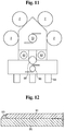
- thin film process and dry etching process are very important but the film material is unnecessarily deposited at the periphery of the wafer during the thin film process, and in addition, with the dry cleaning of the top surface of the wafer through plasma etching, the by-product generated during the plasma etching is not completely exhausted, but deposited throughout the top, the lateral and the bottom sides of the periphery of the wafer as particles.
- particles 93 are deposited at the peripheral end of the wafer 91 continuously from the top thereof to the bottom through the lateral side, and intruded to the gap between the wafer 91 and a stage 95.
- the periphery of the wafer is not used to form a semiconductor chip, but the film material and the particles left thereat (referred to hereinafter as the "particles") cause serious damages to the semiconductor chips during the subsequent semiconductor processing steps.
- the particles deposited at the peripheral end of the wafer may be removed through wet cleaning, but the wet cleaning is liable to induce other device failures with the cleaned semiconductor.
- the remnant solution remained after the cleaning has a high reactivity as an environmentally bad polluting material, and hence, it is difficult to waste-dispose the solution.
- Japanese Patent Laid-open Publication No. Hei07-142449 discloses a device for plasma etching to remove the particles left at the peripheral end of the wafer.
- a reaction gas is blown to the space between top and bottom electrodes arranged corresponding to the periphery of the wafer to make the plasma etching, and an inert gas is blown to the center of the top electrode to prevent the generated plasma from being intruded to the wafer.
- the above device has a structure of applying radio frequency to the top electrode facing the wafer while not applying the self bias to the wafer, it involves slow etching speed and long processing time.
- the etching is performed only with respect to the top surface of the periphery of the wafer so that the particles deposited throughout the lateral to the bottom sides thereof cannot be completely removed.
- KR 2002 0080955 discloses a plasma etching apparatus to reduce a fabricating cost of a semiconductor device and improve a yield of the semiconductor device by removing particles accumulated on an edge of a wafer.
- EP 0 714 998 discloses a CVD processing chamber wherein a choke region of flow through each opening in an inner chamber surface communicates with a vacuum duct in a wall of the chamber and is generally equally distributed from said central axis of said substrate.
- the plasma etching chamber includes a cathode for applying radio frequency to a wafer through a built-in stage, a ring-shaped bottom anode placed at the outer circumference of the stage while being positioned below the periphery of the wafer, and a ring-shaped top anode placed over the stage while facing the ring-shaped bottom anode.
- the discharge is created between the peripheral end of the wafer and the ring-shaped top anode as well as between the peripheral end of the wafer and the ring-shaped bottom anode while generating plasma to continuously etch the top to the bottom sides of the periphery of the wafer.
- a plasma etching system as defined in claim 7 or 8.
- the plasma etching chamber also includes a groove formed at the periphery of the insulator to make a point of inflection in the flow of the reaction gas.
- the etching chamber includes a stage mounted with a wafer, a ring-shaped top anode and a ring-shaped bottom cathode placed around the periphery of the wafer while facing each other and a view-ring placed at the outer circumference of the ring-shaped top anode while limiting the plasma space.
- the pressure distribution of the reaction gas flown between the ring-shaped top anode and the ring-shaped bottom cathode is controlled such that the plasma generated due to the discharge effectively etches the top to the bottom sides of the periphery of the wafer.
- the groove may be formed at a disk-shaped insulator placed over the stage and facing it while extending parallel to the wafer to form the etching boundary with a vertical shape.
- the center of the insulator placed over the wafer while facing it may be formed with a concave surface to inhibit the discharge there around.
- the plasma etching chamber according to the present invention may further include means for stably mounting the wafer onto the stage, or laser sensor for measuring the discharge distance between the top surface of the wafer and the ring-shaped top anode and controlling it to be at an optimum value, thereby conducting the wafer etching optimally.
- the plasma etching chamber according to the present invention may further include an aligner for correcting the posture of the wafer mounted on the stage.
- a handler when wafer-loaded cassettes are fed to any one of plural numbers of cassette stands, a handler takes the wafers from the stands, and brings them to a wafer alignment unit. When the wafers are posture-corrected at the orientation flat (OF) locations thereof, the handler takes the wafers from the wafer alignment unit, and moves them into plasma etching chambers. When the etching of the wafers is completed, the handler takes the wafers from the chambers, and loads them to the initial cassettes.
- OF orientation flat
- a subsidiary handler takes the wafers from the load ports, and brings them to a wafer alignment unit to posture-correct the OF locations thereof.
- a handler takes the wafers from the load lock chambers, and moves them into any one of plural numbers of etching chambers.
- the handler takes the wafers from the chambers, and moves them into load lock chambers.
- the subsidiary handler takes the wafers from the load lock chambers, and returns them to the initial cassettes.
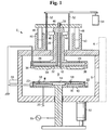
- Fig. 1 illustrates the structure of an etching chamber.
- the chamber 2 has an inner space 8 isolated from the outside by closing a door 4 of a gate 6 through which a wafer W goes in or out.
- a stage 10 is placed at the center of the inner space 8 to mount the wafer W thereon.
- the atmosphere thereof is controlled to be under the low pressure of about 10 -1 -10 -3 Torr.
- a cathode 14 is placed at the center of the top surface of the stage 10 such that it can be elevated by an actuator 12, and connected to a plasma oscillator 16.
- a water jacket 18 is provided within the stage 10 to forcefully cool it such that a coolant can be circulated via at least two paths 20 communicated with the outside.
- a ring-shaped bottom anode 22 is attached to the outer circumference of the stage 10 by interposing an insulating material 23.
- the cathode 14 receives the wafer W from the top, and descends to a predetermined location to mount it on the stage 10.
- the ring-shaped bottom anode 22 should be positioned lower than the wafer W such that a predetermined distance is made between the anode 22 and the periphery of the wafer W mounted on the stage 10 to allow the discharge.
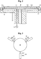
- the stage 10 has the structure shown in Fig. 2 .
- an insulating plate 100 with a cathode 14 is placed on the stage 10, and a plate 104 with at least three pins 102 is placed under the insulating plate 104.
- the pin 102 penetrates through the insulating plate 100 while being protruded to the top.
- the plate 104 is connected to an actuator 12 such that it can be elevated.
- the cathode 14 is located at the center of the bottom surface of the insulating plate 100.
- the bottom surface of the wafer W is supported by the pins 102 protruded over the stage 10, and when the actuator 12 descends, the wafer W is mounted onto the insulating plate 100 without shaking.
- a stem 24 is placed over the stage 10 with almost the same area such that it can move up and down by way of a rod 26 extended upward. Furthermore, as like with the stage 10, a water jacket 28 is provided within the stem 24 such that a coolant is circulated via a path 30 communicated with the inner space of the rod 26.
- An insulator 34 is attached to the bottom surface of the stem 24, and has a concave surface 32 with a predetermined radius at the center thereof.
- a ring-shaped top anode 36 is mounted around the insulator 34 while facing the bottom anode 22. The top and the bottom anodes 36 and 22 are all earthed to the ground.
- the discharge is liable to be made over the entire area thereof while generating plasma at the center of the wafer W, thereby making unnecessary etching.
- the center of the insulator 34 is spaced apart from the top surface of the wafer W with a larger distance due to the presence of the concave portion 32, the strength of the electric field at that area becomes weak, and the discharge is not made at the concave portion 32.
- the relation between the thickness of the insulator 34 and the discharge should not be disregarded. It was confirmed through experiments that when the thickness of the insulator 34 is less than 15mm and the discharge is stably made at the periphery thereof, the discharge was also made at the center thereof even with the presence of the concave portion 32.
- the thickness of the insulator 34 is preferably established to be 15mm or more.
- a ring-shaped reaction gas outlet 38 is placed between the insulator 34 and the top anode 36, and opens to blow the reaction gas injected through a first tube passage 40 to the periphery of the wafer W.
- a nitrogen gas outlet 42 is placed at the central concave portion 32 of the insulator 34, and opens to blow the nitrogen gas fed through a second tube passage 44 to the center of the wafer W.
- the rod 26 with the first and the second tube passages 40 and 44 is connected to post bars 48 at its outer ends by mediating a horizontal bar 46, and the post bars 48 are axially supported by guiders 50 provided at the outer top surface of the chamber 2 such that they move up and down without shaking.
- the elevation of the rod 26 is made by ball screws 52 and a stepping motor 54 in synchronization with the horizontal bar 46.
- a laser sensor 56 is provided at the outer circumference of the chamber 2 to measure the gap between the wafer W and the top anode 36 and feedback the measurement result to a controller, thereby controlling the descending location of the stem 24 correctly.
- a plurality of radial direction-controlling aligners 58 is equidistantly arranged around the top surface of the stage 10 in the space 8.
- the aligners 58 are formed each with a piston rod 582 moving forward and backward by way of a cylinder 580.
- the piston rods 582 are elongated all with the same length while slightly holding or pressing the periphery of the wafer W to align the center thereof. In this way, the wafer W is corrected to its proper posture, and finally, the orientation flat (OF) locations thereof agree to each other.
- the plasma may be generated only at those portions.
- the nitrogen gas blown through the nitrogen gas outlet 42 makes formation of an air curtain at the center of the wafer W, and prevents the reaction radicals generated at the periphery of the wafer W during the etching from flowing to the center thereof.
- the plasma is generated only at the periphery thereof.
- the thickness of the space charge sheath S may be minimized by controlling the vacuum degree of the chamber 2 and the radio frequency oscillating degree in such a way as to not hinder the plasma etching, but the influence thereof cannot be completely removed.
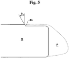
- Fig. 5 illustrates the result of etching the periphery of a wafer W using the etching chamber according to the embodiment of the present invention.
- the etching boundary at the peripheral end of the wafer W is formed with an inclined side Ws with an etching angle ⁇ due to the influence of the space charge sheath S.
- the etched area and the particles P deposited at the end thereof are indicated by the dotted line.
- the etching angle ⁇ reaches 2-3°, at which the wafer device is not damaged.
- a groove 64 is formed at the outer circumference of the insulator 34 parallel to the wafer W.
- the reaction gas ridden along the outer circumference thereof meets the inner circumference of the groove 64, and is inflected along the groove 64 so that the plasma is diffused while generating neutral F radicals R.
- the neutral F radicals R transmit the lower-sided space charge sheath S, and collide against the wafer W perpendicular to the surface thereof. Consequently, as shown in Fig. 7 , an optimum etching shape is made such that the etching boundary is nearly vertical to the periphery of the wafer W while being positioned slightly internal to the end thereof.
- the above-described structure according to the embodiment of the present invention includes the components of a cathode 14 and a pair of anodes 22 and 36, but the present invention is not limited thereto.
- Fig. 8 illustrates an etching chamber according to another embodiment of the present invention where the same components as those with the etching chamber according to the previous embodiment are indicated by like reference numerals.
- a ring-shaped bottom cathode 66 is attached to the outer circumference of a stage 10 instead of the ring-shaped bottom anode 22, and connected to a plasma oscillator 16.
- a view-ring 68 is attached external to a top anode 36 to inhibit the diffusion of the reaction gas.
- the view-ring 68 mechanically shields the ring-shaped anode 36 and the bottom cathode 66 such that the reaction gas is converged without diffusing to the outside, and flown via the bottom surface of the periphery of the wafer W. In this way, the plasma Ps is sufficiently generated throughout the top to the bottom sides of the wafer W.
- the flow pressure of the reaction gas can be controlled by properly establishing the distance G between the inner circumference of the viewing 68 and the outer circumference of the ring-shaped cathode 66.
- the plasma can be generated even with a lower power by limiting the plasma-generated region.
- a groove 64 may be formed at the outer circumference of the insulator 34 for the same purpose as with the previous embodiment.
- the groove 64 is formed at the outer circumference of the insulator 34 with the omission of the view-ring 68, thereby achieving the desired etching function.
- the reaction gas flown through the reaction gas outlet 38 is diffused while making a weak flow so that the etching for the peripheral end of the wafer W may be insufficient.
- the optimum etching region based on the point of inflection of the space charge sheath S induced by the groove 64 agrees to the peripheral end of the wafer W to thereby etch the peripheral end of the wafer W in a desired manner.
- the plasma-induced heat may be highly generated during the dry cleaning process, but the stage 10 and the stem 24 have a cooling structure to dissipate such a heat.
- de-ionized water ultra pure water
- An etching system with the structure shown in Fig. 10 may be realized using the etching chamber according to the embodiment of the present invention.
- the etching system includes a plurality of chambers 2, and a handler 70 placed front to the chambers 2.
- a plurality of cassette stands 72 and a wafer alignment unit 74 are placed around the handler 70. Wafers W are mounted at a cassette C, and delivered to any one of the cassette stands 72.
- the cassette stand 72 is preferably rotated at a predetermined angle with a driving member controlled by a sensor (not shown) such that the handler 70 takes the wafers W from the cassette C with balanced posture.
- a non-safety area is established around the cassette stands 72, and a body sensor 76 is provided there.
- the body sensor 76 senses it, and stops the operation of the handler 70.
- the handler 70 takes wafers W from the cassette C, and brings them to the wafer alignment unit 74.
- the wafer alignment unit 74 is rotated at a predetermined angle by the driving member, and aligns the wafers W to the inlets of the chambers 2, that is, the OF locations.
- the wafers W aligned by the wafer alignment unit 74 are taken by the handler 70, and charged into the chambers 2 through the gates 6 thereof, followed by mounting them onto the stages 10.
- the wafers W mounted on the stage 10 is finally aligned to the OF location by the aligner 58, and when the door 4 of the gate 6 closes, the inner space 8 of the chamber 2 is isolated from the outside while being kept to be in a vacuum state. Thereafter, the top-sided stem 24 descends such that it is located over the wafer W by a predetermined height.
- the descending of the stem 24 is measured by a laser sensor 56, and the distance between the stem 24 and the wafer W is controlled to be optimal for the etching.
- the operation of the stem 24 is stopped while issuing a warning or alarm signal.
- a nonvolatile gas and a reaction gas are fed to the wafer W from the outside so that the peripheral end of the wafer W is etched.
- the stem 24 ascends to return to the initial location, and the door 4 opens.
- the handler 70 recovers the etched wafer W, and loads it onto the cassette C. The recovered wafers W are delivered to the location for the subsequent process.
- the testing of the non-defective or the defective of the wafers W is conducted through the way of usual samplings.
- the reference numeral 78 of Fig. 10 indicates a refrigerator for supplying a coolant to the chamber 2 and circulating it
- the reference numeral 80 indicates a power matcher disposed between the chamber 2 and the plasma oscillator 16.
- the refrigerator 78 and the power matcher 80 are provided per each chamber 2. Alternatively, they may be common to all of the chambers 2 as a single unit.
- Fig. 11 illustrates an etching system according to another embodiment of the present invention.
- a plurality of chambers 2 are arranged around the handler 70, and a plurality of load lock chambers 82 are provided at the inlet and the outlet of the handler 70.
- a plurality of load ports 84 are continuously arranged close to the load lock chambers 82.
- the wafers W are delivered between the load lock chambers 82 and the load ports 84 by way of a subsidiary handler 86, and before they are charged into the load lock chambers 82, they are corrected in their postures by an aligner 88.
- the charging, taking out and the posture correction of the wafer W are conducted by the handler and the aligner as like with the previous embodiment, but a large number of chambers 2 may be arranged, and the dry cleaning of the wafer may be automatically conducted by the collective process of sequential controlling.
- the top, the lateral and the bottom sides of the periphery of the wafer are etched with a single process, or the peripheral end of the wafer is correctly etched.
- the target portion of the periphery of the wafer can be etched within a short period of time, and the processing efficiency per the unit time is heightened. This serves to reduce the production cost of the semiconductor device.
- the processing steps can be simplified.
Landscapes
- Physics & Mathematics (AREA)
- Engineering & Computer Science (AREA)
- Plasma & Fusion (AREA)
- Chemical & Material Sciences (AREA)
- Analytical Chemistry (AREA)
- Drying Of Semiconductors (AREA)
- Cleaning Or Drying Semiconductors (AREA)
Description
- The present invention relates to a system of removing a film material and particles left at the periphery of a semiconductor wafer, and in particular, to a plasma etching chamber capable of completely removing a film material and particles left and deposited at the periphery of the dry etched wafer during plasma etching, and a plasma etching system using the same.
- For the fabrication of an integrated circuit , thin film process and dry etching process are very important but the film material is unnecessarily deposited at the periphery of the wafer during the thin film process, and in addition, with the dry cleaning of the top surface of the wafer through plasma etching, the by-product generated during the plasma etching is not completely exhausted, but deposited throughout the top, the lateral and the bottom sides of the periphery of the wafer as particles.
- That is, with the plasma-etched wafer, as shown in
Fig. 12 ,particles 93 are deposited at the peripheral end of thewafer 91 continuously from the top thereof to the bottom through the lateral side, and intruded to the gap between thewafer 91 and astage 95. - The periphery of the wafer is not used to form a semiconductor chip, but the film material and the particles left thereat (referred to hereinafter as the "particles") cause serious damages to the semiconductor chips during the subsequent semiconductor processing steps.
- The particles deposited at the peripheral end of the wafer may be removed through wet cleaning, but the wet cleaning is liable to induce other device failures with the cleaned semiconductor. The remnant solution remained after the cleaning has a high reactivity as an environmentally bad polluting material, and hence, it is difficult to waste-dispose the solution.
- Japanese Patent Laid-open Publication No.
Hei07-142449 - With the disclosed etching device, a reaction gas is blown to the space between top and bottom electrodes arranged corresponding to the periphery of the wafer to make the plasma etching, and an inert gas is blown to the center of the top electrode to prevent the generated plasma from being intruded to the wafer.
- However, as the above device has a structure of applying radio frequency to the top electrode facing the wafer while not applying the self bias to the wafer, it involves slow etching speed and long processing time.
- Moreover, the etching is performed only with respect to the top surface of the periphery of the wafer so that the particles deposited throughout the lateral to the bottom sides thereof cannot be completely removed.
-
KR 2002 0080955 -
EP 0 714 998 discloses a CVD processing chamber wherein a choke region of flow through each opening in an inner chamber surface communicates with a vacuum duct in a wall of the chamber and is generally equally distributed from said central axis of said substrate. - It is an object of the present invention to provide a plasma etching chamber which continuously and completely etches the top, the lateral and the bottom sides of the periphery of the wafer when it is intended to remove the particles deposited at the peripheral end of the wafer through plasma etching.
- It is another object of the present invention to provide a plasma etching system which introduces a new plasma etching chamber with the semiconductor production process, and processes a large number of wafers within a short period of time for the better throughput.
- These and other objects may be achieved by a plasma etching chamber with the following features.
- Viewed from a first aspect, there is provided a plasma etching chamber as defined in claim 1 of the appended claims. The plasma etching chamber includes a cathode for applying radio frequency to a wafer through a built-in stage, a ring-shaped bottom anode placed at the outer circumference of the stage while being positioned below the periphery of the wafer, and a ring-shaped top anode placed over the stage while facing the ring-shaped bottom anode. The discharge is created between the peripheral end of the wafer and the ring-shaped top anode as well as between the peripheral end of the wafer and the ring-shaped bottom anode while generating plasma to continuously etch the top to the bottom sides of the periphery of the wafer.
- Viewed from a second aspect, there is provided a plasma etching system as defined in
claim 7 or 8. The plasma etching chamber also includes a groove formed at the periphery of the insulator to make a point of inflection in the flow of the reaction gas. The etching chamber includes a stage mounted with a wafer, a ring-shaped top anode and a ring-shaped bottom cathode placed around the periphery of the wafer while facing each other and a view-ring placed at the outer circumference of the ring-shaped top anode while limiting the plasma space. With this structure, the pressure distribution of the reaction gas flown between the ring-shaped top anode and the ring-shaped bottom cathode is controlled such that the plasma generated due to the discharge effectively etches the top to the bottom sides of the periphery of the wafer. - With the plasma etching chamber according to the present invention, the groove may be formed at a disk-shaped insulator placed over the stage and facing it while extending parallel to the wafer to form the etching boundary with a vertical shape.
- With the plasma etching chamber according to the present invention, the center of the insulator placed over the wafer while facing it may be formed with a concave surface to inhibit the discharge there around.
- The plasma etching chamber according to the present invention may further include means for stably mounting the wafer onto the stage, or laser sensor for measuring the discharge distance between the top surface of the wafer and the ring-shaped top anode and controlling it to be at an optimum value, thereby conducting the wafer etching optimally.
- The plasma etching chamber according to the present invention may further include an aligner for correcting the posture of the wafer mounted on the stage.
- According to still another aspect of the present invention, with the plasma etching system, when wafer-loaded cassettes are fed to any one of plural numbers of cassette stands, a handler takes the wafers from the stands, and brings them to a wafer alignment unit. When the wafers are posture-corrected at the orientation flat (OF) locations thereof, the handler takes the wafers from the wafer alignment unit, and moves them into plasma etching chambers. When the etching of the wafers is completed, the handler takes the wafers from the chambers, and loads them to the initial cassettes.
- According to still another aspect of the present invention, with the plasma etching system, when wafer-loaded cassettes are fed to load ports, a subsidiary handler takes the wafers from the load ports, and brings them to a wafer alignment unit to posture-correct the OF locations thereof. When the posture-corrected wafers are temporarily loaded into load lock chambers, a handler takes the wafers from the load lock chambers, and moves them into any one of plural numbers of etching chambers. When the etching of the wafers is completed, the handler takes the wafers from the chambers, and moves them into load lock chambers. The subsidiary handler takes the wafers from the load lock chambers, and returns them to the initial cassettes.
- The above and other advantages of the present invention will become more apparent by describing preferred embodiments thereof in detail with reference to the accompanying drawings in which:
-
Fig. 1 is a side elevation view of a plasma etching chamber; -
Fig. 2 is a partial side elevation view of the plasma etching chamber shown inFig. 1 , illustrating a variant of a stage mounted within the chamber; -
Fig. 3 is a plan view of the plasma etching chamber shown inFig. 1 , illustrating the alignment of the center of a wafer by an aligner placed near to the stage in the chamber; -
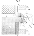
Fig. 4 is a partial amplified sectional view of an etching chamber according to an embodiment of the present invention, illustrating the process of etching the peripheral end of a wafer; -
Fig. 5 is an amplified side view of the periphery of a wafer, illustrating the result of the etching process illustrated inFig. 4 ; -
Fig. 6 is an amplified sectional view of the etching chamber illustrating the shape of the plasma varied due to the variation in the top-sided insulator, corresponding to the illustration ofFig. 4 ; -
Fig. 7 is a side view of the periphery of the wafer etched with the structure shown inFig. 6 , corresponding to the illustration ofFig. 5 ; -
Fig. 8 is an amplified sectional view of an etching chamber according to an embodiment of the present invention, illustrating the process of etching a wafer in correspondence with the illustration ofFig. 4 ; -
Fig. 9 is a variant of the etching chamber shown inFig. 8 , illustrating the process of etching a wafer in correspondence with the illustration ofFig. 4 ; -
Fig. 10 is a schematic structural view of an etching system according to an embodiment of the present invention; -
Fig. 11 is a schematic structural view of an etching system according to another embodiment of the present invention; and -
Fig. 12 is a partial amplified view of a wafer with the deposited particles at the peripheral end thereof, plasma-etched according to a prior art. - Preferred embodiments of the present invention will be now explained to make easy understanding of the advantages and the merits thereof.
-
Fig. 1 illustrates the structure of an etching chamber. - As shown in
Fig. 1 , thechamber 2 has aninner space 8 isolated from the outside by closing adoor 4 of agate 6 through which a wafer W goes in or out. Astage 10 is placed at the center of theinner space 8 to mount the wafer W thereon. - With the isolation of the
inner space 8 from the outside, the atmosphere thereof is controlled to be under the low pressure of about 10-1-10-3 Torr. - A
cathode 14 is placed at the center of the top surface of thestage 10 such that it can be elevated by anactuator 12, and connected to aplasma oscillator 16. Awater jacket 18 is provided within thestage 10 to forcefully cool it such that a coolant can be circulated via at least two paths 20 communicated with the outside. A ring-shaped bottom anode 22 is attached to the outer circumference of thestage 10 by interposing aninsulating material 23. - The
cathode 14 receives the wafer W from the top, and descends to a predetermined location to mount it on thestage 10. - At this time, the ring-
shaped bottom anode 22 should be positioned lower than the wafer W such that a predetermined distance is made between theanode 22 and the periphery of the wafer W mounted on thestage 10 to allow the discharge. - With the etching chamber according to the embodiment of the present invention, it is more preferable that the
stage 10 has the structure shown inFig. 2 . - As shown in
Fig. 2 , aninsulating plate 100 with acathode 14 is placed on thestage 10, and aplate 104 with at least threepins 102 is placed under theinsulating plate 104. Thepin 102 penetrates through theinsulating plate 100 while being protruded to the top. Theplate 104 is connected to anactuator 12 such that it can be elevated. Thecathode 14 is located at the center of the bottom surface of the insulatingplate 100. - With the above structure, the bottom surface of the wafer W is supported by the
pins 102 protruded over thestage 10, and when theactuator 12 descends, the wafer W is mounted onto the insulatingplate 100 without shaking. - As shown in
Fig. 1 , astem 24 is placed over thestage 10 with almost the same area such that it can move up and down by way of arod 26 extended upward. Furthermore, as like with thestage 10, awater jacket 28 is provided within thestem 24 such that a coolant is circulated via apath 30 communicated with the inner space of therod 26. - An
insulator 34 is attached to the bottom surface of thestem 24, and has aconcave surface 32 with a predetermined radius at the center thereof. A ring-shapedtop anode 36 is mounted around theinsulator 34 while facing thebottom anode 22. The top and thebottom anodes - Meanwhile, in case the thickness of the
insulator 34 is too thin, the discharge is liable to be made over the entire area thereof while generating plasma at the center of the wafer W, thereby making unnecessary etching. With the present invention, as the center of theinsulator 34 is spaced apart from the top surface of the wafer W with a larger distance due to the presence of theconcave portion 32, the strength of the electric field at that area becomes weak, and the discharge is not made at theconcave portion 32. - However, the relation between the thickness of the
insulator 34 and the discharge should not be disregarded. It was confirmed through experiments that when the thickness of theinsulator 34 is less than 15mm and the discharge is stably made at the periphery thereof, the discharge was also made at the center thereof even with the presence of theconcave portion 32. - In this connection, the thickness of the
insulator 34 is preferably established to be 15mm or more. - Meanwhile, a ring-shaped
reaction gas outlet 38 is placed between theinsulator 34 and thetop anode 36, and opens to blow the reaction gas injected through afirst tube passage 40 to the periphery of the wafer W. Anitrogen gas outlet 42 is placed at the centralconcave portion 32 of theinsulator 34, and opens to blow the nitrogen gas fed through asecond tube passage 44 to the center of the wafer W. Therod 26 with the first and thesecond tube passages bars 48 at its outer ends by mediating ahorizontal bar 46, and the post bars 48 are axially supported byguiders 50 provided at the outer top surface of thechamber 2 such that they move up and down without shaking. The elevation of therod 26 is made byball screws 52 and a steppingmotor 54 in synchronization with thehorizontal bar 46. - With the etching chamber according to the embodiment of the present invention, it is more preferable that a
laser sensor 56 is provided at the outer circumference of thechamber 2 to measure the gap between the wafer W and thetop anode 36 and feedback the measurement result to a controller, thereby controlling the descending location of thestem 24 correctly. - Furthermore, with the etching chamber according to the embodiment of the present invention, it is more preferable that a plurality of radial direction-controlling
aligners 58 is equidistantly arranged around the top surface of thestage 10 in thespace 8. - As shown in
Fig. 3 , thealigners 58 are formed each with apiston rod 582 moving forward and backward by way of acylinder 580. Thepiston rods 582 are elongated all with the same length while slightly holding or pressing the periphery of the wafer W to align the center thereof. In this way, the wafer W is corrected to its proper posture, and finally, the orientation flat (OF) locations thereof agree to each other. - With the etching chamber according to the embodiment of the present invention, as the top and the bottom portions of the peripheral end of the wafer W are spaced apart from the top and the
bottom anodes - That is, the nitrogen gas blown through the
nitrogen gas outlet 42 makes formation of an air curtain at the center of the wafer W, and prevents the reaction radicals generated at the periphery of the wafer W during the etching from flowing to the center thereof. - Meanwhile, as the reaction gas blown through the
reaction gas outlet 38, such as argon, CF4 and SF6, pervades to the periphery of the wafer W, the plasma is generated only at the periphery thereof. - When radio frequency is applied to the
cathode 14, as shown inFig. 4 , the reaction gas blown through thereaction gas outlet 38, more specifically, CF4 is ionized due to the discharge made only at the periphery of the wafer W, and in this condition, the dissociation reaction of CF4->CF3+F* or CF4->CF2+2F* is made. The neutral F radicals R collide against the peripheral surface of the wafer W, and react with the particles deposited thereon to thereby form volatile compounds. In this way, the etching is made, and at the same time, the reaction gas is continuously flown in the direction of the arrow of the drawing. - When the plasma Ps is generated by the reaction gas, a space charge sheath S supervening to the gas ionization is formed therein. Any discharge is not made at the space charge sheath S, the plasma is not generated. Accordingly, as the neutral F radical R is not generated, the etching at the space charge sheath S is not made.
- Meanwhile, the thickness of the space charge sheath S may be minimized by controlling the vacuum degree of the
chamber 2 and the radio frequency oscillating degree in such a way as to not hinder the plasma etching, but the influence thereof cannot be completely removed. -
Fig. 5 illustrates the result of etching the periphery of a wafer W using the etching chamber according to the embodiment of the present invention. - The etching boundary at the peripheral end of the wafer W is formed with an inclined side Ws with an etching angle θ due to the influence of the space charge sheath S. The etched area and the particles P deposited at the end thereof are indicated by the dotted line.
- Practically, even if the thickness of the space charge sheath S is controlled to be minimized, the etching angle θ reaches 2-3°, at which the wafer device is not damaged.
- In order to approximate the etching angle θ to zero, as shown in
Fig. 6 , agroove 64 is formed at the outer circumference of theinsulator 34 parallel to the wafer W. - With the formation of the
groove 64 at theinsulator 34, as shown in the drawing, the reaction gas ridden along the outer circumference thereof meets the inner circumference of thegroove 64, and is inflected along thegroove 64 so that the plasma is diffused while generating neutral F radicals R. The neutral F radicals R transmit the lower-sided space charge sheath S, and collide against the wafer W perpendicular to the surface thereof. Consequently, as shown inFig. 7 , an optimum etching shape is made such that the etching boundary is nearly vertical to the periphery of the wafer W while being positioned slightly internal to the end thereof. - Practically, it turned out that the optimum depth D of the
groove 64 was 1.8mm. - The above-described structure according to the embodiment of the present invention includes the components of a
cathode 14 and a pair ofanodes -
Fig. 8 illustrates an etching chamber according to another embodiment of the present invention where the same components as those with the etching chamber according to the previous embodiment are indicated by like reference numerals. - In this embodiment, a ring-shaped
bottom cathode 66 is attached to the outer circumference of astage 10 instead of the ring-shapedbottom anode 22, and connected to aplasma oscillator 16. A view-ring 68 is attached external to atop anode 36 to inhibit the diffusion of the reaction gas. - The view-
ring 68 mechanically shields the ring-shapedanode 36 and thebottom cathode 66 such that the reaction gas is converged without diffusing to the outside, and flown via the bottom surface of the periphery of the wafer W. In this way, the plasma Ps is sufficiently generated throughout the top to the bottom sides of the wafer W. - With the structure having the view-
ring 68, the flow pressure of the reaction gas can be controlled by properly establishing the distance G between the inner circumference of theviewing 68 and the outer circumference of the ring-shapedcathode 66. In this structure, the plasma can be generated even with a lower power by limiting the plasma-generated region. - Even in this embodiment, a
groove 64 may be formed at the outer circumference of theinsulator 34 for the same purpose as with the previous embodiment. - As shown in
Fig. 9 , thegroove 64 is formed at the outer circumference of theinsulator 34 with the omission of the view-ring 68, thereby achieving the desired etching function. - When the discharge is made between the ring-shaped
top anode 36 and the ring-shapedbottom cathode 66 facing each other to thereby generate the plasma Ps, the reaction gas flown through thereaction gas outlet 38 is diffused while making a weak flow so that the etching for the peripheral end of the wafer W may be insufficient. However, the optimum etching region based on the point of inflection of the space charge sheath S induced by thegroove 64 agrees to the peripheral end of the wafer W to thereby etch the peripheral end of the wafer W in a desired manner. - With the above-structured etching chamber according to the embodiment of the present invention, the plasma-induced heat may be highly generated during the dry cleaning process, but the
stage 10 and thestem 24 have a cooling structure to dissipate such a heat. In this case, de-ionized water (ultra pure water) is preferably used as a coolant. - With the embodiments illustrated in
Figs. 8 and9 , the structural components shown inFigs. 2 and 3 may be further provided. - An etching system with the structure shown in
Fig. 10 may be realized using the etching chamber according to the embodiment of the present invention. - As shown in
Fig. 10 , the etching system includes a plurality ofchambers 2, and ahandler 70 placed front to thechambers 2. A plurality of cassette stands 72 and awafer alignment unit 74 are placed around thehandler 70. Wafers W are mounted at a cassette C, and delivered to any one of the cassette stands 72. - In this case, the
cassette stand 72 is preferably rotated at a predetermined angle with a driving member controlled by a sensor (not shown) such that thehandler 70 takes the wafers W from the cassette C with balanced posture. - A non-safety area is established around the cassette stands 72, and a
body sensor 76 is provided there. When the worker body partially enters the non-safety area during the driving of thehandler 70, thebody sensor 76 senses it, and stops the operation of thehandler 70. - The
handler 70 takes wafers W from the cassette C, and brings them to thewafer alignment unit 74. Thewafer alignment unit 74 is rotated at a predetermined angle by the driving member, and aligns the wafers W to the inlets of thechambers 2, that is, the OF locations. - The wafers W aligned by the
wafer alignment unit 74 are taken by thehandler 70, and charged into thechambers 2 through thegates 6 thereof, followed by mounting them onto thestages 10. - The wafers W mounted on the
stage 10 is finally aligned to the OF location by thealigner 58, and when thedoor 4 of thegate 6 closes, theinner space 8 of thechamber 2 is isolated from the outside while being kept to be in a vacuum state. Thereafter, the top-sided stem 24 descends such that it is located over the wafer W by a predetermined height. - The descending of the
stem 24 is measured by alaser sensor 56, and the distance between thestem 24 and the wafer W is controlled to be optimal for the etching. When thestem 24 goes too far, the operation of thestem 24 is stopped while issuing a warning or alarm signal. - When the
stem 24 descends to a predetermined location, a nonvolatile gas and a reaction gas are fed to the wafer W from the outside so that the peripheral end of the wafer W is etched. - When the etching is terminated, the
stem 24 ascends to return to the initial location, and thedoor 4 opens. Thehandler 70 recovers the etched wafer W, and loads it onto the cassette C. The recovered wafers W are delivered to the location for the subsequent process. - The testing of the non-defective or the defective of the wafers W is conducted through the way of usual samplings.
- The
reference numeral 78 ofFig. 10 indicates a refrigerator for supplying a coolant to thechamber 2 and circulating it, and thereference numeral 80 indicates a power matcher disposed between thechamber 2 and theplasma oscillator 16. Therefrigerator 78 and thepower matcher 80 are provided per eachchamber 2. Alternatively, they may be common to all of thechambers 2 as a single unit. -
Fig. 11 illustrates an etching system according to another embodiment of the present invention. As shown inFig. 11 , a plurality ofchambers 2 are arranged around thehandler 70, and a plurality ofload lock chambers 82 are provided at the inlet and the outlet of thehandler 70. A plurality ofload ports 84 are continuously arranged close to theload lock chambers 82. The wafers W are delivered between theload lock chambers 82 and theload ports 84 by way of asubsidiary handler 86, and before they are charged into theload lock chambers 82, they are corrected in their postures by analigner 88. - With the system according to the embodiment of the present invention, the charging, taking out and the posture correction of the wafer W are conducted by the handler and the aligner as like with the previous embodiment, but a large number of
chambers 2 may be arranged, and the dry cleaning of the wafer may be automatically conducted by the collective process of sequential controlling. - With the inventive process of dry-etching the particles deposited at the peripheral end of the wafer during the dry cleaning process, the top, the lateral and the bottom sides of the periphery of the wafer are etched with a single process, or the peripheral end of the wafer is correctly etched.
- Accordingly, the target portion of the periphery of the wafer can be etched within a short period of time, and the processing efficiency per the unit time is heightened. This serves to reduce the production cost of the semiconductor device. In addition, with the omission of the conventional wet cleaning, the processing steps can be simplified.
- Although preferred embodiments of the present invention have been described in detail hereinabove, it should be clearly understood that many variations and/or modifications of the basic inventive concept herein taught which may appear to those skilled in the art will still fall within scope of the present invention, as defined in the appended claims.
Claims (8)
- A plasma etching chamber (2) adapted to etch only the periphery of a wafer by mounting the wafer on a stage (10) such that the periphery of the wafer is positioned between ring-shaped top and bottom electrodes, blowing a nitrogen gas to the center of the wafer through the center of a top-sided stem (24) while making a non-discharged region, and blowing a reaction gas to the periphery of the stem (24) to make a gas discharge, the plasma etching chamber (2) comprising:a stage (10) and a cathode (14) mounted within the stage (10) to apply radio frequency to the wafer;a ring-shaped bottom anode (22) placed at the outer circumference of the stage (10) while being positioned lower than the periphery of the wafer;a stem (24) installed over the stage (10) such that the stem (24) moves up and down;an insulator (34) attached to the bottom surface of the stem (24) with a concave portion (32), the concave portion (32) being formed at the center of the bottom surface of the stem (24) while facing the top surface of the stage (10); anda ring-shaped top anode (36) placed at the outer circumference of the insulator (34) while interposing a reaction gas outlet (38) such that a plasma is generated between the periphery of the wafer and the ring-shaped top and bottom anodes (36, 22);characterized in that a groove (64) is formed at the periphery of the insulator (34) to make a point of inflection in the flow of the reaction gas.
- The plasma etching chamber (2) of claim 1 wherein the thickness of the insulator (34) is established to be 15mm or more.
- The plasma etching chamber (2) of claim 1 further comprising an insulating plate (100) covering the top surface of the stage (10), at least three vertical pins (102) protruding from the bottom of the insulating plate (100) to the top thereof, and a plate (104) for elevating the vertical pins (102).
- The plasma etching chamber (2) of claim 1 wherein the depth of the groove (64) is established to be 1.8mm.
- The plasma etching chamber (2) of claim 1 further comprising a laser sensor (56) for measuring the distance between the ring-shaped top anode (36) and the top surface of the wafer.
- The plasma etching chamber (2) of claim 1 further comprising aligners (58) with cylinders (580) equidistantly arranged around the stage (10) and piston rods (582) elongated by the same length provided per the respective cylinders (580).
- A plasma etching system comprising:a plurality of cassette stands (72) for receiving wafer-loaded cassettes;a wafer alignment unit (74) for correcting the posture of the wafers taken from the cassettes before the chamber-charging of the wafers to align the orientation flat locations thereof;a plurality of chambers for plasma-etching the periphery of the charged wafers; anda handler (70) for conducting the charging and the taking-out of the wafers,wherein the plurality of chambers is the plasma etching chamber (2) of claim 1.
- A plasma etching system comprising:a plurality of load ports (84) for receiving the wafer-loaded cassettes;a wafer alignment unit (74) for correcting the posture of the wafers taken from the cassettes before the chamber-charging of the wafers to align the orientation flat locations thereof;a plurality of load lock chambers (82) for temporarily receiving the posture-corrected wafers or the etched wafers;a subsidiary handler for delivering the wafers among the load ports, the wafer alignment unit and the load lock chambers (82);a plurality of chambers for plasma-etching the periphery of the wafers; anda handler (70) for taking the wafers from the load lock chambers (82) to charge the wafers into the chambers, and taking the etched wafers from the chambers to return the wafers to the load lock chambers (82),wherein the plurality of chambers for plasma-etching the periphery of the wafers is the plasma etching chamber (2) of claim 1.
Applications Claiming Priority (3)
| Application Number | Priority Date | Filing Date | Title |
|---|---|---|---|
| KR20030029783 | 2003-05-12 | ||
| KR2003029783 | 2003-05-12 | ||
| PCT/KR2003/002478 WO2004100247A1 (en) | 2003-05-12 | 2003-11-18 | Plasma etching chamber and plasma etching system using same |
Publications (3)
| Publication Number | Publication Date |
|---|---|
| EP1560262A1 EP1560262A1 (en) | 2005-08-03 |
| EP1560262A4 EP1560262A4 (en) | 2007-08-15 |
| EP1560262B1 true EP1560262B1 (en) | 2017-08-23 |
Family
ID=33432432
Family Applications (1)
| Application Number | Title | Priority Date | Filing Date |
|---|---|---|---|
| EP03774252.5A Expired - Lifetime EP1560262B1 (en) | 2003-05-12 | 2003-11-18 | Plasma etching chamber and plasma etching system using same |
Country Status (7)
| Country | Link |
|---|---|
| US (1) | US7615131B2 (en) |
| EP (1) | EP1560262B1 (en) |
| JP (1) | JP4122004B2 (en) |
| KR (2) | KR100583418B1 (en) |
| CN (1) | CN100397589C (en) |
| AU (1) | AU2003284723A1 (en) |
| WO (1) | WO2004100247A1 (en) |
Families Citing this family (73)
| Publication number | Priority date | Publication date | Assignee | Title |
|---|---|---|---|---|
| KR100532354B1 (en) * | 2004-05-31 | 2005-11-30 | 삼성전자주식회사 | Apparatus for controling etching area and apparatus and method for etching edge of wafer |
| KR100635377B1 (en) | 2004-08-10 | 2006-10-17 | 세메스 주식회사 | Board Edge Etching Device |
| KR100646413B1 (en) | 2004-08-12 | 2006-11-15 | 세메스 주식회사 | Substrate Edge Etching Apparatus and Method |
| KR100598915B1 (en) * | 2005-03-28 | 2006-07-10 | 세메스 주식회사 | Substrate Edge Etching Device Using Microwave |
| KR101149332B1 (en) * | 2005-07-29 | 2012-05-23 | 주성엔지니어링(주) | Etching apparatus using the plasma |
| KR101218114B1 (en) * | 2005-08-04 | 2013-01-18 | 주성엔지니어링(주) | Etching apparatus using the plasma |
| US20070068623A1 (en) * | 2005-09-27 | 2007-03-29 | Yunsang Kim | Apparatus for the removal of a set of byproducts from a substrate edge and methods therefor |
| US8083890B2 (en) * | 2005-09-27 | 2011-12-27 | Lam Research Corporation | Gas modulation to control edge exclusion in a bevel edge etching plasma chamber |
| US7909960B2 (en) * | 2005-09-27 | 2011-03-22 | Lam Research Corporation | Apparatus and methods to remove films on bevel edge and backside of wafer |
| US8475624B2 (en) * | 2005-09-27 | 2013-07-02 | Lam Research Corporation | Method and system for distributing gas for a bevel edge etcher |
| KR101249247B1 (en) | 2005-12-21 | 2013-04-01 | 참엔지니어링(주) | Plasma etching chamber |
| US20070215049A1 (en) * | 2006-03-14 | 2007-09-20 | Applied Materials, Inc. | Transfer of wafers with edge grip |
| JP4410771B2 (en) * | 2006-04-28 | 2010-02-03 | パナソニック株式会社 | Bevel etching apparatus and bevel etching method |
| US7575638B2 (en) * | 2007-02-02 | 2009-08-18 | Lam Research Corporation | Apparatus for defining regions of process exclusion and process performance in a process chamber |
| US9184043B2 (en) * | 2006-05-24 | 2015-11-10 | Lam Research Corporation | Edge electrodes with dielectric covers |
| US7938931B2 (en) * | 2006-05-24 | 2011-05-10 | Lam Research Corporation | Edge electrodes with variable power |
| WO2008005517A1 (en) * | 2006-07-07 | 2008-01-10 | Accretech Usa, Inc. | Processing chamber having labyrinth seal |
| US7718542B2 (en) * | 2006-08-25 | 2010-05-18 | Lam Research Corporation | Low-k damage avoidance during bevel etch processing |
| US20080128088A1 (en) * | 2006-10-30 | 2008-06-05 | Jusung Engineering Co., Ltd. | Etching apparatus for edges of substrate |
| KR100823302B1 (en) * | 2006-12-08 | 2008-04-17 | 주식회사 테스 | Plasma processing equipment |
| US20080277064A1 (en) * | 2006-12-08 | 2008-11-13 | Tes Co., Ltd. | Plasma processing apparatus |
| KR100978754B1 (en) * | 2008-04-03 | 2010-08-30 | 주식회사 테스 | Plasma processing equipment |
| US20080156772A1 (en) * | 2006-12-29 | 2008-07-03 | Yunsang Kim | Method and apparatus for wafer edge processing |
| US8398778B2 (en) * | 2007-01-26 | 2013-03-19 | Lam Research Corporation | Control of bevel etch film profile using plasma exclusion zone rings larger than the wafer diameter |
| US8580078B2 (en) | 2007-01-26 | 2013-11-12 | Lam Research Corporation | Bevel etcher with vacuum chuck |
| US7858898B2 (en) * | 2007-01-26 | 2010-12-28 | Lam Research Corporation | Bevel etcher with gap control |
| US7943007B2 (en) * | 2007-01-26 | 2011-05-17 | Lam Research Corporation | Configurable bevel etcher |
| US8268116B2 (en) | 2007-06-14 | 2012-09-18 | Lam Research Corporation | Methods of and apparatus for protecting a region of process exclusion adjacent to a region of process performance in a process chamber |
| CN101241854B (en) * | 2007-02-06 | 2011-06-01 | 中芯国际集成电路制造(上海)有限公司 | A wafer production technology |
| US8137501B2 (en) * | 2007-02-08 | 2012-03-20 | Lam Research Corporation | Bevel clean device |
| CN101627461B (en) * | 2007-03-05 | 2012-01-11 | 朗姆研究公司 | Edge electrodes with variable power |
| KR101357698B1 (en) * | 2007-04-12 | 2014-02-04 | (주)소슬 | System and method for treating substrates |
| WO2008108604A1 (en) * | 2007-03-08 | 2008-09-12 | Sosul Co., Ltd. | Apparatus and method of processing substrates |
| KR101317160B1 (en) * | 2007-03-08 | 2013-10-11 | 램 리써치 코포레이션 | Plasma etching apparatus, plasma etching system and method of etching a substrate using the same |
| US8888950B2 (en) | 2007-03-16 | 2014-11-18 | Charm Engineering Co., Ltd. | Apparatus for plasma processing and method for plasma processing |
| JP2008243937A (en) * | 2007-03-26 | 2008-10-09 | Tokyo Electron Ltd | Substrate processing apparatus and substrate processing method |
| US8069817B2 (en) * | 2007-03-30 | 2011-12-06 | Lam Research Corporation | Showerhead electrodes and showerhead electrode assemblies having low-particle performance for semiconductor material processing apparatuses |
| TWI404165B (en) | 2007-04-02 | 2013-08-01 | Sosul股份有限公司 | Substrate supporting device and plasma etching device comprising the same |
| KR101342989B1 (en) * | 2007-05-03 | 2013-12-18 | (주)소슬 | Equipment for etching substrate edge |
| WO2008156366A1 (en) * | 2007-06-21 | 2008-12-24 | Asml Netherlands B.V. | Clamping device and object loading method |
| KR101412620B1 (en) * | 2007-06-28 | 2014-06-26 | 램 리써치 코포레이션 | Plasma etching equipment |
| US7981307B2 (en) * | 2007-10-02 | 2011-07-19 | Lam Research Corporation | Method and apparatus for shaping gas profile near bevel edge |
| KR101380861B1 (en) * | 2007-11-09 | 2014-04-03 | 참엔지니어링(주) | Plasma etching chamber |
| JP5184644B2 (en) * | 2007-11-21 | 2013-04-17 | ラム リサーチ コーポレーション | Bevel plasma treatment to enhance wet edge cleaning |
| KR20100099094A (en) * | 2007-12-27 | 2010-09-10 | 램 리써치 코포레이션 | Copper discoloration prevention following bevel etch process |
| KR101432562B1 (en) * | 2007-12-31 | 2014-08-21 | (주)소슬 | Substrate processing apparatus and substrate processing method |
| US20110049100A1 (en) * | 2008-01-16 | 2011-03-03 | Charm Engineering Co., Ltd. | Substrate holder, substrate supporting apparatus, substrate processing apparatus, and substrate processing method using the same |
| KR101433769B1 (en) * | 2008-02-05 | 2014-08-25 | (주)소슬 | Semiconductor manufacture equipment for bevel etch |
| KR101404010B1 (en) * | 2008-03-06 | 2014-06-12 | 주성엔지니어링(주) | Substrate edge etching apparatus and substrate edge etching method using the same |
| KR101402235B1 (en) * | 2008-04-04 | 2014-05-30 | (주)소슬 | Substrate processing appratus and method for treating subtrate |
| KR101413525B1 (en) * | 2008-04-04 | 2014-07-01 | (주)소슬 | Substrate processing appratus and method for treating subtrate |
| US8257503B2 (en) | 2008-05-02 | 2012-09-04 | Lam Research Corporation | Method and apparatus for detecting plasma unconfinement |
| US8501283B2 (en) * | 2010-10-19 | 2013-08-06 | Lam Research Corporation | Methods for depositing bevel protective film |
| US20130098390A1 (en) * | 2011-10-25 | 2013-04-25 | Infineon Technologies Ag | Device for processing a carrier and a method for processing a carrier |
| CN102956432B (en) * | 2012-10-19 | 2015-07-22 | 京东方科技集团股份有限公司 | Atmospheric-pressure plasma processing device of display substrate |
| KR101925581B1 (en) | 2012-11-23 | 2018-12-05 | 주식회사 원익아이피에스 | Method for chamber cleaning |
| CN103545164B (en) * | 2013-10-30 | 2016-06-15 | 大连理工大学 | A radio frequency plasma reaction chamber |
| JP2015233064A (en) * | 2014-06-09 | 2015-12-24 | 東京エレクトロン株式会社 | Etching processing method and bevel etching device |
| US9633862B2 (en) * | 2015-08-31 | 2017-04-25 | Kabushiki Kaisha Toshiba | Semiconductor manufacturing apparatus and semiconductor manufacturing method |
| US11251019B2 (en) * | 2016-12-15 | 2022-02-15 | Toyota Jidosha Kabushiki Kaisha | Plasma device |
| JP6863199B2 (en) | 2017-09-25 | 2021-04-21 | トヨタ自動車株式会社 | Plasma processing equipment |
| CN109392853B (en) * | 2018-11-19 | 2024-08-13 | 中国科学院南京地理与湖泊研究所 | Automatic fish electric catching scientific investigation device |
| CN113710377B (en) * | 2019-04-30 | 2024-01-09 | 迪睿合株式会社 | Method for supplying or removing the sliding treatment object to the surface of the sliding object |
| CN112992637B (en) * | 2019-12-02 | 2025-06-10 | Asmip私人控股有限公司 | Substrate support plate, substrate processing apparatus including the same, and substrate processing method |
| KR102396431B1 (en) | 2020-08-14 | 2022-05-10 | 피에스케이 주식회사 | Substrate processing apparatus and substrate transfer method |
| JP7489896B2 (en) * | 2020-10-22 | 2024-05-24 | 東京エレクトロン株式会社 | Plasma Processing Equipment |
| CN112863992B (en) * | 2021-01-12 | 2023-01-17 | 广东中图半导体科技股份有限公司 | Plasma etching device |
| KR102580583B1 (en) * | 2021-08-10 | 2023-09-21 | 피에스케이 주식회사 | Substrate processing apparatus |
| KR102929474B1 (en) * | 2021-11-22 | 2026-02-24 | 세메스 주식회사 | Apparatus for treating substrate |
| JP2024070682A (en) * | 2022-11-11 | 2024-05-23 | 東京エレクトロン株式会社 | Plasma processing apparatus and plasma processing method |
| CN115954302B (en) * | 2023-02-03 | 2023-11-14 | 北京北方华创微电子装备有限公司 | Crystal edge etching equipment |
| KR20240139355A (en) * | 2023-03-14 | 2024-09-23 | 피에스케이 주식회사 | Substrate processing apparatus and control method for substrate processing apparatus |
| KR20240154309A (en) * | 2023-04-18 | 2024-10-25 | 피에스케이 주식회사 | A substrate processing apparatus |
Citations (2)
| Publication number | Priority date | Publication date | Assignee | Title |
|---|---|---|---|---|
| EP0714998A2 (en) * | 1994-11-30 | 1996-06-05 | Applied Materials, Inc. | CVD processing chamber |
| KR20020080955A (en) * | 2001-04-18 | 2002-10-26 | (주)소슬 | plasma etching device |
Family Cites Families (9)
| Publication number | Priority date | Publication date | Assignee | Title |
|---|---|---|---|---|
| JPH07142449A (en) | 1993-11-22 | 1995-06-02 | Kawasaki Steel Corp | Plasma etching equipment |
| JP3521587B2 (en) * | 1995-02-07 | 2004-04-19 | セイコーエプソン株式会社 | Method and apparatus for removing unnecessary substances from the periphery of substrate and coating method using the same |
| DE19622015A1 (en) * | 1996-05-31 | 1997-12-04 | Siemens Ag | Process for etching destruction zones on a semiconductor substrate edge and etching system |
| US5848670A (en) * | 1996-12-04 | 1998-12-15 | Applied Materials, Inc. | Lift pin guidance apparatus |
| US6146463A (en) * | 1998-06-12 | 2000-11-14 | Applied Materials, Inc. | Apparatus and method for aligning a substrate on a support member |
| JP4055880B2 (en) * | 1999-06-02 | 2008-03-05 | 東京エレクトロン株式会社 | Plasma processing apparatus, plasma processing monitoring window member, and electrode plate for plasma processing apparatus |
| US6770166B1 (en) * | 2001-06-29 | 2004-08-03 | Lam Research Corp. | Apparatus and method for radio frequency de-coupling and bias voltage control in a plasma reactor |
| JP2002324829A (en) | 2001-07-13 | 2002-11-08 | Tokyo Electron Ltd | Processing system |
| KR100442194B1 (en) * | 2002-03-04 | 2004-07-30 | 주식회사 씨싸이언스 | Electrodes For Dry Etching Of Wafer |
-
2003
- 2003-11-18 CN CNB2003801004688A patent/CN100397589C/en not_active Expired - Lifetime
- 2003-11-18 AU AU2003284723A patent/AU2003284723A1/en not_active Abandoned
- 2003-11-18 EP EP03774252.5A patent/EP1560262B1/en not_active Expired - Lifetime
- 2003-11-18 JP JP2004571595A patent/JP4122004B2/en not_active Expired - Lifetime
- 2003-11-18 WO PCT/KR2003/002478 patent/WO2004100247A1/en not_active Ceased
- 2003-11-18 US US10/514,609 patent/US7615131B2/en not_active Expired - Lifetime
-
2004
- 2004-02-27 KR KR1020047002945A patent/KR100583418B1/en not_active Expired - Lifetime
- 2004-03-04 KR KR20-2004-0005789U patent/KR200349874Y1/en not_active Ceased
Patent Citations (2)
| Publication number | Priority date | Publication date | Assignee | Title |
|---|---|---|---|---|
| EP0714998A2 (en) * | 1994-11-30 | 1996-06-05 | Applied Materials, Inc. | CVD processing chamber |
| KR20020080955A (en) * | 2001-04-18 | 2002-10-26 | (주)소슬 | plasma etching device |
Also Published As
| Publication number | Publication date |
|---|---|
| EP1560262A1 (en) | 2005-08-03 |
| US7615131B2 (en) | 2009-11-10 |
| US20050173067A1 (en) | 2005-08-11 |
| WO2004100247A1 (en) | 2004-11-18 |
| EP1560262A4 (en) | 2007-08-15 |
| KR200349874Y1 (en) | 2004-05-12 |
| KR20050008637A (en) | 2005-01-21 |
| JP4122004B2 (en) | 2008-07-23 |
| CN100397589C (en) | 2008-06-25 |
| CN1692475A (en) | 2005-11-02 |
| AU2003284723A1 (en) | 2004-11-26 |
| JPWO2004100247A1 (en) | 2006-07-13 |
| KR100583418B1 (en) | 2006-05-25 |
Similar Documents
| Publication | Publication Date | Title |
|---|---|---|
| US7615131B2 (en) | Plasma etching chamber and plasma etching system using same | |
| US9251998B2 (en) | Plasma processing apparatus | |
| US6969669B2 (en) | Method of manufacturing semiconductor device and cutting apparatus for cutting semiconductor wafer | |
| US9293568B2 (en) | Method of fin patterning | |
| US11295933B2 (en) | Substrate processing apparatus and substrate processing method | |
| US20050178505A1 (en) | Electrode for dry etching a wafer | |
| TWI543252B (en) | Apparatus and method for power measurement in plasma etcher | |
| US8123901B2 (en) | Etching apparatus | |
| US20050039854A1 (en) | Plasma etching method and plasma etching unit | |
| TWI605510B (en) | Apparatus and method for concentrated plasma | |
| KR100283425B1 (en) | Metal wiring formation process and system of semiconductor device | |
| US20250046629A1 (en) | Ion beam etching apparatus, method for manufacturing semiconductor device using the same, and method for treating substrate using the same | |
| US20060118517A1 (en) | Etching method | |
| US20240379330A1 (en) | Gas distribution ring for process chamber | |
| KR100851237B1 (en) | Substrate Processing Method | |
| KR20150116003A (en) | Apparatus, system, and metho for treating substrate | |
| US20260144008A1 (en) | Semiconductor manufacturing device and teaching apparatus including the same | |
| US6723651B2 (en) | Plasma processing method | |
| JP2021040015A (en) | Nozzle plasma device | |
| US20240412958A1 (en) | Plasma processing apparatus and method of manufacturing semiconductor device | |
| US20230067873A1 (en) | Substrate treating apparatus and substrate treating method | |
| KR102577288B1 (en) | Apparatus for treating substrate and method thereof | |
| KR100604826B1 (en) | Plasma processing apparatus for processing wafer edges and plasma processing method thereof | |
| KR20250020257A (en) | Ion beam etching apparatus, semiconductor device manufacturing method using the same, and substrate processing method using the same | |
| CN118824829A (en) | Substrate processing equipment |
Legal Events
| Date | Code | Title | Description |
|---|---|---|---|
| PUAI | Public reference made under article 153(3) epc to a published international application that has entered the european phase |
Free format text: ORIGINAL CODE: 0009012 |
|
| 17P | Request for examination filed |
Effective date: 20041110 |
|
| AK | Designated contracting states |
Kind code of ref document: A1 Designated state(s): AT BE BG CH CY CZ DE DK EE ES FI FR GB GR HU IE IT LI LU MC NL PT RO SE SI SK TR |
|
| AX | Request for extension of the european patent |
Extension state: AL LT LV MK |
|
| DAX | Request for extension of the european patent (deleted) | ||
| A4 | Supplementary search report drawn up and despatched |
Effective date: 20070716 |
|
| 17Q | First examination report despatched |
Effective date: 20161004 |
|
| REG | Reference to a national code |
Ref country code: DE Ref legal event code: R079 Ref document number: 60350545 Country of ref document: DE Free format text: PREVIOUS MAIN CLASS: H01L0021306500 Ipc: H01J0037320000 |
|
| GRAP | Despatch of communication of intention to grant a patent |
Free format text: ORIGINAL CODE: EPIDOSNIGR1 |
|
| RIC1 | Information provided on ipc code assigned before grant |
Ipc: H01L 21/3065 20060101ALI20170321BHEP Ipc: H01J 37/32 20060101AFI20170321BHEP |
|
| INTG | Intention to grant announced |
Effective date: 20170404 |
|
| GRAS | Grant fee paid |
Free format text: ORIGINAL CODE: EPIDOSNIGR3 |
|
| GRAA | (expected) grant |
Free format text: ORIGINAL CODE: 0009210 |
|
| AK | Designated contracting states |
Kind code of ref document: B1 Designated state(s): AT BE BG CH CY CZ DE DK EE ES FI FR GB GR HU IE IT LI LU MC NL PT RO SE SI SK TR |
|
| REG | Reference to a national code |
Ref country code: GB Ref legal event code: FG4D |
|
| REG | Reference to a national code |
Ref country code: CH Ref legal event code: EP |
|
| REG | Reference to a national code |
Ref country code: AT Ref legal event code: REF Ref document number: 922181 Country of ref document: AT Kind code of ref document: T Effective date: 20170915 |
|
| REG | Reference to a national code |
Ref country code: IE Ref legal event code: FG4D |
|
| REG | Reference to a national code |
Ref country code: DE Ref legal event code: R096 Ref document number: 60350545 Country of ref document: DE |
|
| REG | Reference to a national code |
Ref country code: NL Ref legal event code: MP Effective date: 20170823 |
|
| REG | Reference to a national code |
Ref country code: AT Ref legal event code: MK05 Ref document number: 922181 Country of ref document: AT Kind code of ref document: T Effective date: 20170823 |
|
| PG25 | Lapsed in a contracting state [announced via postgrant information from national office to epo] |
Ref country code: SE Free format text: LAPSE BECAUSE OF FAILURE TO SUBMIT A TRANSLATION OF THE DESCRIPTION OR TO PAY THE FEE WITHIN THE PRESCRIBED TIME-LIMIT Effective date: 20170823 Ref country code: FI Free format text: LAPSE BECAUSE OF FAILURE TO SUBMIT A TRANSLATION OF THE DESCRIPTION OR TO PAY THE FEE WITHIN THE PRESCRIBED TIME-LIMIT Effective date: 20170823 Ref country code: NL Free format text: LAPSE BECAUSE OF FAILURE TO SUBMIT A TRANSLATION OF THE DESCRIPTION OR TO PAY THE FEE WITHIN THE PRESCRIBED TIME-LIMIT Effective date: 20170823 Ref country code: AT Free format text: LAPSE BECAUSE OF FAILURE TO SUBMIT A TRANSLATION OF THE DESCRIPTION OR TO PAY THE FEE WITHIN THE PRESCRIBED TIME-LIMIT Effective date: 20170823 |
|
| PG25 | Lapsed in a contracting state [announced via postgrant information from national office to epo] |
Ref country code: BG Free format text: LAPSE BECAUSE OF FAILURE TO SUBMIT A TRANSLATION OF THE DESCRIPTION OR TO PAY THE FEE WITHIN THE PRESCRIBED TIME-LIMIT Effective date: 20171123 Ref country code: GR Free format text: LAPSE BECAUSE OF FAILURE TO SUBMIT A TRANSLATION OF THE DESCRIPTION OR TO PAY THE FEE WITHIN THE PRESCRIBED TIME-LIMIT Effective date: 20171124 Ref country code: ES Free format text: LAPSE BECAUSE OF FAILURE TO SUBMIT A TRANSLATION OF THE DESCRIPTION OR TO PAY THE FEE WITHIN THE PRESCRIBED TIME-LIMIT Effective date: 20170823 |
|
| PG25 | Lapsed in a contracting state [announced via postgrant information from national office to epo] |
Ref country code: DK Free format text: LAPSE BECAUSE OF FAILURE TO SUBMIT A TRANSLATION OF THE DESCRIPTION OR TO PAY THE FEE WITHIN THE PRESCRIBED TIME-LIMIT Effective date: 20170823 Ref country code: CZ Free format text: LAPSE BECAUSE OF FAILURE TO SUBMIT A TRANSLATION OF THE DESCRIPTION OR TO PAY THE FEE WITHIN THE PRESCRIBED TIME-LIMIT Effective date: 20170823 Ref country code: RO Free format text: LAPSE BECAUSE OF FAILURE TO SUBMIT A TRANSLATION OF THE DESCRIPTION OR TO PAY THE FEE WITHIN THE PRESCRIBED TIME-LIMIT Effective date: 20170823 |
|
| REG | Reference to a national code |
Ref country code: DE Ref legal event code: R097 Ref document number: 60350545 Country of ref document: DE |
|
| PG25 | Lapsed in a contracting state [announced via postgrant information from national office to epo] |
Ref country code: SK Free format text: LAPSE BECAUSE OF FAILURE TO SUBMIT A TRANSLATION OF THE DESCRIPTION OR TO PAY THE FEE WITHIN THE PRESCRIBED TIME-LIMIT Effective date: 20170823 Ref country code: EE Free format text: LAPSE BECAUSE OF FAILURE TO SUBMIT A TRANSLATION OF THE DESCRIPTION OR TO PAY THE FEE WITHIN THE PRESCRIBED TIME-LIMIT Effective date: 20170823 Ref country code: IT Free format text: LAPSE BECAUSE OF FAILURE TO SUBMIT A TRANSLATION OF THE DESCRIPTION OR TO PAY THE FEE WITHIN THE PRESCRIBED TIME-LIMIT Effective date: 20170823 |
|
| REG | Reference to a national code |
Ref country code: DE Ref legal event code: R119 Ref document number: 60350545 Country of ref document: DE |
|
| PG25 | Lapsed in a contracting state [announced via postgrant information from national office to epo] |
Ref country code: MC Free format text: LAPSE BECAUSE OF FAILURE TO SUBMIT A TRANSLATION OF THE DESCRIPTION OR TO PAY THE FEE WITHIN THE PRESCRIBED TIME-LIMIT Effective date: 20170823 |
|
| PLBE | No opposition filed within time limit |
Free format text: ORIGINAL CODE: 0009261 |
|
| STAA | Information on the status of an ep patent application or granted ep patent |
Free format text: STATUS: NO OPPOSITION FILED WITHIN TIME LIMIT |
|
| GBPC | Gb: european patent ceased through non-payment of renewal fee |
Effective date: 20171123 |
|
| PG25 | Lapsed in a contracting state [announced via postgrant information from national office to epo] |
Ref country code: LI Free format text: LAPSE BECAUSE OF NON-PAYMENT OF DUE FEES Effective date: 20171130 Ref country code: CH Free format text: LAPSE BECAUSE OF NON-PAYMENT OF DUE FEES Effective date: 20171130 |
|
| 26N | No opposition filed |
Effective date: 20180524 |
|
| PG25 | Lapsed in a contracting state [announced via postgrant information from national office to epo] |
Ref country code: LU Free format text: LAPSE BECAUSE OF NON-PAYMENT OF DUE FEES Effective date: 20171118 Ref country code: SI Free format text: LAPSE BECAUSE OF FAILURE TO SUBMIT A TRANSLATION OF THE DESCRIPTION OR TO PAY THE FEE WITHIN THE PRESCRIBED TIME-LIMIT Effective date: 20170823 |
|
| REG | Reference to a national code |
Ref country code: FR Ref legal event code: ST Effective date: 20180731 Ref country code: BE Ref legal event code: MM Effective date: 20171130 |
|
| REG | Reference to a national code |
Ref country code: IE Ref legal event code: MM4A |
|
| PG25 | Lapsed in a contracting state [announced via postgrant information from national office to epo] |
Ref country code: FR Free format text: LAPSE BECAUSE OF NON-PAYMENT OF DUE FEES Effective date: 20171130 Ref country code: DE Free format text: LAPSE BECAUSE OF NON-PAYMENT OF DUE FEES Effective date: 20180602 Ref country code: IE Free format text: LAPSE BECAUSE OF NON-PAYMENT OF DUE FEES Effective date: 20171118 |
|
| PG25 | Lapsed in a contracting state [announced via postgrant information from national office to epo] |
Ref country code: GB Free format text: LAPSE BECAUSE OF NON-PAYMENT OF DUE FEES Effective date: 20171123 Ref country code: BE Free format text: LAPSE BECAUSE OF NON-PAYMENT OF DUE FEES Effective date: 20171130 |
|
| PG25 | Lapsed in a contracting state [announced via postgrant information from national office to epo] |
Ref country code: HU Free format text: LAPSE BECAUSE OF FAILURE TO SUBMIT A TRANSLATION OF THE DESCRIPTION OR TO PAY THE FEE WITHIN THE PRESCRIBED TIME-LIMIT; INVALID AB INITIO Effective date: 20031118 |
|
| PG25 | Lapsed in a contracting state [announced via postgrant information from national office to epo] |
Ref country code: CY Free format text: LAPSE BECAUSE OF NON-PAYMENT OF DUE FEES Effective date: 20170823 |
|
| PG25 | Lapsed in a contracting state [announced via postgrant information from national office to epo] |
Ref country code: TR Free format text: LAPSE BECAUSE OF FAILURE TO SUBMIT A TRANSLATION OF THE DESCRIPTION OR TO PAY THE FEE WITHIN THE PRESCRIBED TIME-LIMIT Effective date: 20170823 |
|
| PG25 | Lapsed in a contracting state [announced via postgrant information from national office to epo] |
Ref country code: PT Free format text: LAPSE BECAUSE OF FAILURE TO SUBMIT A TRANSLATION OF THE DESCRIPTION OR TO PAY THE FEE WITHIN THE PRESCRIBED TIME-LIMIT Effective date: 20170823 |