JP4122004B2 - Plasma etching chamber and plasma etching system using the same - Google Patents
Plasma etching chamber and plasma etching system using the same Download PDFInfo
- Publication number
- JP4122004B2 JP4122004B2 JP2004571595A JP2004571595A JP4122004B2 JP 4122004 B2 JP4122004 B2 JP 4122004B2 JP 2004571595 A JP2004571595 A JP 2004571595A JP 2004571595 A JP2004571595 A JP 2004571595A JP 4122004 B2 JP4122004 B2 JP 4122004B2
- Authority
- JP
- Japan
- Prior art keywords
- wafer
- ring
- insulator
- stage
- plasma etching
- Prior art date
- Legal status (The legal status is an assumption and is not a legal conclusion. Google has not performed a legal analysis and makes no representation as to the accuracy of the status listed.)
- Expired - Lifetime
Links
- 238000001020 plasma etching Methods 0.000 title claims description 29
- 230000002093 peripheral effect Effects 0.000 claims description 48
- 239000012212 insulator Substances 0.000 claims description 28
- 239000012495 reaction gas Substances 0.000 claims description 23
- 239000007789 gas Substances 0.000 claims description 10
- IJGRMHOSHXDMSA-UHFFFAOYSA-N Atomic nitrogen Chemical compound N#N IJGRMHOSHXDMSA-UHFFFAOYSA-N 0.000 claims description 9
- 229910001873 dinitrogen Inorganic materials 0.000 claims description 7
- 238000007664 blowing Methods 0.000 claims 3
- 235000012431 wafers Nutrition 0.000 description 110
- 238000005530 etching Methods 0.000 description 47
- 238000000034 method Methods 0.000 description 20
- 230000008569 process Effects 0.000 description 16
- 239000002245 particle Substances 0.000 description 14
- 239000004065 semiconductor Substances 0.000 description 8
- 238000004140 cleaning Methods 0.000 description 5
- 238000005108 dry cleaning Methods 0.000 description 4
- 239000003507 refrigerant Substances 0.000 description 4
- 230000008901 benefit Effects 0.000 description 3
- 238000012937 correction Methods 0.000 description 3
- 230000007935 neutral effect Effects 0.000 description 3
- XLYOFNOQVPJJNP-UHFFFAOYSA-N water Substances O XLYOFNOQVPJJNP-UHFFFAOYSA-N 0.000 description 3
- XKRFYHLGVUSROY-UHFFFAOYSA-N Argon Chemical compound [Ar] XKRFYHLGVUSROY-UHFFFAOYSA-N 0.000 description 2
- 239000006227 byproduct Substances 0.000 description 2
- 238000010586 diagram Methods 0.000 description 2
- 238000007599 discharging Methods 0.000 description 2
- 239000011261 inert gas Substances 0.000 description 2
- 238000012986 modification Methods 0.000 description 2
- 230000004048 modification Effects 0.000 description 2
- 238000012545 processing Methods 0.000 description 2
- -1 CF 4 Inorganic materials 0.000 description 1
- 229910052786 argon Inorganic materials 0.000 description 1
- 238000010923 batch production Methods 0.000 description 1
- 238000006243 chemical reaction Methods 0.000 description 1
- 150000001875 compounds Chemical class 0.000 description 1
- 238000001816 cooling Methods 0.000 description 1
- 230000007547 defect Effects 0.000 description 1
- 239000008367 deionised water Substances 0.000 description 1
- 229910021641 deionized water Inorganic materials 0.000 description 1
- 238000009792 diffusion process Methods 0.000 description 1
- 238000010494 dissociation reaction Methods 0.000 description 1
- 208000018459 dissociative disease Diseases 0.000 description 1
- 238000009826 distribution Methods 0.000 description 1
- 238000001312 dry etching Methods 0.000 description 1
- 230000005684 electric field Effects 0.000 description 1
- 239000003344 environmental pollutant Substances 0.000 description 1
- 238000002474 experimental method Methods 0.000 description 1
- 238000007689 inspection Methods 0.000 description 1
- 239000011810 insulating material Substances 0.000 description 1
- 238000010030 laminating Methods 0.000 description 1
- 238000004519 manufacturing process Methods 0.000 description 1
- 229910052757 nitrogen Inorganic materials 0.000 description 1
- 230000010355 oscillation Effects 0.000 description 1
- 238000000059 patterning Methods 0.000 description 1
- 231100000719 pollutant Toxicity 0.000 description 1
- 238000005070 sampling Methods 0.000 description 1
- 238000003892 spreading Methods 0.000 description 1
- 230000007480 spreading Effects 0.000 description 1
- 230000032258 transport Effects 0.000 description 1
- 229910021642 ultra pure water Inorganic materials 0.000 description 1
- 239000012498 ultrapure water Substances 0.000 description 1
Images


Classifications
-
- H—ELECTRICITY
- H01—ELECTRIC ELEMENTS
- H01L—SEMICONDUCTOR DEVICES NOT COVERED BY CLASS H10
- H01L21/00—Processes or apparatus adapted for the manufacture or treatment of semiconductor or solid state devices or of parts thereof
- H01L21/02—Manufacture or treatment of semiconductor devices or of parts thereof
- H01L21/04—Manufacture or treatment of semiconductor devices or of parts thereof the devices having at least one potential-jump barrier or surface barrier, e.g. PN junction, depletion layer or carrier concentration layer
- H01L21/18—Manufacture or treatment of semiconductor devices or of parts thereof the devices having at least one potential-jump barrier or surface barrier, e.g. PN junction, depletion layer or carrier concentration layer the devices having semiconductor bodies comprising elements of Group IV of the Periodic System or AIIIBV compounds with or without impurities, e.g. doping materials
- H01L21/30—Treatment of semiconductor bodies using processes or apparatus not provided for in groups H01L21/20 - H01L21/26
- H01L21/302—Treatment of semiconductor bodies using processes or apparatus not provided for in groups H01L21/20 - H01L21/26 to change their surface-physical characteristics or shape, e.g. etching, polishing, cutting
- H01L21/306—Chemical or electrical treatment, e.g. electrolytic etching
- H01L21/3065—Plasma etching; Reactive-ion etching
-
- H—ELECTRICITY
- H01—ELECTRIC ELEMENTS
- H01L—SEMICONDUCTOR DEVICES NOT COVERED BY CLASS H10
- H01L21/00—Processes or apparatus adapted for the manufacture or treatment of semiconductor or solid state devices or of parts thereof
- H01L21/02—Manufacture or treatment of semiconductor devices or of parts thereof
- H01L21/02041—Cleaning
- H01L21/02082—Cleaning product to be cleaned
-
- H—ELECTRICITY
- H01—ELECTRIC ELEMENTS
- H01J—ELECTRIC DISCHARGE TUBES OR DISCHARGE LAMPS
- H01J37/00—Discharge tubes with provision for introducing objects or material to be exposed to the discharge, e.g. for the purpose of examination or processing thereof
- H01J37/32—Gas-filled discharge tubes
- H01J37/32009—Arrangements for generation of plasma specially adapted for examination or treatment of objects, e.g. plasma sources
- H01J37/32082—Radio frequency generated discharge
- H01J37/32091—Radio frequency generated discharge the radio frequency energy being capacitively coupled to the plasma
-
- H—ELECTRICITY
- H01—ELECTRIC ELEMENTS
- H01J—ELECTRIC DISCHARGE TUBES OR DISCHARGE LAMPS
- H01J37/00—Discharge tubes with provision for introducing objects or material to be exposed to the discharge, e.g. for the purpose of examination or processing thereof
- H01J37/32—Gas-filled discharge tubes
- H01J37/32431—Constructional details of the reactor
- H01J37/32532—Electrodes
-
- H—ELECTRICITY
- H01—ELECTRIC ELEMENTS
- H01J—ELECTRIC DISCHARGE TUBES OR DISCHARGE LAMPS
- H01J2237/00—Discharge tubes exposing object to beam, e.g. for analysis treatment, etching, imaging
- H01J2237/32—Processing objects by plasma generation
- H01J2237/33—Processing objects by plasma generation characterised by the type of processing
- H01J2237/334—Etching
Description
【技術分野】
この発明は、半導体ウェーハの周縁端に残っている膜質と、パーティクルの洗浄に関し、更に詳しくは、プラズマで乾式エッチングしたウェーハの周縁端に残る膜質、及び、その周りに堆積されるパーティクルを、プラズマでエッチングして完璧に除去することが出来るプラズマエッチングチャンバーと、これを用いたプラズマエッチングシステ厶に関する。
【背景技術】
ウェーハの表面に膜質を積層するパタング段階において、ウェーハの周縁端にも不要に膜質が積層され、その上に、ウェーハの上面をプラズマでエッチングする乾式洗浄工程中には、エッチングにより発生する副産物(By−Product)が完全に排気されず、ウェーハの周縁端の上面から側面、及び、底面に亘って堆積されて、パーティクルとして残る。
即ち、プラズマエッチングしたウェーハは、図12に示すように、ウェーハ91の周縁端から側面、及び、底面まで連続的にパーティクル93が堆積して、ステージ95とウェーハ91との間にまで侵入する様に見えている。
通常、ウェーハの周縁部は、半導体チップにならない部分であるが、ここに残っている膜質とパーティクル(以下、パーティクルと略称する)は、以後の半導体工程で、半導体チップに深刻な損傷を引き起こす要因になるために、除去されなければならない。
ウェーハの周縁端において、上述のように堆積するパーティクルは、湿式洗浄法で取り除くことが出来るが、この方法は洗浄される半導体に新たに他の不良を引き起こす要素を持ってあり,洗浄した後に残る溶液は反応性が強くて、環境に悪い公害物質として残され、その処理も容易ではない。
日本国公開特許公報平成07ー142449号は前記ウェーハの周縁端に残存するパーティクルをプラズマでエッチングする装置を開示している。
例示された装置は、ウェーハの周縁に対応して配置した上下部電極の間に反応ガスを吹き付け、プラズマによるエッチングが行われるようにする一方、上部電極の中央部に不活性ガスを、吹き付けて、前記のように生成されるプラズマがウェーハの内側に侵入できない様にしている。
どころが、前記の装置は高周波をウェーハと対向する上部電極側に印加する構成であるために、ウェーハにはセルフーバイアスが印加されないから、エッチング速度が遅くて、工程時間も長くなる。
その上に、エッチングはウェーハの周縁の上面だけ行われて、その側面から底面に亘って堆積しているパーティクルを完全には取り除けない。
この発明の目的は、プラズマエッチングによって、ウェーハ周縁端に堆積された膜質と、パーティクルを、エッチングして取り除く場合に、ウェーハの周縁の上面から側面・底面にまで連続して完全に高効率でエッチング出来るプラズマエッチングチャンバーを提供することである.
この発明の他の目的は、前記新規なプラズマエッチングチャンバーを、半導体生産工程に適用することが出来るように、短時間内に大量のウェーハを処理することが出来るプラズマエッチングシステ厶を提供することである。
前述の目的を具現するこの発明のプラズマエッチングチャンバーは、チャンバーの内部に配置されたステージを経てウェーハに高周波(Radio−Frequency)を印加するようにカソードを設けて、前記ステージの外周縁でウェーハの周縁より低い位置にリング状の下部アノードを設けると共に、前記ステージ上方にリング状の上部アノードを、前記リング状の下部アノードに対向するように配置し、前記ウェーハ周縁端と前記リング状の上部アノードとの、及び、前記ウェーハ周縁端と前記リング状の下部アノードとの間を同時に放電させて発生するプラズマを用いて前記ウェーハ周縁の上面から底面に亘る領域を連続的にエッチングする構成を持つ。
また、この発明のエッチングチャンバーは、ステージ上に載置されるウェーハの周縁部上側と下側に、各々リング状の上部アノードと、リング状の下部カソードを対向配置し、また、前記リング状の上部アノード外周側にビューリングを設けて、プラズマ空間の拡張を制限して、前記リング状の上部アノードと前記リング状の下部カソードとの間に流れる反応ガスの圧力分布を調節して、放電により発生するプラズマが、前記ウェーハ周縁の上面から底面に亘る領域を効果的にエッチングする構成を持つ。
尚、この発明のプラズマエッチングチャンバーは、前記ステージの上方に対向配置される円盤状絶縁体の外周面にウェーハと平行に伸びる溝を形成して、エッチングの境界面が直角状になるようにすることが出来る。
また、この発明のエッチングチャンバーは、ウェーハの上方に対向配置される絶縁体の中心を、凹面に形成して、その付近での放電が抑制されるようにすることが出来る。
尚、この発明のプラズマエッチングチャンバーは、前記ステージの上面にウェーハを安定に載置するための手段、或は、最適のウェーハエッチングが実行されるようにするために、ウェーハ上面とリング状の上部アノードとの放電隙間を測定して、最適の寸法になるように、位置制御するレーザーセンサー等を、更に備えることが出来る。
また、この発明のプラズマエッチングチャンバーは、前記ステージの上に載置されるウェーハを、正しい姿勢に直すために中心を合わせるアライナーを、更に備えることが出来る。
尚、前述の目的を具現するこの発明のプラズマエッチングシステ厶は,ウェーハが収納されたカセットを、複数配列されたカセット受けのいずれか一つに供給すると、ハンドラーが前記ウェーハを取り出し、ウェーハ整列部に送り、ここでウェーハのOF(Orientation Flat)位置の姿勢矯正が行われると、再びハンドラーがウェーハを取り出して、チャンバーに装入させエッチングが行われるようにしており、ウェーハのエッチングが完了すると、ハンドラーはチャンバーからウェーハを取り出して、元のカセットに装入する過程を繰り返す。
また、この発明のプラズマエッチングシステ厶は、ウェーハが収納されたカセットをロードポートに供給すると、補助ハンドラーが前記ウェーハを取り出し、ウェーハ整列部に送ってOF位置を姿勢矯正した後、矯正されたウェーハをロードラックチャンバーへ臨時に収納すると、ハンドラーがロードラックチャンバーからウェーハを取り出して、複数配置されたチャンバーのいずれか一つに装入して、エッチングが行われるようにし、エッチングが終ると、前記ハンドラーは、ウェーハを取り出してロードラックチャンバーへ再び装入し、ロードラックチャンバーへ装入されたウェーハを前記補助ハンドラーが取り出して、元のカセットに反納する過程を繰り返す。
【図面の簡単な説明】
図1は、この発明に關するプラズマエッチングチャンバーの構造を示す側断面図。
図2は、図1のチャンバー内に設けられるステージの変形例を示す部分側断面図。
図3は、図1のチャンバー内部でステージの付近に設けられるアライナーによるウェーハの中心を合致させる整列例を示す平面図。
図4は、この発明に關するエッチングチャンバーにおいて、ウェーハ周縁端のエッチング過程を説明するための部分拡大断面図。
図5は、図4に示したエッチングの結果を説明するためにウェーハの周縁を拡大して描いた側面図。
図6は、図4に対応する図面で、上部に取り付けられる絶縁体の変形によるプラズマの変化された様子を示す拡大断面図。
図7は、図5に対応する図面で、図6に示した構成によりエッチングされたウェーハの周縁を示す側面図。
図8は、この発明に關するエッチングチャンバーの他の実施例で、図4に対応してウェーハのエッチング過程を示す拡大断面図。
図9は、図8に示した実施例の変形例で、図4に対応してウェーハのエッチング過程を示す拡大断面図。
図10は、この発明のエッチングシステ厶に関する一実施例を示す概略構成図。
図11は、この発明のエッチングシステ厶に関する他の実施例を示す概略構成図。
図12は、通常の方式によってプラズマエッチングされたウェーハの周縁端にパーティクルが堆積された様子を描く部分拡大図。
【実施例】
この発明の特徴と長所は、次の望ましい実施例によって、よく理解することが出来る。
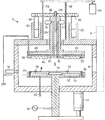
図1は、この発明に關するエッチングチャンバーの構造を描いている。
図面において、チャンバー2の内部は、ドア4により、ウェーハWが出し入れるゲート6を閉鎖させることにより、外部から隔離される空間8になって、その中央下側にはウェーハWを搭載させるためのステージ10が設けられている。
空間8の雰囲気は外部から隔離した後に、大略10−1〜10−3Torrほどの低圧に調整される。
ステージ10の上面中央には、アクチュエーター12により昇降できるカソード14が設けられ、プラズマ発振器16と接続されており、また、ステージ内部には強制冷却用のウォータージャケット18が形成され、ここから外部に開いた、少なくとも二つの通路20を経て、冷媒が循環出来るようになっており、ステージ外周部にはリング状の下部アノード22が絶縁材23を介して取り付けられている。
カソード14は上方から供給されるウェーハWを受け取った後に、一定位置まで降下して前記ステージ10の上端にウェーハを載せるように動作する。
この時、リング状の下部アノード22の位置は、ステージ10に載せられたウェーハWの周縁との間に、放電に要する所定の隙間ができるように、前記ウェーハWより低く配置しなければならない。
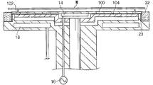
この発明によるエッチングチャンバーにおいて、更に望ましいことは、ステージ10を図2に示した構造にすることである。
図2に例示されたステージ10の上面には、カソード14を備えた絶縁板100があり、その下方には、少なくとも三つのピン102を備えたプレート104があって、前記ピン102は絶縁板100を貫いて上方に出没自在に配置され、また、プレート104は前記アクチュエーター12と連結されて昇降出来る構造を持ち、このような構造の場合にカソード14は、前記絶縁板100の下面中央に設けられる。
上述の構造は、ステージ10の上に突出しているピン102で、ウェーハWの底面を支えるように受けて、次にアクチュエーター12が降下すれば、揺れずにウェーハWを絶縁板100の上に載せる作用をする。
また、図1を参照すれは、ステージ10の上方には、これと殆んど同じ平面積を持つステム24が、上方に伸びたロッド26により、上下に昇降自在に配置されており、また、ステム24の内部にもステージ10と同様にウォータージャケット28が設けられて、前記ロッド26の内部に開いている通路30を経て冷媒が循環する。
ステム24の底面には、中央に所定半径の凹面32を形成した絶縁体34が取り付けられており、その周りにはリング状の上部アノード36が、下部アノード22と対向するように配置されて、これらの上下部アノード36、22は両者共に接地されている。
一方、絶縁体34の厚さがあまり薄ければ、その全面に亘って放電が起きて、これによってウェーハWの中心部にもプラズマが発生し、不要エッチングをする恐れがあるが、この発明では凹部32により、絶縁体34の中央部が、他の部分よりウェーハWの上面と対峙する隙間が大きいから電気場の強さが弱くなって、凹部32には放電が起きない。
しかしながら、絶縁体34の厚さと、放電との関係も無視出来ないことで、実験によれば、絶縁体34の厚さが15mm未満の時に、周縁部で安定に放電する状況では、凹部32があるにも関わらず中央部でも放電が起きることを確認した。
従って、絶縁体34の厚さは15mm以上にすることがよい。
一方、絶縁体34と上部アノード36との間は反応ガス出口38がリング状に開いて、第1管路40を経て注入される反応ガスを、ウェーハWの周縁に吹き付けるようになっていると共に、中心側凹部32には、窒素ガス出口42が開いて、第2管路44を経て注入される窒素ガスを前記ウェーハWの中心に吹き付けるようになっている。
第1及び、第2管路40、44を備えた前記ロッド26は、その外側端が水平バー46を介してポストバー48と連結され、また、ポストバー48はチャンバー2の外部の上側に設けられたガイダ50の軸支えにより揺れないで昇降するようになる。また、ロッド26の昇降動作は前記水平バー46を連動させるボールスクリュー52と、ステッピングモータ54によって行われる。
この発明によるエッチングチャンバーは、更に望ましくは、チャンバー2の外周の一側にレーザーセンサー56を備えており、そのセンサー56はウェーハWと、上部アノード36のギャップを測定して、コントローラにフィドバックさせることにより、前記ステム24の降下位置を正確に制御することが出来る。
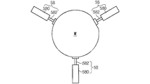
また、この発明によるエッチングチャンバーは、更に望ましくは、空間8の内部でステージ10の上端面の周りに等分配置される複数の半径方向調整用アライナー58を備えている。
前記アライナー58は、図3に示したように、シリンダ580により進退するピストンロッド582で構成され、前記ピストンロッド582は、全て同じ長さで伸長されながらウェーハWの外周を、軽く捕捉または押圧することにより中心位置を合わせて、前記ウェーハWは正しい姿勢に矯正され、最後にOF位置を合わせるようになる。
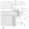
この発明のエッチングチャンバーによると、ウェーハWの周縁端の上面から底面に至る一定部位が各々上下部アノード36、22との間に、所定の隙間を置いて対峙することになるので、この部分のみにプラズマを発生させることが出来る。
即ち、窒素ガスの出口42から吹き出される窒素ガスは、ウェーハWの中心部でエアカーテンを形成して、エッチング時にウェーハの周縁から生成される反応基らが、前記ウェーハの中心部へ流れ込むことを防ぐようになる。また一方には、反応ガス出口38から吹き出される反応ガス、例えば、アルゴン、CF4、SF6は、前記ウェーハWの周縁に経て流れ広がるために、プラズマはウェーハの周縁のみに生成される。
この時、カソード14に高周波を印加すると、図4に示したように、ウェーハWの周縁端のみに行われる放電によって、反応ガス出口38から流れ出す反応ガス、更に詳しくは、反応ガスCF4はイオン化され、この条件で、CF4→CF3+F*、若しくはCF4→CF2+2F*等が、解離反応により生成され、中性FラジカルRが、前記ウェーハWの周縁の表面に衝突して、このところに堆積しているパーティクルと表面で反応して、揮発性化合物に変換させる過程を通じて、エッチングが進められ、これと同時に反応ガスは続けて図面の矢印方向に流れる。
前記反応ガスにより、ウェーハの周縁端にプラズマ(Ps)が発生する時に、ウェーハの内部側は凹面(32)によって隙間が広がり、また、放電が難い窒素のような分子状多原子分子が流れ出すために、その付近での放電は発生しない。
前記反応ガスにより、プラズマ(Ps)が発生する時に、その内側にはガスのイオン化に伴う空間電荷層(シース)Sが形成され、その空間電荷層Sでは放電が行われないから、プラズマの発生は出来ない。従って中性FラジカルRも生成されないために、前記空間電荷層Sに属する部分ではエッチングが行わない。
一方、前記空間電荷層Sの厚さはプラズマエッチングに差し支えない限度に、チャンバー2の真空度、高周波発振の強さ等を、調整して最小化することが出来るが、完璧にその影響から外れることは出来ない。
図5は、この発明に関するエッチングチャンバーでウェーハWの周縁付近をエッチングした結果を示す。
ウェーハWの周縁端でのエッチングの境界は、前記空間電荷層Sの影響で、エッチング角?を有する傾斜面Wsになり、点線部分はエッチングされた部分と、その端に堆積されていったパーティクルPである。
実際に、前記空間電荷層Sの厚さが最小になるように調節しても、エッチング角?は2、3度になり、この程度のエッチング角ではウェーハWの素子が損傷されない。
前記エッチング角?を、0に近くするために、図6に示したように、上側に取り付けられる絶縁体34の外周面にウェーハWと平行に伸びる溝64を刻む。
絶縁体34が前記溝64を備えると、その外周面に沿って流れ出す反応ガスは、溝64の内周面に至って、図示のように、溝64に沿って変曲されることによりプラズマも拡散される模様になり、ここで生成された中性FラジカルRは、その下側の空間電荷層Sを透過してウェーハWの表面に対して、直角に衝突するようになるから、最適のエッチング形状、即ち、図7に示すように、ウェーハW周縁端の少し内側で、エッチング境界は殆んど垂直になる。
実際に、前記溝64の最適な深さDは1.8mmであった。
上述の実施例は、カソード14と、1対のアノード22、36を備えた構成について説明しているが、この発明がこれに限定されることはない。
図8は、この発明によるエッチングチャンバーの他の実施例を示すことで、前述の実施例と同じ部分には、同一付号で示している。
この実施例は、ステージ10の外周でリング状の下部アノード22の代わりに、リング状の下部カソード66を取り付けて、プラズマ発辰器16に接続させると共に、リング状の上部アノード36の外側にビューリング68を取り付けて、反応ガスの拡散を抑制できるようにした構成になっている。
前記ビューリング68は、リング状の上部アノード36と下部カソード66の周りを機械的にシールドして、反応ガスが外部に広がらずに収斂しながら、ウェーハWの周縁の底部付近を経て流れ出させるように、案内することにより、前記ウェーハWの上面から底面に至る部分に十分にプラズマPsを発生させるようにする作用を行う。
ビューリング68を備える構成において、反応ガスの流れの圧力は前記ビューリング68の内周面と、リング状のカソード66の外周面との隙間Gを適宜に設定することで、調節できる。これは、プラズマが発生される領域を制限することにより、小さなパワーでもプラズマを起こすことができる。
この実施例においても、上述の実施例とは同じ目的で、絶縁体34の周りに溝64を形成する事が出来る。
また、図9に示すように、絶縁体34の外周に溝64を刻んで、前記ビューリング68を省略しても、所望のプラズマエッチング機能を得ることが出来る。
この場合に、上下に対設されたリング状の上部アノード36と、リング状の下部カソード66との間に、放電させてプラズマPsが発生するようにすると、反応ガス出口38を経て流れ出す反応ガスが、周辺に散らばって流れが弱くなることにより、周縁端のエッチングは十分にならないという恐れもあるが、前記溝64により発生する空間電荷層Sの変曲点に基づく最適のエッチング領域を、ウェーハWの周縁端に一致させることで、所望のウェーハWの周縁端エッチングを実現することが出来る。
上述の構成を特徴とするこの発明のエッチングチャンバーは、乾式洗浄の過程でプラズマによる高熱が発生するようになるが、ステージ10と、ステム24は冷却される構造を持っているから、加熱問題は起きない。この時、冷媒としては脱イオン水(超純水)がよい。
尚、図8及び図9に示した実施例においても、図2及び図3に示した手段を、更に備えることが出来るのは勿論である。
この発明に関するエッチングチャンバーを用いて、図10に示したエッチングシステ厶を実現することが出来る。
図10のシステムにおいて、チャンバー2は複数に配置され、その前端側には一般のハンドラー70を中心にして、複数のカセット受け72と、ウェーハ整列部74が各々所定の位置ごとに配置されている。ウェーハWはカセットCに収納されたままで、複数のカセット受け72の中のいずれか一つに供給される。
この場合に、前記カセット受け72は、図示しないセンサーにより制御される駆動手段で一定の角度に自転調節されるようにして、カセットCからハンドラー70がウェーハWを正しい姿勢で取り出すようにすることが望ましい。
尚、前記カセット受け72の周辺に任意の非安全地域を設定し、その周囲に人体感知センサー76を配置して、前記ハンドラー70の駆動中に、前記非安全地域の内に作業者の身体の一部が入ると、これをセンシングし前記ハンドラー70の作動を中断させるようにすることも出来る。
前記ハンドラー70は、カセットCから取り出したウェーハWを、一応、ウェーハ整列部74に移送して載せる。このウェーハ整列部74は、一般の駆動手段により、予め設定された角度ずつ自転して、引き受けたウェーハWを、チャンバー2の装入に程よい方向に、即ち、OF位置に合わせるように姿勢矯正させるものである。
ウェーハ整列部74で整列を終えたウェーハWは、ハンドラー70により取り出されて、チャンバー2のゲート6に入場させられ、ステージ10の上に載せられる。
ステージ10の上に載せられたウェーハWは、また、アライナー58により最後にOF位置を合わせるために姿勢矯正され、ゲート6のドア4が閉まると、チャンバー2の内部空間8は外部から隔離されて真空にされる。続いて、上側のステム24が降下し、ステージ10に載せられたウェーハWの上方で対向位置に停止する。
この時、ステム24の降下はレーザーセンサー56で測定されて、ウェーハWとの間が、エッチングに最適な隙間になるように制御され、設定された範囲を外れると、作動が中断されると共に、警報を鳴らす。
前記ステム24が、決まった位置まで降下すると、外部から不活性ガスと反応ガスが供給されながら、上述のようにウェーハWの周縁端がエッチングされる。
エッチングが終ると、前記ステム24は上昇復帰してドア4が開き、ハンドラー70はエッチングされたウェーハWを回収して、カセットCまで搬送し反納する。このように回収されたウェーハWは後工程に移る。
この発明において、ウェーハWの良/不良検査は、通常のサンプリングによる判定方式で行う。
図10の未説明符号78は、チャンバー2に冷媒を供給し循環させる冷却器であり、他の未説明符号80はチャンバー2とプラズマ発辰器16の間に介する電力マッチング器である。これらは例示にすぎず、一つのチャンバー2ごとに専用化されるように、各々複数に設けられているが、単一のユニットで複数のチャンバー2に共用化させても差し支えない。
この発明に関するエッチングシステ厶の他の実施例として、図11はハンドラー70を中心にして、その周りに多数配列されたチャンバー2を備えて、前記ハンドラー70の出入端に複数のロードラックチャンバー82が配置されると共に、このロードラックチャンバー82の近くに一般の半導体工程から続ける複数のロードポート84が設けられ、前記ロードラックチャンバー82と、ロードポート84の間で、ウェーハWは補助ハンドラー86により搬送されて、前記ロードラックチャンバー82に装入される前に、アライナー88を経て姿勢矯正された後に装入されるシステ厶で構成されている。
この実施例に示したシステ厶にあっても、ウェーハWの装入と取り出し、そして、姿勢矯正などは、上述の実施例と同じように、ハンドラー、アライナーにより行われるもであるが、最も多くのチャンバー2を配置することが出来るし、また、ウェーハWの乾式洗浄を逐次制御の一括工程による自動化にすることが出来る。
【産業上の利用可能性】
この発明は一般の乾式洗浄工程でウェーハの周縁端に堆積されるパーティクルを、プラズマで乾式エッチングする工程において、ウェーハ周縁の上面から側面を経て底面に至る部分を、単一工程でエッチング出来るし、またウェーハの周縁のみ正確にエッチングすることが出来る長所を持つ。
従って、ウェーハの周縁で、所望する部位を、短く稼動時間にエッチングすることが出来るし,単位時間当処理率も高く、従来の湿式洗浄半導体素子の原価節減に寄与することが大きい、更に従来の湿式洗浄を省略することにより、工程も簡単になることの利点を持つ。【Technical field】
The present invention relates to film quality remaining on the peripheral edge of a semiconductor wafer and cleaning of particles. More specifically, the film quality remaining on the peripheral edge of a wafer dry-etched with plasma and particles deposited around the film quality The present invention relates to a plasma etching chamber that can be completely removed by etching with a plasma etching system and a plasma etching system using the same.
[Background]
In the patterning stage of laminating film quality on the surface of the wafer, film quality is unnecessarily laminated on the peripheral edge of the wafer, and on the dry cleaning process in which the upper surface of the wafer is etched with plasma, by-products generated by etching ( By-Product) is not exhausted completely, but is deposited from the upper surface to the side surface and the bottom surface of the peripheral edge of the wafer, and remains as particles.
That is, in the plasma-etched wafer, as shown in FIG. 12 , particles 93 are continuously deposited from the peripheral edge to the side surface and the bottom surface of the
Normally, the peripheral edge of the wafer is a portion that does not become a semiconductor chip , but the film quality and particles (hereinafter abbreviated as “particles”) remaining here cause serious damage to the semiconductor chip in the subsequent semiconductor process. In order to become, it must be removed.
Particles deposited at the peripheral edge of the wafer as described above can be removed by a wet cleaning method, but this method has other elements that cause other defects in the semiconductor to be cleaned and remains after cleaning. The solution is highly reactive, left as a pollutant that is bad for the environment, and its treatment is not easy.
Japanese Patent Publication No. 07-142449 discloses an apparatus for etching particles remaining on the peripheral edge of the wafer with plasma.
In the illustrated apparatus, a reactive gas is sprayed between upper and lower electrodes arranged corresponding to the peripheral edge of the wafer so that etching by plasma is performed, while an inert gas is sprayed on the central portion of the upper electrode. The plasma generated as described above is prevented from entering the inside of the wafer.
On the contrary, since the above apparatus is configured to apply a high frequency to the upper electrode side facing the wafer, no self-bias is applied to the wafer, so that the etching rate is slow and the process time is also long.
In addition, the etching is performed only on the upper surface of the peripheral edge of the wafer, and particles deposited from the side surface to the bottom surface cannot be completely removed.
The object of the present invention is to completely and efficiently etch the film quality and particles deposited on the peripheral edge of the wafer by plasma etching, from the top surface to the side surface / bottom surface of the peripheral edge of the wafer. It is to provide a plasma etching chamber that can.
Another object of the present invention is to provide a plasma etching system capable of processing a large number of wafers in a short time so that the novel plasma etching chamber can be applied to a semiconductor production process. is there.
The plasma etching chamber of the present invention that realizes the above-mentioned object is provided with a cathode so as to apply a high frequency (Radio-Frequency) to the wafer through a stage disposed inside the chamber, and the wafer is formed at the outer periphery of the stage. A ring-shaped lower anode is provided at a position lower than the peripheral edge, and a ring-shaped upper anode is disposed above the stage so as to face the ring-shaped lower anode, and the wafer peripheral edge and the ring-shaped upper anode are arranged. And a region from the top surface to the bottom surface of the wafer periphery is continuously etched using plasma generated by simultaneously discharging between the wafer peripheral edge and the ring-shaped lower anode.
In the etching chamber of the present invention, a ring-shaped upper anode and a ring-shaped lower cathode are respectively arranged on the upper and lower peripheral portions of the wafer placed on the stage so as to face each other. By providing a view ring on the outer periphery of the upper anode, limiting the expansion of the plasma space, adjusting the pressure distribution of the reaction gas flowing between the ring-shaped upper anode and the ring-shaped lower cathode, The generated plasma has a configuration for effectively etching a region from the upper surface to the bottom surface of the wafer periphery.
In the plasma etching chamber according to the present invention, a groove extending in parallel with the wafer is formed on the outer peripheral surface of the disk-like insulator disposed above the stage so that the etching boundary surface becomes a right angle. I can do it.
Moreover, the etching chamber of this invention can form the center of the insulator opposingly arranged above a wafer in a concave surface, and can suppress the discharge in the vicinity.
The plasma etching chamber of the present invention is a means for stably placing the wafer on the upper surface of the stage, or the upper surface of the wafer and the ring-shaped upper portion so that optimum wafer etching can be performed. It is possible to further include a laser sensor or the like that controls the position so that the discharge gap with the anode is measured to obtain an optimum dimension.
The plasma etching chamber according to the present invention may further include an aligner for aligning the center of the wafer placed on the stage so as to correct the wafer.
In the plasma etching system of the present invention that embodies the above-described object, when a cassette containing wafers is supplied to any one of a plurality of cassette receivers, a handler takes out the wafers, and a wafer alignment unit. When the orientation correction of the OF (Orientation Flat) position of the wafer is performed here, the handler again takes out the wafer, inserts it into the chamber and performs etching, and when the etching of the wafer is completed, The handler repeats the process of removing the wafer from the chamber and loading it into the original cassette.
In the plasma etching system of the present invention, when a cassette containing wafers is supplied to the load port, the auxiliary handler takes out the wafers and sends them to the wafer alignment unit to correct the OF position, and then corrects the corrected wafers. Is temporarily stored in the load rack chamber, the handler removes the wafer from the load rack chamber, inserts it into one of the plurality of chambers, and performs the etching. The handler takes out the wafer and inserts it again into the load rack chamber, and the auxiliary handler takes out the wafer loaded into the load rack chamber and repeats the process of returning it to the original cassette.
[Brief description of the drawings]
FIG. 1 is a side sectional view showing the structure of a plasma etching chamber according to the present invention.
FIG. 2 is a partial side sectional view showing a modification of the stage provided in the chamber of FIG.
FIG. 3 is a plan view showing an alignment example in which the centers of wafers are aligned by an aligner provided near the stage inside the chamber of FIG.
FIG. 4 is a partially enlarged cross-sectional view for explaining the etching process at the peripheral edge of the wafer in the etching chamber according to the present invention.
FIG. 5 is an enlarged side view of the periphery of the wafer in order to explain the result of the etching shown in FIG.
FIG. 6 is an enlarged cross-sectional view corresponding to FIG. 4 and showing a state in which plasma is changed by deformation of an insulator attached to the upper part.
7 is a side view showing the periphery of a wafer etched in the configuration shown in FIG.
FIG. 8 is an enlarged sectional view showing a wafer etching process corresponding to FIG. 4 in another embodiment of the etching chamber according to the present invention.
9 is an enlarged cross-sectional view showing a wafer etching process corresponding to FIG. 4, which is a modification of the embodiment shown in FIG.
FIG. 10 is a schematic block diagram showing an embodiment relating to the etching system of the present invention.
FIG. 11 is a schematic block diagram showing another embodiment relating to the etching system of the present invention.
FIG. 12 is a partial enlarged view depicting a state in which particles are deposited on the peripheral edge of a wafer that has been plasma-etched by a normal method.
【Example】
The features and advantages of the present invention can be better understood with reference to the following preferred embodiments.
FIG. 1 depicts the structure of an etching chamber according to the present invention.
In the drawing, the interior of the
The atmosphere of the
A
After receiving the wafer W supplied from above, the
At this time, the position of the ring-shaped
In the etching chamber according to the present invention, it is more desirable that the
An
In the structure described above, the
In addition, as shown in FIG. 1, a
An
On the other hand, if the thickness of the
However, since the relationship between the thickness of the
Therefore, the thickness of the
On the other hand, a
The
The etching chamber according to the present invention more preferably includes a
The etching chamber according to the present invention more preferably includes a plurality of
As shown in FIG. 3, the
According to the etching chamber of the present invention, the fixed portions extending from the upper surface to the bottom surface of the peripheral edge of the wafer W face each other with a predetermined gap between the upper and
That is, the nitrogen gas blown out from the
At this time, when a high frequency is applied to the
When plasma (Ps) is generated at the peripheral edge of the wafer by the reaction gas , a gap is widened by the concave surface (32) on the inner side of the wafer, and molecular polyatomic molecules such as nitrogen flow out, which is difficult to discharge. In addition, no discharge occurs in the vicinity.
When plasma (Ps) is generated by the reactive gas , a space charge layer (sheath) S accompanying gas ionization is formed inside the plasma, and no discharge is performed in the space charge layer S. I can't. Therefore, since the neutral F radical R is not generated, the portion belonging to the space charge layer S is not etched.
On the other hand, the thickness of the space charge layer S can be minimized by adjusting the vacuum degree of the
FIG. 5 shows the result of etching around the periphery of the wafer W in the etching chamber according to the present invention.
The etching boundary at the peripheral edge of the wafer W becomes an inclined surface Ws having an etching angle by the influence of the space charge layer S, and the dotted line part is the etched part and the particles deposited on the edge. P.
Actually, even if the thickness of the space charge layer S is adjusted to the minimum, the etching angle is 2 or 3 degrees, and the elements of the wafer W are not damaged at this etching angle.
In order to make the etching angle? Close to 0, a
When the
Actually, the optimum depth D of the
Although the above-mentioned embodiment has described the configuration including the
FIG. 8 shows another embodiment of the etching chamber according to the present invention, and the same parts as those in the above-mentioned embodiment are indicated by the same reference numerals.
In this embodiment , in place of the ring-shaped
The view ring 68 mechanically shields around the ring-shaped
In the configuration including the view ring 68, the pressure of the reaction gas flow can be adjusted by appropriately setting the gap G between the inner peripheral surface of the view ring 68 and the outer peripheral surface of the ring-shaped
Also in this embodiment, the
In addition, as shown in FIG. 9, a desired plasma etching function can be obtained even if a
In this case, when the plasma Ps is generated by discharging between the ring-shaped
In the etching chamber of the present invention having the above-described configuration, high heat is generated by plasma during the dry cleaning process, but the
Of course, the embodiment shown in FIGS. 8 and 9 can further include the means shown in FIGS.
The etching system shown in FIG. 10 can be realized by using the etching chamber according to the present invention.
In the system of FIG. 10, a plurality of
In this case, the
An arbitrary non-safe area is set around the
The
Wafer W having been subjected to the alignment with the
Wafer W is placed on the
At this time, the lowering of the
When the
When the etching is finished, the
In the present invention, the good / bad inspection of the wafer W is performed by a normal sampling determination method.
The unexplained reference numeral 78 in FIG. 10 is a cooler that supplies and circulates refrigerant to the
As another embodiment of the etching system according to the present invention, FIG. 11 includes a plurality of
Even in the system shown in this embodiment, the loading and unloading of the wafer W and the posture correction are performed by the handler and the aligner as in the above-described embodiment. The
[Industrial applicability]
In the process of dry etching with plasma, particles deposited on the peripheral edge of the wafer in a general dry cleaning process, the present invention can etch a portion from the top surface of the wafer periphery to the bottom surface through a single process, Further, it has an advantage that only the periphery of the wafer can be etched accurately.
Therefore, it is possible to etch a desired portion at the periphery of the wafer in a short operation time, and the processing rate per unit time is high, which greatly contributes to the cost saving of the conventional wet cleaning semiconductor device. Omitting the wet cleaning has the advantage of simplifying the process.
Claims (8)
前記ステージの内部に設けられてウェーハに高周波を印加するカソードと、
前記ステージの外周でウェーハの周縁より低い位置に配置されるリング状の下部アノードと、
前記ステージの上方に昇降自在に設けられるステムと、
前記ステムの底面に取り付けられており、かつ、前記ステージの上面と対向する底面の中央に凹部を有する絶縁体と、
前記絶縁体の外周との間において反応ガス出口を形成するように配置されるリング状の上部アノードとを備えており、
前記絶縁体は、その外周面の所定個所に溝を刻むことによって、前記反応ガスの流れに変曲点が生ずるように構成されており、
前記ウェーハの周縁とリング状の上下部アノードの間にプラズマを発生することを特徴とするプラズマエッチングチャンバー。Place the wafer on the stage so that the peripheral part is located between the upper and lower electrodes of the ring shape, and nitrogen gas is blown into the central part of the wafer through the center of the upper stem to prevent non-discharge. In the plasma etching chamber, the gas discharge is performed while blowing the reaction gas to the periphery of the stem, and only the periphery of the wafer is etched.
A cathode provided inside the stage for applying a high frequency to the wafer;
A ring-shaped lower anode disposed at a position lower than the periphery of the wafer at the outer periphery of the stage;
A stem provided to be movable up and down above the stage;
Is attached to the bottom of the stem, and an insulator having a recess in the center of the bottom surface facing the top surface of the stage,
Wherein comprises a ring-shaped upper anodic arranged to form a reaction gas outlet between the outer periphery of the insulator,
The insulator is configured such that an inflection point is generated in the flow of the reaction gas by carving a groove at a predetermined location on the outer peripheral surface thereof.
A plasma etching chamber for generating plasma between a peripheral edge of the wafer and a ring-shaped upper and lower anode.
前記チャンバーの内部に配置されるリング状のカソードと、
前記チャンバーの内側上方に配置された前記ステムの底面に取り付けられ、中心部の放電を防ぐために凹部が形成されている絶縁体と、
前記絶縁体の外周に配置されて前記リング状のカソードと対向位置され、その間にプラズマを発生するリング状のアノードと、
前記リング状のアノードの外周に配置されて、前記リング状のカソードとアノードとの間を通過する反応ガスの流路を制御出来るための隙間を形成するビューリングを含んでおり、
前記絶縁体の外周と前記リング状のアノードとの間には、反応ガス出口が形成されており、
前記絶縁体は、その外周面の所定個所に溝を刻むことによって、前記反応ガスの流れに変曲点が生ずるように構成されている
ことを特徴とするプラズマエッチングチャンバー。The wafer is placed on the stage, and the peripheral edge of the wafer is positioned between the upper and lower electrodes of the ring shape. Nitrogen gas is blown into the center of the wafer through the center of the upper stem. In the plasma etching chamber, the gas discharge is performed while blowing the reaction gas to the peripheral edge of the stem, and only the peripheral edge of the wafer is etched.
A ring-shaped cathode disposed inside the chamber;
An insulator that is attached to the bottom surface of the stem disposed above the inside of the chamber and has a recess formed to prevent discharge at the center; and
A ring-shaped anode that is disposed on the outer periphery of the insulator and is positioned opposite to the ring-shaped cathode, and generates plasma therebetween;
A burring that is disposed on the outer periphery of the ring-shaped anode and that forms a gap for controlling a flow path of the reaction gas passing between the ring-shaped cathode and the anode ;
A reaction gas outlet is formed between the outer periphery of the insulator and the ring-shaped anode,
The plasma etching chamber , wherein the insulator is configured such that an inflection point is generated in the flow of the reaction gas by carving a groove at a predetermined location on the outer peripheral surface thereof .
前記チャンバーの内部に配置されるリング状のカソードと、
前記チャンバーの内側上方に配置された前記ステムの底面に取り付けられ、中心部の放電を防ぐために凹部が形成されている絶縁体と、
前記絶縁体の外周に配置されて前記リング状のカソードと対向位置され、その間にプラズマを発生するリング状のアノードとを含んでおり、
前記絶縁体の外周と前記リング状のアノードとの間には、前記絶縁体の外周と前記リング状のアノードとの間を流れる反応ガスの出口が形成されており、
前記絶縁体は、その外周面の所定個所に溝を刻むことによって、前記反応ガスの流れに変曲点が生ずるように構成されている
ことを特徴とするプラズマエッチングチャンバー。 The wafer is placed on the stage, and the peripheral edge of the wafer is positioned between the upper and lower electrodes of the ring shape. Nitrogen gas is blown into the center of the wafer through the center of the upper stem. In the plasma etching chamber, the gas discharge is performed while blowing the reaction gas to the peripheral edge of the stem, and only the peripheral edge of the wafer is etched.
A ring-shaped cathode disposed inside the chamber;
An insulator that is attached to the bottom surface of the stem disposed above the inside of the chamber and has a recess formed to prevent discharge at the center; and
A ring-shaped anode that is disposed on the outer periphery of the insulator and is opposed to the ring-shaped cathode and generates plasma therebetween;
Between the outer periphery of the insulator and the ring-shaped anode, an outlet for the reactive gas flowing between the outer periphery of the insulator and the ring-shaped anode is formed,
The insulator is configured such that an inflection point is generated in the flow of the reaction gas by carving a groove at a predetermined location on the outer peripheral surface thereof.
A plasma etching chamber characterized by that.
Applications Claiming Priority (3)
| Application Number | Priority Date | Filing Date | Title |
|---|---|---|---|
| KR20030029783 | 2003-05-12 | ||
| KR10-2003-0029783 | 2003-05-12 | ||
| PCT/KR2003/002478 WO2004100247A1 (en) | 2003-05-12 | 2003-11-18 | Plasma etching chamber and plasma etching system using same |
Publications (2)
| Publication Number | Publication Date |
|---|---|
| JPWO2004100247A1 JPWO2004100247A1 (en) | 2006-07-13 |
| JP4122004B2 true JP4122004B2 (en) | 2008-07-23 |
Family
ID=33432432
Family Applications (1)
| Application Number | Title | Priority Date | Filing Date |
|---|---|---|---|
| JP2004571595A Expired - Lifetime JP4122004B2 (en) | 2003-05-12 | 2003-11-18 | Plasma etching chamber and plasma etching system using the same |
Country Status (7)
| Country | Link |
|---|---|
| US (1) | US7615131B2 (en) |
| EP (1) | EP1560262B1 (en) |
| JP (1) | JP4122004B2 (en) |
| KR (2) | KR100583418B1 (en) |
| CN (1) | CN100397589C (en) |
| AU (1) | AU2003284723A1 (en) |
| WO (1) | WO2004100247A1 (en) |
Families Citing this family (68)
| Publication number | Priority date | Publication date | Assignee | Title |
|---|---|---|---|---|
| KR100532354B1 (en) * | 2004-05-31 | 2005-11-30 | 삼성전자주식회사 | Apparatus for controling etching area and apparatus and method for etching edge of wafer |
| KR100635377B1 (en) | 2004-08-10 | 2006-10-17 | 세메스 주식회사 | Apparatus for treating an edge of substrate |
| KR100646413B1 (en) | 2004-08-12 | 2006-11-15 | 세메스 주식회사 | Apparatus and method for treating an edge of substrates |
| KR100598915B1 (en) * | 2005-03-28 | 2006-07-10 | 세메스 주식회사 | Apparatus for etching an edge of substrat using microwave |
| KR101149332B1 (en) * | 2005-07-29 | 2012-05-23 | 주성엔지니어링(주) | Etching apparatus using the plasma |
| KR101218114B1 (en) * | 2005-08-04 | 2013-01-18 | 주성엔지니어링(주) | Etching apparatus using the plasma |
| US20070068623A1 (en) * | 2005-09-27 | 2007-03-29 | Yunsang Kim | Apparatus for the removal of a set of byproducts from a substrate edge and methods therefor |
| US7909960B2 (en) * | 2005-09-27 | 2011-03-22 | Lam Research Corporation | Apparatus and methods to remove films on bevel edge and backside of wafer |
| US8475624B2 (en) * | 2005-09-27 | 2013-07-02 | Lam Research Corporation | Method and system for distributing gas for a bevel edge etcher |
| US8083890B2 (en) * | 2005-09-27 | 2011-12-27 | Lam Research Corporation | Gas modulation to control edge exclusion in a bevel edge etching plasma chamber |
| KR101249247B1 (en) | 2005-12-21 | 2013-04-01 | 참엔지니어링(주) | Plasma etching chamber |
| US20070215049A1 (en) * | 2006-03-14 | 2007-09-20 | Applied Materials, Inc. | Transfer of wafers with edge grip |
| JP4410771B2 (en) * | 2006-04-28 | 2010-02-03 | パナソニック株式会社 | Bevel etching apparatus and bevel etching method |
| US9184043B2 (en) * | 2006-05-24 | 2015-11-10 | Lam Research Corporation | Edge electrodes with dielectric covers |
| US7938931B2 (en) * | 2006-05-24 | 2011-05-10 | Lam Research Corporation | Edge electrodes with variable power |
| US7575638B2 (en) * | 2007-02-02 | 2009-08-18 | Lam Research Corporation | Apparatus for defining regions of process exclusion and process performance in a process chamber |
| WO2008005540A2 (en) * | 2006-07-07 | 2008-01-10 | Accretech Usa, Inc. | Method and apparatus for cleaning a wafer substrate |
| US7718542B2 (en) * | 2006-08-25 | 2010-05-18 | Lam Research Corporation | Low-k damage avoidance during bevel etch processing |
| KR101359402B1 (en) * | 2006-10-30 | 2014-02-07 | 주성엔지니어링(주) | Etching Apparatus for edges of substrate |
| US20080277064A1 (en) * | 2006-12-08 | 2008-11-13 | Tes Co., Ltd. | Plasma processing apparatus |
| KR100823302B1 (en) * | 2006-12-08 | 2008-04-17 | 주식회사 테스 | Plasma processing apparatus |
| KR100978754B1 (en) * | 2008-04-03 | 2010-08-30 | 주식회사 테스 | Plasma processing apparatus |
| US20080156772A1 (en) * | 2006-12-29 | 2008-07-03 | Yunsang Kim | Method and apparatus for wafer edge processing |
| US7943007B2 (en) * | 2007-01-26 | 2011-05-17 | Lam Research Corporation | Configurable bevel etcher |
| US8398778B2 (en) * | 2007-01-26 | 2013-03-19 | Lam Research Corporation | Control of bevel etch film profile using plasma exclusion zone rings larger than the wafer diameter |
| US8580078B2 (en) | 2007-01-26 | 2013-11-12 | Lam Research Corporation | Bevel etcher with vacuum chuck |
| US7858898B2 (en) * | 2007-01-26 | 2010-12-28 | Lam Research Corporation | Bevel etcher with gap control |
| US8268116B2 (en) | 2007-06-14 | 2012-09-18 | Lam Research Corporation | Methods of and apparatus for protecting a region of process exclusion adjacent to a region of process performance in a process chamber |
| CN101241854B (en) * | 2007-02-06 | 2011-06-01 | 中芯国际集成电路制造(上海)有限公司 | A wafer production technology |
| US8137501B2 (en) * | 2007-02-08 | 2012-03-20 | Lam Research Corporation | Bevel clean device |
| CN101627462B (en) * | 2007-03-05 | 2012-06-20 | 朗姆研究公司 | Plasma processing chamber configuring for cleaning bevel edge of substrate and method for cleaning bevel edge of processing chamber |
| WO2008108604A1 (en) * | 2007-03-08 | 2008-09-12 | Sosul Co., Ltd. | Apparatus and method of processing substrates |
| KR101317160B1 (en) * | 2007-03-08 | 2013-10-11 | 램 리써치 코포레이션 | Plasma etching apparatus, plasma etching system and method of etching a substrate using the same |
| KR101357698B1 (en) * | 2007-04-12 | 2014-02-04 | (주)소슬 | System and method for treating substrates |
| US8888950B2 (en) | 2007-03-16 | 2014-11-18 | Charm Engineering Co., Ltd. | Apparatus for plasma processing and method for plasma processing |
| JP2008243937A (en) * | 2007-03-26 | 2008-10-09 | Tokyo Electron Ltd | Equipment and method for treating substrate |
| US8069817B2 (en) * | 2007-03-30 | 2011-12-06 | Lam Research Corporation | Showerhead electrodes and showerhead electrode assemblies having low-particle performance for semiconductor material processing apparatuses |
| KR101342989B1 (en) * | 2007-05-03 | 2013-12-18 | (주)소슬 | Equipment for etching substrate edge |
| US8980049B2 (en) | 2007-04-02 | 2015-03-17 | Charm Engineering Co., Ltd. | Apparatus for supporting substrate and plasma etching apparatus having the same |
| KR20120059630A (en) * | 2007-06-21 | 2012-06-08 | 에이에스엠엘 네델란즈 비.브이. | Method of loading a substrate on a substrate table, device manufacturing method, computer program, data carrier and apparatus |
| KR101412620B1 (en) * | 2007-06-28 | 2014-06-26 | 램 리써치 코포레이션 | Plasma etching equipment |
| US7981307B2 (en) * | 2007-10-02 | 2011-07-19 | Lam Research Corporation | Method and apparatus for shaping gas profile near bevel edge |
| KR101380861B1 (en) * | 2007-11-09 | 2014-04-03 | 참엔지니어링(주) | Plasma etching chamber |
| JP5184644B2 (en) * | 2007-11-21 | 2013-04-17 | ラム リサーチ コーポレーション | Bevel plasma treatment to enhance wet edge cleaning |
| KR20100099094A (en) * | 2007-12-27 | 2010-09-10 | 램 리써치 코포레이션 | Copper discoloration prevention following bevel etch process |
| KR101432562B1 (en) * | 2007-12-31 | 2014-08-21 | (주)소슬 | Apparatus for processing substrate and method for processing substrate |
| US20110049100A1 (en) * | 2008-01-16 | 2011-03-03 | Charm Engineering Co., Ltd. | Substrate holder, substrate supporting apparatus, substrate processing apparatus, and substrate processing method using the same |
| KR101433769B1 (en) * | 2008-02-05 | 2014-08-25 | (주)소슬 | Semiconductor manufacture equipment for bevel etch |
| KR101404010B1 (en) * | 2008-03-06 | 2014-06-12 | 주성엔지니어링(주) | Etcher of substrate edge and method of etching substrate edge |
| KR101402235B1 (en) * | 2008-04-04 | 2014-05-30 | (주)소슬 | Substrate processing appratus and method for treating subtrate |
| KR101413525B1 (en) * | 2008-04-04 | 2014-07-01 | (주)소슬 | Substrate processing appratus and method for treating subtrate |
| US8257503B2 (en) * | 2008-05-02 | 2012-09-04 | Lam Research Corporation | Method and apparatus for detecting plasma unconfinement |
| US8501283B2 (en) * | 2010-10-19 | 2013-08-06 | Lam Research Corporation | Methods for depositing bevel protective film |
| US20130098390A1 (en) * | 2011-10-25 | 2013-04-25 | Infineon Technologies Ag | Device for processing a carrier and a method for processing a carrier |
| CN102956432B (en) * | 2012-10-19 | 2015-07-22 | 京东方科技集团股份有限公司 | Atmospheric-pressure plasma processing device of display substrate |
| KR101925581B1 (en) | 2012-11-23 | 2018-12-05 | 주식회사 원익아이피에스 | Method for chamber cleaning |
| CN103545164B (en) * | 2013-10-30 | 2016-06-15 | 大连理工大学 | A kind of radio frequency plasma reative cell |
| JP2015233064A (en) * | 2014-06-09 | 2015-12-24 | 東京エレクトロン株式会社 | Etching processing method and bevel etching device |
| US9633862B2 (en) * | 2015-08-31 | 2017-04-25 | Kabushiki Kaisha Toshiba | Semiconductor manufacturing apparatus and semiconductor manufacturing method |
| US11251019B2 (en) * | 2016-12-15 | 2022-02-15 | Toyota Jidosha Kabushiki Kaisha | Plasma device |
| JP6863199B2 (en) | 2017-09-25 | 2021-04-21 | トヨタ自動車株式会社 | Plasma processing equipment |
| CN109392853A (en) * | 2018-11-19 | 2019-03-01 | 中国科学院南京地理与湖泊研究所 | Automate fish electric fishing science investigation apparatus |
| CN113710377B (en) * | 2019-04-30 | 2024-01-09 | 迪睿合株式会社 | Method for supplying or removing sliding treatment to or from surface of sliding object |
| CN112992637A (en) * | 2019-12-02 | 2021-06-18 | Asm Ip私人控股有限公司 | Substrate supporting plate, substrate processing apparatus including the same, and substrate processing method |
| KR102396431B1 (en) | 2020-08-14 | 2022-05-10 | 피에스케이 주식회사 | Substrate processing apparatus and substrate transfer method |
| CN112863992B (en) * | 2021-01-12 | 2023-01-17 | 广东中图半导体科技股份有限公司 | Plasma etching device |
| KR102580583B1 (en) * | 2021-08-10 | 2023-09-21 | 피에스케이 주식회사 | Substrate processing apparatus |
| CN115954302B (en) * | 2023-02-03 | 2023-11-14 | 北京北方华创微电子装备有限公司 | Crystal edge etching equipment |
Family Cites Families (11)
| Publication number | Priority date | Publication date | Assignee | Title |
|---|---|---|---|---|
| JPH07142449A (en) | 1993-11-22 | 1995-06-02 | Kawasaki Steel Corp | Plasma etching system |
| US5558717A (en) * | 1994-11-30 | 1996-09-24 | Applied Materials | CVD Processing chamber |
| JP3521587B2 (en) | 1995-02-07 | 2004-04-19 | セイコーエプソン株式会社 | Method and apparatus for removing unnecessary substances from the periphery of substrate and coating method using the same |
| DE19622015A1 (en) * | 1996-05-31 | 1997-12-04 | Siemens Ag | Process for etching destruction zones on a semiconductor substrate edge and etching system |
| US5848670A (en) * | 1996-12-04 | 1998-12-15 | Applied Materials, Inc. | Lift pin guidance apparatus |
| US6146463A (en) * | 1998-06-12 | 2000-11-14 | Applied Materials, Inc. | Apparatus and method for aligning a substrate on a support member |
| JP4055880B2 (en) * | 1999-06-02 | 2008-03-05 | 東京エレクトロン株式会社 | Plasma processing apparatus, plasma processing monitoring window member, and electrode plate for plasma processing apparatus |
| KR100433008B1 (en) * | 2001-04-18 | 2004-05-31 | (주)소슬 | plasma etching device |
| US6770166B1 (en) * | 2001-06-29 | 2004-08-03 | Lam Research Corp. | Apparatus and method for radio frequency de-coupling and bias voltage control in a plasma reactor |
| JP2002324829A (en) | 2001-07-13 | 2002-11-08 | Tokyo Electron Ltd | Treating system |
| KR100442194B1 (en) * | 2002-03-04 | 2004-07-30 | 주식회사 씨싸이언스 | Electrodes For Dry Etching Of Wafer |
-
2003
- 2003-11-18 AU AU2003284723A patent/AU2003284723A1/en not_active Abandoned
- 2003-11-18 US US10/514,609 patent/US7615131B2/en active Active
- 2003-11-18 WO PCT/KR2003/002478 patent/WO2004100247A1/en active Application Filing
- 2003-11-18 JP JP2004571595A patent/JP4122004B2/en not_active Expired - Lifetime
- 2003-11-18 EP EP03774252.5A patent/EP1560262B1/en not_active Expired - Fee Related
- 2003-11-18 CN CNB2003801004688A patent/CN100397589C/en not_active Expired - Lifetime
-
2004
- 2004-02-27 KR KR1020047002945A patent/KR100583418B1/en active IP Right Review Request
- 2004-03-04 KR KR20-2004-0005789U patent/KR200349874Y1/en not_active IP Right Cessation
Also Published As
| Publication number | Publication date |
|---|---|
| KR100583418B1 (en) | 2006-05-25 |
| EP1560262A1 (en) | 2005-08-03 |
| US20050173067A1 (en) | 2005-08-11 |
| CN100397589C (en) | 2008-06-25 |
| WO2004100247A1 (en) | 2004-11-18 |
| CN1692475A (en) | 2005-11-02 |
| KR20050008637A (en) | 2005-01-21 |
| KR200349874Y1 (en) | 2004-05-12 |
| AU2003284723A1 (en) | 2004-11-26 |
| EP1560262B1 (en) | 2017-08-23 |
| EP1560262A4 (en) | 2007-08-15 |
| US7615131B2 (en) | 2009-11-10 |
| JPWO2004100247A1 (en) | 2006-07-13 |
Similar Documents
| Publication | Publication Date | Title |
|---|---|---|
| JP4122004B2 (en) | Plasma etching chamber and plasma etching system using the same | |
| JP3671854B2 (en) | Surface treatment method for silicon substrate | |
| US8864936B2 (en) | Apparatus and method for processing substrate | |
| US20050178505A1 (en) | Electrode for dry etching a wafer | |
| US20050039854A1 (en) | Plasma etching method and plasma etching unit | |
| JPH11140648A (en) | Process chamber device and treating device | |
| WO2002002445A1 (en) | Dual degas/cool loadlock cluster tool | |
| US20090255630A1 (en) | Substrate processing apparatus and electrode member | |
| KR102174730B1 (en) | Vacuum processing apparatus | |
| TWI794501B (en) | A system for detecting plasma sheath profile | |
| US5395474A (en) | Apparatus and method for etching semiconductor wafer | |
| KR101218052B1 (en) | Baffle, Plasma apparatus, and Method for treating substrate | |
| KR101297711B1 (en) | Plasma processing apparatus and plasma processing method | |
| US20230018842A1 (en) | Workpiece support system for plasma treatment and method of using the same | |
| JP3184666B2 (en) | Operating method of plasma device | |
| JP3162272B2 (en) | Plasma processing method | |
| KR20150116003A (en) | Apparatus, system, and metho for treating substrate | |
| KR20160144315A (en) | Method of modifying surface, computer storage medium, apparatus for modifying surface and joining system | |
| JP2000195851A (en) | Plasma processor and plasma processing method | |
| US20190385860A1 (en) | Method of etching at low temperature and plasma etching apparatus | |
| US6903336B2 (en) | Polarity exchanger and ion implanter having the same | |
| JPH09129611A (en) | Etching | |
| JPH06232088A (en) | Plasma device and plasma processing method | |
| KR102622984B1 (en) | Substrate treating apparatus and substrate treating method | |
| US20240079214A1 (en) | Surface modifying method and surface modifying apparatus |
Legal Events
| Date | Code | Title | Description |
|---|---|---|---|
| A131 | Notification of reasons for refusal |
Free format text: JAPANESE INTERMEDIATE CODE: A131 Effective date: 20070925 |
|
| A521 | Request for written amendment filed |
Free format text: JAPANESE INTERMEDIATE CODE: A523 Effective date: 20071225 |
|
| TRDD | Decision of grant or rejection written | ||
| A01 | Written decision to grant a patent or to grant a registration (utility model) |
Free format text: JAPANESE INTERMEDIATE CODE: A01 Effective date: 20080414 |
|
| A61 | First payment of annual fees (during grant procedure) |
Free format text: JAPANESE INTERMEDIATE CODE: A61 Effective date: 20080430 |
|
| FPAY | Renewal fee payment (event date is renewal date of database) |
Free format text: PAYMENT UNTIL: 20110509 Year of fee payment: 3 |
|
| R150 | Certificate of patent or registration of utility model |
Ref document number: 4122004 Country of ref document: JP Free format text: JAPANESE INTERMEDIATE CODE: R150 Free format text: JAPANESE INTERMEDIATE CODE: R150 |
|
| FPAY | Renewal fee payment (event date is renewal date of database) |
Free format text: PAYMENT UNTIL: 20120509 Year of fee payment: 4 |
|
| R250 | Receipt of annual fees |
Free format text: JAPANESE INTERMEDIATE CODE: R250 |
|
| FPAY | Renewal fee payment (event date is renewal date of database) |
Free format text: PAYMENT UNTIL: 20120509 Year of fee payment: 4 |
|
| FPAY | Renewal fee payment (event date is renewal date of database) |
Free format text: PAYMENT UNTIL: 20130509 Year of fee payment: 5 |
|
| R250 | Receipt of annual fees |
Free format text: JAPANESE INTERMEDIATE CODE: R250 |
|
| FPAY | Renewal fee payment (event date is renewal date of database) |
Free format text: PAYMENT UNTIL: 20140509 Year of fee payment: 6 |
|
| R250 | Receipt of annual fees |
Free format text: JAPANESE INTERMEDIATE CODE: R250 |
|
| R250 | Receipt of annual fees |
Free format text: JAPANESE INTERMEDIATE CODE: R250 |
|
| R250 | Receipt of annual fees |
Free format text: JAPANESE INTERMEDIATE CODE: R250 |
|
| R250 | Receipt of annual fees |
Free format text: JAPANESE INTERMEDIATE CODE: R250 |
|
| R250 | Receipt of annual fees |
Free format text: JAPANESE INTERMEDIATE CODE: R250 |
|
| R250 | Receipt of annual fees |
Free format text: JAPANESE INTERMEDIATE CODE: R250 |
|
| R250 | Receipt of annual fees |
Free format text: JAPANESE INTERMEDIATE CODE: R250 |
|
| R250 | Receipt of annual fees |
Free format text: JAPANESE INTERMEDIATE CODE: R250 |
|
| R250 | Receipt of annual fees |
Free format text: JAPANESE INTERMEDIATE CODE: R250 |
|
| R250 | Receipt of annual fees |
Free format text: JAPANESE INTERMEDIATE CODE: R250 |
|
| R250 | Receipt of annual fees |
Free format text: JAPANESE INTERMEDIATE CODE: R250 |
|
| EXPY | Cancellation because of completion of term |