EP1560147A2 - Gegen Lastschwankungen stabile Leistungsversorgungsschaltung - Google Patents
Gegen Lastschwankungen stabile Leistungsversorgungsschaltung Download PDFInfo
- Publication number
- EP1560147A2 EP1560147A2 EP04017022A EP04017022A EP1560147A2 EP 1560147 A2 EP1560147 A2 EP 1560147A2 EP 04017022 A EP04017022 A EP 04017022A EP 04017022 A EP04017022 A EP 04017022A EP 1560147 A2 EP1560147 A2 EP 1560147A2
- Authority
- EP
- European Patent Office
- Prior art keywords
- voltage
- circuit
- power supply
- load
- current
- Prior art date
- Legal status (The legal status is an assumption and is not a legal conclusion. Google has not performed a legal analysis and makes no representation as to the accuracy of the status listed.)
- Granted
Links
Images


Classifications
-
- G—PHYSICS
- G06—COMPUTING OR CALCULATING; COUNTING
- G06K—GRAPHICAL DATA READING; PRESENTATION OF DATA; RECORD CARRIERS; HANDLING RECORD CARRIERS
- G06K19/00—Record carriers for use with machines and with at least a part designed to carry digital markings
- G06K19/06—Record carriers for use with machines and with at least a part designed to carry digital markings characterised by the kind of the digital marking, e.g. shape, nature, code
- G06K19/067—Record carriers with conductive marks, printed circuits or semiconductor circuit elements, e.g. credit or identity cards also with resonating or responding marks without active components
- G06K19/07—Record carriers with conductive marks, printed circuits or semiconductor circuit elements, e.g. credit or identity cards also with resonating or responding marks without active components with integrated circuit chips
- G06K19/0701—Record carriers with conductive marks, printed circuits or semiconductor circuit elements, e.g. credit or identity cards also with resonating or responding marks without active components with integrated circuit chips at least one of the integrated circuit chips comprising an arrangement for power management
-
- G—PHYSICS
- G06—COMPUTING OR CALCULATING; COUNTING
- G06K—GRAPHICAL DATA READING; PRESENTATION OF DATA; RECORD CARRIERS; HANDLING RECORD CARRIERS
- G06K19/00—Record carriers for use with machines and with at least a part designed to carry digital markings
- G06K19/06—Record carriers for use with machines and with at least a part designed to carry digital markings characterised by the kind of the digital marking, e.g. shape, nature, code
- G06K19/067—Record carriers with conductive marks, printed circuits or semiconductor circuit elements, e.g. credit or identity cards also with resonating or responding marks without active components
- G06K19/07—Record carriers with conductive marks, printed circuits or semiconductor circuit elements, e.g. credit or identity cards also with resonating or responding marks without active components with integrated circuit chips
-
- G—PHYSICS
- G06—COMPUTING OR CALCULATING; COUNTING
- G06F—ELECTRIC DIGITAL DATA PROCESSING
- G06F1/00—Details not covered by groups G06F3/00 - G06F13/00 and G06F21/00
- G06F1/26—Power supply means, e.g. regulation thereof
-
- G—PHYSICS
- G06—COMPUTING OR CALCULATING; COUNTING
- G06K—GRAPHICAL DATA READING; PRESENTATION OF DATA; RECORD CARRIERS; HANDLING RECORD CARRIERS
- G06K19/00—Record carriers for use with machines and with at least a part designed to carry digital markings
- G06K19/06—Record carriers for use with machines and with at least a part designed to carry digital markings characterised by the kind of the digital marking, e.g. shape, nature, code
- G06K19/067—Record carriers with conductive marks, printed circuits or semiconductor circuit elements, e.g. credit or identity cards also with resonating or responding marks without active components
- G06K19/07—Record carriers with conductive marks, printed circuits or semiconductor circuit elements, e.g. credit or identity cards also with resonating or responding marks without active components with integrated circuit chips
- G06K19/0701—Record carriers with conductive marks, printed circuits or semiconductor circuit elements, e.g. credit or identity cards also with resonating or responding marks without active components with integrated circuit chips at least one of the integrated circuit chips comprising an arrangement for power management
- G06K19/0715—Record carriers with conductive marks, printed circuits or semiconductor circuit elements, e.g. credit or identity cards also with resonating or responding marks without active components with integrated circuit chips at least one of the integrated circuit chips comprising an arrangement for power management the arrangement including means to regulate power transfer to the integrated circuit
-
- G—PHYSICS
- G06—COMPUTING OR CALCULATING; COUNTING
- G06K—GRAPHICAL DATA READING; PRESENTATION OF DATA; RECORD CARRIERS; HANDLING RECORD CARRIERS
- G06K19/00—Record carriers for use with machines and with at least a part designed to carry digital markings
- G06K19/06—Record carriers for use with machines and with at least a part designed to carry digital markings characterised by the kind of the digital marking, e.g. shape, nature, code
- G06K19/067—Record carriers with conductive marks, printed circuits or semiconductor circuit elements, e.g. credit or identity cards also with resonating or responding marks without active components
- G06K19/07—Record carriers with conductive marks, printed circuits or semiconductor circuit elements, e.g. credit or identity cards also with resonating or responding marks without active components with integrated circuit chips
- G06K19/0723—Record carriers with conductive marks, printed circuits or semiconductor circuit elements, e.g. credit or identity cards also with resonating or responding marks without active components with integrated circuit chips the record carrier comprising an arrangement for non-contact communication, e.g. wireless communication circuits on transponder cards, non-contact smart cards or RFIDs
-
- G—PHYSICS
- G06—COMPUTING OR CALCULATING; COUNTING
- G06K—GRAPHICAL DATA READING; PRESENTATION OF DATA; RECORD CARRIERS; HANDLING RECORD CARRIERS
- G06K7/00—Methods or arrangements for sensing record carriers, e.g. for reading patterns
- G06K7/0008—General problems related to the reading of electronic memory record carriers, independent of its reading method, e.g. power transfer
-
- Y—GENERAL TAGGING OF NEW TECHNOLOGICAL DEVELOPMENTS; GENERAL TAGGING OF CROSS-SECTIONAL TECHNOLOGIES SPANNING OVER SEVERAL SECTIONS OF THE IPC; TECHNICAL SUBJECTS COVERED BY FORMER USPC CROSS-REFERENCE ART COLLECTIONS [XRACs] AND DIGESTS
- Y10—TECHNICAL SUBJECTS COVERED BY FORMER USPC
- Y10S—TECHNICAL SUBJECTS COVERED BY FORMER USPC CROSS-REFERENCE ART COLLECTIONS [XRACs] AND DIGESTS
- Y10S315/00—Electric lamp and discharge devices: systems
- Y10S315/04—Dimming circuit for fluorescent lamps
Definitions
- the present invention generally relates to regulator circuits, and particularly relates to a regulator circuit used in an IC (integrated-circuit) card.
- An IC card is used in various industrial fields where information and data inside the card need to be exchanged with external devices, and is exemplified by a commuter pass, a basic resident register, a credit card, etc.
- a system for exchanging data with external devices includes a system using noncontact-antenna-based communication and a system using contact-node-based communication.
- a system for supplying power to drive circuitry inside the card includes a system based on a noncontact antenna and a system based on contact nodes.
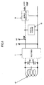
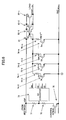
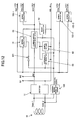
- FIG. 1 is block diagram showing an example of the construction of a related-art power supply circuit.
- the power supply circuit of Fig. 1 includes an antenna 10, a rectifier 11, a digital volume 12, a series regulator 13, a capacitor C, and Zener diodes ZD1 and ZD2.
- Electric power received at the antenna 10 is boosted by the operation of resonance effected by the inductance L of the antenna and the capacitor C connected in parallel, and is then supplied to the rectifier 11 as alternating voltage.
- the magnitude of resonance may become infinite if there is no load.
- the Zener diodes ZD1 and ZD2 are thus provided for the purpose of preventing excessive voltage.
- the rectifier 11 converts the alternating voltage supplied from the antenna 10 into a direct-current voltage.
- the digital volume 12 serves as a pseudo load to adjust the input voltage VDP to a proper voltage level.
- the series regulator 13 attends to voltage control responsive to a load change, thereby supplying a constant direct-current voltage to the load.
- the antenna In the case of making a contact, the antenna is not used, and power is supplied through terminals N1 and N2.
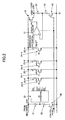
- Fig. 2 is a circuit diagram showing a detailed circuit construction of the digital volume 12 and the series regulator 13 of Fig. 1.
- the digital volume 12 includes resistors 21 and 22, an AD converter 23, transistors 24-0 through 24-m, resistors 25-0 through 25-m having respective resistances R0 through R0/2 m , and a transistor 26.
- the series regulator 13 includes an operational amplifier 31, a transistor 32, resistors 33 and 34, and a transistor 35.
- the resistors 21 and 22 divide a direct-current voltage VDP supplied from the rectifier 11 of Fig. 1.
- the AD converter 23 converts the divided potential into a digital value comprised of D0 through Dm, and controls the ON/OFF of the transistors 24-0 through 24-m according to this digital value.
- the resistors 25-0 through 25-m having respective resistances R0, R0/2, ..., and R0/(2 m ) are selectively coupled to the voltage VDP according to the digital value.
- the adjustment of combined resistance is such that the higher the detected value of the direct-current voltage VDP, the lower the combined resistance is. This achieves control that maintains the voltage VDP at a constant level.
- the series regulator 13 generates a voltage VDDF lower than the voltage VDP in the manner as follows.
- the voltage VDDF is divided by the resistors 33 and 34, and the operational amplifier 31 compares the divided potential with a reference potential.
- the operational amplifier 31 controls the gate voltage to make the transistor 32 more conductive if the divided potential is lower than the reference potential, and controls the gate voltage to make the transistor 32 less conductive if the divided potential is higher than the reference potential.
- Such feedback control by the operational amplifier 31 makes the voltage VDDF constant.
- a control signal when its voltage level is low, turns off the transistor 35, thereby suspending the control function of the operational amplifier 31.
- the control function of the operational amplifier 31 is turned on.
- the related-art regulator circuit shown in Fig. 1 and Fig. 2 has drawbacks as follows.
- the transistor 32 which is controlled by the operational amplifier 31 of the series regulator 13, is connected in series to the load. If an increase in the load causes the output voltage VDDF to drop, the transistor 32 is controlled to be more conductive, thereby increasing a supply current. If a decrease in the load causes the output voltage VDDF to rise, the transistor 32 is controlled to be less conductive, thereby decreasing a supply current. In this construction, the electric current flowing through the transistor 32 is controlled so as to change the electric current running through the load, thereby controlling the voltage. If the response speed of the operational amplifier 31 is increased, a difference of speed between voltage changes and feedback control becomes large. There may thus be a risk of letting the operational amplifier 31 oscillate. Because of this reason, it is difficult to cope with a sudden change in the load by enhancing the response speed of the operational amplifier 31.
- the digital value of the digital volume 12 is set as a given proper value.
- Electric wave received at the antenna 10 not only includes an electric wave for power-supply purposes, but also includes superimposed AM modulated signals for the purpose of communicating information necessary for the IC card. Therefore, the response speed of the digital volume 12 for keeping the voltage VDP constant is set to a sufficiently slow speed that would not absorb the modulated signals.
- the control of the voltage VDDF by the operational amplifier 31 may not be sufficiently fast, resulting in the voltage VDP on the input side being changed. Since the response speed of the digital volume 12 is slow as described above, the voltage VDP is let drop, failing to maintain the constant voltage level.
- the invention provides a power supply circuit for supplying power to a load, the power supply circuit including an antenna which receives electric power, a rectifier coupled to the antenna and configured to convert an alternating voltage supplied from the antenna into a direct-current voltage, a voltage step-down circuit which steps down the direct-current voltage to generate an output voltage for provision to the load, a regulator which controls a resistance connected between the output voltage and a ground voltage in parallel with the load, thereby controlling a voltage level of the output voltage.
- the above-noted resistance may be an on-resistance of a transistor, and the on-resistance of this transistor may be controlled by an operational amplifier operating in response to the output voltage.
- the on-resistance of the transistor is provided in parallel with the load. If an increase in the load causes the output voltage to drop, the transistor is controlled to be less conductive, thereby increasing an electric current supplied to the load. If a decrease in the load causes the output voltage to rise, the transistor is controlled to be more conductive, thereby decreasing an electric current supplied to the load.
- the on-resistance of the transistor connected in parallel with the output voltage and serving as part of the load is changed, thereby controlling the output voltage appearing at one end of the transistor.
- the response speed of the operational amplifier can thus be increased to bring about a commensurate increase in the speed of voltage control.
- the operational amplifier thus does not oscillate.
- the construction of the invention makes it possible to cope with a sudden change in the load by increasing the response speed of the operational amplifier. It is thus possible to provide stable power by keeping the output voltage constant against sudden changes in the load. Since the output voltage does not change, further, it is possible to avoid the fluctuation of an input voltage responding to a change in the load.
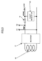
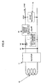
- Fig. 3 is a block diagram showing a first embodiment of a power supply circuit according to the invention.
- the same elements as those of Fig. 1 are referred to by the same numerals, and a description thereof will be omitted.
- the power supply circuit of Fig. 3 includes the antenna 10, the rectifier 11, a voltage step-down circuit 41, and a shunt regulator 42. Although the capacitor C and the Zener diodes ZD1 and ZD2 for the resonance purpose are not illustrated in Fig. 3, these elements may as well be provided as in the construction of Fig. 1.
- Electric power received at the antenna 10 is supplied to the rectifier 11 as an alternating voltage.
- the rectifier 11 converts the alternating voltage supplied from the antenna 10 into a direct-current voltage.
- the voltage step-down circuit 41 steps down the direct-current voltage supplied from the rectifier 11, thereby generating an output voltage VDDF.
- the shunt regulator 42 controls a shunt resistor provided between the output voltage VDDF and the ground GND according to the change of the load so as to maintain the output voltage VDDF at constant voltage.
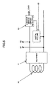
- Fig. 4 is a circuit diagram showing a detailed circuit construction of the voltage step-down circuit 41 and the shunt regulator 42 shown in Fig. 3.
- the voltage step-down circuit 41 includes a resistor 51.
- the shunt regulator 42 includes resistors 52 and 53, an operational amplifier 54, and transistors 55 and 56.
- the resistor 51 serving as the voltage step-down circuit 41 steps down the direct-current voltage VDP supplied from the rectifier 11 of Fig. 3, thereby generating the output voltage VDDF.
- the resistors 52 and 53 of the shunt regulator 42 divide the output voltage VDDF to provide a non-inverted input into the operational amplifier 54.
- An inverted input node of the operational amplifier 54 receives a reference potential.
- the operational amplifier 54 compares the divided potential with the reference potential.
- the operational amplifier 54 controls the gate voltage to make the transistor 55 less conductive if the divided potential is lower than reference potential, and controls the gate voltage to make the transistor 55 more conductive if the divided potential is higher than the reference voltage. With such feedback control by the operational amplifier 54, the voltage VDDF is adjusted to be constant.
- the transistor 55 which controlled by the operational amplifier 54 of the shunt regulator 42 is provided in parallel with the load. If an increase in the load causes the output voltage VDDF to drop, the transistor 55 is controlled to be less conductive, thereby increasing an electric current supplied to the load. If a decrease in the load causes the output voltage VDDF to rise, the transistor 55 is controlled to be more conductive, thereby decreasing an electric current supplied to the load. With this provision, the ON resistance of the transistor 55 connected in parallel with the output voltage VDDF and serving as part of the load is changed, thereby controlling the output voltage VDDF appearing at one end of the transistor 55. If the size of the transistor 55 is sufficiently large, the response speed of the operational amplifier 54 may be increased to bring about a commensurate increase in the speed of voltage control. The operational amplifier 54 thus does not oscillate.
- the construction of the first embodiment of the invention as shown in Fig. 3 and Fig. 4 makes it possible to cope with a sudden change in the load by increasing the response speed of the operational amplifier 54. It is thus possible to provide stable power by keeping the output voltage VDDF constant against sudden changes in the load.
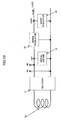
- Fig. 5 is a block diagram showing a second embodiment of the power supply circuit according to the invention.
- the same elements as those of Fig. 1 are referred to by the same numerals, and a description thereof will be omitted.
- the power supply circuit of Fig. 5 includes the antenna 10, the rectifier 11, a current mirror circuit regulator 61, and a digital volume 62.
- the capacitor C and the Zener diodes ZD1 and ZD2 for the resonance purpose are not illustrated in Fig.53, these elements may as well be provided as in the construction of Fig. 1.
- Electric power received at the antenna 10 is supplied to the rectifier 11 as an alternating voltage.
- the rectifier 11 converts the alternating voltage supplied from the antenna 10 into a direct-current voltage.
- the current mirror circuit regulator 61 serves to supply a predetermined amount of an electric current to the load by utilizing the principle of a current mirror circuit.
- the digital volume 62 controls the amount of an electric current supplied from the current mirror circuit regulator 61 to the load so as to achieve a constant current amount, and also adjusts the input voltage VDP to a proper voltage.
- Fig. 6 is a circuit diagram showing a detailed circuit construction of the current mirror circuit regulator 61 and the digital volume 62 of Fig. 5.
- the current mirror circuit regulator 61 includes a transistor 81 and n transistors 82-1 through 82-n.
- a current mirror circuit is constructed by connecting together the gate of the transistor 81 and the gates of the transistors 82-1 through 82-n, so that an equal amount of an electric current flows through each transistor. If the amount of a current running through the transistor 81 is denoted as I, then, an electric current in a total amount of nI flows into the load.
- the digital volume 62 includes resistors 71 and 72, an AD converter 73, transistors 74-0 through 74-m, resistors 75-0 through 75-m having respective resistances R0 through R0/2 m , and a transistor 76.
- the resistors 71 and 72 divide a direct-current voltage VDP supplied from the rectifier 11 of Fig. 5.
- the AD converter 73 converts the divided potential into a digital value comprised of D0 through Dm, and controls the ON/OFF of the transistors 74-0 through 74-m according to this digital value.
- the resistors 75-0 through 75-m having respective resistances R0, R0/2, ..., and R0/(2 m ) are selectively coupled to the gate-drain nodes of the transistor 81 of the current mirror circuit regulator 61 according to the digital value.
- the adjustment of combined resistance is made such that the higher the detected value of the direct-current voltage VDP (i.e., the higher the divided potential detected by the AD converter 73), the lower the combined resistance is. This feedback control makes it possible to keep the voltage VDP constant.
- the use of a current mirror circuit fixes the amount of an electric current supplied to the load to a predetermined amount regardless of changes in the load, and the digital volume 62 controls the input voltage VDP so as to keep it constant. Even when the load exhibits a sudden change, the current mirror circuit functions to keep constant the current supplied to the load, so that the input voltage VDP does not change. Moreover, the provision of the digital volume makes it possible to keep the input voltage VDP constant so as to provide stable power even if the electric power supplied from the antenna fluctuates.
- the digital volume 62 may be replaced by a resistor having a fixed resistance value, such that this resistor connects between the gate-drain nodes of the transistor 81 of the current mirror circuit regulator 61 and the ground potential GND.
- a resistor having a fixed resistance value such that this resistor connects between the gate-drain nodes of the transistor 81 of the current mirror circuit regulator 61 and the ground potential GND.
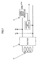
- Fig. 7 is a block diagram showing a variation of the second embodiment of the power supply circuit according to the invention.
- the same elements as those of Fig. 5 are referred to by the same numerals, and a description thereof will be omitted.
- a hardwired-set resistor 65 is provided in place of the digital volume 62 of Fig. 5.
- Fig. 8 is a circuit diagram showing a detailed circuit construction of the current mirror circuit regulator 61 and the hardwired-set resistor 65 of Fig. 7.
- Fig. 8 the same elements as those of Fig. 6 are referred to by the same numerals, and a description thereof will be omitted.
- the hardwired-set resistor 65 includes AND circuits 91-0 through 91-m, transistors 94-0 through 94-m, and resistors 95-0 through 95-m having respective resistances R0 through R0/2 m .
- One input of the AND circuits 91-0 through 91-m receives a respective predetermined setting value, and the other input thereof receives a control signal.
- the control signal is HIGH, the ON/OFF of the transistors 94-0 through 94-m is controlled according to the predetermined setting values.
- the resistors 95-0 through 95-m having respective resistances R0, R0/2, ..., and R0/(2 m ) are selectively coupled to one end of the transistor 81 of the current mirror circuit regulator 61 according to the setting values.
- the setting values described above are predetermined by taking into account the amount of an electric current that is required by the load connected to the power supply circuit. Even when the load exhibits a sudden change, the current mirror circuit functions to keep constant the current supplied to the load, so that the input voltage VDP does not change.
- the use of a current mirror circuit fixes the amount of an electric current supplied to the load to a predetermined amount regardless of changes in the load, and the hardwired-set resistor 65 adjusts the electric current supplied to the load to a desired amount. This makes it possible to keep the input voltage VDP constant so as to provide stable power even if there is a sudden change in the load.
- Fig. 9 is a block diagram showing a third embodiment of the power supply circuit according to the invention.
- the same elements as those of Fig. 1, Fig. 3, Fig. 5, and Fig. 7 are referred to by the same numerals, and a description thereof will be omitted.
- the power supply circuit of Fig. 9 includes the antenna 10, the rectifier 11, the shunt regulator 42, the current mirror circuit regulator 61, and the digital volume 62 (or hardwired-set resistor 65). Although the capacitor C and the Zener diodes ZD1 and ZD2 for the resonance purpose are not illustrated in Fig. 9, these elements may as well be provided as in the construction of Fig. 1.
- electric power received at the antenna 10 is supplied to the rectifier 11 as an alternating voltage.
- the rectifier 11 converts the alternating voltage supplied from the antenna 10 into a direct-current voltage.
- the current mirror circuit regulator 61 serves as a constant-current source and also as a voltage step-down circuit, and steps down the direct-current voltage supplied from the rectifier 11 so as to generate an output voltage VDDF.
- the shunt regulator 42 controls a shunt resistor provided between the output voltage VDDF and the ground GND according to the change of the load so as to maintain the output voltage VDDF at constant voltage.
- the shunt regulator 42 keeps the output voltage VDDF constant in the same manner as in the first embodiment, thereby providing stable electric power. Also in the same manner as in the second embodiment, due to the fixed-current supply function of the current mirror circuit regulator 61, the input voltage VDP does not change in response to a change in the load. Moreover, if the digital volume 62 is provided, feedback control by the digital volume 62 makes it possible to keep the input voltage VDP constant and provide stable electric power even in the presence of fluctuation of electric power supplied from the antenna.
- Fig. 10 is a block diagram showing a fourth embodiment of the power supply circuit according to the invention.
- the same elements as those of Fig. 1 and Fig. 3 are referred to by the same numerals, and a description thereof will be omitted.
- the power supply circuit of Fig. 10 includes the antenna 10, the rectifier 11, the digital volume 12, the series regulator 13, and the shunt regulator 42. Although the capacitor C and the Zener diodes ZD1 and ZD2 for the resonance purpose are not illustrated in Fig. 10, these elements may as well be provided as in the construction of Fig. 1.
- electric power received at the antenna 10 is supplied to the rectifier 11 as an alternating voltage.
- the rectifier 11 converts the alternating voltage supplied from the antenna 10 into a direct-current voltage.
- the digital volume 12 serves as a pseudo load to adjust the input voltage VDP to a proper voltage level.
- the series regulator 13 steps down the direct-current voltage supplied from the rectifier 11 so as to generate an output voltage VDDF, and attends to current control responsive to a load change, thereby supplying a constant direct current to the load.
- the shunt regulator 42 controls a shunt resistor provided between the output voltage VDDF and the ground GND according to a load change so as to maintain the output voltage VDDF at constant voltage.
- the shunt regulator 42 is additionally provided to the related-art construction shown in Fig. 1.
- the operational amplifier 54 that has sufficient response speed in the shunt regulator 42, it is possible to keep the output voltage VDDF constant and provide stable electric power in response to a sudden change in the load.
- Fig. 11 is a block diagram showing a fifth embodiment of the power supply circuit according to the invention.
- Fig. 11 the same elements as those of Fig. 1, Fig. 3, and Fig. 5 are referred to by the same numerals, and a description thereof will be omitted.
- the power supply circuit of Fig. 11 includes the antenna 10, the rectifier 11, the series regulator 13, the shunt regulator 42, the current mirror circuit regulator 61, an antenna signal detection circuit 100, and an inverter 101.
- the capacitor C and the Zener diodes ZD1 and ZD2 for the resonance purpose are not illustrated in Fig. 11, these elements may as well be provided as in the construction of Fig. 1.
- the electric power received at the antenna 10 is supplied to the rectifier 11 as an alternating voltage.
- the rectifier 11 converts the alternating voltage supplied from the antenna 10 into a direct-current voltage.
- the antenna signal detection circuit 100 detects a signal from the antenna 10 to output a detection signal indicative of the presence of noncontact electric power supply.
- the shunt regulator 42 and the current mirror circuit regulator 61 start operation thereof while the series regulator 13 suspends its operation.
- the current mirror circuit regulator 61 serves as a constant-current source and also as a voltage step-down circuit, and steps down the direct-current voltage supplied from the rectifier 11 so as to generate an output voltage VDDF.
- the shunt regulator 42 controls a shunt resistor provided between the output voltage VDDF and the ground GND according to the change of the load so as to maintain the output voltage VDDF at constant voltage. Even if a sudden change in the load occurs, the shunt regulator 42 keeps the output voltage VDDF constant in the same manner as in the first embodiment, thereby providing stable electric power. Also in the same manner as in the second embodiment, due to the fixed-current supply function of the current mirror circuit regulator 61, the input voltage VDP does not change in response to a change in the load.
- the antenna signal detection circuit 100 does not detect a signal from the antenna 10, and thus does not output the detection signal indicative of noncontact electric power supply. Since the detection signal indicative of noncontact electric power supply is not asserted, the shunt regulator 42 and the current mirror circuit regulator 61 are put in the dormant state while the series regulator 13 is put in the operating state.
- the series regulator 13 steps down the direct-current voltage supplied from the contact terminals N1 and N2 so as to generate the output voltage VDDF, and attends to current control responsive to a load change to control the output voltage VDDF to keep it constant.
- the response speed of the series regulator 13 may be so slow that the control of the voltage VDDF does not follow changes in the load. Even in such a case, the voltage VDP does not drop since the input voltage VDP is supplied from the contact terminals N1 and N2.
- an electric current may flow all the time in the current mirror circuit even during a period in which load circuitry is in a suspended state, resulting in an excessive current being consumed.
- the current mirror circuit regulator 61 and the shunt regulator 42 are suspended while the series regulator 13 attends to voltage control. This successfully avoids the consumption of an excessive electric current.
- Fig. 12 is a block diagram showing a sixth embodiment of the power supply circuit according to the invention.
- the same elements as those of Fig. 11, Fig. 5, and Fig. 7 are referred to by the same numerals, and a description thereof will be omitted.
- the power supply circuit of Fig. 12 includes the antenna 10, the rectifier 11, the series regulator 13, the shunt regulator 42, the current mirror circuit regulator 61, the digital volume 62, the hardwired-set resistor 65, the antenna signal detection circuit 100, the inverter 101, and series regulators 102-1 through 102-3.
- the capacitor C and the Zener diodes ZD1 and ZD2 for the resonance purpose are not illustrated in Fig. 12, these elements may as well be provided as in the construction of Fig. 1.
- Fig. 12 The construction of Fig. 12 is the same as the construction of Fig. 11 as far as the basic principle of operation is concerned. That is, the use of the series regulator 13 and the use of the current mirror circuit regulator 61 are switched, depending on whether the case of noncontact electric power supply through the antenna 10 or the case of contact electric power supply through the contact terminals N1 and N2.
- the construction of Fig. 12 is provided with the digital volume 62 and the hardwired-set resistor 65 in addition to the construction of Fig. 11. According to needs, the digital volume 62 may attend to the control of the input voltage VDP, or the hardwired-set resistor 65 may set an electric current for the current mirror circuit regulator 61.
- the series regulators 102-1 through 102-3 have the same construction as the series regulator 13, and may be used to supply different voltages to different load circuits. Moreover, as illustrated in Fig. 12, there may be a path provided to supply the input voltage VDP directly to the load circuitry.
- the input voltage VDP is controlled to be constant regardless of load changes in the case of noncontact electric power supply, and the output voltages VDD1 and VDD2 are controlled to be constant even under the presence of sudden load changes.
- the operation of the current mirror circuit regulator 61 is suspended, thereby avoiding excessive current consumption.
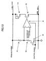
- Fig. 13 is a circuit diagram showing a variation of the shunt regulator used in the invention.
- the same elements as those of Fig. 4 are referred to by the same numerals, and a description thereof will be omitted.
- the shunt regulator of Fig. 13 is provided with a transistor 110 connected in series with the transistor 55 in addition to the construction of the shunt regulator 42 of Fig. 4. With this provision, the range of a gate voltage is narrowed that is used when adjusting the gate voltage of the transistor 55 by the operational amplifier 54. This makes it possible to further increase the speed of voltage adjustment of the shunt regulator.
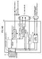
- Figs. 14A and 14B are block diagrams showing the construction of an IC card in which the regulator of the invention is incorporated.
- An IC card 200 shown in Fig. 14A includes the antenna 10, a contact/contactless I/F circuit 201, a memory unit 202, an OS unit 203, an encryption circuit 204, a logic circuit 205, a CPU 206, and a contact terminal 207.
- the antenna 10 is provided for the purpose of receiving electric power and signals through noncontact means.
- the contact terminal 207 is provided for the purpose of receiving electric power and signals through contact means.
- the contact/contactless I/F circuit 201 performs power supply voltage generation, demodulation operation, etc.
- the memory unit 202, the OS unit 203, the encryption circuit 204, the logic circuit 205, and the CPU 206 together form a circuit core unit that performs various processing according to the application in which the IC card is used.
- Fig. 14B shows the construction of the contact/contactless I/F circuit 201.
- the contact/contactless I/F circuit 201 includes the resonance capacitor C, the rectification circuit 11, a regulator 210 according to the invention, a reset circuit 211, a voltage detection circuit 212, a clock extraction circuit 213, a demodulation circuit 214, and a load circuit 215.
- the power supply voltage generated by the regulator 210 is smoothed out by the smoothing capacitor 216 for provision to each circuit portion of the IC card 200.
- signals received by the antenna 10 are supplied to the clock extraction circuit 213, the demodulation circuit 214, etc.
- Signals received by the antenna 10 include not only electric waves for power supply but also AM modulated signals, clock signals, etc., which are superimposed on the electric waves for communication purposes. In order to avoid the loss of modulated signals, therefore, the response speed of the digital volume 12 of Fig. 1 or the like needs to be set to a rather slow speed.
- the regulator 210 according to the invention is configured as was described in connection with the embodiments, so as to prevent the input-side direct-current voltage from fluctuating in response to a sudden change in the load. This makes it possible to supply a stable power supply voltage to each circuit potion of the IC card 200.
Landscapes
- Engineering & Computer Science (AREA)
- Computer Hardware Design (AREA)
- Microelectronics & Electronic Packaging (AREA)
- Theoretical Computer Science (AREA)
- Physics & Mathematics (AREA)
- General Physics & Mathematics (AREA)
- Artificial Intelligence (AREA)
- Computer Vision & Pattern Recognition (AREA)
- Computer Networks & Wireless Communication (AREA)
- General Engineering & Computer Science (AREA)
- Continuous-Control Power Sources That Use Transistors (AREA)
- Control Of Electrical Variables (AREA)
Applications Claiming Priority (2)
| Application Number | Priority Date | Filing Date | Title |
|---|---|---|---|
| JP2004023982 | 2004-01-30 | ||
| JP2004023982A JP4455079B2 (ja) | 2004-01-30 | 2004-01-30 | 電源回路 |
Publications (3)
| Publication Number | Publication Date |
|---|---|
| EP1560147A2 true EP1560147A2 (de) | 2005-08-03 |
| EP1560147A3 EP1560147A3 (de) | 2006-05-24 |
| EP1560147B1 EP1560147B1 (de) | 2013-01-16 |
Family
ID=34650853
Family Applications (1)
| Application Number | Title | Priority Date | Filing Date |
|---|---|---|---|
| EP04017022A Expired - Lifetime EP1560147B1 (de) | 2004-01-30 | 2004-07-19 | Gegen Lastschwankungen stabile Leistungsversorgungsschaltung |
Country Status (4)
| Country | Link |
|---|---|
| US (1) | US7141939B2 (de) |
| EP (1) | EP1560147B1 (de) |
| JP (1) | JP4455079B2 (de) |
| KR (1) | KR100693852B1 (de) |
Cited By (3)
| Publication number | Priority date | Publication date | Assignee | Title |
|---|---|---|---|---|
| WO2010051117A1 (en) * | 2008-10-27 | 2010-05-06 | Atmel Corporation | Contactless interface |
| EP1916532A3 (de) * | 2006-10-27 | 2010-10-06 | Kabushiki Kaisha Toshiba | Erzeugungsvorrichtung für Auslösesignal |
| EP2860667A1 (de) * | 2013-10-08 | 2015-04-15 | ams AG | Spannungsbegrenzer, Funkfrequenzsystem und Verfahren zur Begrenzung einer Spannung |
Families Citing this family (17)
| Publication number | Priority date | Publication date | Assignee | Title |
|---|---|---|---|---|
| KR100659296B1 (ko) | 2005-12-27 | 2006-12-20 | 삼성전자주식회사 | 과전압 제어 리미터 및 이를 갖는 rfid 태그 |
| CN101169834A (zh) * | 2006-10-27 | 2008-04-30 | 株式会社东芝 | 触发信号的发生装置 |
| KR100861842B1 (ko) * | 2006-12-21 | 2008-10-07 | 동부일렉트로닉스 주식회사 | 비접촉 카드의 전원 공급 장치 |
| JP4906093B2 (ja) * | 2006-12-27 | 2012-03-28 | 株式会社半導体エネルギー研究所 | 半導体装置 |
| DE102007004804A1 (de) * | 2007-01-31 | 2008-08-07 | Infineon Technologies Ag | Regelschaltung und Verfahren zum Regeln eines Spannungswertes eines ersten Signals und eines Spannungswertes eines zweiten Signals |
| US7911243B2 (en) * | 2007-04-20 | 2011-03-22 | Texas Instruments Incorporated | Driver with programmable power commensurate with data-rate |
| US7971794B2 (en) * | 2008-02-07 | 2011-07-05 | Infineon Technologies Ag | Actively regulated modulation index for contactless IC devices |
| JP2010021008A (ja) * | 2008-07-10 | 2010-01-28 | Koizumi Lighting Technology Corp | Led照明装置 |
| US8643356B2 (en) * | 2009-10-06 | 2014-02-04 | Infineon Technologies Ag | Voltage regulation and modulation circuit |
| JP5528224B2 (ja) * | 2010-06-16 | 2014-06-25 | ルネサスエレクトロニクス株式会社 | 半導体装置 |
| US8892854B2 (en) * | 2011-04-01 | 2014-11-18 | Honeywell International Inc. | Devices that receive data while not directly powered |
| KR101843433B1 (ko) | 2011-04-04 | 2018-05-15 | 삼성전자주식회사 | 전압 조정 회로, 이를 포함하는 비접촉식 카드, 및 비접촉식 카드 시스템 |
| DE102012202595B3 (de) * | 2012-02-21 | 2013-07-25 | Osram Gmbh | Verfahren zum übertragen einer steuerinformation von einer steuervorrichtung zu einem betriebsgerät für mindestens ein leuchtmittel sowie betriebsgerät für mindestens ein leuchtmittel |
| JP6004836B2 (ja) * | 2012-08-22 | 2016-10-12 | ルネサスエレクトロニクス株式会社 | 電源装置、半導体装置、及びワイヤレス通信装置 |
| US9362744B2 (en) | 2012-09-27 | 2016-06-07 | Electronics And Telecommunications Research Institute | Serial loading constant power supply system |
| KR102068653B1 (ko) | 2013-03-13 | 2020-01-21 | 삼성전자주식회사 | 비접촉 ic 카드의 내부 전압 생성기 및 이를 포함하는 비접촉 ic 카드 |
| JP6964968B2 (ja) * | 2016-09-28 | 2021-11-10 | 新コスモス電機株式会社 | 電気機器および電気機器の信号に重畳するノイズを低減する方法 |
Citations (1)
| Publication number | Priority date | Publication date | Assignee | Title |
|---|---|---|---|---|
| GB2333493A (en) | 1998-01-24 | 1999-07-28 | Plessey Telecomm | A contactless smart card with excess current demand detection |
Family Cites Families (15)
| Publication number | Priority date | Publication date | Assignee | Title |
|---|---|---|---|---|
| US5872429A (en) * | 1995-03-31 | 1999-02-16 | Philips Electronics North America Corporation | Coded communication system and method for controlling an electric lamp |
| JP3761001B2 (ja) * | 1995-11-20 | 2006-03-29 | ソニー株式会社 | 非接触型情報カード及びic |
| JPH10240889A (ja) | 1997-02-27 | 1998-09-11 | Kokusai Electric Co Ltd | 非接触icカード |
| DE19708792A1 (de) * | 1997-03-04 | 1998-09-10 | Tridonic Bauelemente | Verfahren und Vorrichtung zum Erfassen des in einer Gasentladungslampe auftretenden Gleichrichteffekts |
| JP2000041130A (ja) * | 1998-07-21 | 2000-02-08 | Canon Inc | ファクシミリ装置、ファクシミリ設定方法及び記憶媒体 |
| US6515919B1 (en) * | 1998-08-10 | 2003-02-04 | Applied Wireless Identifications Group, Inc. | Radio frequency powered voltage pump for programming EEPROM |
| WO2000041130A1 (de) * | 1999-01-07 | 2000-07-13 | Koninklijke Philips Electronics N.V. | Mobiler datenträger |
| US6659352B1 (en) * | 1999-06-02 | 2003-12-09 | Matsushita Electric Industrial Co., Ltd. | Semiconductor integrated circuit, a contactless information medium having the semiconductor integrated circuit, and a method of driving the semiconductor integrated circuit |
| JP2000348152A (ja) | 1999-06-09 | 2000-12-15 | Hitachi Ltd | 非接触icカード |
| JP2001101364A (ja) * | 1999-10-01 | 2001-04-13 | Fujitsu Ltd | 非接触icカード用lsi |
| JP3719587B2 (ja) | 2000-03-28 | 2005-11-24 | 株式会社日立製作所 | 半導体装置とicカード |
| JP3990100B2 (ja) | 2000-09-26 | 2007-10-10 | 株式会社東芝 | 非接触情報記録媒体 |
| JP3487428B2 (ja) | 2000-10-31 | 2004-01-19 | 松下電器産業株式会社 | 電源回路および非接触icカード |
| JP2002288615A (ja) | 2001-03-28 | 2002-10-04 | Matsushita Electric Ind Co Ltd | 非接触icカード |
| JP2003319574A (ja) | 2002-04-25 | 2003-11-07 | Hitachi Ltd | 半導体集積回路装置および非接触型電子装置 |
-
2004
- 2004-01-30 JP JP2004023982A patent/JP4455079B2/ja not_active Expired - Fee Related
- 2004-07-19 EP EP04017022A patent/EP1560147B1/de not_active Expired - Lifetime
- 2004-07-22 US US10/896,080 patent/US7141939B2/en not_active Expired - Lifetime
- 2004-07-30 KR KR1020040060185A patent/KR100693852B1/ko not_active Expired - Fee Related
Patent Citations (1)
| Publication number | Priority date | Publication date | Assignee | Title |
|---|---|---|---|---|
| GB2333493A (en) | 1998-01-24 | 1999-07-28 | Plessey Telecomm | A contactless smart card with excess current demand detection |
Cited By (7)
| Publication number | Priority date | Publication date | Assignee | Title |
|---|---|---|---|---|
| EP1916532A3 (de) * | 2006-10-27 | 2010-10-06 | Kabushiki Kaisha Toshiba | Erzeugungsvorrichtung für Auslösesignal |
| US7904121B2 (en) | 2006-10-27 | 2011-03-08 | Kabushiki Kaisha Toshiba | Generating device of trigger signal |
| WO2010051117A1 (en) * | 2008-10-27 | 2010-05-06 | Atmel Corporation | Contactless interface |
| US8611119B2 (en) | 2008-10-27 | 2013-12-17 | Inside Contactless S.A. | Contactless interface |
| EP2860667A1 (de) * | 2013-10-08 | 2015-04-15 | ams AG | Spannungsbegrenzer, Funkfrequenzsystem und Verfahren zur Begrenzung einer Spannung |
| WO2015051939A1 (en) * | 2013-10-08 | 2015-04-16 | Ams Ag | Radio frequency system and method for limiting a voltage |
| US9940570B2 (en) | 2013-10-08 | 2018-04-10 | Ams Ag | Radio frequency system and method for limiting a voltage |
Also Published As
| Publication number | Publication date |
|---|---|
| JP4455079B2 (ja) | 2010-04-21 |
| KR100693852B1 (ko) | 2007-03-13 |
| US20050168159A1 (en) | 2005-08-04 |
| EP1560147A3 (de) | 2006-05-24 |
| JP2005216134A (ja) | 2005-08-11 |
| KR20050078178A (ko) | 2005-08-04 |
| US7141939B2 (en) | 2006-11-28 |
| EP1560147B1 (de) | 2013-01-16 |
Similar Documents
| Publication | Publication Date | Title |
|---|---|---|
| EP1560147B1 (de) | Gegen Lastschwankungen stabile Leistungsversorgungsschaltung | |
| US20070246546A1 (en) | Information Processing Terminal, IC Card, Portable Communication Device, Wireless Communication Method, and Program | |
| US8559872B2 (en) | Near field communications (NFC) device power harvesting and power supply selection | |
| US7441711B2 (en) | Semiconductor device and IC card | |
| US8126515B2 (en) | Semiconductor integrated circuit, noncontact/contact electronics device using the same and mobile terminal | |
| US20070155444A1 (en) | Power supply IC having switching regulator and series regulator | |
| EP2340511B1 (de) | Kontaktfreie schnittstelle | |
| US6970690B2 (en) | Data processing apparatus and card-sized data processing device | |
| KR20120113129A (ko) | 전압 조정 회로, 이를 포함하는 비접촉식 카드, 및 비접촉식 카드 시스템 | |
| JP2002150250A (ja) | 非接触icカード用icチップ | |
| JP4309891B2 (ja) | 半導体集積回路装置及びそれを用いた非接触型icカード並びに携帯情報端末 | |
| CN111913552A (zh) | 用于数据存储装置的供电管理 | |
| JP4750530B2 (ja) | 半導体集積回路装置及びそれを用いた非接触電子装置 | |
| JP2005222278A (ja) | 非接触ic媒体用インレットおよび非接触ic媒体ならびにそれを用いた通信システム | |
| JP2006501553A (ja) | 非接触データキャリア | |
| US10432034B2 (en) | On-off apparatus and electronic device | |
| CN100539368C (zh) | 使用单个引线支持ic功率输入和功率控制的电路及方法 |
Legal Events
| Date | Code | Title | Description |
|---|---|---|---|
| PUAI | Public reference made under article 153(3) epc to a published international application that has entered the european phase |
Free format text: ORIGINAL CODE: 0009012 |
|
| AK | Designated contracting states |
Kind code of ref document: A2 Designated state(s): AT BE BG CH CY CZ DE DK EE ES FI FR GB GR HU IE IT LI LU MC NL PL PT RO SE SI SK TR |
|
| AX | Request for extension of the european patent |
Extension state: AL HR LT LV MK |
|
| RIC1 | Information provided on ipc code assigned before grant |
Ipc: G06K 19/07 20060101ALI20060127BHEP Ipc: G06K 7/00 20060101AFI20050428BHEP |
|
| PUAL | Search report despatched |
Free format text: ORIGINAL CODE: 0009013 |
|
| AK | Designated contracting states |
Kind code of ref document: A3 Designated state(s): AT BE BG CH CY CZ DE DK EE ES FI FR GB GR HU IE IT LI LU MC NL PL PT RO SE SI SK TR |
|
| AX | Request for extension of the european patent |
Extension state: AL HR LT LV MK |
|
| 17P | Request for examination filed |
Effective date: 20061110 |
|
| AKX | Designation fees paid |
Designated state(s): DE FR |
|
| RAP1 | Party data changed (applicant data changed or rights of an application transferred) |
Owner name: FUJITSU MICROELECTRONICS LIMITED Owner name: FFC LIMITED |
|
| RAP1 | Party data changed (applicant data changed or rights of an application transferred) |
Owner name: FUJITSU MICROELECTRONICS LIMITED Owner name: FUJITSU ADVANCED ENGINEERING LIMITED |
|
| RAP1 | Party data changed (applicant data changed or rights of an application transferred) |
Owner name: FUJITSU SEMICONDUCTOR LIMITED Owner name: FUJITSU ADVANCED ENGINEERING LIMITED |
|
| 17Q | First examination report despatched |
Effective date: 20110117 |
|
| GRAP | Despatch of communication of intention to grant a patent |
Free format text: ORIGINAL CODE: EPIDOSNIGR1 |
|
| GRAS | Grant fee paid |
Free format text: ORIGINAL CODE: EPIDOSNIGR3 |
|
| GRAA | (expected) grant |
Free format text: ORIGINAL CODE: 0009210 |
|
| AK | Designated contracting states |
Kind code of ref document: B1 Designated state(s): DE FR |
|
| RIN1 | Information on inventor provided before grant (corrected) |
Inventor name: KIKUCHI, TAKESHI Inventor name: YAJIMA, SHINJI Inventor name: FUEKI, SHUNSUKE Inventor name: OKUBO, HIROSHI Inventor name: NAGASAWA, TAKAYUKI Inventor name: TERAMOTO, TOSHIYUKI Inventor name: RADECKI, ANDRZEJ Inventor name: ISOBE, MASAYOSHI |
|
| REG | Reference to a national code |
Ref country code: DE Ref legal event code: R096 Ref document number: 602004040772 Country of ref document: DE Effective date: 20130314 |
|
| PLBE | No opposition filed within time limit |
Free format text: ORIGINAL CODE: 0009261 |
|
| STAA | Information on the status of an ep patent application or granted ep patent |
Free format text: STATUS: NO OPPOSITION FILED WITHIN TIME LIMIT |
|
| 26N | No opposition filed |
Effective date: 20131017 |
|
| REG | Reference to a national code |
Ref country code: DE Ref legal event code: R097 Ref document number: 602004040772 Country of ref document: DE Effective date: 20131017 |
|
| PGFP | Annual fee paid to national office [announced via postgrant information from national office to epo] |
Ref country code: DE Payment date: 20140716 Year of fee payment: 11 |
|
| PGFP | Annual fee paid to national office [announced via postgrant information from national office to epo] |
Ref country code: FR Payment date: 20140708 Year of fee payment: 11 |
|
| REG | Reference to a national code |
Ref country code: DE Ref legal event code: R119 Ref document number: 602004040772 Country of ref document: DE |
|
| PG25 | Lapsed in a contracting state [announced via postgrant information from national office to epo] |
Ref country code: DE Free format text: LAPSE BECAUSE OF NON-PAYMENT OF DUE FEES Effective date: 20160202 |
|
| REG | Reference to a national code |
Ref country code: FR Ref legal event code: ST Effective date: 20160331 |
|
| PG25 | Lapsed in a contracting state [announced via postgrant information from national office to epo] |
Ref country code: FR Free format text: LAPSE BECAUSE OF NON-PAYMENT OF DUE FEES Effective date: 20150731 |