EP1560054A1 - Objektiv mit einem Fokussierungsmechanismus - Google Patents
Objektiv mit einem Fokussierungsmechanismus Download PDFInfo
- Publication number
- EP1560054A1 EP1560054A1 EP05250396A EP05250396A EP1560054A1 EP 1560054 A1 EP1560054 A1 EP 1560054A1 EP 05250396 A EP05250396 A EP 05250396A EP 05250396 A EP05250396 A EP 05250396A EP 1560054 A1 EP1560054 A1 EP 1560054A1
- Authority
- EP
- European Patent Office
- Prior art keywords
- lens
- optical
- projections
- optical unit
- light shielding
- Prior art date
- Legal status (The legal status is an assumption and is not a legal conclusion. Google has not performed a legal analysis and makes no representation as to the accuracy of the status listed.)
- Granted
Links
- 230000003287 optical effect Effects 0.000 title claims abstract description 194
- 238000003384 imaging method Methods 0.000 claims description 46
- 230000004907 flux Effects 0.000 description 14
- 239000000463 material Substances 0.000 description 11
- 239000006185 dispersion Substances 0.000 description 8
- 230000008878 coupling Effects 0.000 description 6
- 238000010168 coupling process Methods 0.000 description 6
- 238000005859 coupling reaction Methods 0.000 description 6
- 238000006243 chemical reaction Methods 0.000 description 5
- 230000000717 retained effect Effects 0.000 description 5
- 230000006835 compression Effects 0.000 description 4
- 238000007906 compression Methods 0.000 description 4
- 230000000694 effects Effects 0.000 description 4
- 239000011347 resin Substances 0.000 description 4
- 229920005989 resin Polymers 0.000 description 4
- 230000000644 propagated effect Effects 0.000 description 3
- 239000000853 adhesive Substances 0.000 description 2
- 230000001070 adhesive effect Effects 0.000 description 2
- 230000005540 biological transmission Effects 0.000 description 2
- 238000001746 injection moulding Methods 0.000 description 2
- 238000000465 moulding Methods 0.000 description 2
- 125000006850 spacer group Chemical group 0.000 description 2
- 239000003990 capacitor Substances 0.000 description 1
- 239000011248 coating agent Substances 0.000 description 1
- 238000000576 coating method Methods 0.000 description 1
- 230000000295 complement effect Effects 0.000 description 1
- 238000009434 installation Methods 0.000 description 1
- 230000013011 mating Effects 0.000 description 1
- 229910044991 metal oxide Inorganic materials 0.000 description 1
- 150000004706 metal oxides Chemical class 0.000 description 1
- 230000002265 prevention Effects 0.000 description 1
- 230000003449 preventive effect Effects 0.000 description 1
- 239000004065 semiconductor Substances 0.000 description 1
Images


Classifications
-
- G—PHYSICS
- G02—OPTICS
- G02B—OPTICAL ELEMENTS, SYSTEMS OR APPARATUS
- G02B13/00—Optical objectives specially designed for the purposes specified below
- G02B13/001—Miniaturised objectives for electronic devices, e.g. portable telephones, webcams, PDAs, small digital cameras
- G02B13/0015—Miniaturised objectives for electronic devices, e.g. portable telephones, webcams, PDAs, small digital cameras characterised by the lens design
- G02B13/002—Miniaturised objectives for electronic devices, e.g. portable telephones, webcams, PDAs, small digital cameras characterised by the lens design having at least one aspherical surface
- G02B13/0035—Miniaturised objectives for electronic devices, e.g. portable telephones, webcams, PDAs, small digital cameras characterised by the lens design having at least one aspherical surface having three lenses
-
- G—PHYSICS
- G02—OPTICS
- G02B—OPTICAL ELEMENTS, SYSTEMS OR APPARATUS
- G02B7/00—Mountings, adjusting means, or light-tight connections, for optical elements
- G02B7/02—Mountings, adjusting means, or light-tight connections, for optical elements for lenses
- G02B7/021—Mountings, adjusting means, or light-tight connections, for optical elements for lenses for more than one lens
-
- G—PHYSICS
- G02—OPTICS
- G02B—OPTICAL ELEMENTS, SYSTEMS OR APPARATUS
- G02B7/00—Mountings, adjusting means, or light-tight connections, for optical elements
- G02B7/02—Mountings, adjusting means, or light-tight connections, for optical elements for lenses
- G02B7/022—Mountings, adjusting means, or light-tight connections, for optical elements for lenses lens and mount having complementary engagement means, e.g. screw/thread
-
- G—PHYSICS
- G03—PHOTOGRAPHY; CINEMATOGRAPHY; ANALOGOUS TECHNIQUES USING WAVES OTHER THAN OPTICAL WAVES; ELECTROGRAPHY; HOLOGRAPHY
- G03B—APPARATUS OR ARRANGEMENTS FOR TAKING PHOTOGRAPHS OR FOR PROJECTING OR VIEWING THEM; APPARATUS OR ARRANGEMENTS EMPLOYING ANALOGOUS TECHNIQUES USING WAVES OTHER THAN OPTICAL WAVES; ACCESSORIES THEREFOR
- G03B9/00—Exposure-making shutters; Diaphragms
- G03B9/02—Diaphragms
Definitions
- This invention relates to an optical unit composed of plural optical members, an imaging device having the optical unit, and a portable terminal equipped with this imaging device.
- solid-state image sensors such as CCD (Charge Coupled Device) type image sensors and CMOS (Complementary Metal-Oxide Semiconductor) type image sensors are used.
- CCD Charge Coupled Device
- CMOS Complementary Metal-Oxide Semiconductor
- an optical unit wherein a supporting part which contacts an image sensor is made of light shielding resin and the lens part is made of translucent resin by injection molding on the supporting part and both parts are solidly integrated, and another one wherein a leg part formed on the lens on the photographed object side is pressed into and fitted with a step on the upper circumference of a leg part formed on the lens on the image plane side and a light shielding supporting member is located around the optical system, and moreover another one wherein, a lens on which pins are formed and another lens on which holes are formed are combined and an aperture plate is interposed as a spacer between the two lenses so as to position in the optical axis direction and in the direction perpendicular to the optical axis.
- Patent Document 1 TOKKAI2002-341218 (Fig. 9)
- Patent Document 2 TOKKAI2002-139662 (Fig. 10)
- the one wherein a supporting part which contacts the image sensor is made of light shielding resin, and the lens part is made of translucent resin while both parts are solidly integrated by injection molding on the supporting part can solve the problem concerning unwanted light.
- an optical unit wherein a leg part formed on the lens on the photographed object side is pressed into and fitted with a step on the upper circumference of a leg part formed on the lens on the image plane side, and a light shielding supporting member is located around the optical system avoids unwanted light entering from outer surface of optical system by means of the supporting member.
- unwanted light other than the light flux of photographing among rays of light entering the plane of incidence of lens arranged on the photographed object side is propagated from the circumference-shaped engagement portion to the leg part formed on the lens on the image plane side, and lowers the image contrast of the photographed object.
- an optical unit wherein a lens in which pins are formed and another lens in which holes are formed are combined and an aperture plate is interposed as a spacer between the two lenses so as to position the two lenses in the optical axis direction and the direction perpendicular to the optical axis also has the drawback that an unstable focal point is caused by dispersion of the distance between the two lenses in the optical axis direction, resulting from dispersion of thickness of the aperture plate placed between the two lenses.
- unwanted light other than the light flux of the photographed object, which is propagated from the circumference-shaped engagement portion to the leg part formed on the lens on the image plane side and which results in lowered image contrast of the photographed object.
- an objective of this invention is to attain an optical unit composed of plural optical members, wherein reduction of contrast of the photographed object image caused by unwanted light does not exist and at low cost, as well as that the focal point is stable without fluctuating, and further, it is also an objective to attain an imaging device equipped with this optical unit and a portable terminal equipped with this imaging device.
- Structure 1 is an optical unit composed of at least two optical members each having an optical effective surface and a retaining portion on at least a part of the circumference of the optical effective surface, and a light shielding member having an aperture and provided between the two optical members, wherein at least one optical member of the two optical members has at least three projections formed on the retaining portion of at least one surface thereof and the three projections are brought in contact with the other optical member to form a space in which a part of the light shielding member is interposed at the retaining portions of the two optical members excluding the projections.
- Structure 2 is the optical unit of Structure 1), wherein the projections are brought in contact with the other optical member so as to fix positions of the two optical members in two positional directions of the optical axis direction and the direction perpendicular to the optical axis.
- Structure 3) is the optical unit of Structure 1) or 2), wherein the outer diameter of the light shielding member is made equal to or larger than that of at least one optical member of the two optical members facing the light shielding member.
- Structure 4) is an optical unit of any one of Structures 1) - 3), wherein the aperture of the light shielding member is formed to be substantially rectangular.
- Structure 5) is the optical unit of any one of Structures 1) - 4), wherein the optical unit has at least first, second and third optical members, and the first set of at least three projections provided on the retaining portion between the first and second optical members and the second set of at least three projections provided on the retaining portion between the second and third optical members, and wherein positions of the first set of at least three projections are different from positions of the second set of at least three projections projected on the same circle.
- Structure 6) is an imaging device having the optical unit of any one of Structures 1) - 5).
- Structure 7) is a portable terminal having the imaging device of Structure 6).
- the optical unit of the invention composed of at least two optical members each having an optical effective surface and a retaining portion on at least part of the circumference of the optical effective surface and a light shielding member with an aperture which is placed between the optical members, wherein at least one of the optical members has at least three projections which contact the other optical member on portions other than the optical effective surfaces of at least one surface and a part of the light shielding member is interposed at a portion other than the optical effective surface of the optical member excluding the projections, it is possible to obtain an optical unit composed of plural optical members, wherein reduction of contrast of the photographed object image caused by unwanted light is eliminated and the cost is low, as well as featuring a focal point which is stable.
- the projections contact the other optical member in both the optical axis direction and the direction perpendicular to the optical axis to position the optical members so that it becomes possible to position in the optical axis direction and the direction perpendicular to the optical axis with simple structure and without any other parts, and it becomes possible to obtain optical unit which is featuring a stable focal point, at low cost.
- the diameter of the light shielding member is at least as large as either one of the two optical members facing the light shielding member, to prevent unwanted light passing through optical member, other than the optical effective surface from traveling to the optical member on the image plane side.
- said aperture prefferably to be substantially rectangular, and thereby, only a light flux necessary for photographing can be conducted to the imaging plane side and the image contrast of a photographed object can be further improved.
- the optical unit has at least three optical members and each portion, other than the optical effective surface, of at least two surfaces among the surfaces of the optical members constituting the optical unit has projections, wherein the projections on one surface and the projections on the other surface are located at positions which differ from each other in terms of phase in the circumferential direction, and thereby, unwanted light passing through the projections can also be shielded.
- Fig. 1 is a view of appearance of portable telephone T as an example of a portable terminal equipped with an imaging device related to this invention.
- Portable telephone T shown in Fig. 1, is composed of upper casing 71 as a casing equipped with display screen D and lower casing 72 which is equipped with input buttons P, which are connected through hinge 73.
- Imaging device S is housed at the lower end of the display screen D in upper casing 71 and is positioned so that it can gather light from the'photographed object via an opening through the outer surface of upper casing 71.
- manual manipulation member 75 is located at the lower end of display screen D of upper casing 71.
- This imaging device S may also be positioned at the upper end of display screen D on upper casing 71. Further, the portable telephone is not limited to a folding type.
- Fig. 2 is a perspective view of imaging device 100 equipped with an optical unit related to this invention. This imaging device 100 is installed at the position of imaging device S, as shown in Fig. 1.
- the outer portion of imaging device 100 is composed of printed circuit board 11 on which an image sensor is mounted, connector 17 for connection to other boards in the portable terminal, base member 12, translucent dust-proof plate 21, cap member 13, decorative plate 14 and rotary member 15 on which manipulation part 15S is formed.
- Manipulation part 15S is mechanically connected internally to manual manipulation member 75 shown in Fig.1 so that rotary member 15 is rotated via linkage to manual manipulation member 75.
- Fig. 3 is a general cross-sectional view showing the internal structure of imaging device 100 equipped with the optical unit related to this invention. This figure shows a cross-sectional view taken on line G-G shown in Fig. 2. In the figures to be shown later, like identifying symbols are given to like functional parts to avoid overlap of explanation.
- optical unit 50 composed of No. 1 lens 1, No. 2 lens 2, No. 3 lens 3, aperture plate 4 positioned between No. 1 lens 1 and No. 2 lens 2, aperture plate 5 positioned between No.2 lens 2 and No. 3 lens 3 and aperture plates fixed to the photographed object side of No. 1 lens 1 and the image plane side of No. 3 lens 3, and cam member 7 on which cam parts 7c are formed in the positions corresponding to those of three convexes 3d which are formed as one piece on a portion other than the optical effective surface on the image plane side of No. 3 lens 3, and image sensor 8 installed on printed circuit board 11.
- optical unit 50 which is unitized as one piece, flange part of No.3 lens 3 is urged by compression coil spring 9 toward image sensor 8. Thereby, optical unit 50 is positioned so that the distance to image sensor 8 through cam member 7 is set in the optical axis direction.
- Cam member 7 is made of a translucent material and has translucent portion 7a for light flux from the photographed object, which is formed so as to cover the photoelectric conversion surface side of the image sensor and an infrared shield coating is applied to one surface of translucent portion 7a.
- plural legs 7d are integrally formed on cam member 7 and contact an area other than the photoelectric conversion surface on the photoelectric conversion surface side of image sensor 8.
- Cam member 7 is fitted in the inside of the base member 12 and bonded with adhesives to be retained.
- Base member 12 is engaged with outer frame member 16 which encloses optical unit 50.
- rotary member 15 is mounted rotatably. This rotary member 15 is so mounted that coupling part 15t, which is integrally formed as an inner part of the rotary member, is coupled to coupling part 3k of No.3 lens 3.
- Cap member 13 is mounted on outer frame member 16 after installation of compression coil spring 9.
- An aperture is equipped on side surface of outer frame member 16 and serves as a space in which coupling part 15t formed on the rotary member 15 can be rotated.
- imaging device 100 equipped with optical unit 50 related to this invention is a general description for the internal structure of imaging device 100 equipped with optical unit 50 related to this invention.
- optical unit 50 related to this invention will be explained in detail.
- a surface formed for imaging is designated as an optical effective surface and the surrounding part which does not contribute to imaging is designated as a flange part (retaining part).
- a light shielding member having a aperture corresponds to aperture plates 4 and 5.
- Fig. 4 is an exploded perspective view showing the structures of No. 1 lens 1, No. 2 lens 2 and aperture plate 4 located between the No.1 lens 1 and the No. 2 lens 2.
- the views of No. 1 lens 1 and aperture plate 4 in the figure are perspective ones viewed from the image plane side while the view of No. 2 lens 2 is a perspective one viewed from the photographed object side.
- No. 1 lens 1 is composed so that optical effective surface 1r and flange part 1f formed on the periphery of the optical effective surface are integrally formed of a translucent material
- No. 2 lens 2 is composed so that optical effective surface 2r, flange part 2f, formed on the periphery of the optical effective surface, and four projections 2t on flange part 2f, namely, the projections protruded from the portion other than the optical effective surface are integrally formed of translucent materials.
- the number of the projections is four as shown in Fig. 4, it is preferable that these projections are placed at intervals of about 90 degrees.
- aperture plate 4 has aperture 4k through which light flux from the photographed object passes for photographing and four cutouts 4n in the circumferential positions corresponding to projections 2t of No. 2 lens 2, and aperture plate 4 is made of a light shielding material.
- Arc part 4f of aperture plate 4 representing a light shielding member is made so that its diameter is the same as or bigger than the outer diameter of No. 1 lens 1 as shown in Fig. 3.
- This No. 1 lens 1, No. 2 lens 2 and aperture plate 4 representing a light shielding member are assembled as follows.
- No. 1 lens 1 and No. 2 lens 2 are positioned accurately both in the optical axis direction and in the direction perpendicular to the optical axis without reference to the thickness of aperture plate 4 located between the lenses, by mating contact between side faces 2s as well as top faces 2p on projections 2t of No. 2 lens 2 and side face 1s as well as outer face 1p on flange 1f of No. 1 lens 1.
- Arc parts 4f formed on areas other than the cutouts 4n on aperture plate 4 representing a light shielding member are interposed to lie between the areas other than the optical effective surfaces of No. 1 lens 1 and No. 2 lens 2.
- unwanted light other than a photographing light flux can be prevented from traveling through areas other than the optical effective surfaces of No. 1 lens 1 and No. 2 lens 2 facing each other, and by forming the outer diameter of arc parts of 4f of aperture plate 4 representing a light shielding member to be the same as or larger than the diameter of No.1 lens 1, it is possible to efficiently prevent unwanted light passing through any portion, other than the optical effective surface, from traveling into No. 2 lens 2 which is an optical member on the image plane side.
- Fig. 5 is an exploded perspective view showing the structure of No. 2 lens 2, No. 3 lens 3 and aperture plate 5 which is located between No. 2 lens 2 and No. 3 lens 3.
- No. 2 lens 2 shown in Fig. 5 is the partial perspective view viewed from the image plane side while aperture plate 5 and No. 3 lens 3 show the perspective views viewed from the photographed object side.
- No. 3 lens 3 is structured so that optical effective surface 3r, flange 3f formed on the circumference of 3r, four projections 3t protruding inward from the flange 3f, and coupling part 3k mentioned above are integrally formed of a translucent material.
- the number of the projections is four as shown in Fig. 5, it is preferable that these projections are placed at intervals of about 90 degrees.
- aperture plate 5 has aperture 5k through which light flux from the photographed object passes for photography and four cutouts 5n in the circumferential positions corresponding to projections 3t of No. 3 lens 3.
- No. 2 lens 2, No. 3 lens 3 and aperture plate 5 are assembled as follows.
- Aperture plate 5 is structured to be retained between No. 2 lens 2 and No.3 lens 3 with a small clearance.
- No. 2 lens 2 and No. 3 lens 3 are positioned accurately both in the optical axis direction and in the direction perpendicular to the optical axis without reference to the thickness of aperture plate 5 located between the lenses, by respective contact between side face 3s as well as top face 3p on projections 3t of No. 3 lens 3 and side face 2q as well as outer face 2j on flange 2h of No. 2 lens 2.
- arc parts 5f formed on areas other than the cutouts 5n on aperture plate 5 representing a light shielding member are interposed to lie between the areas other than the optical effective surfaces of No. 2 lens 2 and No. 3 lens 3.
- unwanted light other than a photographing light flux can be prevented from traveling through areas other than the optical effective surfaces of No. 2 lens 2 and No. 3 lens 3 facing each other.
- the diameter of arc part 5f of aperture plate 5 representing a light shielding member to be equal to or larger than the outer diameter of No. 2 lens 2, the effect of preventing traveling of unwanted light other than photographing light flux can be improved.
- No. 1 lens 1, No. 2 lens 2 and No.3 lens 3 are connected with each other so that projections 2t and 3t formed on the portion other than the optical effective surface contact portions, other than the optical effective surface on the other lenses, and are assembled as a unit by bonding each other with adhesives without influence from the aperture plate interposed between lenses, therefore it is possible to minimize deviation of distance between the lenses in the optical axis direction and the direction perpendicular to the optical axis and to obtain an optical unit composed of plural optical members, wherein there is not individual dispersion of focal point or reduction of contrast of photographed object image does not exist because of prevention of unwanted light transmission.
- a low cost optical unit can be obtained without increase of parts or countermeasures by means of insert moldings, because of preventive measures against unwanted light, taken with an aperture plate representing a light shielding member located between the lenses.
- Fig. 6 shows a cross-sectional view of optical unit 50 related to this invention.
- arc part 5f of aperture plate 5 is located between No 2 lens 2 and No. 3 lens 3 to prevent transmission of unwanted light coming from No. 1 lens 1 to No. 3 lens 3 via contacting parts 2t.
- arc part 4f of aperture plate 4 is located between No 1 lens 1 and No. 2 lens 2.
- No. 2 lens 2 and No. 3 lens 3 as an optical unit so that projections 2t of No. 2 lens 2 and projections 3t of No. 3 lens 3 are located out of phase with each other in circumferential direction, and thereby, unwanted light coming through projections 2t of No. 2 lens 2 is prevented from traveling into No. 3 lens 3 via arc parts 5f (refer to Fig. 5) of aperture plate 5.
- Fig. 7 is a perspective view of optical unit 50 integrated as a unit. The figure is the one wherein the optical unit 50 is viewed from a lower point obliquely on the image sensor side.
- three convexes 3d are formed at the positions corresponding to those of cam parts 7c of cam member 7 described in Fig. 3, on portions other than the optical effective surface on the image sensor side.
- Fig. 8 is a perspective view of cam member 7.
- the figure shows cam member 7 viewed from the upper point obliquely on the photographed object side.
- This cam member 7 is made so that translucent part 7a is formed of translucent materials, covering the top face of image sensor 8.
- convex 7h is formed and cam member 7 is positioned in the circumferential direction by fitting this convex 7h into a concave, which is not shown, on base member 12 shown in Fig. 3.
- Gate 7q formed in the place 180 degrees away from convex 7h is formed to be smaller in width and shorter in projecting length than convex 7h and is engaged with another concave, which is not shown, on base member 12.
- Side surface 7f on the outer circumference fits into an inner surface of base member 12, shown in Fig. 3.
- Cam member 7 has cam parts 7c arranged at intervals of 120 degrees close to the outer circumference of cam member 7. Each of these cam parts 7c features high horizontal surface 7m, low horizontal surface 7n and inclined surfaces 7j connecting horizontal surfaces 7m and 7c, which are all different from each other in terms of position in the optical axis direction.
- Three convexes 3d shown in Fig. 7 contact three cam parts 7c on cam member 7 shown in Fig. 8, and when they move from low horizontal surface 7n to high horizontal surface 7m via inclined surface 7j, the position (for example hyperfocal position) where a long distance is in focus is changed to the position for close-up photography, and when they move from high horizontal surface 7m to low horizontal surface 7n through inclined surface 7j the position for close-up photography is changed back to the position where the long distance is in focus.
- the position for example hyperfocal position
- Fig. 9 shows both the position for the close-up photography and the position where the long distance is in focus for optical unit 50 mounted in imaging apparatus 100.
- how the long distance is in focus is shown on the right side of the optical axis "O"
- the condition for close-up photography is shown on the left side.
- convexes 3d contact low horizontal surfaces 7n to obtain the long distance focal point position, and as shown on the left side of the figure, convexes 3d contact high horizontal surfaces 7m to shift optical unit 50 toward the photographed object by prescribed distance to obtain the close-up photographing position.
- No.2 lens and No.3 lens having projections respectively Although the example of No.2 lens and No.3 lens having projections respectively was used in the explanation, it is naturally possible to structure the unit to have projections on both the photographed object side and the image plane side of No. 2 lens to contact No.1 lens and No. 3 lens respectively, or to structure the unit to have projections on No. 1 lens and No.3 lens to contact No.2 lens respectively.
- Fig. 10 is a schematic cross-sectional view of an internal structure of another example of imaging device 100 equipped with an optical unit relating to this invention.
- the imaging device 100 illustrated in Fig. 10 shows an example where this invention is employed for a fixed-focus type device.
- manual manipulation member 75 is not necessary when the device is installed in a portable telephone shown in Fig. 1.
- optical unit 50 is solidly composed of No.1 lens 1, No.2 lens 2, No.3 lens 3, aperture plate 4 positioned between No.1 lens 1 and No.2 lens 2, aperture plate 5 positioned between No.2 lens 2 and No.3 lens 3 and an aperture plate fixed on photographed object side of No. 1 lens 1, wherein leg parts 3g are integrally formed at plural positions on image plane side surface other than optical effective surface of No. 3 lens, and the leg parts 3g contact surfaces other than a photoelectric conversion surface of the photoelectric conversion surface side on image sensor 8.
- the light shielding member with an opening portion corresponds to aperture plate 5.
- optical unit 50 which is unitized as one piece, a flange part of No.2 lens 2 is urged by compression coil spring 9 representing an urging member toward image sensor 8. Thereby, a distance between optical unit 50 and image sensor 8 in the optical axis direction is determined.
- Outer frame member 16 containing optical unit 50 is fixed on printed circuit board 11 and infrared shielding filter 22 is mounted on cap member 13.
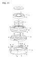
- Fig. 11 is an exploded perspective view showing the structure of No. 1 lens 1, No. 2 lens 2, No. 3 lens 3, an aperture plate 4 located between No. 1 lens 1 and No. 2 lens 2, and an aperture plate 5 located between No. 2 lens 2 and No. 3 lens 3.
- No. 1 lens 1 is composed so that optical effective surface 1r and flange part 1f formed on the periphery of the optical effective surface 1r are integrally formed of a translucent material
- No. 2 lens 2 is composed so that optical effective surface 2r and flange part 2f formed on the periphery of the optical effective surface 2r are integrally formed of a translucent material.
- No. 1 lens 1, No. 2 lens 2 and aperture plate 4 representing a light shielding member are assembled as follows.
- No. 1 lens 1 and No. 2 lens 2 are assembled, with the outer periphery of flange part If of No. 1 lens 1 being in contact with inner wall of flange part 2s of No.2 lens 2 (hatched portion in Fig. 11) and with the lower surface of flange part If of No. 1 lens 1 being in contact with step part 2p formed on inner wall of flange part 2s of no.2 lens 2.
- Aperture plate 4 is inserted between No. 1 lens 1 and No.2 lens 2, and is formed to be retained to maintain a small clearance. Thereby, No. 1 lens 1 and No. 2 lens 2 are positioned accurately through mutual contact, both in the optical axis direction and in the direction perpendicular to the optical axis, without being interfered by aperture plate 4 located between these lenses.
- No. 3 lens 3 is structured so that optical effective surface 3r, flange part 3f formed on the outer circumference of 3r and four projections 3t formed on the flange part 3f are integrally formed of a translucent material.
- aperture plate 5 has aperture 5k formed to be substantially rectangular through which a light flux from the object to be photographed passes for photographing and has four cutouts 5n in the circumferential positions corresponding to projections 3t of No. 3 lens 3 and is made of a light shielding material as shown in Fig. 11.
- No. 3 lens 3 and aperture plate 5 are assembled as follows.
- No. 2 lens 2 and No. 3 lens 3 are assembled, with four projections 3t formed on No.3 lens 3 protruding toward No. 2 lens 2 through cutouts 5n formed on aperture plate 5, with side faces 3s (hatched part in Fig. 11) on projections 3t being in contact with side face 2q (hatched part in Fig 11) formed below flange part 2f of No. 2 lens 2, and with top faces 3p of projections 3t being in contact with lower face 2j on flange 2f of No. 2 lens 2.
- Aperture plate 5 is structured to be retained between No. 2 lens 2 and No.3 lens 3 to maintain a small clearance.
- No. 2 lens 2 and No. 3 lens 3 are positioned accurately both in the optical axis direction and in the direction perpendicular to the optical axis, without being interfered by the thickness of aperture plate 5 representing a light shielding member which has aperture 5k formed to be substantially rectangular and is located between these lenses.
- arc parts 5f formed on areas other than the cutouts 5n on aperture plate 5 are interposed to lie between the areas other than the optical effective surfaces of No. 2 lens 2 and No. 3 lens 3. Thereby, unwanted light other than a photographing light flux can be prevented from traveling through areas other than the optical effective surfaces of No. 2 lens 2 and No. 3 lens 3 facing each other. Further, by forming the diameter of arc part 5f of aperture plate 5 representing a light shielding member, to be equal to or larger than the outer diameter of No. 2 lens 2, the effect of preventing traveling of unwanted light other than a photographing light flux can be improved.
- No.1 lens 1, No. 2 lens 2 and aperture plate 4 can be structured in the same way as in Fig 4.
- a low cost optical unit composed of plural lenses which is stable without dispersion of focal point and is free from contrast loss of the photographed object image, because a distance between lenses is not affected by the thickness of a aperture plate and unwanted light traveling through portions other than the optical effective surface is shielded, by means of forming at least three projections, which contact other lenses, on the portions other than the optical effective surface of at least one lens, and by means of composing an optical unit so that a part of the aperture plate representing a light shielding member may be inserted into the portions other than the optical effective surface, excluding projections.
- optical unit composed of lenses and aperture plates was used in the aforementioned explanation, however, this invention is also applicable to an optical unit having optical members with a flat optical effective surface such as filters, and it does not depart from the invention.
Landscapes
- Physics & Mathematics (AREA)
- General Physics & Mathematics (AREA)
- Optics & Photonics (AREA)
- Lens Barrels (AREA)
- Studio Devices (AREA)
Applications Claiming Priority (2)
| Application Number | Priority Date | Filing Date | Title |
|---|---|---|---|
| JP2004022726 | 2004-01-30 | ||
| JP2004022726 | 2004-01-30 |
Publications (2)
| Publication Number | Publication Date |
|---|---|
| EP1560054A1 true EP1560054A1 (de) | 2005-08-03 |
| EP1560054B1 EP1560054B1 (de) | 2008-09-17 |
Family
ID=34650837
Family Applications (1)
| Application Number | Title | Priority Date | Filing Date |
|---|---|---|---|
| EP05250396A Expired - Lifetime EP1560054B1 (de) | 2004-01-30 | 2005-01-26 | Objektiv mit einem Fokussierungsmechanismus |
Country Status (4)
| Country | Link |
|---|---|
| EP (1) | EP1560054B1 (de) |
| KR (1) | KR101092198B1 (de) |
| DE (1) | DE602005009756D1 (de) |
| TW (1) | TW200527881A (de) |
Cited By (8)
| Publication number | Priority date | Publication date | Assignee | Title |
|---|---|---|---|---|
| EP1887397A4 (de) * | 2006-04-13 | 2009-03-11 | Milestone Co Ltd | Gerät zum vorschub einer abbildungslinse und methode zum zusammenbau |
| US10412288B2 (en) | 2014-05-16 | 2019-09-10 | Sharp Kabushiki Kaisha | Camera module including image sensor and camera window holding mechanism |
| EP3575844A4 (de) * | 2017-01-26 | 2021-01-13 | Ningbo Sunny Opotech Co., Ltd. | Linse, kameramodul und herstellungsverfahren dafür |
| CN112433419A (zh) * | 2017-02-24 | 2021-03-02 | 大立光电股份有限公司 | 遮光片、光学镜片组、成像镜头与电子装置 |
| WO2021120158A1 (zh) * | 2019-12-20 | 2021-06-24 | 诚瑞光学(常州)股份有限公司 | 镜头结构 |
| EP3783412A4 (de) * | 2018-06-14 | 2021-07-28 | Guangdong Oppo Mobile Telecommunications Corp., Ltd. | Bildgebungsmodul, kameraanordnung und elektronische vorrichtung |
| CN113992835A (zh) * | 2021-12-27 | 2022-01-28 | 江西联益光学有限公司 | 摄像头模组及其组装方法和电子模块 |
| DE102021117233B4 (de) * | 2020-07-21 | 2026-02-12 | Ifm Electronic Gmbh | Schutzvorrichtung zur Stabilitätserhöhung eines optischen Gehäuseelements sowie eine Verwendung der Schutzvorrichtung und einen Satz mit der Schutzvorrichtung |
Families Citing this family (3)
| Publication number | Priority date | Publication date | Assignee | Title |
|---|---|---|---|---|
| CN103852851A (zh) * | 2012-12-06 | 2014-06-11 | 玉晶光电(厦门)有限公司 | 可消除杂散光线的成像镜头 |
| KR20170129588A (ko) * | 2016-05-17 | 2017-11-27 | 마이크로엑츄에이터(주) | 렌즈 모듈 및 이를 구비한 카메라 렌즈 조립체 |
| JP2019082623A (ja) * | 2017-10-31 | 2019-05-30 | 日本電産三協電子(東莞)有限公司 | 光学ユニット |
Citations (4)
| Publication number | Priority date | Publication date | Assignee | Title |
|---|---|---|---|---|
| US5612826A (en) * | 1994-07-25 | 1997-03-18 | Nikon Corporation | Lens holding device for holding a lens system and method for making |
| EP1174748A2 (de) * | 2000-07-17 | 2002-01-23 | Kabushiki Kaisha Toshiba | Optische Objektivmasseinheit, die eine Vorrichtung für die Anpassung des Schwerpunktes des Objektivs hat |
| JP2002118776A (ja) * | 2000-10-10 | 2002-04-19 | Konica Corp | 撮像装置 |
| JP2003037758A (ja) * | 2001-01-12 | 2003-02-07 | Konica Corp | 撮像装置 |
Family Cites Families (3)
| Publication number | Priority date | Publication date | Assignee | Title |
|---|---|---|---|---|
| JP2002139662A (ja) | 2000-11-06 | 2002-05-17 | Konica Corp | 撮像装置 |
| JP2002182090A (ja) | 2000-12-18 | 2002-06-26 | Ricoh Co Ltd | リブ一体型レンズ、これを用いた光学ユニット、画像読取装置および画像形成装置 |
| JP2004004742A (ja) * | 2002-04-16 | 2004-01-08 | Konica Minolta Holdings Inc | 小型の撮像レンズ、撮像ユニット及び携帯端末 |
-
2005
- 2005-01-25 TW TW094102174A patent/TW200527881A/zh unknown
- 2005-01-26 EP EP05250396A patent/EP1560054B1/de not_active Expired - Lifetime
- 2005-01-26 DE DE602005009756T patent/DE602005009756D1/de not_active Expired - Lifetime
- 2005-01-27 KR KR1020050007345A patent/KR101092198B1/ko not_active Expired - Lifetime
Patent Citations (4)
| Publication number | Priority date | Publication date | Assignee | Title |
|---|---|---|---|---|
| US5612826A (en) * | 1994-07-25 | 1997-03-18 | Nikon Corporation | Lens holding device for holding a lens system and method for making |
| EP1174748A2 (de) * | 2000-07-17 | 2002-01-23 | Kabushiki Kaisha Toshiba | Optische Objektivmasseinheit, die eine Vorrichtung für die Anpassung des Schwerpunktes des Objektivs hat |
| JP2002118776A (ja) * | 2000-10-10 | 2002-04-19 | Konica Corp | 撮像装置 |
| JP2003037758A (ja) * | 2001-01-12 | 2003-02-07 | Konica Corp | 撮像装置 |
Non-Patent Citations (2)
| Title |
|---|
| PATENT ABSTRACTS OF JAPAN vol. 2002, no. 08 5 August 2002 (2002-08-05) * |
| PATENT ABSTRACTS OF JAPAN vol. 2003, no. 06 3 June 2003 (2003-06-03) * |
Cited By (12)
| Publication number | Priority date | Publication date | Assignee | Title |
|---|---|---|---|---|
| EP1887397A4 (de) * | 2006-04-13 | 2009-03-11 | Milestone Co Ltd | Gerät zum vorschub einer abbildungslinse und methode zum zusammenbau |
| US7616388B2 (en) | 2006-04-13 | 2009-11-10 | Milestone Co., Ltd. | Image capture lens feeding device and method of assembly of same |
| US10412288B2 (en) | 2014-05-16 | 2019-09-10 | Sharp Kabushiki Kaisha | Camera module including image sensor and camera window holding mechanism |
| EP3575844A4 (de) * | 2017-01-26 | 2021-01-13 | Ningbo Sunny Opotech Co., Ltd. | Linse, kameramodul und herstellungsverfahren dafür |
| US11579341B2 (en) | 2017-01-26 | 2023-02-14 | Ningbo Sunny Opotech Co., Ltd. | Lens, camera module and manufacturing method thereof |
| US12007583B2 (en) | 2017-01-26 | 2024-06-11 | Ningbo Sunny Opotech Co., Ltd. | Lens, camera module and manufacturing method thereof |
| CN112433419A (zh) * | 2017-02-24 | 2021-03-02 | 大立光电股份有限公司 | 遮光片、光学镜片组、成像镜头与电子装置 |
| EP3783412A4 (de) * | 2018-06-14 | 2021-07-28 | Guangdong Oppo Mobile Telecommunications Corp., Ltd. | Bildgebungsmodul, kameraanordnung und elektronische vorrichtung |
| US11503193B2 (en) | 2018-06-14 | 2022-11-15 | Guangdong Oppo Mobile Telecommunications Corp., Ltd. | Imaging module, camera assembly and electronic device |
| WO2021120158A1 (zh) * | 2019-12-20 | 2021-06-24 | 诚瑞光学(常州)股份有限公司 | 镜头结构 |
| DE102021117233B4 (de) * | 2020-07-21 | 2026-02-12 | Ifm Electronic Gmbh | Schutzvorrichtung zur Stabilitätserhöhung eines optischen Gehäuseelements sowie eine Verwendung der Schutzvorrichtung und einen Satz mit der Schutzvorrichtung |
| CN113992835A (zh) * | 2021-12-27 | 2022-01-28 | 江西联益光学有限公司 | 摄像头模组及其组装方法和电子模块 |
Also Published As
| Publication number | Publication date |
|---|---|
| EP1560054B1 (de) | 2008-09-17 |
| TW200527881A (en) | 2005-08-16 |
| DE602005009756D1 (de) | 2008-10-30 |
| KR20050078209A (ko) | 2005-08-04 |
| KR101092198B1 (ko) | 2011-12-13 |
Similar Documents
| Publication | Publication Date | Title |
|---|---|---|
| JP6434549B2 (ja) | フィルターアセンブリ及びこれを具えるカメラモジュール | |
| KR101092124B1 (ko) | 촬상 장치, 상기 촬상 장치를 구비한 휴대 단말 및 촬상장치의 제조 방법 | |
| TW578422B (en) | Image pick-up apparatus and portable telephone utilizing the same | |
| CN100405111C (zh) | 照相机镜头模块 | |
| KR20080056619A (ko) | 카메라 모듈 | |
| EP1560054B1 (de) | Objektiv mit einem Fokussierungsmechanismus | |
| CN101518050A (zh) | 固态摄像装置及其制作方法 | |
| KR100816143B1 (ko) | 촬상 장치 및 이를 구비한 휴대 단말 및 촬상 장치의 조립방법 | |
| JP2002118776A (ja) | 撮像装置 | |
| JP4691674B2 (ja) | 光学ユニット及び撮像装置並びに携帯端末 | |
| JP2004254259A (ja) | 撮像装置及び小型電子機器 | |
| TW200425493A (en) | Image pickup device and portable terminal | |
| CN102854549B (zh) | 晶片级透镜模块、晶片级多镜头感光模块及其制作方法 | |
| JP4492085B2 (ja) | 撮像装置及び携帯端末 | |
| KR101036365B1 (ko) | 카메라 모듈 | |
| JP4517623B2 (ja) | 撮像装置及び該撮像装置を備えた携帯端末 | |
| EP1531617A1 (de) | Bildaufnahmevorrichtung und tragbares Endgerät mit einer Bildaufnahmevorrichtung | |
| JP4403770B2 (ja) | 撮像装置及び撮像装置の製造方法 | |
| JP2005045755A (ja) | 撮像装置及び該撮像装置を備えた携帯端末 | |
| JP2005257850A (ja) | 光学ユニット及び該光学ユニットを備えた撮像装置並びに該撮像装置を備えた携帯端末 | |
| JP2006217186A (ja) | 薄型デジタルカメラ及びデジタルカメラの撮像機構 | |
| JP4873375B2 (ja) | 撮像装置及び携帯端末 | |
| KR20070104558A (ko) | 촬상 장치 및 상기 촬상 장치를 구비한 휴대 단말 | |
| JP4561143B2 (ja) | 撮像装置 | |
| JP2005354150A (ja) | 撮像装置及び該撮像装置を備えた携帯端末 |
Legal Events
| Date | Code | Title | Description |
|---|---|---|---|
| PUAI | Public reference made under article 153(3) epc to a published international application that has entered the european phase |
Free format text: ORIGINAL CODE: 0009012 |
|
| AK | Designated contracting states |
Kind code of ref document: A1 Designated state(s): AT BE BG CH CY CZ DE DK EE ES FI FR GB GR HU IE IS IT LI LT LU MC NL PL PT RO SE SI SK TR |
|
| AX | Request for extension of the european patent |
Extension state: AL BA HR LV MK YU |
|
| 17P | Request for examination filed |
Effective date: 20060112 |
|
| AKX | Designation fees paid |
Designated state(s): DE FI FR GB |
|
| 17Q | First examination report despatched |
Effective date: 20060221 |
|
| GRAP | Despatch of communication of intention to grant a patent |
Free format text: ORIGINAL CODE: EPIDOSNIGR1 |
|
| RIN1 | Information on inventor provided before grant (corrected) |
Inventor name: SUGIURA, MUTSUMI, KONICA MINOLTA OPTO, INC. Inventor name: SAITO, MASASHI, KONICA MINOLTA OPTO, INC. |
|
| GRAS | Grant fee paid |
Free format text: ORIGINAL CODE: EPIDOSNIGR3 |
|
| GRAA | (expected) grant |
Free format text: ORIGINAL CODE: 0009210 |
|
| AK | Designated contracting states |
Kind code of ref document: B1 Designated state(s): DE FI FR GB |
|
| REG | Reference to a national code |
Ref country code: GB Ref legal event code: FG4D |
|
| REF | Corresponds to: |
Ref document number: 602005009756 Country of ref document: DE Date of ref document: 20081030 Kind code of ref document: P |
|
| PLBE | No opposition filed within time limit |
Free format text: ORIGINAL CODE: 0009261 |
|
| STAA | Information on the status of an ep patent application or granted ep patent |
Free format text: STATUS: NO OPPOSITION FILED WITHIN TIME LIMIT |
|
| 26N | No opposition filed |
Effective date: 20090618 |
|
| REG | Reference to a national code |
Ref country code: FR Ref legal event code: PLFP Year of fee payment: 12 |
|
| REG | Reference to a national code |
Ref country code: FR Ref legal event code: PLFP Year of fee payment: 13 |
|
| REG | Reference to a national code |
Ref country code: FR Ref legal event code: PLFP Year of fee payment: 14 |
|
| P01 | Opt-out of the competence of the unified patent court (upc) registered |
Effective date: 20230510 |
|
| PGFP | Annual fee paid to national office [announced via postgrant information from national office to epo] |
Ref country code: GB Payment date: 20231207 Year of fee payment: 20 |
|
| PGFP | Annual fee paid to national office [announced via postgrant information from national office to epo] |
Ref country code: FR Payment date: 20231212 Year of fee payment: 20 Ref country code: FI Payment date: 20231218 Year of fee payment: 20 |
|
| PGFP | Annual fee paid to national office [announced via postgrant information from national office to epo] |
Ref country code: DE Payment date: 20231205 Year of fee payment: 20 |
|
| REG | Reference to a national code |
Ref country code: DE Ref legal event code: R071 Ref document number: 602005009756 Country of ref document: DE |
|
| REG | Reference to a national code |
Ref country code: GB Ref legal event code: PE20 Expiry date: 20250125 |
|
| PG25 | Lapsed in a contracting state [announced via postgrant information from national office to epo] |
Ref country code: GB Free format text: LAPSE BECAUSE OF EXPIRATION OF PROTECTION Effective date: 20250125 |