EP1558953B1 - Wellenleiter mit photonischem kristall - Google Patents
Wellenleiter mit photonischem kristall Download PDFInfo
- Publication number
- EP1558953B1 EP1558953B1 EP03810500A EP03810500A EP1558953B1 EP 1558953 B1 EP1558953 B1 EP 1558953B1 EP 03810500 A EP03810500 A EP 03810500A EP 03810500 A EP03810500 A EP 03810500A EP 1558953 B1 EP1558953 B1 EP 1558953B1
- Authority
- EP
- European Patent Office
- Prior art keywords
- optical device
- region
- optical
- band structure
- photonic band
- Prior art date
- Legal status (The legal status is an assumption and is not a legal conclusion. Google has not performed a legal analysis and makes no representation as to the accuracy of the status listed.)
- Expired - Lifetime
Links
- 239000004038 photonic crystal Substances 0.000 title description 5
- 230000003287 optical effect Effects 0.000 claims abstract description 68
- 239000013307 optical fiber Substances 0.000 claims abstract description 24
- 239000010410 layer Substances 0.000 claims description 43
- 239000012792 core layer Substances 0.000 claims description 32
- 238000005253 cladding Methods 0.000 claims description 24
- 239000000463 material Substances 0.000 claims description 21
- 230000007547 defect Effects 0.000 claims description 19
- 238000010168 coupling process Methods 0.000 claims description 14
- 238000005859 coupling reaction Methods 0.000 claims description 14
- 230000008878 coupling Effects 0.000 claims description 13
- 239000000835 fiber Substances 0.000 claims description 13
- 238000004519 manufacturing process Methods 0.000 claims description 10
- 238000000034 method Methods 0.000 claims description 8
- 239000000758 substrate Substances 0.000 claims description 8
- VYPSYNLAJGMNEJ-UHFFFAOYSA-N Silicium dioxide Chemical compound O=[Si]=O VYPSYNLAJGMNEJ-UHFFFAOYSA-N 0.000 claims description 5
- 238000001914 filtration Methods 0.000 claims description 5
- JBRZTFJDHDCESZ-UHFFFAOYSA-N AsGa Chemical compound [As]#[Ga] JBRZTFJDHDCESZ-UHFFFAOYSA-N 0.000 claims description 4
- 229910001218 Gallium arsenide Inorganic materials 0.000 claims description 4
- 239000003989 dielectric material Substances 0.000 claims description 4
- 230000004936 stimulating effect Effects 0.000 claims description 4
- 229910052691 Erbium Inorganic materials 0.000 claims description 3
- GPXJNWSHGFTCBW-UHFFFAOYSA-N Indium phosphide Chemical compound [In]#P GPXJNWSHGFTCBW-UHFFFAOYSA-N 0.000 claims description 3
- 229910052581 Si3N4 Inorganic materials 0.000 claims description 3
- XUIMIQQOPSSXEZ-UHFFFAOYSA-N Silicon Chemical compound [Si] XUIMIQQOPSSXEZ-UHFFFAOYSA-N 0.000 claims description 3
- UYAHIZSMUZPPFV-UHFFFAOYSA-N erbium Chemical compound [Er] UYAHIZSMUZPPFV-UHFFFAOYSA-N 0.000 claims description 3
- BPUBBGLMJRNUCC-UHFFFAOYSA-N oxygen(2-);tantalum(5+) Chemical compound [O-2].[O-2].[O-2].[O-2].[O-2].[Ta+5].[Ta+5] BPUBBGLMJRNUCC-UHFFFAOYSA-N 0.000 claims description 3
- 229920003023 plastic Polymers 0.000 claims description 3
- 239000004033 plastic Substances 0.000 claims description 3
- 229920000642 polymer Polymers 0.000 claims description 3
- 229910052710 silicon Inorganic materials 0.000 claims description 3
- 239000010703 silicon Substances 0.000 claims description 3
- HQVNEWCFYHHQES-UHFFFAOYSA-N silicon nitride Chemical compound N12[Si]34N5[Si]62N3[Si]51N64 HQVNEWCFYHHQES-UHFFFAOYSA-N 0.000 claims description 3
- PBCFLUZVCVVTBY-UHFFFAOYSA-N tantalum pentoxide Inorganic materials O=[Ta](=O)O[Ta](=O)=O PBCFLUZVCVVTBY-UHFFFAOYSA-N 0.000 claims description 3
- 230000001419 dependent effect Effects 0.000 claims description 2
- 238000005553 drilling Methods 0.000 claims description 2
- 238000012856 packing Methods 0.000 abstract description 5
- 241000208818 Helianthus Species 0.000 abstract description 3
- 235000003222 Helianthus annuus Nutrition 0.000 abstract description 3
- 235000008331 Pinus X rigitaeda Nutrition 0.000 abstract description 3
- 241000018646 Pinus brutia Species 0.000 abstract description 3
- 235000011613 Pinus brutia Nutrition 0.000 abstract description 3
- 239000011149 active material Substances 0.000 description 4
- 230000001902 propagating effect Effects 0.000 description 4
- 229910000980 Aluminium gallium arsenide Inorganic materials 0.000 description 3
- 239000011521 glass Substances 0.000 description 3
- 239000013079 quasicrystal Substances 0.000 description 3
- 239000006185 dispersion Substances 0.000 description 2
- 239000004973 liquid crystal related substance Substances 0.000 description 2
- 230000003595 spectral effect Effects 0.000 description 2
- 235000011299 Brassica oleracea var botrytis Nutrition 0.000 description 1
- 240000003259 Brassica oleracea var. botrytis Species 0.000 description 1
- 241001481166 Nautilus Species 0.000 description 1
- 230000009286 beneficial effect Effects 0.000 description 1
- 230000008033 biological extinction Effects 0.000 description 1
- 230000005540 biological transmission Effects 0.000 description 1
- 238000010276 construction Methods 0.000 description 1
- 230000000694 effects Effects 0.000 description 1
- 238000005530 etching Methods 0.000 description 1
- 239000000945 filler Substances 0.000 description 1
- 230000002401 inhibitory effect Effects 0.000 description 1
- 229910052751 metal Inorganic materials 0.000 description 1
- 239000002184 metal Substances 0.000 description 1
- 230000000737 periodic effect Effects 0.000 description 1
- 238000005086 pumping Methods 0.000 description 1
- 230000002441 reversible effect Effects 0.000 description 1
- 239000000377 silicon dioxide Substances 0.000 description 1
- 235000012239 silicon dioxide Nutrition 0.000 description 1
- 239000007787 solid Substances 0.000 description 1
Images


Classifications
-
- H—ELECTRICITY
- H01—ELECTRIC ELEMENTS
- H01S—DEVICES USING THE PROCESS OF LIGHT AMPLIFICATION BY STIMULATED EMISSION OF RADIATION [LASER] TO AMPLIFY OR GENERATE LIGHT; DEVICES USING STIMULATED EMISSION OF ELECTROMAGNETIC RADIATION IN WAVE RANGES OTHER THAN OPTICAL
- H01S5/00—Semiconductor lasers
- H01S5/02—Structural details or components not essential to laser action
- H01S5/026—Monolithically integrated components, e.g. waveguides, monitoring photo-detectors, drivers
-
- B—PERFORMING OPERATIONS; TRANSPORTING
- B82—NANOTECHNOLOGY
- B82Y—SPECIFIC USES OR APPLICATIONS OF NANOSTRUCTURES; MEASUREMENT OR ANALYSIS OF NANOSTRUCTURES; MANUFACTURE OR TREATMENT OF NANOSTRUCTURES
- B82Y20/00—Nanooptics, e.g. quantum optics or photonic crystals
-
- G—PHYSICS
- G02—OPTICS
- G02B—OPTICAL ELEMENTS, SYSTEMS OR APPARATUS
- G02B6/00—Light guides; Structural details of arrangements comprising light guides and other optical elements, e.g. couplings
- G02B6/10—Light guides; Structural details of arrangements comprising light guides and other optical elements, e.g. couplings of the optical waveguide type
- G02B6/12—Light guides; Structural details of arrangements comprising light guides and other optical elements, e.g. couplings of the optical waveguide type of the integrated circuit kind
- G02B6/122—Basic optical elements, e.g. light-guiding paths
- G02B6/1225—Basic optical elements, e.g. light-guiding paths comprising photonic band-gap structures or photonic lattices
-
- H—ELECTRICITY
- H01—ELECTRIC ELEMENTS
- H01S—DEVICES USING THE PROCESS OF LIGHT AMPLIFICATION BY STIMULATED EMISSION OF RADIATION [LASER] TO AMPLIFY OR GENERATE LIGHT; DEVICES USING STIMULATED EMISSION OF ELECTROMAGNETIC RADIATION IN WAVE RANGES OTHER THAN OPTICAL
- H01S5/00—Semiconductor lasers
- H01S5/04—Processes or apparatus for excitation, e.g. pumping, e.g. by electron beams
- H01S5/041—Optical pumping
-
- H—ELECTRICITY
- H01—ELECTRIC ELEMENTS
- H01S—DEVICES USING THE PROCESS OF LIGHT AMPLIFICATION BY STIMULATED EMISSION OF RADIATION [LASER] TO AMPLIFY OR GENERATE LIGHT; DEVICES USING STIMULATED EMISSION OF ELECTROMAGNETIC RADIATION IN WAVE RANGES OTHER THAN OPTICAL
- H01S5/00—Semiconductor lasers
- H01S5/10—Construction or shape of the optical resonator, e.g. extended or external cavity, coupled cavities, bent-guide, varying width, thickness or composition of the active region
- H01S5/11—Comprising a photonic bandgap structure
-
- H—ELECTRICITY
- H01—ELECTRIC ELEMENTS
- H01S—DEVICES USING THE PROCESS OF LIGHT AMPLIFICATION BY STIMULATED EMISSION OF RADIATION [LASER] TO AMPLIFY OR GENERATE LIGHT; DEVICES USING STIMULATED EMISSION OF ELECTROMAGNETIC RADIATION IN WAVE RANGES OTHER THAN OPTICAL
- H01S5/00—Semiconductor lasers
- H01S5/10—Construction or shape of the optical resonator, e.g. extended or external cavity, coupled cavities, bent-guide, varying width, thickness or composition of the active region
- H01S5/18—Surface-emitting [SE] lasers, e.g. having both horizontal and vertical cavities
- H01S5/183—Surface-emitting [SE] lasers, e.g. having both horizontal and vertical cavities having only vertical cavities, e.g. vertical cavity surface-emitting lasers [VCSEL]
- H01S5/18344—Surface-emitting [SE] lasers, e.g. having both horizontal and vertical cavities having only vertical cavities, e.g. vertical cavity surface-emitting lasers [VCSEL] characterized by the mesa, e.g. dimensions or shape of the mesa
- H01S5/1835—Non-circular mesa
Definitions
- the present invention relates to waveguide structures including a region having a photonic band structure.
- Waveguide structures of this type can be used for a number of applications including lasers, filters, couplers and multiplexers.
- Planar waveguide structures including regions having a photonic band structure are known in the art and have been used for the construction of waveguides and integrated optical circuits.
- the photonic band structures can be provided by forming a lattice of holes in a dielectric substrate, the geometry of the lattice of holes and the properties of the dielectric material determining the photonic band structure.
- WO 98/53351 (BTG International Limited) describes planar photonic band structures of this type and describes methods of producing them.
- photonic band structures can be formed by an array of rods surrounded by air or another medium.
- WO 01/77726 (BTG International Limited) describes quasi periodic geometries for the lattice of holes which exhibit high orders of symmetry.
- Photonic band structures can also be used in optical fibres.
- the fibre has a regular lattice of air cores running along its length and transmits a wide range of wavelengths without suffering from dispersion. It is made by packing a series of hollow glass capillary tubes around a solid glass core that runs through the centre. This structure is then heated and stretched to create a long fibre that is only a few microns in diameter.
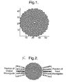
- an optical device comprises a waveguide structure having a photonic band structure region, the photonic band structure region including a first region having a first refractive index and an array of sub-regions having a second refractive index, the array of sub-regions being arranged in a Fibonacci spiral pattern.
- a Fibonacci spiral pattern can be found in nature in the arrangement of the seeds of a sunflower, florets of a cauliflower, pine cones and even in the shell of a Nautilus.
- a Fibonacci spiral pattern is an optimal packing system for the sub-regions surrounding a central region.
- the diffraction patterns formed by the array of sub-regions within the photonic band structure region are circular Bragg rings and this provides highly isotropic behaviour about a central region.
- the fact that the band structure is identical in all directions minimises the tolerance in placing input and output waveguides or fibres. This isotropy provides several benefits such as relaxed fabrication tolerances.
- mode divergence from the end of a waveguide or fibre is not critical using the optical device of the present invention.
- the band structure also possesses complete bandgaps for TE and TM polarisations even for relatively low dielectric contrasts. These two features make it extremely useful in laser design.
- the first region is made of a lasing material
- the structure exhibits an isotropic bandgap inhibiting emission in a particular wavelength range.
- the bandgap may include the stronger emission lines of the lasing material and so the structure can be used to suppress these spectral wavelengths and enhance other weaker spectral wavelengths.
- x n cos (n ⁇ ) ⁇ n
- n is the integer index for a point in the pattern.
- n is the integer index for a point in the pattern.
- n is the integer index for a point in the pattern.
- the optical device is a planar device including a substrate, a buffer layer, a core layer and a cladding layer, wherein the core layer is sandwiched between the buffer layer and the cladding layer.
- the array of sub-regions are holes formed in the first region.
- the holes are formed through the cladding and core layers.
- the holes are filled with a material having a third refractive index.
- the optical device may be a laser device including an active core layer.
- the active material may be a doped dielectric material such as erbium doped tantalum pentoxide, silicon nitride, silicon oxynitride or a lasing material such as gallium arsenide or indium phosphide.
- the array of holes are formed in a lasing cavity.
- the core is made from a lasing material and the photonic band structure region has a photonic bandgap covering at least one lasing wavelength of the core.
- the photonic band structure region may be optically pumped so as stimulate lasing.
- the device may further include an optical pump source coupled to the photonic band structure region for stimulating lasing.
- an electric current may be passed through the photonic band structure region or through the core region so as to stimulate lasing in which case the device may further include an electric current source coupled to the photonic band structure region for stimulating lasing.
- the optical device may be a vertical cavity surface emitting laser (VCSEL), in which the photonic band structure prohibits lasing in the plane of the spiral pattern and so emits a laser beam from a central cavity of the Fibonacci spiral pattern, perpendicular to the spiral pattern.
- VCSEL vertical cavity surface emitting laser
- the optical device could be a filtering device.
- the filtering device includes an input waveguide for directing optical signals to the photonic band structure region and an output waveguide for receiving optical signals from the photonic band structure region
- the device includes a first output waveguide and a second output waveguide, wherein the photonic band structure region is positioned between the input waveguide and the second output waveguide such that in use light passing to the first output waveguide from the input waveguide does not pass through the photonic bandgap region and light passing to the second output waveguide does pass through the photonic bandgap region, and is thereby filtered.
- the device can be arranged to couple light to the first output waveguide through the photonic bandgap region while light reflected from the photonic bandgap region is coupled to the second output waveguide.
- the waveguides may be ridge or rib type waveguides.
- the device may be used as an optical add-drop multiplexer (OADM).
- OADM optical add-drop multiplexer
- the photonic band structure region may include a defect in the vicinity of an output waveguide, the defect giving rise to a local defect passband within a bandgap, thereby in use allowing light at the defect wavelength to enter the output waveguide from the photonic band structure region.
- the optical device could be an optical coupler adapted to couple light diffracted by the photonic band structure region out of the plane of the waveguide structure to another optical device, preferably an optical fibre, positioned out of the plane of the waveguide structure.
- the optical device is an optical fibre comprising a central core surrounded by a Fibonacci spiral pattern of sub-regions which extend along at least a portion of the length of the optical fibre.
- This structure again gives rise to an isotropic photonic bandgap covering the wavelengths of operation of the optical fibre, thus confining optical signals carried by the optical fibre to the core region of the optical fibre.
- a method of processing an optical signal comprises the step of coupling an optical signal into an optical device comprising a waveguide structure having a photonic band structure region, the photonic band structure region including a first region having a first refractive index and an array of sub-regions having a second refractive index, the array of sub-regions being arranged in a Fibonacci spiral pattern.
- a method of manufacturing an optical device comprises the steps of forming a photonic band structure region in a waveguide structure, the photonic band structure region including a first region having a first refractive index and an array of sub-regions having a second refractive index, the array of sub-regions being arranged in a Fibonacci spiral pattern.
- the method may be a method of manufacturing an optical fibre comprising the steps of stacking tubes or rods of silica glass or polymers or plastics in a Fibonacci spiral pattern to form a preform, fusing the tubes or rods together and drawing the preform down in size in a fibre pulling tower.
- the tubes or rods are placed in a template or holder to hold them in the Fibonacci spiral pattern.
- the tubes or rods may be of different diameters allowing them to pack in a Fibonacci spiral pattern.
- the tubes or rods may be trapezoidal columns with a hole formed through, them longitudinally, which stack together to form a Fibonacci spiral pattern of holes.
- the method may also be a method of manufacturing an optical fibre comprising the steps of drilling a Fibonacci spiral pattern of holes in a block and drawing the block into a fibre.
- n is an integer.
- the size of the space or cavity at the centre of the pattern is determined by the lowest used value for n, the higher the lowest value for n, the larger the central cavity. This has important implications for the design of some types of laser devices as described below.
- This 2D Fibonacci spiral pattern provides an optimal packing system for rods in a dielectric medium surrounding a central cavity region and as such the geometry provides an ideal method for the generation of cavities in photonic quasicrystals.
- the inherent introduction of the central cavity during the pattern generation can be exploited in the design of photonic crystal lasers. Due to the optimal packing of the rods around a central cavity region the laser device can be made more compact than conventional photonic crystal lasers while still maintaining an isotropic bandgap with strong extinction ratios and fewer rods.
- the structure is highly isotropic around the central cavity region. This means that emission in all directions can be accurately predicted and controlled in all directions. It also has benefits in the coupling of light to and from the photonic band structure region. As shown in Figure 2 , the tolerance for placing input and output fibres accurately is reduced. In conventional photonic crystal devices the coupling of light into the correct mode is very important. This requires the coupling of light at an exact position and propagation direction. Additionally, the mode should be expanded out to form a plane wave to enhance the efficiency of coupling into the correct dispersion band. Owing to the isotropy of the bands in a quasicrystal based on a Fibonacci spiral pattern, the coupled mode shape and direction is not critical. The divergence of an input signal is therefore not a problem.
- the structure also possesses complete bandgaps forTE and TM polarisations. These bandgaps may or may not overlap depending on the particular design of the structure, ie the lattice pitch filling fraction, the waveguide geometrical and material properties, and the material properties of the rods. It is possible to provide a complete and absolute bandgap.
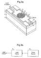
- Figure 3 shows a particular application of the Fibonacci spiral pattern in a planar waveguide structure.
- Figure 3a shows a laser design comprising a substrate 1 onto which a buffer layer 2 is formed.
- a core layer 3 comprising an active lasing material.
- the core layer 3 is covered by a cladding layer 4.
- Both the buffer layer 2 and the cladding layer 4 are oxides.
- the buffer layer 2 and the cladding layer 4 are of lower refractive index than the core layer 3.
- the structure incorporates a waveguide 5 formed between etched grooves 6 which extend through the cladding layer 4 and the core layer 3.
- the Fibonacci spiral pattern of holes 7 is formed around a central spot 8 to create a photonic band structure region.
- the holes extend through the cladding layer 4 and the core layer 3 and may extend wholly or partially into the buffer layer 2. Alternatively, the holes may exist only in the core layer 3. Light passing through the core layer 3 will impinge upon the photonic band structure region 7.
- the Fibonacci spiral pattern of holes 7 in the core layer 3 gives rise to a photonic bandgap which will prevent certain wavelengths from propagating through it.
- the bandgap may be tuned by selecting the size and spacing of the holes or by filling the holes with a material of appropriate refractive index, to suppress certain stronger lasing wavelengths which will enhance some weaker lasing wavelengths lying outside the bandgap.
- the holes may even be filled with a material having a tunable refractive index, such as liquid crystal.
- the highly isotropic nature of the pattern is beneficial as the bandgap resides in the same wavelength range for all directions of propagation, even for weak dielectric contrasts, providing good control of laser emission for all in-plane directions.
- Figure 3b is a schematic illustration of the laser 9 of Figure 3a , including a pump signal source 10 used to stimulate lasing.
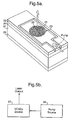
- Figure 4a shows another optical device, in this case a filter, incorporating the Fibonacci spiral pattern of holes that forms a photonic band structure region.
- Figure 4b is a cross-section of Figure 4a through the photonic band structure region.
- This structure includes a substrate layer 11 and a buffer layer 12 onto which a rib waveguide structure 13 is placed.
- the rib waveguide structure comprises a core layer 18 and a cladding layer 19 which are shown in Figure 4b .
- the cladding layer is not shown in Figure 4a .
- the rib waveguide structure 13 includes an input rib waveguide 14, a central region incorporating the Fibonacci spiral pattern 15 and output rib waveguides 16 and 17.
- the holes forming the Fibonacci spiral pattern extend through the cladding layer and the core layer and may extend wholly or partially into the buffer layer 12 as shown in Figure 4b . Alternatively, the holes may exist only in the core layer.
- a WDM optical signal propagating along the input rib waveguide 14 reaches the photonic band structure region 15 where the light couples into whispering gallery modes.
- Whispering gallery modes are modes which are radially confined within the band structure region by total internal reflection. As the Fibonacci spiral structure can only establish specific whispering gallery modes some of the input wavelengths are prevented from propagating through it.
- the relationship between the input signal and the Fibonacci spiral pattern is such that only a single wavelength from the input WDM optical signal may pass through it, which means that only a single wavelength of the signal is able to propagate to a first output waveguide 16. Those wavelengths prevented from propagating through the central region pass directly along the input rib waveguide 14 to a second output rib waveguide 17.
- the structure therefore acts as a drop filter.
- the same structure can also act as an optical add-drop multiplexer (OADM) by inputting and outputting optical signals from other waveguides.
- OADM optical add-drop multiplexer
- Figure 5 shows an example of a vertical cavity surface emitting laser (VCSEL) design in accordance with the present invention.
- the structure shown in Figure 5a includes a substrate layer 29, a buffer layer 21, a core layer 20 and a cladding layer 22.
- the core layer 20 is formed from an active material, such as a doped dielectric material such as erbium doped tantalum pentoxide, silicon nitride, silicon oxynitride or a lasing material such as gallium arsenide or indium phosphide, while the buffer 21 and cladding 22 layers are formed of a material (but not necessarily the same material) having a lower refractive index than the core layer 20, such as silicon dioxide.
- a doped dielectric material such as erbium doped tantalum pentoxide, silicon nitride, silicon oxynitride or a lasing material such as gallium arsenide or indium phosphide
- the buffer 21 and cladding 22 layers are formed
- a photonic band structure region is formed by etching a pattern of holes in a Fibonacci spiral pattern 23.
- the holes extend through the cladding layer 22 and the core layer 20 and may extend wholly or partially into the buffer layer 21. Alternatively, the holes may exist only in the core layer 20. These holes can be filled with another material or the same material as the cladding.
- Grooves 24 are etched around the photonic bandgap region to confine light such that the structure inhibits lasing in the plane of the waveguide or enhances out of plane diffraction.
- the photonic band structure region 23 is optically pumped via an optical input 25 to stimulate laser emission.
- the spacing and geometry of the holes in the Fibonacci spiral pattern are chosen according to the lasing wavelengths of the active material forming the core layer, such that the bandgap formed by the holes inhibits lasing in the plane of the waveguide.
- This provides for laser emission perpendicular to the plane of the waveguide as shown.
- the laser light is emitted from a central cavity 26 of the Fibonacci spiral pattern of holes 23.
- the beam of emitted light can be accurately controlled and can be designed to provide minimal divergence with a spot size approximately equal to the size of the central cavity 26.
- the spot size can therefore be controlled by an appropriate starting value for n, the index of the sub region closest to the centre. The larger the lowest value of n, the larger the central cavity will be.
- Figure 5b is a schematic illustration of the VCSEL 27 of Figure 5a , including a pump signal source 28 used to stimulate lasing in the VCSEL 27.
- FIG. 6 shows another example of a VCSEL design.
- the basic structure is the same as shown in Figure 5 .
- the core layer 30 is composed of a multilayer of active materials such as n-doped AlGaAs, GaAs and p-doped AlGaAs (starting with the first to be deposited).
- the cladding layer 32 is composed of p++ doped AIGaAs and the buffer layer 31 of an n++ doped AlGaAs. Instead of optically pumping the photonic bandgap region, lasing is induced by applying an electric current (generated by a source 37) through the active multilayer core 30.
- Top metal contacts 33 are placed on top of the cladding layer 32 all around the photonic bandgap region 34 and another contact 35 placed beneath or on the buffer layer 31.
- the geometry of the holes is again chosen to inhibit lasing of the core 30 in the plane of the waveguide.
- Laser emission then occurs from a central spot 36 perpendicular to the plane of the waveguide.
- the electrical signal applied across the core can be modulated. This modulates the photonic band gap arising from the Fibonacci spiral pattern. By modulating the band gap between covering the lasing wavelength and not covering the lasing wavelength a modulated laser output is obtained.
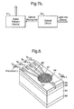
- Figure 7 shows an optical coupling structure.
- the structure shown in Figure 7a includes a substrate layer 46, a buffer layer 45, a core layer 41 and a cladding layer 44.
- the planar waveguide structure is as described above, with a Fibonacci spiral pattern of sub-regions 40 formed in the core layer 41 and in the cladding layer 44. Alternatively, the holes may exist only in the core layer.
- the spacing of the sub-regions 40 is such that it diffracts the impinging light from an input waveguide 42. Some of the light diffracts out of the plane of the waveguide.
- the diffraction pattern of the Fibonacci spiral pattern of sub-regions 40 forms sharp circular rings.
- the diffracted light forms cone-like beams which can be collected by an optical fibre 43 positioned above the waveguide as shown.
- conventional photonic crystals have diffraction patterns formed of an array of dots which cannot be easily collected).
- the collecting optical fibre 43 must be correctly aligned in order to collect the light efficiently.
- the angle through which the light is diffracted depends on a number of factors, primarily the geometry of the Fibonacci spiral pattern, but also the properties of the waveguide. If the light is strongly confined in the waveguide and the waveguide has a large effective refractive index the light will diverge strongly from the core and hence will diffract through a large angle.
- the angle of diffraction is also dependent on the wavelength of the light, which also determines the geometry of the Fibonacci spiral pattern.
- the diffraction pattern will also be different for different polarisation states as the light in the waveguide behaves differently for different polarisation states.
- the efficiency of coupling of light out of the plane of the waveguide can be further improved by forming the interfaces between the sub-regions and the core at an angle to the perpendicular.
- Figure 7b is a schematic representation of a device as shown in Figure 7a connected to an optical circuit.
- An optical signal processed in a photonic integrated circuit 50 can be coupled into an optical fibre for transmission using a device 51 as shown in Figure 7a without the need for butt-coupling.
- the size of the photonic band structure region can be matched to the diameter of the optical fibre to give optimal mode coupling.
- FIG. 8 shows an example of a demultiplexer device in accordance with the present invention.
- the waveguide structure is a planar structure including a substrate layer 60, a buffer layer 61, a core layer 62 and a cladding layer 63.
- a Fibonacci spiral pattern of sub-regions 64 is formed in the core layer 62 and the cladding layer 63, to create a photonic band structure region. Alternatively, the holes may exist only in the core layer.
- An input waveguide 65, carrying a WDM signal is formed on one side of the photonic band structure region 64. The wavelengths of the multiplexed signal each lie within the bandgap.
- a plurality of output waveguides 66 are formed on the opposite side.
- the defects 67 can be formed by variation in the hole size or slight shift in the position of the hole. Alternatively, a slight difference in the hole depth can also provide defect tuning. Defects can also be introduced by filling the holes with a material of different refractive index. This filler material can also be tunable, for example a liquid crystal, and hence the wavelength selection can be tuned still further.
- the defects 67 each introduce a defect passband at a different wavelength within the bandgap formed as a result the Fibonacci spiral pattern, the passband corresponding to the wavelengths of the multiplexed signal.
- the output waveguides 66 therefore each receive that wavelength allowed to pass by the proximate defect and hence the whole device functions as a demultiplexer.
- the device can be operated in reverse to form a multiplexer.
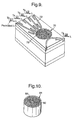
- Figure 9 shows a further demultiplexer design in accordance with the present invention.
- the device is very similar to the device shown in Figure 8 .
- Defects 73 are formed in the Fibonacci spiral pattern 70 in an identical fashion.
- the input 71 and output waveguides 72 are arranged tangential to the Fibonacci spiral pattern region 70 so that whispering gallery modes can couple into the Fibonacci spiral pattern from the input waveguide 71 and couple out into the output waveguides 72.
- the output wavelength for each waveguide is selected by the coupling from the Fibonacci spiral pattern whispering gallery mode to the defect and then the coupling from that to the specific output waveguide.
- FIG 10 shows an optical fibre in accordance with the present invention.
- the fibre comprises a central core 80 surrounded by a Fibonacci spiral pattern of sub-regions 81 of a different refractive index.
- the Fibonacci spiral pattern gives rise to an isotropic photonic bandgap covering the wavelengths of operation of the fibre, thus confining optical signals to the core region.
- the fibre can be formed by stacking tubes or rods of silica glass (or polymers or plastics) in a Fibonacci spiral pattern to form a preform. This structure is then fused together and drawn down in size in a fibre pulling tower. This generates a photonic quasicrystal fibre.
- the rods 90 could be placed in a template or holder 91 to hold them in the Fibonacci spiral pattern during fusing and drawing, as shown in Figure 11 . This prevents a loss of alignment from occurring during fusing and drawing.
- columns having a trapezoidal cross-section with a hole through each column as shown in Figure 12 could be used.
- the columns 95 have different geometries that allow them to stack perfectly in a Fibonacci spiral pattern.
- hollow rods of different diameters can be used, so that they stack perfectly in a Fibonacci spiral pattern. The smaller rods are placed in the centre with larger ones gradually added as they are packed in an outward fashion. The stack can then be placed in a tower and pulled.
- a glass block can be drilled to form holes in the correct positions and the whole block can then be pulled to form a fibre.
Landscapes
- Physics & Mathematics (AREA)
- Engineering & Computer Science (AREA)
- Optics & Photonics (AREA)
- Nanotechnology (AREA)
- General Physics & Mathematics (AREA)
- Chemical & Material Sciences (AREA)
- Biophysics (AREA)
- Life Sciences & Earth Sciences (AREA)
- Electromagnetism (AREA)
- Crystallography & Structural Chemistry (AREA)
- Condensed Matter Physics & Semiconductors (AREA)
- Microelectronics & Electronic Packaging (AREA)
- Optical Integrated Circuits (AREA)
Claims (32)
- Optische Vorrichtung (9, 27), umfassend: eine Wellenleiterstruktur (4, 5) mit einem Bereich mit photonischer Bandstruktur, wobei der Bereich mit photonischer Bandstruktur (7, 23) einen ersten Bereich mit einem ersten Brechungsindex und eine Gruppe von Unterbereichen (7, 23) mit einem zweiten Brechungsindex einschließt, dadurch gekennzeichnet, dass die Gruppe von Unterbereichen in einem Fibonacci-Spiralmuster (7, 23) angeordnet ist.
- Optische Vorrichtung (9, 27) nach Anspruch 1, wobei in einem kartesischen Koordinatensystem das Fibonacci-Spiralmuster definiert ist als xn = cos(nφ)√n yn = sin(nφ)√n mit φ π(√5-1), wobei n der ganzzahlige Index für einen Punkt in dem Muster ist.
- Optische Vorrichtung (9, 27) nach Anspruch 2, wobei das Muster unter Verwendung aufeinander folgender Werte von n erzeugt wird, wobei die Differenz zwischen aufeinander folgenden Werten 1 beträgt.
- Optische Vorrichtung (9, 27) nach Anspruch 2, wobei das Muster unter Verwendung aufeinander folgender Werte von n erzeugt wird, wobei die Differenz zwischen mindestens einem Paar aufeinander folgender Werte größer als 1 ist.
- Optische Vorrichtung (9, 27) nach einem vorangehenden Anspruch, wobei die optische Vorrichtung eine planare Vorrichtung ist, die ein Substrat (1, 29), eine Pufferschicht (2, 21), eine Kernschicht (3, 20) und eine Mantelschicht (4, 22) einschließt, wobei die Kernschicht (3, 20) zwischen der Pufferschicht (2, 21) und der Mantelschicht angeordnet ist.
- Optische Vorrichtung (9, 27) nach einem vorangehenden Anspruch, wobei die Unterbereiche im ersten Bereich ausgebildete Löcher sind.
- Optische Vorrichtung (9, 27) nach Anspruch 6, sofern abhängig von Anspruch 5, wobei die Löcher durch die Mantelschicht (4, 22) und die Kernschicht (3, 20) hindurch ausgebildet sind.
- Optische Vorrichtung (9, 27) nach Anspruch 6, wobei die Löcher (7, 23) mit einem Material gefüllt sind, das einen dritten Brechungsindex aufweist.
- Optische Vorrichtung (9, 27) nach einem vorangehenden Anspruch, wobei die optische Vorrichtung eine Laservorrichtung (9, 27) ist, die eine aktive Kernschicht (3, 20) einschließt.
- Optische Vorrichtung (9, 27) nach Anspruch 9, wobei die aktive Kernschicht (3, 20) aus einem dotierten dielektrischen Material, wie mit Erbium dotiertem Tantalpentoxid, Siliciumnitrid, Siliciumoxynitrid, oder einem Lasermaterial, wie Galliumarsenid oder Indiumphosphid, gefertigt ist.
- Optische Vorrichtung (9, 27) nach Anspruch 9 oder 10, wobei die Gruppe von Löchern in einem Laserhohlraum ausgebildet ist.
- Optische Vorrichtung (9, 27) nach einem der Ansprüche 9 bis 11, wobei der Kern (3, 20) aus einem Lasermaterial gefertigt ist und der Bereich mit photonischer Bandstruktur (7, 23) eine photonische Bandlücke aufweist, die mindestens eine Laserwellenlänge des Kerns abdeckt.
- Optische Vorrichtung (9, 27) nach Anspruch 12, ferner umfassend: eine mit dem Bereich mit photonischer Bandstruktur (7, 23) gekoppelte optische Pumpquelle (10, 28) zur Laseranregung.
- Optische Vorrichtung (9, 27) nach Anspruch 12, ferner umfassend: eine mit dem Bereich mit photonischer Bandstruktur (34) gekoppelte elektrische Stromquelle (37) zur Laseranregung.
- Optische Vorrichtung (9, 27) nach einem der Ansprüche 9 bis 14, wobei die Vorrichtung ein Vertical-Cavity Surface-Emitting Laser (VCSEL) (27) ist, bei dem die photonische Bandstruktur das Lasern in der Ebene des Spiralmusters verbietet und so bei Verwendung einen Laserstrahl von einem zentralen Hohlraum des Fibonacci-Spiralmusters, rechtwinklig zu dem Spiralmuster, aussendet.
- Optische Vorrichtung nach einem der Ansprüche 1 bis 8, wobei die Vorrichtung eine Filtervorrichtung (51) ist.
- Optische Vorrichtung (51) nach Anspruch 16, wobei die Filtervorrichtung einen Eingangswellenleiter (65) zum Richten optischer Signale zu dem Bereich mit photonischer Bandstruktur (64) und einen Ausgangswellenleiter (66) zum Empfangen optischer Signale von dem Bereich mit photonischer Bandstruktur (64) einschließt.
- Optische Vorrichtung (51) nach Anspruch 17, wobei die Vorrichtung einen ersten Ausgangswellenleiter (66) und einen zweiten Ausgangswellenleiter (66) einschließt, wobei der Bereich mit photonischer Bandstruktur (64) zwischen dem Eingangswellenleiter (65) und dem zweiten Ausgangswellenleiter (66) positioniert ist, derart dass bei Verwendung Licht, das vom Eingangswellenleiter (65) zum ersten Ausgangswellenleiter (66) passiert, nicht durch den Bereich mit photonischer Bandlücke (64) hindurch passiert und Licht, das zum zweiten Ausgangswellenleiter (66) passiert, durch den Bereich mit photonischer Bandlücke (64) hindurch passiert und dadurch gefiltert wird.
- Optische Vorrichtung (51) nach Anspruch 17 oder 18, wobei der Bereich mit photonischer Bandstruktur (64) eine Störstelle (67) in der Nähe eines Ausgangswellenleiters (66) einschließt, wobei die Störstelle (67) ein lokales Störstellendurchlassband innerhalb einer Bandlücke bewirkt, wodurch bei Verwendung Licht mit der Störstellenwellenlänge aus dem Bereich mit photonischer Bandstruktur (64) in den Ausgangswellenleiter (66) gelangen kann.
- Optische Vorrichtung (51) nach Anspruch 17, umfassend: einen ersten Ausgangswellenleiter (66) und einen zweiten Ausgangswellenleiter (66), wobei die Vorrichtung so angeordnet ist, dass sie Licht durch den Bereich mit photonischer Bandlücke (64) in den ersten Ausgangswellenleiter (66) einkoppelt, während vom Bereich mit photonischer Bandlücke (64) reflektiertes Licht in den zweiten Ausgangswellenleiter (66) eingekoppelt wird.
- Optische Vorrichtung (51) nach Anspruch 17, wobei die Wellenleiter (65, 66) ihrer Art nach Rippenwellenleiter sind.
- Optische Vorrichtung nach einem der Ansprüche 1 bis 8, wobei die optische Vorrichtung ein Optokoppler ist, der so angepasst ist, dass er durch den Bereich mit photonischer Bandstruktur (40) gebeugtes Licht aus der Ebene der Wellenleiterstruktur auskoppelt.
- Optische Vorrichtung nach einem der Ansprüche 1 bis 4, wobei die optische Vorrichtung ein Lichtwellenleiter (80, 81) ist, der einen zentralen Kern (80), umgeben von einem Fibonacci-Spiralmuster aus sich entlang mindestens eines Abschnitts der Länge des Lichtwellenleiters erstreckenden Unterbereichen (81), umfasst.
- Verfahren zur Verarbeitung eines optischen Signals, das folgenden Schritt umfasst: Einkoppeln eines optischen Signals in eine optische Vorrichtung (51), die eine Wellenleiterstruktur (62, 63) mit einem Bereich mit photonischer Bandstruktur (64) umfasst, wobei der Bereich mit photonischer Bandstruktur einen ersten Bereich mit einem ersten Brechungsindex und eine Gruppe von Unterbereichen mit einem zweiten Brechungsindex einschließt, dadurch gekennzeichnet, dass die Gruppe von Unterbereichen in einem Fibonacci-Spiralmuster (64) angeordnet ist.
- Verfahren zur Herstellung einer optischen Vorrichtung (9, 27, 51), das folgende Schritte umfasst: Ausbilden eines Bereichs mit photonischer Bandstruktur (7, 13, 64) in einer Wellenleiterstruktur, wobei der Bereich mit photonischer Bandstruktur einen ersten Bereich mit einem ersten Brechungsindex und eine Gruppe von Unterbereichen mit einem zweiten Brechungsindex einschließt, dadurch gekennzeichnet, dass die Gruppe von Unterbereichen in einem Fibonacci-Spiralmuster (7, 13, 64) angeordnet ist.
- Verfahren nach Anspruch 25, wobei in einem kartesischen Koordinatensystem das Fibonacci-Spiralmuster definiert ist als xn = cos(nφ)√n yn = sin(nφ)√n mit φ π(√5-1), wobei n der ganzzahlige Index für einen Punkt in dem Muster ist.
- Verfahren nach Anspruch 25 oder 26, wobei der erste Bereich aus Lasermaterial ausgebildet ist.
- Verfahren zur Herstellung eines Lichtwellenleiters (80, 81) nach einem der Ansprüche 25 bis 27, das folgende Schritte umfasst: Schichten von Röhren oder Stäben (90) aus Kieselglas oder Polymeren oder Kunststoffen in einem Fibonacci-Spiralmuster (81) zur Ausbildung eines Vorformlings, Verschmelzen der Röhren oder Stäbe miteinander und Kleinerziehen des Vorformlings in einem Faserziehturm.
- Verfahren zur Herstellung eines Lichtwellenleiters nach Anspruch 28, wobei die Röhren oder Stäbe (90) in einer Schablone oder Halterung (91) platziert sind, um sie in dem Fibonacci-Spiralmuster (81) zu halten.
- Verfahren zur Herstellung eines Lichtwellenleiters nach Anspruch 28 oder 29, wobei die Röhren oder Stäbe (90) unterschiedliche Durchmesser aufweisen.
- Verfahren zur Herstellung eines Lichtwellenleiters (80, 81) nach Anspruch 28, 29 oder 30, wobei die Röhren oder Stäbe (90) trapezförmige Säulen (95) mit einem in Längsrichtung durch sie hindurch ausgebildeten Loch (96) sind, die zusammengeschichtet sind, um ein Fibonacci-Spiralmuster von Löchern auszubilden.
- Verfahren zur Herstellung eines Lichtwellenleiters (80, 81) nach einem der Ansprüche 25 bis 27, das folgende Schritte umfasst: Bohren eines Fibonacci-Spiralmusters von Löchern in einen Block und Ziehen des Blocks zu einer Faser.
Applications Claiming Priority (3)
| Application Number | Priority Date | Filing Date | Title |
|---|---|---|---|
| US10/287,792 US6775448B2 (en) | 2002-11-05 | 2002-11-05 | Optical device |
| US287792 | 2002-11-05 | ||
| PCT/GB2003/004638 WO2004042440A1 (en) | 2002-11-05 | 2003-10-28 | Photonic crystal waveguide |
Publications (2)
| Publication Number | Publication Date |
|---|---|
| EP1558953A1 EP1558953A1 (de) | 2005-08-03 |
| EP1558953B1 true EP1558953B1 (de) | 2012-02-29 |
Family
ID=32175757
Family Applications (1)
| Application Number | Title | Priority Date | Filing Date |
|---|---|---|---|
| EP03810500A Expired - Lifetime EP1558953B1 (de) | 2002-11-05 | 2003-10-28 | Wellenleiter mit photonischem kristall |
Country Status (5)
| Country | Link |
|---|---|
| US (1) | US6775448B2 (de) |
| EP (1) | EP1558953B1 (de) |
| AT (1) | ATE547728T1 (de) |
| AU (1) | AU2003276404A1 (de) |
| WO (1) | WO2004042440A1 (de) |
Families Citing this family (36)
| Publication number | Priority date | Publication date | Assignee | Title |
|---|---|---|---|---|
| JP3743637B2 (ja) * | 2001-08-23 | 2006-02-08 | 独立行政法人理化学研究所 | フォトニック結晶および光導波素子 |
| JP2003206149A (ja) * | 2002-01-09 | 2003-07-22 | Nippon Telegr & Teleph Corp <Ntt> | 光ファイバの製造方法 |
| US6901189B1 (en) * | 2002-05-17 | 2005-05-31 | California Institute Of Technology | Graded-index whispering gallery mode resonators |
| US7833802B2 (en) * | 2002-11-21 | 2010-11-16 | Ada Technologies, Inc. | Stroboscopic liberation and methods of use |
| US20090093074A1 (en) * | 2004-04-23 | 2009-04-09 | Jae Hyung Yi | Light Emission From Silicon-Based Nanocrystals By Sequential Thermal Annealing Approaches |
| WO2005104317A1 (en) * | 2004-04-23 | 2005-11-03 | Massachusetts Institute Of Technology | Silicon rich nitride cmos-compatible light sources and si-based laser structures |
| US7509012B2 (en) * | 2004-09-22 | 2009-03-24 | Luxtaltek Corporation | Light emitting diode structures |
| US8377711B2 (en) * | 2005-04-04 | 2013-02-19 | Ada Technologies, Inc. | Stroboscopic liberation and methods of use |
| US7643718B2 (en) * | 2005-05-23 | 2010-01-05 | Research Foundation Of State University Of New York | Photonic waveguide device for modal control |
| EP1910875A4 (de) | 2005-07-08 | 2013-08-14 | Univ Princeton | Quasikristallinstrukturen und ihre verwendungen |
| US7388233B2 (en) * | 2005-10-17 | 2008-06-17 | Luminus Devices, Inc. | Patchwork patterned devices and related methods |
| WO2007047565A2 (en) * | 2005-10-17 | 2007-04-26 | Luminus Devices, Inc. | Patterned devices and related methods |
| US7391059B2 (en) * | 2005-10-17 | 2008-06-24 | Luminus Devices, Inc. | Isotropic collimation devices and related methods |
| US7348603B2 (en) * | 2005-10-17 | 2008-03-25 | Luminus Devices, Inc. | Anisotropic collimation devices and related methods |
| US20070085098A1 (en) * | 2005-10-17 | 2007-04-19 | Luminus Devices, Inc. | Patterned devices and related methods |
| WO2008073601A2 (en) * | 2006-10-31 | 2008-06-19 | Trustees Of Boston University | Deterministic aperiodic patterned dielectric and plasmonic materials for localized electromagnetic field enhancement |
| WO2008092118A2 (en) | 2007-01-25 | 2008-07-31 | Ada Technologies, Inc. | Stroboscopic signal amplification and surface enhanced raman spectroscopy |
| JP5063139B2 (ja) * | 2007-02-27 | 2012-10-31 | 日本航空電子工業株式会社 | フォトニック構造体 |
| US8179034B2 (en) * | 2007-07-13 | 2012-05-15 | 3M Innovative Properties Company | Light extraction film for organic light emitting diode display and lighting devices |
| US20090015142A1 (en) * | 2007-07-13 | 2009-01-15 | 3M Innovative Properties Company | Light extraction film for organic light emitting diode display devices |
| GB0801606D0 (en) * | 2008-01-29 | 2008-03-05 | Univ Kent Canterbury | Nanosensor based on resonance and surface plasmon effects |
| US20100110551A1 (en) * | 2008-10-31 | 2010-05-06 | 3M Innovative Properties Company | Light extraction film with high index backfill layer and passivation layer |
| US7957621B2 (en) * | 2008-12-17 | 2011-06-07 | 3M Innovative Properties Company | Light extraction film with nanoparticle coatings |
| CN102388513B (zh) * | 2009-02-11 | 2014-12-10 | 丹麦科技大学 | 混合垂直腔激光器 |
| US20100303414A1 (en) * | 2009-04-22 | 2010-12-02 | Atwater Jr Harry A | Chip-based slot waveguide spontaneous emission light sources |
| US20110013867A1 (en) * | 2009-05-28 | 2011-01-20 | De Los Santos Hector J | Reconfigurable Materials for Photonic System Embodiment |
| US8994540B2 (en) * | 2012-09-21 | 2015-03-31 | Google Inc. | Cover plate for a hazard detector having improved air flow and other characteristics |
| US9383512B2 (en) * | 2012-12-31 | 2016-07-05 | Infinera Corporation | Light absorption and scattering devices in a photonic integrated circuit that minimize optical feedback and noise |
| CN104466674B (zh) * | 2014-12-03 | 2017-07-14 | 中国科学院长春光学精密机械与物理研究所 | 基于光子晶体y波导的片上集成合束激光器及其制作方法 |
| US11038263B2 (en) | 2015-11-12 | 2021-06-15 | Duke University | Printed cavities for computational microwave imaging and methods of use |
| US10955614B1 (en) * | 2020-01-14 | 2021-03-23 | Globalfoundries U.S. Inc. | Optical fiber coupler structure having manufacturing variation-sensitive transmission blocking region |
| CN111599840B (zh) * | 2020-04-16 | 2023-03-31 | 北京迈格威科技有限公司 | 显示面板及电子设备 |
| CN112129730A (zh) * | 2020-09-30 | 2020-12-25 | 中国计量大学 | 基于向日葵型光子晶体结构的太赫兹波折射率传感器 |
| CN113422591B (zh) * | 2021-06-17 | 2023-06-09 | 哈尔滨工程大学 | 一种基于准周期结构的多通道滤波器 |
| CN114415194B (zh) * | 2022-04-01 | 2022-06-14 | 长沙思木锐信息技术有限公司 | 基于飞行时间探测的片上激光雷达系统 |
| CN114660717B (zh) * | 2022-04-01 | 2022-11-08 | 长沙思木锐信息技术有限公司 | 片上空间光调制器、散射聚焦系统及光调制方法 |
Family Cites Families (3)
| Publication number | Priority date | Publication date | Assignee | Title |
|---|---|---|---|---|
| GB9710062D0 (en) * | 1997-05-16 | 1997-07-09 | British Tech Group | Optical devices and methods of fabrication thereof |
| JP3522117B2 (ja) * | 1998-08-05 | 2004-04-26 | 日本電気株式会社 | 自己導波光回路 |
| GB0008546D0 (en) | 2000-04-06 | 2000-05-24 | Btg Int Ltd | Optoelectronic devices |
-
2002
- 2002-11-05 US US10/287,792 patent/US6775448B2/en not_active Expired - Lifetime
-
2003
- 2003-10-28 AT AT03810500T patent/ATE547728T1/de active
- 2003-10-28 EP EP03810500A patent/EP1558953B1/de not_active Expired - Lifetime
- 2003-10-28 WO PCT/GB2003/004638 patent/WO2004042440A1/en not_active Ceased
- 2003-10-28 AU AU2003276404A patent/AU2003276404A1/en not_active Abandoned
Also Published As
| Publication number | Publication date |
|---|---|
| ATE547728T1 (de) | 2012-03-15 |
| WO2004042440A1 (en) | 2004-05-21 |
| AU2003276404A1 (en) | 2004-06-07 |
| US6775448B2 (en) | 2004-08-10 |
| US20040086249A1 (en) | 2004-05-06 |
| EP1558953A1 (de) | 2005-08-03 |
Similar Documents
| Publication | Publication Date | Title |
|---|---|---|
| EP1558953B1 (de) | Wellenleiter mit photonischem kristall | |
| KR101448575B1 (ko) | 데이터를 반송 전자기파로 인코딩하는 광자 시스템 및 방법 | |
| EP1706767B1 (de) | Optische wellenkupplungsvorrichtung | |
| EP2513693B1 (de) | Photonische, integrierte schaltung mit einem wellenleiter-gitter-koppler | |
| EP1408353B1 (de) | Optische Verzögerungsvorrichtung und entsprechendes Verfahren | |
| CA2728879C (en) | Composite subwavelength-structured waveguide in optical systems | |
| US6873777B2 (en) | Two-dimensional photonic crystal device | |
| EP1627244B1 (de) | Ringresonator mit radialem bragg-reflektor | |
| JP5811273B2 (ja) | 光素子、光送信素子、光受信素子、ハイブリッドレーザ、光送信装置 | |
| Netti et al. | Visible photonic bandgap engineering in silicon nitride waveguides | |
| EP2887110A1 (de) | Integrierte photonische Koppler | |
| KR19980702842A (ko) | 광학 구조체와 그의 제조 방법 | |
| WO1998053535A1 (en) | Semiconductor micro-resonator device | |
| Olivier et al. | Improved 60 degree bend transmission of submicron-width waveguides defined in two-dimensional photonic crystals | |
| US20080050066A1 (en) | Resonator and device having the same | |
| JP2005274927A (ja) | フォトニック結晶デバイス | |
| JP2008298912A (ja) | 光学素子及び共振装置 | |
| KR20060123753A (ko) | 주파수 선택적 광 결합기-분리기 장치 | |
| US7224868B2 (en) | Radiation-free optical cavity | |
| JP2009294464A (ja) | リング共振器 | |
| JP2005345729A (ja) | 平面導波路素子および波長多重光通信装置 | |
| JP2025128968A (ja) | 光導波路素子 | |
| Lin et al. | Path diversity for non-geostationary orbit satellite communication systems using the constellation of GPS | |
| JP2006208524A (ja) | 光合分波素子およびそれを用いた光回路 |
Legal Events
| Date | Code | Title | Description |
|---|---|---|---|
| PUAI | Public reference made under article 153(3) epc to a published international application that has entered the european phase |
Free format text: ORIGINAL CODE: 0009012 |
|
| 17P | Request for examination filed |
Effective date: 20050526 |
|
| AK | Designated contracting states |
Kind code of ref document: A1 Designated state(s): AT BE BG CH CY CZ DE DK EE ES FI FR GB GR HU IE IT LI LU MC NL PT RO SE SI SK TR |
|
| AX | Request for extension of the european patent |
Extension state: AL LT LV MK |
|
| DAX | Request for extension of the european patent (deleted) | ||
| 17Q | First examination report despatched |
Effective date: 20071221 |
|
| RAP1 | Party data changed (applicant data changed or rights of an application transferred) |
Owner name: LUXTALTEK CORPORATION |
|
| RIC1 | Information provided on ipc code assigned before grant |
Ipc: G02B 6/12 20060101AFI20110801BHEP |
|
| GRAP | Despatch of communication of intention to grant a patent |
Free format text: ORIGINAL CODE: EPIDOSNIGR1 |
|
| GRAS | Grant fee paid |
Free format text: ORIGINAL CODE: EPIDOSNIGR3 |
|
| GRAA | (expected) grant |
Free format text: ORIGINAL CODE: 0009210 |
|
| AK | Designated contracting states |
Kind code of ref document: B1 Designated state(s): AT BE BG CH CY CZ DE DK EE ES FI FR GB GR HU IE IT LI LU MC NL PT RO SE SI SK TR |
|
| REG | Reference to a national code |
Ref country code: GB Ref legal event code: FG4D Ref country code: CH Ref legal event code: EP |
|
| REG | Reference to a national code |
Ref country code: DE Ref legal event code: R081 Ref document number: 60340169 Country of ref document: DE Owner name: NANOGAN LTD., GB Free format text: FORMER OWNER: MESOPHOTONICS LTD., CHILWORTH SCIENCE PARK, SOUTHAMPTON, GB |
|
| REG | Reference to a national code |
Ref country code: AT Ref legal event code: REF Ref document number: 547728 Country of ref document: AT Kind code of ref document: T Effective date: 20120315 |
|
| REG | Reference to a national code |
Ref country code: NL Ref legal event code: T3 |
|
| REG | Reference to a national code |
Ref country code: IE Ref legal event code: FG4D |
|
| REG | Reference to a national code |
Ref country code: SE Ref legal event code: TRGR |
|
| REG | Reference to a national code |
Ref country code: DE Ref legal event code: R096 Ref document number: 60340169 Country of ref document: DE Effective date: 20120426 |
|
| PG25 | Lapsed in a contracting state [announced via postgrant information from national office to epo] |
Ref country code: FI Free format text: LAPSE BECAUSE OF FAILURE TO SUBMIT A TRANSLATION OF THE DESCRIPTION OR TO PAY THE FEE WITHIN THE PRESCRIBED TIME-LIMIT Effective date: 20120229 Ref country code: GR Free format text: LAPSE BECAUSE OF FAILURE TO SUBMIT A TRANSLATION OF THE DESCRIPTION OR TO PAY THE FEE WITHIN THE PRESCRIBED TIME-LIMIT Effective date: 20120530 Ref country code: PT Free format text: LAPSE BECAUSE OF FAILURE TO SUBMIT A TRANSLATION OF THE DESCRIPTION OR TO PAY THE FEE WITHIN THE PRESCRIBED TIME-LIMIT Effective date: 20120629 Ref country code: BE Free format text: LAPSE BECAUSE OF FAILURE TO SUBMIT A TRANSLATION OF THE DESCRIPTION OR TO PAY THE FEE WITHIN THE PRESCRIBED TIME-LIMIT Effective date: 20120229 |
|
| REG | Reference to a national code |
Ref country code: AT Ref legal event code: MK05 Ref document number: 547728 Country of ref document: AT Kind code of ref document: T Effective date: 20120229 |
|
| PG25 | Lapsed in a contracting state [announced via postgrant information from national office to epo] |
Ref country code: CY Free format text: LAPSE BECAUSE OF FAILURE TO SUBMIT A TRANSLATION OF THE DESCRIPTION OR TO PAY THE FEE WITHIN THE PRESCRIBED TIME-LIMIT Effective date: 20120229 |
|
| PG25 | Lapsed in a contracting state [announced via postgrant information from national office to epo] |
Ref country code: DK Free format text: LAPSE BECAUSE OF FAILURE TO SUBMIT A TRANSLATION OF THE DESCRIPTION OR TO PAY THE FEE WITHIN THE PRESCRIBED TIME-LIMIT Effective date: 20120229 Ref country code: RO Free format text: LAPSE BECAUSE OF FAILURE TO SUBMIT A TRANSLATION OF THE DESCRIPTION OR TO PAY THE FEE WITHIN THE PRESCRIBED TIME-LIMIT Effective date: 20120229 Ref country code: CZ Free format text: LAPSE BECAUSE OF FAILURE TO SUBMIT A TRANSLATION OF THE DESCRIPTION OR TO PAY THE FEE WITHIN THE PRESCRIBED TIME-LIMIT Effective date: 20120229 Ref country code: EE Free format text: LAPSE BECAUSE OF FAILURE TO SUBMIT A TRANSLATION OF THE DESCRIPTION OR TO PAY THE FEE WITHIN THE PRESCRIBED TIME-LIMIT Effective date: 20120229 Ref country code: SI Free format text: LAPSE BECAUSE OF FAILURE TO SUBMIT A TRANSLATION OF THE DESCRIPTION OR TO PAY THE FEE WITHIN THE PRESCRIBED TIME-LIMIT Effective date: 20120229 |
|
| PG25 | Lapsed in a contracting state [announced via postgrant information from national office to epo] |
Ref country code: SK Free format text: LAPSE BECAUSE OF FAILURE TO SUBMIT A TRANSLATION OF THE DESCRIPTION OR TO PAY THE FEE WITHIN THE PRESCRIBED TIME-LIMIT Effective date: 20120229 |
|
| PLBE | No opposition filed within time limit |
Free format text: ORIGINAL CODE: 0009261 |
|
| STAA | Information on the status of an ep patent application or granted ep patent |
Free format text: STATUS: NO OPPOSITION FILED WITHIN TIME LIMIT |
|
| PG25 | Lapsed in a contracting state [announced via postgrant information from national office to epo] |
Ref country code: AT Free format text: LAPSE BECAUSE OF FAILURE TO SUBMIT A TRANSLATION OF THE DESCRIPTION OR TO PAY THE FEE WITHIN THE PRESCRIBED TIME-LIMIT Effective date: 20120229 |
|
| 26N | No opposition filed |
Effective date: 20121130 |
|
| REG | Reference to a national code |
Ref country code: DE Ref legal event code: R097 Ref document number: 60340169 Country of ref document: DE Effective date: 20121130 |
|
| PG25 | Lapsed in a contracting state [announced via postgrant information from national office to epo] |
Ref country code: ES Free format text: LAPSE BECAUSE OF FAILURE TO SUBMIT A TRANSLATION OF THE DESCRIPTION OR TO PAY THE FEE WITHIN THE PRESCRIBED TIME-LIMIT Effective date: 20120609 |
|
| PG25 | Lapsed in a contracting state [announced via postgrant information from national office to epo] |
Ref country code: MC Free format text: LAPSE BECAUSE OF NON-PAYMENT OF DUE FEES Effective date: 20121031 |
|
| REG | Reference to a national code |
Ref country code: CH Ref legal event code: PL |
|
| PG25 | Lapsed in a contracting state [announced via postgrant information from national office to epo] |
Ref country code: LI Free format text: LAPSE BECAUSE OF NON-PAYMENT OF DUE FEES Effective date: 20121031 Ref country code: BG Free format text: LAPSE BECAUSE OF FAILURE TO SUBMIT A TRANSLATION OF THE DESCRIPTION OR TO PAY THE FEE WITHIN THE PRESCRIBED TIME-LIMIT Effective date: 20120529 Ref country code: CH Free format text: LAPSE BECAUSE OF NON-PAYMENT OF DUE FEES Effective date: 20121031 |
|
| REG | Reference to a national code |
Ref country code: IE Ref legal event code: MM4A |
|
| PG25 | Lapsed in a contracting state [announced via postgrant information from national office to epo] |
Ref country code: IE Free format text: LAPSE BECAUSE OF NON-PAYMENT OF DUE FEES Effective date: 20121028 |
|
| PG25 | Lapsed in a contracting state [announced via postgrant information from national office to epo] |
Ref country code: TR Free format text: LAPSE BECAUSE OF FAILURE TO SUBMIT A TRANSLATION OF THE DESCRIPTION OR TO PAY THE FEE WITHIN THE PRESCRIBED TIME-LIMIT Effective date: 20120229 |
|
| PG25 | Lapsed in a contracting state [announced via postgrant information from national office to epo] |
Ref country code: LU Free format text: LAPSE BECAUSE OF NON-PAYMENT OF DUE FEES Effective date: 20121028 |
|
| PG25 | Lapsed in a contracting state [announced via postgrant information from national office to epo] |
Ref country code: HU Free format text: LAPSE BECAUSE OF FAILURE TO SUBMIT A TRANSLATION OF THE DESCRIPTION OR TO PAY THE FEE WITHIN THE PRESCRIBED TIME-LIMIT Effective date: 20031028 |
|
| REG | Reference to a national code |
Ref country code: FR Ref legal event code: PLFP Year of fee payment: 14 |
|
| REG | Reference to a national code |
Ref country code: FR Ref legal event code: PLFP Year of fee payment: 15 |
|
| REG | Reference to a national code |
Ref country code: DE Ref legal event code: R081 Ref document number: 60340169 Country of ref document: DE Owner name: NANOGAN LTD., GB Free format text: FORMER OWNER: LUXTALTEK CORP., CHUNAN MIAOLI COUNTY 350, TW |
|
| REG | Reference to a national code |
Ref country code: GB Ref legal event code: 732E Free format text: REGISTERED BETWEEN 20180301 AND 20180307 |
|
| REG | Reference to a national code |
Ref country code: FR Ref legal event code: PLFP Year of fee payment: 16 |
|
| REG | Reference to a national code |
Ref country code: NL Ref legal event code: PD Owner name: NANOGAN LTD.; GB Free format text: DETAILS ASSIGNMENT: CHANGE OF OWNER(S), ASSIGNMENT; FORMER OWNER NAME: LUXTALTEK CORPORATION Effective date: 20180419 |
|
| REG | Reference to a national code |
Ref country code: FR Ref legal event code: CA Effective date: 20180530 Ref country code: FR Ref legal event code: TP Owner name: NANOGAN LTD, GB Effective date: 20180530 |
|
| PGFP | Annual fee paid to national office [announced via postgrant information from national office to epo] |
Ref country code: IT Payment date: 20210910 Year of fee payment: 19 |
|
| PGFP | Annual fee paid to national office [announced via postgrant information from national office to epo] |
Ref country code: SE Payment date: 20210929 Year of fee payment: 19 |
|
| PGFP | Annual fee paid to national office [announced via postgrant information from national office to epo] |
Ref country code: GB Payment date: 20220930 Year of fee payment: 20 |
|
| PGFP | Annual fee paid to national office [announced via postgrant information from national office to epo] |
Ref country code: FR Payment date: 20220930 Year of fee payment: 20 |
|
| PGFP | Annual fee paid to national office [announced via postgrant information from national office to epo] |
Ref country code: NL Payment date: 20221025 Year of fee payment: 20 |
|
| PGFP | Annual fee paid to national office [announced via postgrant information from national office to epo] |
Ref country code: DE Payment date: 20221003 Year of fee payment: 20 |
|
| REG | Reference to a national code |
Ref country code: DE Ref legal event code: R081 Ref document number: 60340169 Country of ref document: DE Owner name: QUANTUM NIL LTD. TAIWAN BRANCH, TW Free format text: FORMER OWNER: NANOGAN LTD., CARDIFF, GB Ref country code: DE Ref legal event code: R081 Ref document number: 60340169 Country of ref document: DE Owner name: QUANTUM NIL LTD., ROAD TOWN, VG Free format text: FORMER OWNER: NANOGAN LTD., CARDIFF, GB |
|
| REG | Reference to a national code |
Ref country code: NL Ref legal event code: PD Owner name: QUANTUM NIL LIMITED TAIWAN BRANCH; TW Free format text: DETAILS ASSIGNMENT: CHANGE OF OWNER(S), ASSIGNMENT; FORMER OWNER NAME: NANOGAN LTD. Effective date: 20230307 |
|
| REG | Reference to a national code |
Ref country code: GB Ref legal event code: 732E Free format text: REGISTERED BETWEEN 20230323 AND 20230329 |
|
| REG | Reference to a national code |
Ref country code: SE Ref legal event code: EUG |
|
| PG25 | Lapsed in a contracting state [announced via postgrant information from national office to epo] |
Ref country code: SE Free format text: LAPSE BECAUSE OF NON-PAYMENT OF DUE FEES Effective date: 20221029 |
|
| REG | Reference to a national code |
Ref country code: DE Ref legal event code: R071 Ref document number: 60340169 Country of ref document: DE |
|
| PG25 | Lapsed in a contracting state [announced via postgrant information from national office to epo] |
Ref country code: IT Free format text: LAPSE BECAUSE OF NON-PAYMENT OF DUE FEES Effective date: 20221028 |
|
| REG | Reference to a national code |
Ref country code: NL Ref legal event code: MK Effective date: 20231027 |
|
| REG | Reference to a national code |
Ref country code: GB Ref legal event code: PE20 Expiry date: 20231027 |
|
| PG25 | Lapsed in a contracting state [announced via postgrant information from national office to epo] |
Ref country code: GB Free format text: LAPSE BECAUSE OF EXPIRATION OF PROTECTION Effective date: 20231027 |
|
| PG25 | Lapsed in a contracting state [announced via postgrant information from national office to epo] |
Ref country code: GB Free format text: LAPSE BECAUSE OF EXPIRATION OF PROTECTION Effective date: 20231027 |