EP1557934A2 - Convertisseur courant continu - courant continu avec une diode Zener à coefficient de température substantiel de zéro - Google Patents
Convertisseur courant continu - courant continu avec une diode Zener à coefficient de température substantiel de zéro Download PDFInfo
- Publication number
- EP1557934A2 EP1557934A2 EP04257379A EP04257379A EP1557934A2 EP 1557934 A2 EP1557934 A2 EP 1557934A2 EP 04257379 A EP04257379 A EP 04257379A EP 04257379 A EP04257379 A EP 04257379A EP 1557934 A2 EP1557934 A2 EP 1557934A2
- Authority
- EP
- European Patent Office
- Prior art keywords
- zener diode
- transistor
- converter
- transformer
- voltage
- Prior art date
- Legal status (The legal status is an assumption and is not a legal conclusion. Google has not performed a legal analysis and makes no representation as to the accuracy of the status listed.)
- Withdrawn
Links
Images


Classifications
-
- H—ELECTRICITY
- H02—GENERATION; CONVERSION OR DISTRIBUTION OF ELECTRIC POWER
- H02M—APPARATUS FOR CONVERSION BETWEEN AC AND AC, BETWEEN AC AND DC, OR BETWEEN DC AND DC, AND FOR USE WITH MAINS OR SIMILAR POWER SUPPLY SYSTEMS; CONVERSION OF DC OR AC INPUT POWER INTO SURGE OUTPUT POWER; CONTROL OR REGULATION THEREOF
- H02M3/00—Conversion of DC power input into DC power output
- H02M3/22—Conversion of DC power input into DC power output with intermediate conversion into AC
- H02M3/24—Conversion of DC power input into DC power output with intermediate conversion into AC by static converters
- H02M3/28—Conversion of DC power input into DC power output with intermediate conversion into AC by static converters using discharge tubes with control electrode or semiconductor devices with control electrode to produce the intermediate AC
- H02M3/325—Conversion of DC power input into DC power output with intermediate conversion into AC by static converters using discharge tubes with control electrode or semiconductor devices with control electrode to produce the intermediate AC using devices of a triode or a transistor type requiring continuous application of a control signal
- H02M3/335—Conversion of DC power input into DC power output with intermediate conversion into AC by static converters using discharge tubes with control electrode or semiconductor devices with control electrode to produce the intermediate AC using devices of a triode or a transistor type requiring continuous application of a control signal using semiconductor devices only
- H02M3/338—Conversion of DC power input into DC power output with intermediate conversion into AC by static converters using discharge tubes with control electrode or semiconductor devices with control electrode to produce the intermediate AC using devices of a triode or a transistor type requiring continuous application of a control signal using semiconductor devices only in a self-oscillating arrangement
- H02M3/3385—Conversion of DC power input into DC power output with intermediate conversion into AC by static converters using discharge tubes with control electrode or semiconductor devices with control electrode to produce the intermediate AC using devices of a triode or a transistor type requiring continuous application of a control signal using semiconductor devices only in a self-oscillating arrangement with automatic control of output voltage or current
-
- H—ELECTRICITY
- H02—GENERATION; CONVERSION OR DISTRIBUTION OF ELECTRIC POWER
- H02M—APPARATUS FOR CONVERSION BETWEEN AC AND AC, BETWEEN AC AND DC, OR BETWEEN DC AND DC, AND FOR USE WITH MAINS OR SIMILAR POWER SUPPLY SYSTEMS; CONVERSION OF DC OR AC INPUT POWER INTO SURGE OUTPUT POWER; CONTROL OR REGULATION THEREOF
- H02M1/00—Details of apparatus for conversion
- H02M1/10—Arrangements incorporating converting means for enabling loads to be operated at will from different kinds of power supplies, e.g. from AC or DC
-
- H—ELECTRICITY
- H02—GENERATION; CONVERSION OR DISTRIBUTION OF ELECTRIC POWER
- H02M—APPARATUS FOR CONVERSION BETWEEN AC AND AC, BETWEEN AC AND DC, OR BETWEEN DC AND DC, AND FOR USE WITH MAINS OR SIMILAR POWER SUPPLY SYSTEMS; CONVERSION OF DC OR AC INPUT POWER INTO SURGE OUTPUT POWER; CONTROL OR REGULATION THEREOF
- H02M1/00—Details of apparatus for conversion
- H02M1/32—Means for protecting converters other than automatic disconnection
Definitions
- This invention relates to a DC/DC converter and, in particular, to a step-down DC/DC converter.
- the DC/DC converter is a power converter for converting a DC voltage (an input DC voltage) having a voltage level into another DC voltage (an output DC voltage) having anther voltage level.
- the DC/DC converter is also called a switching regulator, a switching power source, or a ringing choke converter.
- the DC/DC converter where the output DC voltage has the voltage level higher than that of the input DC voltage is called a step-up DC/DC converter.
- the DC/DC converter where the output DC voltage has the voltage level lower than that of the input DC voltage is called a step-down DC/DC converter. This invention relates to the step-down DC/DC converter.
- the step-down DC/DC converter uses a transistor as a switch, switches the transistor, converts an input DC voltage into an AC voltage, steps the AC voltage down by using a transformer, and rectifiers it to convert an output DC voltage.
- the DC/DC converter of the type described comprises a transformer having a primary winding, a secondary winding, and an auxiliary winding.
- the auxiliary winding is called a feedback winding, a positive feedback winding, a feedback coil, or a base winding.
- a switching transistor is connected in series to the primary winding of the transformer. By making the switching transistor self-oscillation, energy is transmitted to the secondary winding.
- the DC/DC converter further comprises a control transistor for turning the switching transistor on or off.
- a feedback control circuit including a Zener diode is connected between the control transistor and the auxiliary winding.
- a switching power source for controlling current characteristics on a primary side is described in Japanese Published Patent Application (A) No. H11-98838 or JP 11-98838 A.
- the switching power source disclosed in JP 11-98838 A realizes stable performance which is independent of an input voltage and external factors such as environmental temperature.
- the switching power source uses, as the above-mentioned Zener diode, a diode having a positive temperature coefficient (e.g. a "positive temperature characteristic" where its Zener voltage becomes high when the temperature becomes high).
- the switching power source comprises a temperature detecting resistor for correcting variations of the current characteristics due to variations of the environmental temperature. That is, in JP 11-98838 A, the switching power source needs the temperature detecting resistor because of use of the diode having the positive temperature coefficient as the Zener diode.
- a ringing choke converter is disclosed in Japanese Published Patent Application (A) No. H8-275523 or JP 8-275523 A.
- the ringing choke converter disclosed in JP 8-275523 A comprises, as the Zener diode, a diode having a negative temperature coefficient (e.g. a "negative temperature characteristic" where its Zener voltage becomes low when the temperature becomes high).
- the ringing choke converter needs any temperature compensation because of use of the diode having the negative temperature coefficient as the Zener diode.
- a DC/DC converter is disclosed in Japanese Examined Utility Model Application Publication (Y) No. S56-5507 or JP 56-5507 Y
- the DC/DC converter disclosed in JP 56-5507 Y comprises a Zener diode for controlling an output voltage without the above-mentioned control transistor.
- the above-mentioned JP 56-5507 Y merely discloses the DC/DC converter which carries out an output voltage control on the primary side of the transformer but which does not carry out an output current control on the primary side of the transformer.
- a DC/DC converter comprises a transformer having a primary winding, a secondary winding, and an auxiliary winding, a switching transistor connected in series to the primary winding of the transformer, a control transistor for turning the switching transistor on or off, and a feedback control circuit connected between the control transistor and the auxiliary winding of the transformer.
- the feedback control circuit includes a Zener diode.
- the Zener diode has a substantially zero temperature coefficient.
- the Zener diode may have a Zener voltage which lies in a range between 5 volts and 6 volts.
- the temperature coefficient of said Zener diode may be selected so as to cancel a temperature characteristic of the control transistor.
- each of the switching transistor and the control transistor may be composed of, for example, an npn-type bipolar transistor.
- the switching transistor has a collector connected to an end of the primary winding while the switching transistor has an emitter which is grounded.
- the control transistor has a collector connected to a base of the switching transistor, while the control transistor has an emitter which is grounded.
- the auxiliary winding has an end which is grounded.
- the feedback control circuit is inserted between another end of the auxiliary winding and a base of the control transistor.
- the feedback control circuit may comprise, for example, the Zener diode which has an anode connected to a base of the control transistor and a cathode connected to the other end of the auxiliary winding, and a resistor connected in parallel to the Zener diode.
- the feedback control circuit may comprise the Zener diode having an anode connected to a base of the control transistor, a first resistor having an end connected to a cathode of the Zener diode, a second resistor which has an end connected to the base of the control transistor and another end connected to another end of the first transistor, and a third resistor connected between the other end of the second resistor and the other end of the auxiliary winding.
- the above-mentioned DC/DC converter further may comprise a capacitor having an end which is grounded, and a second Zener diode which has an anode connected to another end of the capacitor and a cathode connected to the base of the switching transistor.
- the conventional DC/DC converters use, as a Zener diode, a diode having a positive or a negative temperature coefficient. Therefore, it is understood that various temperature compensations are necessary to the conventional DC/DC converters.
- the present co-inventors reached an idea that uses, as the Zener diode, a diode having a substantially zero temperature coefficient.
- Zener diode There are two causes why current flows abruptly when a voltage is applied to the Zener diode in a reverse direction.
- One cause is a Zener breakdown due to a tunnel effect.
- Another cause is an avalanche breakdown due to an avalanche effect.
- the Zener diode is a diode where both effects are mixed little by little.
- the Zener breakdown dominates in the Zener diode having a relatively low Zener voltage while the avalanche breakdown dominates in the Zener diode having a relatively high Zener voltage.
- Both of the Zener breakdown and the avalanche breakdown are mixed at a proper rate in the Zener diode having the Zener voltage of about 5 volts.
- the description will proceed to a temperature characteristic of the Zener diode.
- the tunnel effect has a negative temperature coefficient.
- the avalanche effect has a positive temperature coefficient.
- the temperature characteristic of the Zener diode largely changes dependent on the Zener voltage.
- the tunnel effect and the avalanche effect are effective at the similar rate when the Zener voltage is equal to about 5 volts, the both temperature coefficients are cancelled to each other, whereby the Zener voltage hardly changes even if the temperature changes.
- control transistor has a temperature characteristic.
- a transistor has a negative temperature characteristic of -2mV/°C which is generally used. As a result, it is necessary to take account of the temperature characteristic of the control transistor.
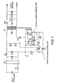
- the illustrated DC/DC converter comprises a transformer T1 having a primary winding N P , a secondary winding N S , and an auxiliary winding N B .
- the DC/DC converter includes, on a primary side of the transformer T1, a rectifying circuit D1, a first input capacitor C1, an input inductor L1, a second input capacitor C2, a switching transistor Q1, a control transistor Q2, a control feedback circuit (which will later be described), and so on.
- the first input capacitor C1, the input inductor L1, and the second input capacitor C2 constitute a smoothing circuit.
- An AC power source is connected to the rectifying circuit D1 through a resistor R1.
- the illustrated AC power source generates, as an input AC voltage, a voltage between 100 volts and 240 volts.
- the input AC voltage is rectified by the rectifying circuit D1, is smoothed by the above-mentioned smoothing circuit, and is stored in the second input capacitor C2 as an input DC voltage.
- the switching transistor Q1 is connected in series to the primary winding N P of the transformer T1.
- the second input capacitor C2 has an end connected to an end of the primary winding N P of the transformer T1.
- the illustrated switching transistor Q1 consists of an npn-type bipolar transistor.
- the primary winding N P of the transformer T1 has another end connected to a collector of the switching transistor Q1.
- the switching transistor Q1 has an emitter which is grounded.
- Resistors R2 and R3 are connected in series between a base of the switching transistor Q1 and the end of the second input capacitor C2.
- the input DC voltage is applied to the primary winding N P of the transformer T1 to turn the input DC voltage on or off by the switching transistor Q1.
- the control transistor Q2 is for turning the switching transistor Q1 on or off.
- the feedback control circuit which will be presently described, is connected.
- the control transistor Q2 consists of an npn-type bipolar transistor.
- the feedback control circuit comprises resistors R5, R6, R7 and a Zener diode D5.
- the resistors R5 and R6 are connected in series between a base of the control transistor Q2 and one end of the auxiliary winding N B of the transformer T1.
- the resistor R7 and the Zener diode D5 are connected in series between both ends of the resistor R5.
- the control transistor Q2 has an emitter which is grounded. Between the base and the emitter of the control transistor Q2, a capacitor C5 is connected. Between the end of the auxiliary winding N B of the transformer T1 and an collector of the control transistor Q2, a resistor R8 and a capacitor C6 are connected in series. The collector of the control transistor Q2 is connected to the base of the switching transistor Q1.
- a capacitor C3 has an end which is grounded.
- the capacitor C3 has another end which is connected to the base of the switching transistor Q1 through a Zener diode D2 and which is connected to the end of the auxiliary winding N B of the transformer T1 through a diode D3.
- the capacitor C6, and the resistor R8 are connected in series.
- the Zener diode D5 has a diode having a substantially zero temperature coefficient. More specifically, the Zener diode D5 has a Zener voltage which lies in a range between 5 volts and 6 volts. As a result, the illustrated DC/DC converter does not need a particular part for temperature compensation.
- the feedback control circuit serves as an output current control circuit while the Zener diode D2 serves as an output voltage control circuit.
- the DC/DC converter comprises, on a secondary side of the transformer T1, a diode D6, a resistor R10, an output capacitor C7, and a Zener diode D7.
- the secondary winding N S of the transformer T1 has an end connected to a grounding terminal GND of the DC/DC converter and another end connected to a power source terminal +B of the DC/DC converter through the diode D6.
- the resistor R10, the capacitor C7, and the Zener diode D7 are connected in parallel between the power source terminal +B and the grounding terminal GND.
- an AC voltage is rectified by the diode D6 and is smoothed by the output capacitor C7 to produce a secondary output voltage between the power source terminal +B and the grounding terminal GND.
- the DC/DC converter produces the secondary output voltage of 6 volts and can flow an output current of 650 milliamperes from the power source terminal +B.
- the DC/DC converter having the above-mentioned structure, it is possible to control the output constant voltage and the constant current on the primary side of the transformer T1 in the manner which will later be described and to stabilize the output concerning input fluctuations of the AC input voltage (100 volts to 240 volts).
- a minus voltage of the auxiliary winding N B of the transformer T1 is controlled by the Zener diode D2 to control the secondary output voltage at a constant.
- the control transistor Q2 has the temperature characteristic. Accordingly, the temperature coefficient of the Zener diode D5 is selected so as to cancel the temperature characteristic of the control transistor Q2. As a result, as a whole of the DC/DC converter, a stable current characteristic is realized.
- Fig. 2 shows a temperature characteristic of the output voltage in the DC/DC converter illustrated in Fig. 1.
- the abscissa represents temperature [°C] and the ordinate represents current [mA].
- Fig. 2 shows results measured at three temperatures of -20°C, 25°C, and 60°C. It may be understood that results change linearly at intermediate temperatures.
- a temperature characteristic illustrated in Fig. 2 is obtained as follows.
- the DC/DC converter (product) used to measure has a rated output voltage/output current of 5.3 volts/600 milliamperes. When the output current flows 600 milliamperers or more, the output voltage reduces gradually.
- Date shown in Fig. 2 represent current values measured on a time when the output voltage is equal to 3.6 volts. That is, by changing the environmental temperature of the produce and by measuring the current value when the output voltage becomes 3.6 volts, the temperature characteristic shown in Fig. 2 is obtained.
- the measured results are settled in a dispersion range within about 10% at a temperature range between -20°C and 60°C. From such a fact, it is understood that the temperature characteristic is adjusted in a range where can sufficiently use as actual products.
- the AC power source is connected to the rectifying circuit D1 through a fuse F2.
- the illustrated AC power source generates an input AC voltage of AC 100 volts.
- the output terminals of the rectifying circuit D1 are connected to a smoothing circuit which consists of the first input capacitor C1, a first inductor L1, the second input capacitor C2, and a second inductor L2.
- the smoothing circuit has an end connected to an end of the primary winding N P of the transformer T1.
- the primary winding N P of the transformer T1 has another end connected to the collector of the switching transistor Q1.
- the switching transistor Q1 has a base connected to the end of the primary winding N P of the transformer T1 through the resistors R3 and R2 which are connected in series to each other. Between the base and the emitter of the switching transistor Q1, a diode D10 is connected. The emitter of the switching transistor Q1 is grounded through a fuse F1.
- the emitter of the switching transistor Q1 is connected to an end of the auxiliary winding N B of the transformer T1.
- Another end of the auxiliary winding N B of the transformer T1 is connected to the base of the control transistor Q2 through a feedback control circuit (an output current control circuit).
- the feedback control circuit comprises a parallel circuit which consists of the resistor R5 and a series circuit consisting of the Zener diode D5 and the resistor R7.
- Both ends of the auxiliary winding N B of the transformer T1, a capacitor C9 and a diode D11 are connected in series. Between a connecting point of the capacitor C9 and the diode D11 and the base of the control transistor Q2, a Zener diode D9 and a resistor R15 are connected in series.
- the resistor R8 and the capacitor C6 are connected in series.
- the collector of the control transistor Q2 is connected to the base of the switching transistor Q1.
- the emitter of the control transistor Q2 is connected to the base of the switching transistor Q1 through the diode D10.
- the secondary winding N S of the transformer T1 has an end connected to the power source terminal +B through a parallel circuit consisting of the diode D6 and a capacitor C9 and an inductor L2.
- the secondary winding N S of the transformer T1 has another end which is connected to the grounding terminal GND.
- the capacitor C7 and the Zener diode D7 are connected in parallel.
- a capacitor C18 is connected between the power source terminal +B and the grounding terminal GND.
- the DC/DC converter produces the secondary output voltage between the power source terminal +B and the grounding terminal GND.
- the DC/DC converter produces the secondary output voltage of 5.6 volts and can flows an output current of 700 milliamperes from the power source terminal +B.
- the DC/DC converter according to the second embodiment of this invention comprises a photocoupler IC1 for feeding the output voltage on the secondary side back to the primary side.
- the photocoupler IC1 comprises a photodiode and a phototransistor. The description will be made as regards a circuit for feeding back the output voltage.
- a resistor R17 and a Zener diode D8 are connected in series.
- a connecting point between the resistor R17 and the Zener diode D8 is connected to a cathode of the photodiode of the photocoupler IC1.
- the photodiode of the photocoupler IC1 has an anode which is connected to the grounding terminal GND through a capacitor C8 and which is connected to the power source terminal +B through a resistor R12 and the inductor L2.
- the phototransistor of the photocoupler IC1 has a collector which is connected to the other end of the auxiliary winding N B of the transformer T1 through the diode D11 and which is connected to the base of the control transistor Q2 through a series circuit consisting of the diode D9 and the resistor R15.
- the phototransistor of the photocoupler IC1 has an emitter connected to the base of the control transistor Q2 through a resistor R12.
- the DC/DC converter according to the second embodiment of this invention carries out the output voltage control by feeding the output voltage on the secondary side of the transformer T1 back to the primary side of the transformer T1 by using the photocoupler IC1.
- the Zener diode D5 as one part in the feedback control circuit has a diode having a substantially zero temperature coefficient. More specifically, the Zener diode D5 has a Zener voltage which lies in a range between 5 volts and 6 volts. As a result, the illustrated DC/DC converter does not need a particular part for temperature compensation.
- control transistor Q2 has the temperature characteristic. Accordingly, the temperature coefficient of the Zener diode D5 is selected so as to cancel the temperature characteristic of the control transistor Q2. As a result, as a whole of the DC/DC converter, a stable current characteristic is realized.
- the feedback control circuit may be not restricted to those in the above-mentioned embodiments.
Landscapes
- Engineering & Computer Science (AREA)
- Power Engineering (AREA)
- Dc-Dc Converters (AREA)
Applications Claiming Priority (2)
| Application Number | Priority Date | Filing Date | Title |
|---|---|---|---|
| JP2004016575 | 2004-01-26 | ||
| JP2004016575A JP4371212B2 (ja) | 2004-01-26 | 2004-01-26 | Dc/dcコンバータ |
Publications (2)
| Publication Number | Publication Date |
|---|---|
| EP1557934A2 true EP1557934A2 (fr) | 2005-07-27 |
| EP1557934A3 EP1557934A3 (fr) | 2006-05-17 |
Family
ID=34631966
Family Applications (1)
| Application Number | Title | Priority Date | Filing Date |
|---|---|---|---|
| EP04257379A Withdrawn EP1557934A3 (fr) | 2004-01-26 | 2004-11-29 | Convertisseur courant continu - courant continu avec une diode Zener à coefficient de température substantiel de zéro |
Country Status (5)
| Country | Link |
|---|---|
| US (1) | US7123488B2 (fr) |
| EP (1) | EP1557934A3 (fr) |
| JP (1) | JP4371212B2 (fr) |
| CN (1) | CN1649246A (fr) |
| CA (1) | CA2488903A1 (fr) |
Families Citing this family (15)
| Publication number | Priority date | Publication date | Assignee | Title |
|---|---|---|---|---|
| US7310244B2 (en) * | 2006-01-25 | 2007-12-18 | System General Corp. | Primary side controlled switching regulator |
| JP5042536B2 (ja) * | 2006-06-16 | 2012-10-03 | ローム株式会社 | 電源装置及びこれを備えた電気機器 |
| CN101471608A (zh) * | 2007-12-29 | 2009-07-01 | 群康科技(深圳)有限公司 | 开关电源电路 |
| US8027176B2 (en) * | 2008-10-08 | 2011-09-27 | K A C Japan Co., Ltd. | Switching power supply circuit |
| US8933649B2 (en) * | 2009-12-28 | 2015-01-13 | Power Integrations, Inc. | Power converter having a switch coupled between windings |
| US8558484B2 (en) * | 2009-12-28 | 2013-10-15 | Power Integrations, Inc. | Power converter having a switch coupled between windings |
| CN102255483A (zh) * | 2010-05-18 | 2011-11-23 | 日隆电子股份有限公司 | 隔离式电源转换器的一次侧回授系统的温度补偿电路及方法 |
| CN102468757B (zh) * | 2010-11-17 | 2015-03-25 | 通嘉科技股份有限公司 | 控制器、电源供应器与控制方法 |
| KR101818773B1 (ko) * | 2011-10-24 | 2018-02-22 | 삼성전자주식회사 | 공진 방식 무선 충전 시스템용 수신 전력 변환 장치 |
| US8988902B2 (en) * | 2011-11-15 | 2015-03-24 | Dialog Semiconductor, Inc. | Power converter controller IC having pins with multiple functions |
| CN103516236B (zh) * | 2012-06-15 | 2016-05-25 | Tdk株式会社 | 转换器 |
| EP3183942A1 (fr) * | 2014-08-19 | 2017-06-28 | Philips Lighting Holding B.V. | Circuit convertisseur de puissance à découpage |
| US10348181B2 (en) | 2014-12-29 | 2019-07-09 | Hyosung Heavy Industries Corporation | Power control apparatus for sub-module of MMC converter |
| KR102543891B1 (ko) * | 2015-08-10 | 2023-06-14 | 엘지전자 주식회사 | 전력변환장치 및 이를 구비하는 공기조화기 |
| US10418986B2 (en) * | 2015-12-14 | 2019-09-17 | Monolithic Power Systems, Inc. | Monolithic integrated circuit switch device with output current balancing for parallel-connection |
Family Cites Families (11)
| Publication number | Priority date | Publication date | Assignee | Title |
|---|---|---|---|---|
| US3268739A (en) | 1963-06-20 | 1966-08-23 | Dickson Electronics Corp | Semiconductor voltage reference system having substantially zero temperature coefficient |
| JPS5378788A (en) * | 1976-12-23 | 1978-07-12 | Hitachi Ltd | Temperature-compensation-type constant voltage element |
| JPS565507Y2 (fr) | 1977-01-24 | 1981-02-05 | ||
| JPS60219964A (ja) | 1984-04-16 | 1985-11-02 | Fujitsu Ltd | コンバ−タ回路 |
| JPH01310413A (ja) | 1988-06-08 | 1989-12-14 | Murata Mfg Co Ltd | 磁気フィードバック制御型高圧電源装置 |
| JPH04368469A (ja) | 1991-06-12 | 1992-12-21 | Nec Corp | スイッチング電源 |
| JPH08275523A (ja) | 1995-03-27 | 1996-10-18 | Oohira Denshi Kk | リンギングチョークコンバータ |
| JPH1198838A (ja) | 1997-09-19 | 1999-04-09 | Matsushita Electric Ind Co Ltd | 電流制御型スイッチング電源 |
| JPH11122924A (ja) * | 1997-10-17 | 1999-04-30 | Murata Mfg Co Ltd | 自励発振型スイッチング電源装置 |
| JP2001290544A (ja) | 2000-04-07 | 2001-10-19 | Seiko Epson Corp | 定電圧を生成するためのツェナーダイオード回路 |
| JP3578113B2 (ja) * | 2001-05-29 | 2004-10-20 | 株式会社村田製作所 | スイッチング電源装置 |
-
2004
- 2004-01-26 JP JP2004016575A patent/JP4371212B2/ja not_active Expired - Fee Related
- 2004-11-24 US US10/998,234 patent/US7123488B2/en not_active Expired - Fee Related
- 2004-11-29 CA CA002488903A patent/CA2488903A1/fr not_active Abandoned
- 2004-11-29 CN CNA2004100964215A patent/CN1649246A/zh active Pending
- 2004-11-29 EP EP04257379A patent/EP1557934A3/fr not_active Withdrawn
Also Published As
| Publication number | Publication date |
|---|---|
| AU2004233528A1 (en) | 2005-08-11 |
| CN1649246A (zh) | 2005-08-03 |
| US7123488B2 (en) | 2006-10-17 |
| JP4371212B2 (ja) | 2009-11-25 |
| US20050162872A1 (en) | 2005-07-28 |
| JP2005210859A (ja) | 2005-08-04 |
| EP1557934A3 (fr) | 2006-05-17 |
| CA2488903A1 (fr) | 2005-07-26 |
Similar Documents
| Publication | Publication Date | Title |
|---|---|---|
| EP1557934A2 (fr) | Convertisseur courant continu - courant continu avec une diode Zener à coefficient de température substantiel de zéro | |
| CN101017381B (zh) | 具有恒定电流输出的初级侧稳压电源系统 | |
| US6608768B2 (en) | Use of a rectified image voltage for controlling the switch on the primary side of a switched-mode power supply | |
| US6721192B1 (en) | PWM controller regulating output voltage and output current in primary side | |
| US5633787A (en) | Switch-mode power supply with control of output supply voltage and overcurrent | |
| KR20060044625A (ko) | 전압검출회로, 전원장치 및 반도체 장치 | |
| EP2056437A1 (fr) | Circuit d'alimentation électrique et système d'alimentation électrique | |
| JP3386016B2 (ja) | スイッチング電源装置 | |
| GB2451088A (en) | Regulating the output of a forward power converter | |
| JP2008005567A (ja) | スイッチング電源装置 | |
| JP3733440B2 (ja) | スイッチング電源 | |
| US20020172057A1 (en) | Power supply arrangement comprising a DC/DC converter | |
| US20030053322A1 (en) | Power supply regulating | |
| EP0665632B1 (fr) | Dispositif d'alimentation de puissance à découpage | |
| US11996763B2 (en) | Integrated circuit and power supply circuit | |
| JP3267730B2 (ja) | 自動電圧切換式電源回路 | |
| EP4060887A1 (fr) | Alimentation électrique dali optimisée en termes de coût et de taille | |
| JP3171068B2 (ja) | スイッチング電源 | |
| JP3807611B2 (ja) | スイッチング電源装置 | |
| KR100341415B1 (ko) | 축전지 전압공급회로 | |
| KR100208805B1 (ko) | 포워드컨버터 | |
| KR100685078B1 (ko) | 스위칭 모드 파워 서플라이의 펄스폭 제한 회로 | |
| JP2001119951A (ja) | スイッチング電源装置 | |
| JPH06153505A (ja) | リンギングチョ−クコンバ−タ | |
| JPH049034B2 (fr) |
Legal Events
| Date | Code | Title | Description |
|---|---|---|---|
| PUAI | Public reference made under article 153(3) epc to a published international application that has entered the european phase |
Free format text: ORIGINAL CODE: 0009012 |
|
| AK | Designated contracting states |
Kind code of ref document: A2 Designated state(s): AT BE BG CH CY CZ DE DK EE ES FI FR GB GR HU IE IS IT LI LU MC NL PL PT RO SE SI SK TR |
|
| AX | Request for extension of the european patent |
Extension state: AL HR LT LV MK YU |
|
| PUAL | Search report despatched |
Free format text: ORIGINAL CODE: 0009013 |
|
| AK | Designated contracting states |
Kind code of ref document: A3 Designated state(s): AT BE BG CH CY CZ DE DK EE ES FI FR GB GR HU IE IS IT LI LU MC NL PL PT RO SE SI SK TR |
|
| AX | Request for extension of the european patent |
Extension state: AL HR LT LV MK YU |
|
| RIC1 | Information provided on ipc code assigned before grant |
Ipc: H02M 1/10 20060101ALI20060327BHEP Ipc: H02M 3/338 20060101AFI20050512BHEP |
|
| 17P | Request for examination filed |
Effective date: 20061103 |
|
| AKX | Designation fees paid |
Designated state(s): AT BE BG |
|
| REG | Reference to a national code |
Ref country code: DE Ref legal event code: 8566 |
|
| RBV | Designated contracting states (corrected) |
Designated state(s): DE FR GB |
|
| STAA | Information on the status of an ep patent application or granted ep patent |
Free format text: STATUS: THE APPLICATION IS DEEMED TO BE WITHDRAWN |
|
| 18D | Application deemed to be withdrawn |
Effective date: 20100601 |