EP1555713A1 - RF MEMS Schalter und zugehöriges Herstellungsverfahren - Google Patents
RF MEMS Schalter und zugehöriges Herstellungsverfahren Download PDFInfo
- Publication number
- EP1555713A1 EP1555713A1 EP05000879A EP05000879A EP1555713A1 EP 1555713 A1 EP1555713 A1 EP 1555713A1 EP 05000879 A EP05000879 A EP 05000879A EP 05000879 A EP05000879 A EP 05000879A EP 1555713 A1 EP1555713 A1 EP 1555713A1
- Authority
- EP
- European Patent Office
- Prior art keywords
- layer
- substrate
- cap substrate
- forming
- mems switch
- Prior art date
- Legal status (The legal status is an assumption and is not a legal conclusion. Google has not performed a legal analysis and makes no representation as to the accuracy of the status listed.)
- Withdrawn
Links
Images









Classifications
-
- B—PERFORMING OPERATIONS; TRANSPORTING
- B81—MICROSTRUCTURAL TECHNOLOGY
- B81B—MICROSTRUCTURAL DEVICES OR SYSTEMS, e.g. MICROMECHANICAL DEVICES
- B81B7/00—Microstructural systems ; Auxiliary parts of microstructural devices or systems
- B81B7/0032—Packages or encapsulation
- B81B7/007—Interconnections between the MEMS and external electrical signals
-
- A—HUMAN NECESSITIES
- A45—HAND OR TRAVELLING ARTICLES
- A45D—HAIRDRESSING OR SHAVING EQUIPMENT; EQUIPMENT FOR COSMETICS OR COSMETIC TREATMENTS, e.g. FOR MANICURING OR PEDICURING
- A45D44/00—Other cosmetic or toiletry articles, e.g. for hairdressers' rooms
-
- H—ELECTRICITY
- H01—ELECTRIC ELEMENTS
- H01G—CAPACITORS; CAPACITORS, RECTIFIERS, DETECTORS, SWITCHING DEVICES, LIGHT-SENSITIVE OR TEMPERATURE-SENSITIVE DEVICES OF THE ELECTROLYTIC TYPE
- H01G5/00—Capacitors in which the capacitance is varied by mechanical means, e.g. by turning a shaft; Processes of their manufacture
- H01G5/16—Capacitors in which the capacitance is varied by mechanical means, e.g. by turning a shaft; Processes of their manufacture using variation of distance between electrodes
-
- H—ELECTRICITY
- H01—ELECTRIC ELEMENTS
- H01G—CAPACITORS; CAPACITORS, RECTIFIERS, DETECTORS, SWITCHING DEVICES, LIGHT-SENSITIVE OR TEMPERATURE-SENSITIVE DEVICES OF THE ELECTROLYTIC TYPE
- H01G5/00—Capacitors in which the capacitance is varied by mechanical means, e.g. by turning a shaft; Processes of their manufacture
- H01G5/40—Structural combinations of variable capacitors with other electric elements not covered by this subclass, the structure mainly consisting of a capacitor, e.g. RC combinations
-
- H—ELECTRICITY
- H01—ELECTRIC ELEMENTS
- H01H—ELECTRIC SWITCHES; RELAYS; SELECTORS; EMERGENCY PROTECTIVE DEVICES
- H01H1/00—Contacts
- H01H1/0036—Switches making use of microelectromechanical systems [MEMS]
-
- H—ELECTRICITY
- H01—ELECTRIC ELEMENTS
- H01P—WAVEGUIDES; RESONATORS, LINES, OR OTHER DEVICES OF THE WAVEGUIDE TYPE
- H01P1/00—Auxiliary devices
- H01P1/10—Auxiliary devices for switching or interrupting
- H01P1/12—Auxiliary devices for switching or interrupting by mechanical chopper
- H01P1/127—Strip line switches
-
- A—HUMAN NECESSITIES
- A45—HAND OR TRAVELLING ARTICLES
- A45D—HAIRDRESSING OR SHAVING EQUIPMENT; EQUIPMENT FOR COSMETICS OR COSMETIC TREATMENTS, e.g. FOR MANICURING OR PEDICURING
- A45D33/00—Containers or accessories specially adapted for handling powdery toiletry or cosmetic substances
- A45D33/006—Vanity boxes or cases, compacts, i.e. containing a powder receptacle and a puff or applicator
- A45D33/008—Vanity boxes or cases, compacts, i.e. containing a powder receptacle and a puff or applicator comprising a mirror
-
- A—HUMAN NECESSITIES
- A45—HAND OR TRAVELLING ARTICLES
- A45D—HAIRDRESSING OR SHAVING EQUIPMENT; EQUIPMENT FOR COSMETICS OR COSMETIC TREATMENTS, e.g. FOR MANICURING OR PEDICURING
- A45D33/00—Containers or accessories specially adapted for handling powdery toiletry or cosmetic substances
- A45D33/26—Containers or accessories specially adapted for handling powdery toiletry or cosmetic substances combined with other objects
-
- B—PERFORMING OPERATIONS; TRANSPORTING
- B81—MICROSTRUCTURAL TECHNOLOGY
- B81B—MICROSTRUCTURAL DEVICES OR SYSTEMS, e.g. MICROMECHANICAL DEVICES
- B81B2201/00—Specific applications of microelectromechanical systems
- B81B2201/01—Switches
- B81B2201/012—Switches characterised by the shape
- B81B2201/014—Switches characterised by the shape having a cantilever fixed on one side connected to one or more dimples
-
- B—PERFORMING OPERATIONS; TRANSPORTING
- B81—MICROSTRUCTURAL TECHNOLOGY
- B81C—PROCESSES OR APPARATUS SPECIALLY ADAPTED FOR THE MANUFACTURE OR TREATMENT OF MICROSTRUCTURAL DEVICES OR SYSTEMS
- B81C2203/00—Forming microstructural systems
- B81C2203/01—Packaging MEMS
- B81C2203/0118—Bonding a wafer on the substrate, i.e. where the cap consists of another wafer
-
- H—ELECTRICITY
- H01—ELECTRIC ELEMENTS
- H01H—ELECTRIC SWITCHES; RELAYS; SELECTORS; EMERGENCY PROTECTIVE DEVICES
- H01H57/00—Electrostrictive relays; Piezoelectric relays
- H01H2057/006—Micromechanical piezoelectric relay
-
- Y—GENERAL TAGGING OF NEW TECHNOLOGICAL DEVELOPMENTS; GENERAL TAGGING OF CROSS-SECTIONAL TECHNOLOGIES SPANNING OVER SEVERAL SECTIONS OF THE IPC; TECHNICAL SUBJECTS COVERED BY FORMER USPC CROSS-REFERENCE ART COLLECTIONS [XRACs] AND DIGESTS
- Y10—TECHNICAL SUBJECTS COVERED BY FORMER USPC
- Y10T—TECHNICAL SUBJECTS COVERED BY FORMER US CLASSIFICATION
- Y10T29/00—Metal working
- Y10T29/42—Piezoelectric device making
-
- Y—GENERAL TAGGING OF NEW TECHNOLOGICAL DEVELOPMENTS; GENERAL TAGGING OF CROSS-SECTIONAL TECHNOLOGIES SPANNING OVER SEVERAL SECTIONS OF THE IPC; TECHNICAL SUBJECTS COVERED BY FORMER USPC CROSS-REFERENCE ART COLLECTIONS [XRACs] AND DIGESTS
- Y10—TECHNICAL SUBJECTS COVERED BY FORMER USPC
- Y10T—TECHNICAL SUBJECTS COVERED BY FORMER US CLASSIFICATION
- Y10T29/00—Metal working
- Y10T29/49—Method of mechanical manufacture
- Y10T29/49002—Electrical device making
- Y10T29/49105—Switch making
-
- Y—GENERAL TAGGING OF NEW TECHNOLOGICAL DEVELOPMENTS; GENERAL TAGGING OF CROSS-SECTIONAL TECHNOLOGIES SPANNING OVER SEVERAL SECTIONS OF THE IPC; TECHNICAL SUBJECTS COVERED BY FORMER USPC CROSS-REFERENCE ART COLLECTIONS [XRACs] AND DIGESTS
- Y10—TECHNICAL SUBJECTS COVERED BY FORMER USPC
- Y10T—TECHNICAL SUBJECTS COVERED BY FORMER US CLASSIFICATION
- Y10T29/00—Metal working
- Y10T29/49—Method of mechanical manufacture
- Y10T29/49002—Electrical device making
- Y10T29/49117—Conductor or circuit manufacturing
Definitions
- the present invention relates to an RF MEMS switch and a fabrication method thereof, and more particularly, to an RF MEMS switch capable of controlling an RF signal by using a piezoelectric capacitor and a fabrication method thereof.
- RF MEMS radio frequency micro-electromechanical system
- an FET switch or a semiconductor switch such as a PIN diode, etc. is being widely used as a switch of information communication system.
- the switches have many disadvantages such as a high power loss, a distortion, and a non-linear characteristic at the time of being actuated.
- the RF MEMS switch using an electrostatic force requires a high voltage and has a low reliability in operation.
- an object of the present invention is to provide an RF MEMS switch capable of being actuated with a low driving voltage and a low consumption power by using a piezoelectric capacitor and capable of obtaining a high yield and a high reliability, and a fabrication method thereof.
- an RF MEMS switch comprising: a cap substrate having via holes at both sides thereof, the via hole provided with a connection line; a transmission line having a first transmission line and a second transmission line spaced from each other with a certain gap at a lower surface of the cap substrate; a ground line formed at both sides of the transmission line; a connection pad formed at an upper surface of the cap substrate, and electrically connected to the transmission line and the ground line by the connection line; a bottom substrate having a certain gap from the cap substrate; a piezoelectric capacitor formed at one side of a suspension layer formed at an upper surface of the bottom substrate, and actuated with a piezoelectric characteristic by receiving an external power; and a contact electrode formed at another side of the suspension layer and moved up and down by a displacement of the piezoelectric capacitor, for selectively turning on/off RF signals of the first signal transmission line and the second signal transmission line.
- a fabrication method of an RF MEMS switch comprising: sequentially forming a first suspension layer of a silicon nitride and a second suspension layer of a silicon oxide on an upper surface of a bottom substrate, and forming a piezoelectric capacitor composed of a first electrode layer, a piezoelectric layer, and a second electrode at one side of an upper surface of the second suspension layer; forming a contact electrode at another side of the upper surface of the second suspension layer; etching the first suspension layer and the second suspension layer of the rest region except the piezoelectric capacitor and the contact electrode; etching a part of the bottom substrate to release a gap between the first suspension layer and the bottom substrate, thereby completing the bottom substrate; etching a center part of a lower surface of a cap substrate to form a groove; forming via holes at both sides of the cap substrate and filling a metal in the via hole,
- an RF MEMS switch comprising: a cap substrate having via holes at both sides thereof, the via hole provided with a connection line; a signal transmission line formed at a lower surface of the cap substrate; a ground line formed at both sides of the signal transmission line; a connection pad corresponding to the signal transmission line and formed at an upper surface of the cap substrate so as to be electrically connected to the signal transmission line and the ground line by the connection line; a bottom substrate having a certain gap from the cap substrate; a piezoelectric capacitor formed at one side of a suspension layer formed at an upper surface of the bottom substrate with a first metal layer thereof being exposed, and actuated with a piezoelectric characteristic by receiving an external power; and a capacitor contact electrode formed at another side of the suspension layer and connected to the exposed first metal layer, for selectively turning on/off an RF signal of the signal transmission line by being moved up and down by a displacement of the piezoelectric capacitor.
- a fabrication method of an RF MEMS switch comprising: sequentially forming a first suspension layer of a silicon nitride and a second suspension layer of a silicon oxide on an upper surface of a bottom substrate, and forming a piezoelectric capacitor composed of a first electrode layer, a piezoelectric layer, and a second electrode at one side of an upper surface of the second suspension layer; patterning the second electrode layer and the piezoelectric layer and then etching so that a part of the first electrode layer can be exposed; forming a capacitor contact electrode at another side of the upper surface of the second suspension layer so that the exposed part of the first electrode layer can be covered; etching the first suspension layer and the second suspension layer of the rest region except the piezoelectric capacitor and the contact electrode; etching a part of the bottom substrate to release a gap between the first suspension layer and the bottom substrate, thereby completing the bottom substrate; etching a center part of a lower surface of a cap substrate
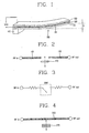
- FIG. 1 is a perspective view showing an operation of a piezoelectric capacitor using a piezoelectric power.
- a piezoelectric capacitor 160 is formed on a suspension layer 151.
- the piezoelectric capacitor 160 has a structure that a piezoelectric body 162 is formed between an upper electrode 163 and a lower electrode 161.
- the piezoelectric body 162 When a power is applied to the upper electrode 163 and the lower electrode 161, the piezoelectric body 162 is contracted or expanded thereby to be displaced as much as “h” upwardly.
- the "h” is determined by a thickness ratio of the suspension layer 151 and a piezoelectric constant of the piezoelectric body 162.
- PZT such as Pb(Zr(Zr, Ti)O 3
- power applied to the piezoelectric body 162 can be lowered, the piezoelectric body is smoothly actuated, and a fast switching speed can be obtained.
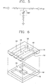
- FIG. 2 is a schematic diagram showing a structure of a resistive type RF MEMS switch
- FIG. 3 is an equivalent circuit showing the structure of the resistive type RF MEMS switch.
- a contact electrode 170 is moved up and down by the displacement of the piezoelectric body 160, thereby turning on/off a first signal line 121 and a second signal line 122 spaced from each other with a certain gap. According to this, an RF signal flowing to the first signal line 121 and the second signal line 122 is controlled.
- the first signal line 121 denotes an RF inline
- the second signal line 122 denotes an RF outline.
- FIG. 4 is a construction view showing a capacity type RF MEMS switch
- FIG. 5 is a circuit showing a structure of a resistive type RF MEMS switch.
- a capacitor contact electrode 270 connected to the piezoelectric capacitor 160 and composed of a first metal layer, a dielectric layer, and a second metal layer is spaced from a signal transmission line 220 with a certain gap.
- the piezoelectric body 162 When a power is applied to the piezoelectric capacitor 160, the piezoelectric body 162 is contracted or expanded thereby to be displaced as much as "h" upwardly. At this time, the capacitor contact electrode 270 is moved and served as a variable capacitor. According to this, a capacitor is increased towards a ground line (not shown), thereby turning off an RF signal flowing to the signal transmission line 220. When the piezoelectric capacitor 160 is operated, an RF signal is turned off and vice versa.
- an RF signal can be fast and easily controlled by using a piezoelectric capacitor actuated as electric energy thereof is converted into mechanical energy when an electric field is applied thereto.
- the RF MEMS switch of the present invention can be actuated with a voltage lower than 5V by using a piezoelectric power, and the RF MEMS switch can obtain a high reliability, a low voltage loss, and a fast switching speed.
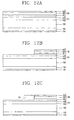
- FIG. 6 is a perspective view showing an RF MEMS switch according to a first embodiment of the present invention
- FIG. 7 is a longitudinal section view showing the RF MEMS switch according to the first embodiment of the present invention
- FIG. 8 is a longitudinal section view taken along line I-I of FIG. 7
- FIG. 9 is a plane view showing a bottom substrate of the RF MEMS switch according to the first embodiment of the present invention.
- an RF MEMS switch 100 comprises: a cap substrate 110 having via holes 111 at both sides thereof, the via hole 111 provided with a connection line 112; a signal transmission line 120 formed at a lower surface of the cap substrate 110, and having a first signal transmission line 121 and a second signal transmission line 122 spaced from each other with a certain gap; a ground line 130 formed at both sides of the signal transmission line 120; a connection pad 140 formed at an upper surface of the cap substrate 110, and electrically connected to the signal transmission line 120 and the ground line 130 by the connection line 112; a bottom substrate 150 having a certain gap from the cap substrate 110; a piezoelectric capacitor 160 formed at one side of a suspension layer 151 formed at an upper surface of the bottom substrate 150, and actuated with a piezoelectric characteristic when an external power is applied thereto; and a contact electrode 170 formed at another side of the suspension layer 151, for selectively turning on/off RF signals of the first signal transmission line 121
- the cap substrate 110 is formed as one signal transmission line 120 that connects an input terminal to an output terminal and two ground lines 130 are deposited on a silicon or a glass by a plating method.
- a bump 180 is formed between the cap substrate 110 and the bottom substrate 150 in order to maintain a certain gap between the cap substrate 110 and the bottom substrate 150.
- a solder bump or an organic bump can be used as the bump 180.
- the contact electrode 170 has a basic structure of Ti/Au or Cr/Au for a low resistance and an excellent bonding with the suspension layer.
- Mo, W, and Ir for a high mechanical intensity and melting point can be thinly deposited.
- the contact electrode 170 preferably has one structure of Ti/Au/Mo, Cr/Au/Mo, Ti/Au/W, Cr/Au/W, Ti/Au/Ir, and Cr/Au/Ir.
- the piezoelectric capacitor 160 is composed of a first metal layer 161, a piezoelectric layer 162, and a second metal layer 163.
- the piezoelectric layer 162 is Pb(Zr, Ti) and a ratio between the Zr and Ti is 6:4.
- FIG. 10 is a plane view showing another example of the bottom substrate of the RF MEMS switch according to the first embodiment of the present invention
- FIG. 11 is a plane view showing still another example of the bottom substrate of the RF MEMS switch according to the first embodiment of the present invention.
- a bottom substrate 150a four piezoelectric cantilevers 151a support a square contact electrode 170a.
- a bottom substrate 150b In a bottom substrate 150b, four piezoelectric cantilevers 151 b support a square contact electrode 170b.
- the suspension layer 151 that serves as a cantilever is deformed.
- the contact electrode 170 connects the first signal transmission line 121 and the second signal transmission line 122, thereby turning on the RF MEMS switch.
- the deformed suspension layer 151 is restored to the original state, thereby turning off the RF MEMS switch.
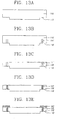
- FIGs. 12A to 12K are section views showing a fabrication process of an RF MEMS switch according to a first embodiment of the present invention.
- a fabrication method of an RF MEMS switch comprises: sequentially forming a first suspension layer of a silicon nitride and a second suspension layer of a silicon oxide on an upper surface of a bottom substrate, and forming a piezoelectric capacitor composed of a first electrode layer, a piezoelectric layer, and a second electrode at one side of an upper surface of the second suspension layer; forming a contact electrode at another side of the upper surface of the second suspension layer; etching the first suspension layer and the second suspension layer of the rest region except the piezoelectric capacitor and the contact electrode; etching a part of the bottom substrate to release a gap between the first suspension layer and the bottom substrate, thereby completing the bottom substrate; etching a center part of a lower surface of a cap substrate to form a groove; forming via holes at both sides of the cap substrate and filling a metal in the via hole, thereby forming a connection line; forming a signal transmission line and a ground line at an upper surface
- a first suspension layer 152 of a silicon nitride and a second suspension layer 153 of a silicon oxide are sequentially formed on an upper surface of a bottom substrate 150.
- suspension layers 154 and 155 of a silicon nitride are formed on a lower surface of the bottom substrate 150.
- a piezoelectric capacitor 160 composed of a first electrode layer 161, a piezoelectric layer 162, and a second electrode layer 163 is formed at one side of an upper surface of the second suspension layer 153.
- the first suspension layer 152 and the second suspension layer 153 are deposited on the upper surface of the bottom substrate 150 by using a low pressure chemical vapor deposition method.
- a part of the piezoelectric capacitor 160 is patterned and then etched, thereby removing unnecessary parts thereof.
- a contact electrode 170 is formed at another side of the upper surface of the second suspension layer 153.
- the first suspension layer 152 and the second suspension layer 153 of the rest region except the piezoelectric capacitor and the contact electrode are etched.
- a part 157 of the bottom substrate 150 is etched to release a gap between the first suspension layer 152 and the bottom substrate 150, thereby completing the bottom substrate 150.
- a wet etching is preferably performed by using one of KOH, hydrofluoric nitric acetic (HNA), tetra methyl ammonium hydroxide (TMAH), ethylene diamine pyrocatechol (EDP), and NaOH.
- HNA hydrofluoric nitric acetic
- TMAH tetra methyl ammonium hydroxide
- EDP ethylene diamine pyrocatechol
- a center part of a lower surface of a mother substrate to be served as a cap substrate 110 is etched, thereby forming a groove 113.
- the groove of the cap substrate is formed by using one of a plasma dry etching method, a sand blaster, or a laser cutting method.
- a via hole 111 is formed at both sides of the cap substrate 110, and a rear surface of the cap substrate 110 is polished until the via hole 111 is exposed by using a chemical mechanical polishing method. Then, metal such as gold, copper, or silver is filled in the via hole 111 by using an electro-analysis or a metal paste, thereby forming a connection line 112.
- a signal transmission line 120, a ground line 130 (referring to FIG. 12K), and a connection pad 140 are sequentially patterned to be deposited on the lower surface of the cap substrate 110.
- the signal transmission line 120 and the ground line 130 are electrically connected to the connection pad 140 by the connection line 112, thereby completing the cap substrate 110.
- the cap substrate 110 is bonded to the upper surface of the bottom substrate 150 by using a bump 180, thereby completing the RF MEMS switch 100.
- the gap between the contact electrode and the signal transmission line approximately corresponds to a sum between the height of the bump and the height of the etched part of the cap substrate.
- ground line of the piezoelectric capacitor and the ground line of the cap substrate are independently constructed in order to control the gap between the signal transmission line and the contact electrode.
- FIGs. 13A to 13F are section views showing a process for fabricating a .. cap substrate in the fabrication process of the MEMS switch according to the first embodiment of the present invention.
- both parts of a lower surface of a mother substrate to be served as a cap substrate 110' are etched, thereby forming a groove 113'.
- the groove 113' of the cap substrate 110' is formed by using one of a plasma dry etching method, a sand blaster, or a laser cutting method.
- a via hole 111' is formed at both sides of the cap substrate 110', and metal is filled in the via hole 111' thereby to form a connection line 112'.
- the lower surface of the cap substrate 110' is polished by using a chemical mechanical polishing method, thereby forming the via hole 111'.
- a signal transmission line 120', a ground line 130', and a connection pad 140' are sequentially patterned to be deposited on a lower surface of the cap substrate 110'. Then, the signal transmission line 120' and the ground line 130' are electrically connected to the connection pad 140' by the connection line 112', thereby completing the cap substrate 110'.
- both sides of the lower surface of the cap substrate 110' are etched to form the groove 113' and thereby the center part of the cap substrate 110' is downwardly protruded. According to this, when the RF MEMS switch is completed, the gap between the contact electrode and the signal transmission line is minimized.
- FIG. 14 is a perspective view showing an RF MEMS switch according to a second embodiment of the present invention
- FIG. 15 is a longitudinal section view showing the RF MEMS switch according to the second embodiment of the present invention
- FIG. 16 is a longitudinal section view taken along line II-II of FIG. 15
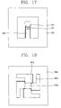
- FIG. 17 is a plane view showing a bottom substrate in the RF MEMS switch according to the second embodiment of the present invention.
- an RF MEMS switch 200 comprises: a cap substrate 210 having via holes 211 at both sides thereof, the via hole 211 provided with a connection line 212; a signal transmission line 220 formed at a lower surface of the cap substrate 210; a ground line 230 formed at both sides of the signal transmission line 220; a connection pad 240 corresponding to the signal transmission line 220 and formed at an upper surface of the cap substrate 210 so as to be electrically connected to the signal transmission line 220 and the ground line 230 by the connection line 212; a bottom substrate 250 having a certain gap from the cap substrate 210; a piezoelectric capacitor 260 formed at one side of a suspension layer 251 formed at an upper surface of the bottom substrate 250 with a part of a first metal layer 261 being exposed, and actuated with a piezoelectric characteristic when an external power is applied thereto; and a capacitor contact electrode 270 formed at another side of the suspension layer 251 and connected to the exposed first metal layer 261, for
- the piezoelectric capacitor 260 is formed as a first metal layer 261, a dielectric layer 262, and a second metal layer 263 are sequentially deposited. A part of the first metal layer 261 is exposed to outside.
- the capacitor contact electrode 270 preferably has a deposited structure composed of a first metal layer 271, a dielectric layer 272, and a second metal layer 273.
- the capacitor contact electrode 270 has a basic structure of Ti/Au or Cr/Au for a low resistance and an excellent bonding with the suspension layer.
- Mo, W, and Ir for a high mechanical intensity and melting point can be thinly deposited.
- the capacitor contact electrode 270 preferably has one structure of Ti/Au/Mo, Cr/Au/Mo, Ti/Au/W, Cr/Au/W, Ti/Au/Ir, and Cr/Au/Ir.
- the suspension layer 251 can be formed as a second suspension layer 253 of a silicon oxide is deposited on a first suspension layer 252 of a silicon nitride, as a second suspension layer 253 of a silicon oxide is deposited on a first suspension layer 252 of a silicon oxide, or as a second suspension layer 253 of a silicon nitride is deposited on a first suspension layer 252 of a silicon nitride.
- the second metal layer 272 of the capacitor contact electrode 270 is connected to the piezoelectric capacitor 260 by the first metal layer 261, thereby turning off the RF MEMS switch by flowing an RF signal to the ground line 230 when the capacitor contact electrode 270 is connected to the signal transmission line 220.
- FIG. 18 is a plane view showing another example of the bottom substrate in the RF MEMS switch according to the second embodiment of the present invention
- FIG. 19 is a plane view showing still another example of the bottom substrate in the RF MEMS switch according to the second embodiment of the present invention.
- a second metal layer (not shown) of a square capacitor contact electrode 270a is connected to a piezoelectric capacitor 260a by a first metal layer 261 a.
- a second metal layer (not shown) of a capacitor contact electrode 270b having a diamond shape is connected to a piezoelectric capacitor 260b by a first metal layer 261b.
- the suspension layer 251 that serves as a cantilever is deformed.
- the capacitor contact electrode 270 serves as a variable capacitor thereby to ground an RF signal flowing to the signal transmission line 220, thereby turning off the RF MEMS switch.
- the deformed suspension layer 251 is restored to the original state and thereby the RF MEMS switch is turned on.
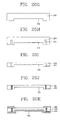
- FIGs. 20A to 20L are section views showing a fabrication process of the RF MEMS switch according to the second embodiment of the present invention.
- a fabrication method of an RF MEMS switch comprising: sequentially forming a first suspension layer of a silicon nitride and a second suspension layer of a silicon oxide on an upper surface of a bottom substrate, and forming a piezoelectric capacitor composed of a first electrode layer, a piezoelectric layer, and a second electrode at one side of an upper surface of the second suspension layer; patterning the second electrode layer and the piezoelectric layer and then etching so that a part of the first electrode layer can be exposed; forming a capacitor contact electrode at another side of the upper surface of the second suspension layer so that the exposed part of the first electrode layer can be covered; etching the first suspension layer and the second suspension layer of the rest region except the piezoelectric capacitor and the contact electrode; etching a part of the bottom substrate to release a gap between the first suspension layer and the bottom substrate, thereby completing the bottom substrate; etching a center part of a lower surface of a cap substrate
- FIGs. 20A to 20L a fabrication method of an RF MEMS switch according to a second embodiment of the present invention will be explained with reference to FIGs. 20A to 20L.
- a first suspension layer 252 of a silicon nitride and a second suspension layer 253 of a silicon oxide are sequentially formed on an upper surface of a bottom substrate 250.
- a piezoelectric capacitor 260 composed of a first electrode layer 261, a piezoelectric layer 262, and a second electrode layer 263 is formed at one side of an upper surface of the second suspension layer 253.
- the piezoelectric layer 262 and the second electrode layer 263 are patterned and then etched so that a part of the first electrode layer 261 can be exposed.
- a capacitor contact electrode 270 is formed at another side of the upper surface of the second suspension layer 253 so that the exposed part of the first electrode layer 261 can be covered.
- the first suspension layer 252 and the second suspension layer 253 of the rest region except the piezoelectric capacitor 260 and the capacitor contact electrode 270 are etched.
- a part 257 of the bottom substrate 250 is etched to release a gap between the first suspension layer 252 and the bottom substrate 250, thereby completing the bottom substrate 250.
- a center part of a lower surface of a mother substrate to be served as a cap substrate 210 is etched, thereby forming a groove 213.
- the groove of the cap substrate is formed by using one of a plasma dry etching method, a sand blaster, or a laser cutting method.
- a via hole 211 is formed at both sides of the cap substrate 210, and then a metal is filled in the via hole 211, thereby forming a connection line 212.
- the via hole 211 is formed by polishing the lower surface of the cap substrate 210 with a chemical mechanical polishing method.
- a signal transmission line 220, a ground line 230 (referring to FIG. 20L), and a connection pad 240 are formed on the lower surface of the cap substrate 210.
- the signal transmission line 220 and the ground line 230 are electrically connected to the connection pad 240 by the connection line 212, thereby completing the cap substrate 210.
- the cap substrate 210 is bonded to the upper surface of the bottom substrate 250 by using a bump 280, thereby completing the RF MEMS switch 200.
- a wet etching is preferably performed by using one of KOH, HNA, TMAH, EDP, NaOH, and XeF 2 gas phase.
- one of a plasma dry etching method, a sand blaster, or a laser cutting method is preferably used.
- the lower surface of the cap substrate is polished by using a chemical mechanical polishing method.
- the RF MEMS switch according to the present invention can be actuated with a low voltage and a low consumption power by using a piezoelectric capacitor, thereby having a high reliability and a high yield.
Landscapes
- Engineering & Computer Science (AREA)
- Power Engineering (AREA)
- Microelectronics & Electronic Packaging (AREA)
- Physics & Mathematics (AREA)
- Electromagnetism (AREA)
- Computer Hardware Design (AREA)
- Micromachines (AREA)
Applications Claiming Priority (2)
| Application Number | Priority Date | Filing Date | Title |
|---|---|---|---|
| KR2004003972 | 2004-01-19 | ||
| KR1020040003972A KR20050076149A (ko) | 2004-01-19 | 2004-01-19 | 압전 구동형 알에프 미세기전 시스템 스위치 및 그 제조방법 |
Publications (1)
| Publication Number | Publication Date |
|---|---|
| EP1555713A1 true EP1555713A1 (de) | 2005-07-20 |
Family
ID=34617472
Family Applications (1)
| Application Number | Title | Priority Date | Filing Date |
|---|---|---|---|
| EP05000879A Withdrawn EP1555713A1 (de) | 2004-01-19 | 2005-01-18 | RF MEMS Schalter und zugehöriges Herstellungsverfahren |
Country Status (3)
| Country | Link |
|---|---|
| US (3) | US7151425B2 (de) |
| EP (1) | EP1555713A1 (de) |
| KR (1) | KR20050076149A (de) |
Cited By (2)
| Publication number | Priority date | Publication date | Assignee | Title |
|---|---|---|---|---|
| US7545081B2 (en) | 2005-11-30 | 2009-06-09 | Samsung Electronics Co., Ltd. | Piezoelectric RF MEMS device and method of fabricating the same |
| WO2021097337A1 (en) * | 2019-11-13 | 2021-05-20 | Massachusetts Institute Of Technology | Micro-electromechanical (mem) power relay |
Families Citing this family (18)
| Publication number | Priority date | Publication date | Assignee | Title |
|---|---|---|---|---|
| US7763947B2 (en) * | 2002-04-23 | 2010-07-27 | Sharp Laboratories Of America, Inc. | Piezo-diode cantilever MEMS |
| JP4417861B2 (ja) * | 2005-01-31 | 2010-02-17 | 富士通株式会社 | マイクロスイッチング素子 |
| KR20070053515A (ko) * | 2005-11-21 | 2007-05-25 | 삼성전자주식회사 | Rf 멤스 스위치 및 그 제조방법 |
| KR20070074728A (ko) * | 2006-01-10 | 2007-07-18 | 삼성전자주식회사 | Mems 스위치 |
| JP4628275B2 (ja) * | 2006-01-31 | 2011-02-09 | 富士通株式会社 | マイクロスイッチング素子およびマイクロスイッチング素子製造方法 |
| WO2008042478A2 (en) * | 2006-06-09 | 2008-04-10 | Massachusetts Institute Of Technology | Wide band and radio frequency waveguide and hybrid integration in a silicon package |
| US8102638B2 (en) * | 2007-06-13 | 2012-01-24 | The University Court Of The University Of Edinburgh | Micro electromechanical capacitive switch |
| US7742275B2 (en) | 2007-08-31 | 2010-06-22 | Freescale Semiconductor, Inc. | MEMS capacitor with conductively tethered moveable capacitor plate |
| US7732991B2 (en) | 2007-09-28 | 2010-06-08 | Freescale Semiconductor, Inc. | Self-poling piezoelectric MEMs device |
| KR101039900B1 (ko) * | 2009-08-03 | 2011-06-09 | 주식회사 케이이씨 | 전자식 압력 스위치 및 그 제조 방법 |
| US20110242713A1 (en) * | 2010-04-06 | 2011-10-06 | Tyco Electronics Corporation | Planar voltage protection assembly |
| US20140202837A1 (en) * | 2010-06-14 | 2014-07-24 | Purdue Research Foundation | Low-cost process-independent rf mems switch |
| GB2494603B (en) | 2010-06-29 | 2016-05-04 | Ibm | Electromechanical switch device and method of operating the same |
| US8436638B2 (en) | 2010-12-10 | 2013-05-07 | International Business Machines Corporation | Switch to perform non-destructive and secure disablement of IC functionality utilizing MEMS and method thereof |
| SE537869C2 (sv) * | 2012-11-01 | 2015-11-03 | Silex Microsystems Ab | Substratgenomgående vior |
| US9496110B2 (en) * | 2013-06-18 | 2016-11-15 | Globalfoundries Inc. | Micro-electro-mechanical system (MEMS) structure and design structures |
| TWI508914B (zh) * | 2013-10-11 | 2015-11-21 | Pixart Imaging Inc | 具有增強結構強度之微機電元件 |
| KR101674635B1 (ko) * | 2014-03-27 | 2016-11-09 | 광운대학교 산학협력단 | 전기기계식 스위치와 반도체 트랜지스터가 융합된 능동형 다이오드 |
Citations (1)
| Publication number | Priority date | Publication date | Assignee | Title |
|---|---|---|---|---|
| US6426687B1 (en) * | 2001-05-22 | 2002-07-30 | The Aerospace Corporation | RF MEMS switch |
Family Cites Families (8)
| Publication number | Priority date | Publication date | Assignee | Title |
|---|---|---|---|---|
| DE1261045B (de) * | 1964-02-13 | 1968-02-08 | Nippon Electric Co | Keramisches piezoelektrisches Material |
| US6621387B1 (en) * | 2001-02-23 | 2003-09-16 | Analatom Incorporated | Micro-electro-mechanical systems switch |
| JP3818176B2 (ja) * | 2002-03-06 | 2006-09-06 | 株式会社村田製作所 | Rfmems素子 |
| KR100479687B1 (ko) * | 2002-05-30 | 2005-03-30 | 한국과학기술연구원 | 캔틸레버 센서 및 그 제조 방법 |
| KR100485787B1 (ko) * | 2002-08-20 | 2005-04-28 | 삼성전자주식회사 | 마이크로 스위치 |
| US7098577B2 (en) * | 2002-10-21 | 2006-08-29 | Hrl Laboratories, Llc | Piezoelectric switch for tunable electronic components |
| KR100492004B1 (ko) * | 2002-11-01 | 2005-05-30 | 한국전자통신연구원 | 미세전자기계적 시스템 기술을 이용한 고주파 소자 |
| US6909346B1 (en) * | 2003-04-18 | 2005-06-21 | Lockheed Martin Corporation | Switching arrangement using HDI interconnects and MEMS switches |
-
2004
- 2004-01-19 KR KR1020040003972A patent/KR20050076149A/ko not_active Ceased
-
2005
- 2005-01-18 EP EP05000879A patent/EP1555713A1/de not_active Withdrawn
- 2005-01-18 US US11/036,039 patent/US7151425B2/en not_active Expired - Fee Related
-
2006
- 2006-12-18 US US11/640,198 patent/US7765681B2/en not_active Expired - Fee Related
- 2006-12-28 US US11/646,293 patent/US7456713B2/en not_active Expired - Fee Related
Patent Citations (1)
| Publication number | Priority date | Publication date | Assignee | Title |
|---|---|---|---|---|
| US6426687B1 (en) * | 2001-05-22 | 2002-07-30 | The Aerospace Corporation | RF MEMS switch |
Cited By (3)
| Publication number | Priority date | Publication date | Assignee | Title |
|---|---|---|---|---|
| US7545081B2 (en) | 2005-11-30 | 2009-06-09 | Samsung Electronics Co., Ltd. | Piezoelectric RF MEMS device and method of fabricating the same |
| WO2021097337A1 (en) * | 2019-11-13 | 2021-05-20 | Massachusetts Institute Of Technology | Micro-electromechanical (mem) power relay |
| US11584643B2 (en) | 2019-11-13 | 2023-02-21 | Massachusetts Institute Of Technology | Micro-electromechanical (MEM) power relay |
Also Published As
| Publication number | Publication date |
|---|---|
| US20070109081A1 (en) | 2007-05-17 |
| US7765681B2 (en) | 2010-08-03 |
| US20070094864A1 (en) | 2007-05-03 |
| KR20050076149A (ko) | 2005-07-26 |
| US20050156694A1 (en) | 2005-07-21 |
| US7151425B2 (en) | 2006-12-19 |
| US7456713B2 (en) | 2008-11-25 |
Similar Documents
| Publication | Publication Date | Title |
|---|---|---|
| US7151425B2 (en) | RF MEMS switch and fabrication method thereof | |
| US6215644B1 (en) | High frequency tunable capacitors | |
| Park et al. | A fully wafer-level packaged RF MEMS switch with low actuation voltage using a piezoelectric actuator | |
| KR101092536B1 (ko) | 압전형 rf 멤스 소자 및 그 제조방법 | |
| JP4447940B2 (ja) | マイクロスイッチング素子製造方法およびマイクロスイッチング素子 | |
| US8530258B2 (en) | Method and apparatus for MEMS oscillator | |
| JP2008238330A (ja) | Mems装置およびこのmems装置を有する携帯通信端末 | |
| JP2009245877A (ja) | Memsスイッチおよびその製造方法 | |
| JP4465341B2 (ja) | 高周波マイクロマシンスイッチ及びその製造方法 | |
| CN104507853B (zh) | 形成半导体设备的方法 | |
| JP2007535797A (ja) | マイクロマシン技術(mems)スイッチ用のビーム | |
| TW200539204A (en) | Variable capacitor and manufacturing method thereof | |
| US6995440B2 (en) | MEMS switch having hexsil beam and method of integrating MEMS switch with a chip | |
| US20060091983A1 (en) | Electrostatic microswitch for low-voltage-actuation component | |
| US7619289B2 (en) | MEMS switch and method for manufacturing the same | |
| KR100650272B1 (ko) | 압전형 알에프 멤스 스위치 및 이를 이용한 다중 대역안테나 모듈 | |
| US8485417B1 (en) | Planar RF electromechanical switch | |
| KR20060022561A (ko) | 웨이퍼 단위 패키징 및 표면 미세 가공 기술을 이용한저가형 압전 rf mems 스위치 및 그 제조방법 | |
| US20050002596A1 (en) | Bonding method | |
| CN121506802A (zh) | 单刀双掷开关及其制备方法 | |
| WO2007099928A1 (ja) | 広帯域発振器 |
Legal Events
| Date | Code | Title | Description |
|---|---|---|---|
| PUAI | Public reference made under article 153(3) epc to a published international application that has entered the european phase |
Free format text: ORIGINAL CODE: 0009012 |
|
| 17P | Request for examination filed |
Effective date: 20050119 |
|
| AK | Designated contracting states |
Kind code of ref document: A1 Designated state(s): AT BE BG CH CY CZ DE DK EE ES FI FR GB GR HU IE IS IT LI LT LU MC NL PL PT RO SE SI SK TR |
|
| AX | Request for extension of the european patent |
Extension state: AL BA HR LV MK YU |
|
| RIN1 | Information on inventor provided before grant (corrected) |
Inventor name: LEE, HEE-CHULLOTTE-NAKCHEONDAE APT.108-1304 Inventor name: PARK, JAE-YEONG |
|
| AKX | Designation fees paid |
Designated state(s): AT BE BG CH CY CZ DE DK EE ES FI FR GB GR HU IE IS IT LI LT LU MC NL PL PT RO SE SI SK TR |
|
| 17Q | First examination report despatched |
Effective date: 20080424 |
|
| STAA | Information on the status of an ep patent application or granted ep patent |
Free format text: STATUS: THE APPLICATION IS DEEMED TO BE WITHDRAWN |
|
| 18D | Application deemed to be withdrawn |
Effective date: 20080905 |