EP1547166B1 - Light source module and method for production thereof - Google Patents
Light source module and method for production thereof Download PDFInfo
- Publication number
- EP1547166B1 EP1547166B1 EP03773459.7A EP03773459A EP1547166B1 EP 1547166 B1 EP1547166 B1 EP 1547166B1 EP 03773459 A EP03773459 A EP 03773459A EP 1547166 B1 EP1547166 B1 EP 1547166B1
- Authority
- EP
- European Patent Office
- Prior art keywords
- frame
- light source
- source module
- leds
- module according
- Prior art date
- Legal status (The legal status is an assumption and is not a legal conclusion. Google has not performed a legal analysis and makes no representation as to the accuracy of the status listed.)
- Expired - Lifetime
Links
Images

Classifications
-
- H—ELECTRICITY
- H10—SEMICONDUCTOR DEVICES; ELECTRIC SOLID-STATE DEVICES NOT OTHERWISE PROVIDED FOR
- H10W—GENERIC PACKAGES, INTERCONNECTIONS, CONNECTORS OR OTHER CONSTRUCTIONAL DETAILS OF DEVICES COVERED BY CLASS H10
- H10W90/00—Package configurations
-
- H—ELECTRICITY
- H10—SEMICONDUCTOR DEVICES; ELECTRIC SOLID-STATE DEVICES NOT OTHERWISE PROVIDED FOR
- H10H—INORGANIC LIGHT-EMITTING SEMICONDUCTOR DEVICES HAVING POTENTIAL BARRIERS
- H10H20/00—Individual inorganic light-emitting semiconductor devices having potential barriers, e.g. light-emitting diodes [LED]
- H10H20/80—Constructional details
- H10H20/85—Packages
- H10H20/8506—Containers
-
- H—ELECTRICITY
- H10—SEMICONDUCTOR DEVICES; ELECTRIC SOLID-STATE DEVICES NOT OTHERWISE PROVIDED FOR
- H10H—INORGANIC LIGHT-EMITTING SEMICONDUCTOR DEVICES HAVING POTENTIAL BARRIERS
- H10H20/00—Individual inorganic light-emitting semiconductor devices having potential barriers, e.g. light-emitting diodes [LED]
- H10H20/80—Constructional details
- H10H20/85—Packages
- H10H20/855—Optical field-shaping means, e.g. lenses
- H10H20/856—Reflecting means
-
- H—ELECTRICITY
- H10—SEMICONDUCTOR DEVICES; ELECTRIC SOLID-STATE DEVICES NOT OTHERWISE PROVIDED FOR
- H10W—GENERIC PACKAGES, INTERCONNECTIONS, CONNECTORS OR OTHER CONSTRUCTIONAL DETAILS OF DEVICES COVERED BY CLASS H10
- H10W72/00—Interconnections or connectors in packages
- H10W72/01—Manufacture or treatment
- H10W72/015—Manufacture or treatment of bond wires
- H10W72/01515—Forming coatings
-
- H—ELECTRICITY
- H10—SEMICONDUCTOR DEVICES; ELECTRIC SOLID-STATE DEVICES NOT OTHERWISE PROVIDED FOR
- H10W—GENERIC PACKAGES, INTERCONNECTIONS, CONNECTORS OR OTHER CONSTRUCTIONAL DETAILS OF DEVICES COVERED BY CLASS H10
- H10W72/00—Interconnections or connectors in packages
- H10W72/071—Connecting or disconnecting
- H10W72/075—Connecting or disconnecting of bond wires
-
- H—ELECTRICITY
- H10—SEMICONDUCTOR DEVICES; ELECTRIC SOLID-STATE DEVICES NOT OTHERWISE PROVIDED FOR
- H10W—GENERIC PACKAGES, INTERCONNECTIONS, CONNECTORS OR OTHER CONSTRUCTIONAL DETAILS OF DEVICES COVERED BY CLASS H10
- H10W72/00—Interconnections or connectors in packages
- H10W72/50—Bond wires
- H10W72/531—Shapes of wire connectors
- H10W72/5363—Shapes of wire connectors the connected ends being wedge-shaped
Definitions
- Such a light source module is eg in the published patent application DE 100 51 159 A1 described.
- the publication JP 2001-085748 A describes a light-emitting component.
- the frame is connected by the potting compound completely with the metal support on which the LEDs are arranged over an insulating layer, surface.
- the metal carrier expands differently from the frame, since the frame is usually not made of metal and thus the two materials have different coefficients of expansion.
- the invention is therefore based on the object of disclosing a light source module which also withstands strongly changing temperature conditions.
- This object is achieved in that the LEDs are surrounded by a frame between the frame and LEDs potting compound is arranged and the frame has expansion joints.
- the expansion joints can be realized either over extremely thin locations in the frame, which can deform in an expansion or via slots that go completely through the frame.
- the frame is segmented into a plurality of frame parts by expansion joints.
- a frame part preferably has a maximum of four recesses in which LEDs can be arranged. This number of recesses per frame part guarantees in a production of the frame made of plastic and the metal support made of aluminum, even at high temperature fluctuations high reliability and functionality.
- HUD Head-Up Display
- the segmentation of the frame for the production of the light source module is preferably carried out at the end of the process chain, i. after incorporation in the potting compound. This can e.g. done by means of a sawing device.
- FIG. 1 shows an LED light source module in partial sectional view.
- the light source module has two LEDs, one LED each having two optoelectronic components 1 arranged on a carrier substrate 2.
- the carrier substrate 2 is usually made of a good heat-conducting material and is arranged in each case via an intermediate insulating layer 3 and a carrier layer 5 on a metal support 4, which serves not only as a carrier, but also as a heat sink.
- the metal carrier 4 is preferably made of aluminum or copper to obtain a high heat dissipation.
- the insulating layer 3 integrated in the carrier substrate 2 generally consists of a silicon oxide layer 6 and a silicon nitride layer 7 applied to the silicon oxide layer 6.
- the silicon oxide layer is applied to a carrier layer 5 of silicon substrate.
- the insulating effect is achieved in particular by the silicon nitride and silicon oxide layers 7 and 6, wherein the silicon substrate 5 essentially serves only as a carrier material.
- On the insulating layer 7 are conductive metal pads 20 for contacting the LED.
- silicon layers can be applied extremely thinly and have a good thermal conductivity, these layers are ideal for electrical insulation and heat dissipation from the optoelectronic components 1 via the carrier substrates 2 to the metal carrier 4.
- a frame 10 is provided on the light source module mounted, which in each case encloses a carrier substrate 2 with mounted optoelectronic components 1.
- the frame 10 is glued to the underside with the circuit boards 8, so that the spaces in which the LEDs are located, can be poured out.
- the frame is first cast with reflective potting compound 11, such as white silicone or a filling compound with titanium oxide (TiO 2 ) or an epoxy resin mixed with titanium oxide particles.
- reflective potting compound 11 such as white silicone or a filling compound with titanium oxide (TiO 2 ) or an epoxy resin mixed with titanium oxide particles.
- the casting takes place until just below the upper edge of the carrier substrate 2, wherein the surface of the reflective potting compound 11 is concave to the inner edge of the frame 10.
- a potting of the interior is carried out with clear potting compound 12, for which purpose usually transparent silicone or transparent epoxy resin is used.
- the frame 10 is made for reasons of cost usually made of plastic, so that with strong temperature differences large loads respect.
- the LEDs result because the plastic frame 10 expands differently, as the usually made of aluminum metal support. 4
- expansion joints 13 are provided in the frame, over which the highly temperature-dependent expansion of the metal support 4 can be intercepted from aluminum.
- the expansion joints 13 may be formed as a strong tapered body in the frame 10, so that at this highly tapered body of the plastic Frame 10 can deform elastically under loads occurring.
- the expansion joints 13, as in FIG. 1 also be designed as a complete separation of the frame 10 at this point.
- a separating cut 14 proceed in the expansion joint 13, so that separate frame parts 10a and 10b arise.
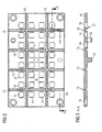
- FIG. 2 shows in a view from above the complete frame 10, as used for example for a light source module for a head-up display system (HUD system) in a motor vehicle.
- HUD system head-up display system
- the frame 10 has slaughterunddreisig recesses 14, in each of which a carrier substrate 2 with at least two optoelectronic devices 1, as in FIG. 1 represented, are arranged.
- the light points are arranged in a grid of 4.5 mm in 8 columns and 4 rows.
- Polychromic light points are obtained by arranging a plurality of optoelectronic components 1 of different color on a carrier substrate 2.
- the expansion joints 13 are arranged in a grid shape in the frame 10, so that the frame is divided into several segments by the grid-shaped expansion joints 13 ,
- a frame segment in this case comprises a maximum of four recesses 14th
- FIG. 3 shows the section AA FIG. 1 by the frame 10.
- the frame 10 is formed substantially flat and has on its underside pin 15, with which it can be mounted on the metal support 4. Furthermore are also provided mounting holes 16, which can also be used for shipment to the metal support.
- the recesses 14 are shown in cross section, which have on the underside small undercuts 17, so that the reflective potting compound 11 is also received positively.
- the frame on both sides of a trapezoidal recess which can either be chosen so that even the thin web absorbs the deformation or, as in FIG. 1 represented, at this point by means of a sawing device, the remaining web is severed with a separating cut 14.
- the separation can be done after completion of mounting the frame on the metal support 4 and the casting of the recesses 14.
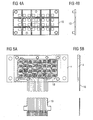
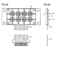
- FIGS. 4 to 6 schematically the assembly of the frame 10 is shown briefly.
- the FIGS. 4a to 6a each show the view from above, Figure 4b to 6b the side view.
- FIGS. 4a and 4b show the in the FIGS. 2 and 3 described framework
- FIGS. 5a and 5b show the metal support 4 with applied insulating and carrier layer and a flexible printed circuit board 18 arranged thereon with a flexible conductor connection 19, the carrier substrates 2 and the optoelectronic components 1 being applied to the flexible printed circuit board 18.
- FIGS. 6a and 6b show how the frame 10 is merely attached to the metal support 4 with the already applied flexible circuit board 18 and glued to it.
- the severing of the expansion joints 13 with the sawing device can already be done after this process step or only after the casting of the recesses 14.
Landscapes
- Led Device Packages (AREA)
Description
Die Erfindung betrifft ein Lichtquellemodul mit mehreren LEDs (LED = light emitting device), die isolierend mit einem Metallträger verbunden sind.The invention relates to a light source module with a plurality of LEDs (LED = light emitting device), which are connected in isolation with a metal support.
Ein derartiges Lichtquellenmodul ist z.B. in der Offenlegungsschrift
Die Druckschrift
Aus der noch nicht veröffentlichten deutschen Anmeldung mit der Anmeldungsnummer
Diese Art der Herstellung eines Lichtquellenmoduls funktioniert problemlos, wenn nur eine LED innerhalb des Rahmens angeordnet ist.This way of making a light source module works well when only one LED is placed inside the frame.
Sind jedoch mehrere LEDs in einem Rahmen angeordnet, ist der Rahmen durch die Vergußmasse komplett mit dem Metallträger, auf welchem die LEDs über eine Isolierschicht angeordnet sind, flächig verbunden.However, if several LEDs are arranged in a frame, the frame is connected by the potting compound completely with the metal support on which the LEDs are arranged over an insulating layer, surface.
Bei stark unterschiedlichen Temperaturbelastungen dehnt sich der Metallträger unterschiedlich zum Rahmen aus, da der Rahmen in der Regel nicht aus Metall besteht und somit die beiden Werkstoffe unterschiedliche Ausdehnungskoeffizienten aufweisen.At very different temperature loads, the metal carrier expands differently from the frame, since the frame is usually not made of metal and thus the two materials have different coefficients of expansion.
Durch die unterschiedlichen Ausdehnungskoeffizienten dieser beiden Bauteile kommt es zu Belastungen auf die LEDs, was somit Ausfälle einzelner LEDs bzw. so zur Zerstörung des gesamten Lichtquellenmoduls führen kann.Due to the different expansion coefficients of these two components, there are loads on the LEDs, which thus can cause failures of individual LEDs or so to the destruction of the entire light source module.
Der Erfindung liegt daher die Aufgabe zugrunde, ein Lichtquellenmodul aufzuzeigen, welches auch stark wechselnden Temperaturbedingungen Stand hält.The invention is therefore based on the object of disclosing a light source module which also withstands strongly changing temperature conditions.
Diese Aufgabe wird erfindungsgemäß dadurch gelöst, daß die LEDs von einem Rahmen umgeben sind, zwischen Rahmen und LEDs Vergußmasse angeordnet ist und der Rahmen Dehnfugen aufweist.This object is achieved in that the LEDs are surrounded by a frame between the frame and LEDs potting compound is arranged and the frame has expansion joints.
Durch das Einbringen der Dehnfugen in den Rahmen ist es möglich, die aus der nachveröffentlichten Patentanmeldung
Die Dehnfugen können entweder über extrem dünn gehaltene Stellen im Rahmen realisiert sein, die sich bei einer Ausdehnung verformen können bzw. auch über Schlitze, die komplett durch den Rahmen hindurchgehen.The expansion joints can be realized either over extremely thin locations in the frame, which can deform in an expansion or via slots that go completely through the frame.
Gemäß einer bevorzugten Ausführungsform ist der Rahmen in mehrere Rahmenteile durch Dehnfugen segmentiert.According to a preferred embodiment, the frame is segmented into a plurality of frame parts by expansion joints.
Hierbei weist ein Rahmenteil vorzugsweise maximal vier Aussparungen auf, in denen LEDs angeordnet werden können. Diese Anzahl von Aussparungen pro Rahmenteil garantiert bei einer Herstellung des Rahmens aus Kunststoff und des Metallträgers aus Aluminium auch bei hohen Temperaturschwankungen eine hohe Zuverlässigkeit und Funktionsfähigkeit.In this case, a frame part preferably has a maximum of four recesses in which LEDs can be arranged. This number of recesses per frame part guarantees in a production of the frame made of plastic and the metal support made of aluminum, even at high temperature fluctuations high reliability and functionality.
Die LEDs sind im Lichtquellenmodul vorzugsweise im Raster z.B. im Raster von 4,5 mm in 8 Spalten und 4 Reihen angeordnet und können zur Realisierung einer LED-Lichtquelle für ein HUD-System (HUD = Head-Up Display) in einem Kraftfahrzeug verwendet werden.The LEDs are preferably arranged in the light source module in the grid, for example in the grid of 4.5 mm in 8 columns and 4 rows and can be used to realize an LED light source for a HUD (HUD = Head-Up Display) system in a motor vehicle.
Die Segmentierung des Rahmens zur Herstellung des Lichtquellenmoduls erfolgt vorzugsweise am Ende der Prozeßkette, d.h. nach Einbringung in der Vergußmasse. Dies kann z.B. mittels einer Sägevorrichtung geschehen.The segmentation of the frame for the production of the light source module is preferably carried out at the end of the process chain, i. after incorporation in the potting compound. This can e.g. done by means of a sawing device.
Weitere Vorteile der Erfindung sind in den Unteransprüchen sowie der nachfolgenden Figurenbeschreibung offenbart.Further advantages of the invention are disclosed in the dependent claims and the following description of the figures.
In den Zeichnungen zeigen:
Figur 1- ein Teil des erfindungsgemäßen Lichtquellenmoduls in Schnittansicht,
- Figur 2
- einen Rahmen für das Lichtquellenmodul in der Ansicht von oben,
- Figur 3
- den Schnitt A-A aus
Figur 2 , - Figur 4a und 4b
- den Rahmen für das Lichtquellenmodul in der Ansicht von oben und in Seitenansicht,
- Figur 5a und 5b
- einen Träger mit aufgebrachter Leiterplatte für das Lichtquellenmodul in der Ansicht von oben sowie Seitenansicht und
- Figur 6a und 6b
- den Rahmen aus den
Figuren 4a und 4b sowie den Träger mit aufgebrachter Leiterplatte aus denFiguren 5a und 5b im montierten Zustand.
- FIG. 1
- a part of the light source module according to the invention in sectional view,
- FIG. 2
- a frame for the light source module in the top view,
- FIG. 3
- the cut AA
FIG. 2 . - FIGS. 4a and 4b
- the frame for the light source module in the view from above and in side view,
- FIGS. 5a and 5b
- a carrier with printed circuit board for the light source module in the top view and side view and
- FIGS. 6a and 6b
- the frame from the
FIGS. 4a and 4b and the carrier with the printed circuit board from theFIGS. 5a and 5b in the assembled state.
Das Lichtquellenmodul weist im dargestellten Ausschnitt zwei LEDs auf, wobei eine LED jeweils zwei auf einem Trägersubstrat 2 angeordnete optoelektronische Bauelemente 1 umfaßt.In the detail shown, the light source module has two LEDs, one LED each having two
Das Trägersubstrat 2 besteht in der Regel aus einem gut wärmeleitendem Material und ist jeweils über eine zwischengeschaltete Isolierschicht 3 sowie einer Trägerschicht 5 auf einem Metallträger 4 angeordnet, der nicht nur als Träger, sondern auch als Kühlkörper dient. Der Metallträger 4 besteht vorzugsweise aus Aluminium oder Kupfer, um eine hohe Wärmeableitung zu erhalten.The carrier substrate 2 is usually made of a good heat-conducting material and is arranged in each case via an intermediate insulating layer 3 and a
Die im Trägersubstrat 2 integrierte Isolierschicht 3 besteht in der Regel aus einer Siliziumoxidschicht 6 und einer auf der Siliziumoxidschicht 6 aufgebrachten Siliziumnitridschicht 7. Die Siliziumoxidschicht ist auf einer Trägerschicht 5 aus Siliziumsubstrat aufgebracht. Die isolierende Wirkung wird insbesondere durch die Siliziumnitrid- und Siliziumoxidschicht 7 und 6 erzielt, wobei das Siliziumsubstrat 5 im wesentlichen nur als Trägermaterial dient. Auf der isolierenden Schicht 7 befinden sich leitfähige Metallpads 20 zur Kontaktierung der LED.The insulating layer 3 integrated in the carrier substrate 2 generally consists of a
Da Siliziumschichten extrem dünn aufgebracht werden können und eine gute Wärmeleitfähigkeit aufweisen, sind diese Schichten ideal für die elektrische Isolierung und die Wärmeabführung von den optoelektronischen Bauelementen 1 über die Trägersubstrate 2 zum Metallträger 4.Since silicon layers can be applied extremely thinly and have a good thermal conductivity, these layers are ideal for electrical insulation and heat dissipation from the
Zwischen den Trägersubstraten 2 sind weitere Leiterplatten 8 angeordnet, welche zur elektrischen Verbindung der optoelektronischen Bauelemente 1 untereinander dienen. Für die Verbindung zwischen den Leiterplattenplatten 8 und den optoelektronischen Bauelementen 1 ist eine Verdrahtung 9 vorgesehen.Between the carrier substrates 2 further printed
Um die LEDs vergießen zu können und auch zur Herstellung eines Reflektors ist auf das Lichtquellenmodul ein Rahmen 10 aufgesetzt, welcher jeweils einen Trägersubstrat 2 mit aufgesetzten optoelektronischen Bauelementen 1 umschließt.In order to be able to cast the LEDs and also to produce a reflector, a
Der Rahmen 10 ist an der Unterseite mit den Leiterplatten 8 verklebt, so daß die Zwischenräume, in denen sich die LEDs befinden, ausgegossen werden können.The
Um einen Reflektor zu erzielen, wird zuerst der Rahmen mit reflektierender Vergußmasse 11, wie z.B. weißes Silikon oder einer Füllmasse mit Titanoxid (TiO2) oder auch einem mit Titanoxidpartikeln versetzten Epoxidharz vergossen.In order to achieve a reflector, the frame is first cast with
Der Verguß erfolgt bis knapp unter die Oberkante des Trägersubstrats 2, wobei die Oberfläche der reflektierenden Vergußmasse 11 konkav zum Innenrand des Rahmens 10 verläuft.The casting takes place until just below the upper edge of the carrier substrate 2, wherein the surface of the
Im zweiten Schritt erfolgt ein Verguß des Innenraums mit klarer Vergußmasse 12, wobei hierzu in der Regel transparentes Silikon oder transparentes Epoxidharz verwendet wird.In the second step, a potting of the interior is carried out with
Durch den Verguß des Rahmens 10 mit der reflektierenden klaren Vergußmasse 11 und 12 ist dieser mehr oder weniger fest mit den LEDs verbunden.By casting the
Der Rahmen 10 wird aus Kostengründen in der Regel aus Kunststoff hergestellt, so daß sich bei starken Temperaturunterschieden große Belastungen bzgl. der LEDs ergeben, da sich der Kunststoffrahmen 10 unterschiedlich ausdehnt, wie der in der Regel aus Aluminium bestehende Metallträger 4.The
Um diese mechanischen Belastungen auf die LEDs abzufangen, sind im Rahmen 10 Dehnfugen 13 vorgesehen, über welche die stark temperaturabhängige Ausdehnung des Metallträgers 4 aus Aluminium abgefangen werden kann. Die Dehnfugen 13 können als stark verjüngte Stelle im Rahmen 10 ausgebildet sein, so daß sich an dieser stark verjüngten Stelle der Kunststoff des Rahmens 10 bei auftretenden Belastungen elastisch verformen kann.In order to absorb these mechanical loads on the LEDs, 10
Ebenso können die Dehnfugen 13, wie in
Der Rahmen 10 weist zweiunddreisig Aussparungen 14 auf, in welchen jeweils ein Trägersubstrat 2 mit zumindest zwei optoelektronischen Bauelementen 1, wie in
Für das Head-up Displaysystem sind hierzu die Lichtpunkte in einem Raster von 4,5 mm in 8 Spalten und 4 Reihen angeordnet. Polychrome Lichtpunkte werden dadurch erhalten, daß mehrere optoelektronischen Bauelemente 1 mit unterschiedlicher Farbe auf einem Trägersubstrat 2 angeordnet werden.For the head-up display system, the light points are arranged in a grid of 4.5 mm in 8 columns and 4 rows. Polychromic light points are obtained by arranging a plurality of
Um die mögliche Beschädigung der LEDs durch starke Temperaturschwankungen und den daraus resultierenden unterschiedlichen Ausdehnungen des Rahmens 10 und des Metallträgers 4 zu vermeiden, sind in dem Rahmen 10 die Dehnfugen 13 gitterförmig angeordnet, so daß der Rahmen in mehrere Segmente durch die gitterförmigen Dehnfugen 13 unterteilt ist. Ein Rahmensegment umfaßt hierbei maximal vier Aussparungen 14.In order to avoid the possible damage of the LEDs by strong temperature fluctuations and the resulting different extensions of the
Im rechten Teil des in
An den Stellen der Dehnfugen 13 weist der Rahmen beidseitig eine trapezförmige Aussparung auf, welche entweder so gewählt werden kann, daß bereits der dünne Steg die Verformung aufnimmt oder, wie in
Die Durchtrennung kann nach abgeschlossener Montage des Rahmens auf den Metallträger 4 sowie dem Verguß der Aussparungen 14 erfolgen.The separation can be done after completion of mounting the frame on the
In den
Die
Die
Das Durchtrennen der Dehnfugen 13 mit der Sägevorrichtung kann bereits nach diesem Verfahrensschritt oder auch erst nach dem Vergießen der Aussparungen 14 erfolgen.The severing of the
Der Schutzumfang der Erfindung ist nicht durch die Beschreibung der Erfindung anhand der Ausführungsbeispiele beschränkt. Vielmehr umfasst die Erfindung jedes neue Merkmal sowie jede Kombination von Merkmalen, was insbesondere jede Kombination von Merkmalen in den Patentansprüchen beinhaltet, auch wenn diese Kombination nicht explizit in den Patentansprüchen angegeben ist.The scope of the invention is not limited by the description of the invention with reference to the embodiments. Rather, the invention encompasses any novel feature as well as any combination of features, which in particular includes any combination of features in the claims, even if this combination is not explicitly stated in the claims.
Claims (8)
- Light source module having a plurality of LEDs connected to a metal carrier (4) in an insulating manner, wherein the LEDs are surrounded by a frame (10), potting composition (11, 12) is arranged between the frame (10) and the LEDs and the frame (10) has expansion joints (13).
- Light source module according to Claim 1,
wherein the frame (10) is segmented into a plurality of frame parts (10a, 10b) by expansion joints. - Light source module according to either of Claims 1 and 2,
wherein a maximum of four cutouts (14) for receiving LEDs are provided per frame part. - Light source module according to one of Claims 1 to 3,
wherein the frame (10) is produced from plastic. - Light source module according to one of Claims 1 to 4,
wherein the frame (10) is adhesively bonded at the underside toward the printed circuit board (8). - Light source module according to one of Claims 1 to 5,
wherein the metal carrier (4) is produced from aluminum or copper. - Light source module according to one of Claims 1 to 6,
wherein the LEDs are arranged in a grid. - Method for producing a light source module according to one of Claims 2 to 7,
wherein the segmentation of the frame (10) is carried out by means of a sawing device, so that separating cuts (14) arise between the frame parts.
Applications Claiming Priority (3)
| Application Number | Priority Date | Filing Date | Title |
|---|---|---|---|
| DE10245945 | 2002-09-30 | ||
| DE10245945A DE10245945A1 (en) | 2002-09-30 | 2002-09-30 | Light source module and method for its production |
| PCT/DE2003/003189 WO2004032571A2 (en) | 2002-09-30 | 2003-09-24 | Light source module comprising light emitting diodes and method for production thereof |
Publications (2)
| Publication Number | Publication Date |
|---|---|
| EP1547166A2 EP1547166A2 (en) | 2005-06-29 |
| EP1547166B1 true EP1547166B1 (en) | 2015-03-04 |
Family
ID=31984359
Family Applications (1)
| Application Number | Title | Priority Date | Filing Date |
|---|---|---|---|
| EP03773459.7A Expired - Lifetime EP1547166B1 (en) | 2002-09-30 | 2003-09-24 | Light source module and method for production thereof |
Country Status (7)
| Country | Link |
|---|---|
| US (1) | US7456500B2 (en) |
| EP (1) | EP1547166B1 (en) |
| JP (1) | JP2006501657A (en) |
| CN (1) | CN1735974B (en) |
| DE (1) | DE10245945A1 (en) |
| TW (1) | TWI233701B (en) |
| WO (1) | WO2004032571A2 (en) |
Families Citing this family (35)
| Publication number | Priority date | Publication date | Assignee | Title |
|---|---|---|---|---|
| JP2006066513A (en) * | 2004-08-25 | 2006-03-09 | Rohm Co Ltd | Light emitting device and display device |
| JP2006120691A (en) * | 2004-10-19 | 2006-05-11 | Matsushita Electric Ind Co Ltd | Linear light source device |
| JP2006210624A (en) * | 2005-01-27 | 2006-08-10 | Toshiba Lighting & Technology Corp | Light emitting device |
| JP2006222358A (en) * | 2005-02-14 | 2006-08-24 | Ngk Spark Plug Co Ltd | Light-emitting element mounting wiring board |
| JP2007329394A (en) * | 2006-06-09 | 2007-12-20 | Hitachi Lighting Ltd | Light source module, light source module manufacturing method, and liquid crystal display device |
| CN100499119C (en) * | 2006-07-07 | 2009-06-10 | 启萌科技有限公司 | LED Module |
| CN100485925C (en) * | 2006-07-07 | 2009-05-06 | 启萌科技有限公司 | LED Module |
| US7621752B2 (en) * | 2007-07-17 | 2009-11-24 | Visteon Global Technologies, Inc. | LED interconnection integrated connector holder package |
| US8125784B2 (en) * | 2008-08-13 | 2012-02-28 | Continental Automative Systems, Inc. | Seal apparatus and method of manufacturing the same |
| DE102008049188A1 (en) * | 2008-09-26 | 2010-04-01 | Osram Opto Semiconductors Gmbh | Optoelectronic module with a carrier substrate and a plurality of radiation-emitting semiconductor components and method for its production |
| TWI581378B (en) * | 2008-11-21 | 2017-05-01 | 先進封裝技術私人有限公司 | Semiconductor substrate |
| EP2228841A1 (en) * | 2009-03-09 | 2010-09-15 | Ledon Lighting Jennersdorf GmbH | LED module with improved light output |
| US8264155B2 (en) * | 2009-10-06 | 2012-09-11 | Cree, Inc. | Solid state lighting devices providing visible alert signals in general illumination applications and related methods of operation |
| US8350500B2 (en) * | 2009-10-06 | 2013-01-08 | Cree, Inc. | Solid state lighting devices including thermal management and related methods |
| US8157412B2 (en) * | 2009-12-01 | 2012-04-17 | Shin Zu Shing Co., Ltd. | Light emitting diode substrate assembly |
| DE202010007032U1 (en) * | 2010-04-09 | 2011-08-09 | Tridonic Jennersdorf Gmbh | LED module for spotlights |
| US20110254030A1 (en) * | 2010-04-15 | 2011-10-20 | Perkinelmer Elcos Gmbh | Liquid reflector |
| JPWO2012002580A1 (en) * | 2010-07-01 | 2013-09-02 | シチズンホールディングス株式会社 | LED light source device and manufacturing method thereof |
| US8322882B2 (en) * | 2010-09-22 | 2012-12-04 | Bridgelux, Inc. | Flexible distributed LED-based light source and method for making the same |
| US8652860B2 (en) | 2011-01-09 | 2014-02-18 | Bridgelux, Inc. | Packaging photon building blocks having only top side connections in a molded interconnect structure |
| US9461023B2 (en) | 2011-10-28 | 2016-10-04 | Bridgelux, Inc. | Jetting a highly reflective layer onto an LED assembly |
| DE102011105010A1 (en) * | 2011-06-20 | 2012-12-20 | Osram Opto Semiconductors Gmbh | Optoelectronic semiconductor component and method for its production |
| WO2013002588A2 (en) | 2011-06-28 | 2013-01-03 | Lee Hyeong Gon | Motherboard for a printed circuit board for an led, printed circuit board, led unit, illuminating device, and method for manufacturing same |
| TWI497668B (en) * | 2011-07-27 | 2015-08-21 | 矽品精密工業股份有限公司 | Semiconductor package and its manufacturing method |
| DE102012217521A1 (en) * | 2012-09-27 | 2014-03-27 | Osram Opto Semiconductors Gmbh | Optoelectronic component |
| JP6276557B2 (en) * | 2013-10-25 | 2018-02-07 | シチズン電子株式会社 | LED light emitting device |
| US9859480B2 (en) | 2015-08-20 | 2018-01-02 | Nichia Corporation | Light emitting device and method of manufacturing light emitting device |
| JP6611036B2 (en) * | 2015-09-10 | 2019-11-27 | パナソニックIpマネジメント株式会社 | Light emitting device and light source for illumination |
| US10326066B2 (en) * | 2015-10-29 | 2019-06-18 | Kyocera Corporation | Light emitting element-mounting substrate and light emitting apparatus |
| JP7197765B2 (en) | 2018-08-03 | 2022-12-28 | 日亜化学工業株式会社 | light emitting device |
| WO2020248215A1 (en) | 2019-06-14 | 2020-12-17 | 深圳市汇顶科技股份有限公司 | Chip packaging structure and electronic device |
| US20220057060A1 (en) * | 2020-08-21 | 2022-02-24 | Lumileds Llc | Multi-color lighting device |
| US12191285B2 (en) * | 2021-11-10 | 2025-01-07 | Infineon Technologies Ag | Optical projection device having a grid structure |
| DE102022205568A1 (en) | 2022-06-01 | 2023-12-07 | Continental Automotive Technologies GmbH | Display device and means of transport |
| DE102022205566A1 (en) | 2022-06-01 | 2023-12-07 | Continental Automotive Technologies GmbH | Display device and means of transport |
Family Cites Families (15)
| Publication number | Priority date | Publication date | Assignee | Title |
|---|---|---|---|---|
| US4845405A (en) * | 1986-05-14 | 1989-07-04 | Sanyo Electric Co., Ltd. | Monolithic LED display |
| US4935665A (en) * | 1987-12-24 | 1990-06-19 | Mitsubishi Cable Industries Ltd. | Light emitting diode lamp |
| JPH0525604A (en) | 1991-07-15 | 1993-02-02 | Nkk Corp | Alloying controller for hot dip coating equipment |
| JPH06140673A (en) | 1992-10-23 | 1994-05-20 | Nippon Telegr & Teleph Corp <Ntt> | Method of mounting optical element |
| JPH06324857A (en) | 1993-05-13 | 1994-11-25 | Toshiba Corp | Computer system |
| JP2901506B2 (en) | 1994-10-24 | 1999-06-07 | スタンレー電気株式会社 | LED dot matrix display unit |
| SG46955A1 (en) * | 1995-10-28 | 1998-03-20 | Inst Of Microelectronics | Ic packaging lead frame for reducing chip stress and deformation |
| CH689339A5 (en) * | 1998-02-12 | 1999-02-26 | Staufert Gerhard | LED illumination panel |
| US6133634A (en) * | 1998-08-05 | 2000-10-17 | Fairchild Semiconductor Corporation | High performance flip chip package |
| JP2001085748A (en) | 1999-09-14 | 2001-03-30 | Matsushita Electric Works Ltd | Light emitting device |
| DE10051159C2 (en) * | 2000-10-16 | 2002-09-19 | Osram Opto Semiconductors Gmbh | LED module, e.g. White light source |
| JP3614776B2 (en) * | 2000-12-19 | 2005-01-26 | シャープ株式会社 | Chip component type LED and its manufacturing method |
| TW473951B (en) * | 2001-01-17 | 2002-01-21 | Siliconware Precision Industries Co Ltd | Non-leaded quad flat image sensor package |
| US6547249B2 (en) * | 2001-03-29 | 2003-04-15 | Lumileds Lighting U.S., Llc | Monolithic series/parallel led arrays formed on highly resistive substrates |
| DE10229067B4 (en) | 2002-06-28 | 2007-08-16 | Osram Opto Semiconductors Gmbh | Optoelectronic component and method for its production |
-
2002
- 2002-09-30 DE DE10245945A patent/DE10245945A1/en not_active Ceased
-
2003
- 2003-09-24 JP JP2004540508A patent/JP2006501657A/en active Pending
- 2003-09-24 EP EP03773459.7A patent/EP1547166B1/en not_active Expired - Lifetime
- 2003-09-24 US US10/529,718 patent/US7456500B2/en not_active Expired - Fee Related
- 2003-09-24 CN CN038233940A patent/CN1735974B/en not_active Expired - Fee Related
- 2003-09-24 WO PCT/DE2003/003189 patent/WO2004032571A2/en not_active Ceased
- 2003-09-29 TW TW092126973A patent/TWI233701B/en not_active IP Right Cessation
Also Published As
| Publication number | Publication date |
|---|---|
| CN1735974A (en) | 2006-02-15 |
| EP1547166A2 (en) | 2005-06-29 |
| CN1735974B (en) | 2010-05-05 |
| DE10245945A1 (en) | 2004-04-08 |
| TW200411958A (en) | 2004-07-01 |
| US7456500B2 (en) | 2008-11-25 |
| WO2004032571A2 (en) | 2004-04-15 |
| TWI233701B (en) | 2005-06-01 |
| JP2006501657A (en) | 2006-01-12 |
| US20060138441A1 (en) | 2006-06-29 |
| WO2004032571A3 (en) | 2005-04-21 |
Similar Documents
| Publication | Publication Date | Title |
|---|---|---|
| EP1547166B1 (en) | Light source module and method for production thereof | |
| EP1380056B2 (en) | Optoelectronic component array and method for the production of an optoelectronic component array | |
| DE102011079708B4 (en) | SUPPORT DEVICE, ELECTRICAL DEVICE WITH SUPPORT DEVICE, AND METHOD FOR MANUFACTURING SAME | |
| EP2606510B1 (en) | Method for producing at least one optoelectronic semiconductor component | |
| DE102018121403A1 (en) | Method of making a stabilized board | |
| EP2601439B1 (en) | Optoelectrical light module and corresponding vehicle light | |
| DE102014116133B4 (en) | Optoelectronic component, method for producing an optoelectronic component and method for producing an optoelectronic arrangement | |
| DE102012212968A1 (en) | OPTOELECTRONIC SEMICONDUCTOR COMPONENT WITH ELECTRICALLY INSULATED ELEMENT | |
| DE102014119390A1 (en) | Optoelectronic component and method for its production | |
| DE10245946C1 (en) | Production of a light source module comprises arranging light emitting diodes in a recess of a casting frame, casting the recesses and removing the casting frame | |
| DE102006001767B4 (en) | Semiconductor module with semiconductor chips and method for producing the same | |
| DE102014113844B4 (en) | Method for producing an optoelectronic component and optoelectronic component | |
| WO2019002098A1 (en) | OPTOELECTRONIC SEMICONDUCTOR COMPONENT AND ARRANGEMENT WITH AN OPTOELECTRONIC SEMICONDUCTOR COMPONENT | |
| DE10124970B4 (en) | Electronic component with a semiconductor chip on a semiconductor chip connection plate, system carrier and method for the production thereof | |
| DE102015112556B4 (en) | Video wall module and method for producing the same | |
| EP0243637B1 (en) | Semi-conductor power module | |
| DE102011083002A1 (en) | Electrical control unit with housing | |
| DE102005023947B4 (en) | Method for producing an optoelectronic semiconductor component with an optically transparent cover | |
| WO2017194620A1 (en) | Optoelectronic component and method for producing an optoelectronic component | |
| WO2024175773A1 (en) | Electronic component and method for mounting an electronic component | |
| DE102013218268A1 (en) | Carrier and light device | |
| DE10139985B4 (en) | Electronic component with a semiconductor chip and method for its production | |
| DE102018125506A1 (en) | Optoelectronic device and method for producing optoelectronic devices | |
| WO2022248247A1 (en) | Optoelectronic semiconductor component and panel | |
| DE102014116080A1 (en) | Optoelectronic component and method for its production |
Legal Events
| Date | Code | Title | Description |
|---|---|---|---|
| PUAI | Public reference made under article 153(3) epc to a published international application that has entered the european phase |
Free format text: ORIGINAL CODE: 0009012 |
|
| 17P | Request for examination filed |
Effective date: 20050222 |
|
| AK | Designated contracting states |
Kind code of ref document: A2 Designated state(s): AT BE BG CH CY CZ DE DK EE ES FI FR GB GR HU IE IT LI LU MC NL PT RO SE SI SK TR |
|
| RBV | Designated contracting states (corrected) |
Designated state(s): DE |
|
| RIN1 | Information on inventor provided before grant (corrected) |
Inventor name: WAITL, GUENTER Inventor name: KROMOTIS, PATRICK |
|
| RAP1 | Party data changed (applicant data changed or rights of an application transferred) |
Owner name: OSRAM OPTO SEMICONDUCTORS GMBH |
|
| RAP1 | Party data changed (applicant data changed or rights of an application transferred) |
Owner name: OSRAM OPTO SEMICONDUCTORS GMBH |
|
| 17Q | First examination report despatched |
Effective date: 20090716 |
|
| GRAP | Despatch of communication of intention to grant a patent |
Free format text: ORIGINAL CODE: EPIDOSNIGR1 |
|
| INTG | Intention to grant announced |
Effective date: 20140925 |
|
| GRAS | Grant fee paid |
Free format text: ORIGINAL CODE: EPIDOSNIGR3 |
|
| GRAA | (expected) grant |
Free format text: ORIGINAL CODE: 0009210 |
|
| RIN1 | Information on inventor provided before grant (corrected) |
Inventor name: WAITL, GUENTER Inventor name: KROMOTIS, PATRICK |
|
| AK | Designated contracting states |
Kind code of ref document: B1 Designated state(s): DE |
|
| REG | Reference to a national code |
Ref country code: DE Ref legal event code: R096 Ref document number: 50315219 Country of ref document: DE Effective date: 20150416 |
|
| REG | Reference to a national code |
Ref country code: DE Ref legal event code: R097 Ref document number: 50315219 Country of ref document: DE |
|
| PLBE | No opposition filed within time limit |
Free format text: ORIGINAL CODE: 0009261 |
|
| STAA | Information on the status of an ep patent application or granted ep patent |
Free format text: STATUS: NO OPPOSITION FILED WITHIN TIME LIMIT |
|
| 26N | No opposition filed |
Effective date: 20151207 |
|
| PGFP | Annual fee paid to national office [announced via postgrant information from national office to epo] |
Ref country code: DE Payment date: 20180920 Year of fee payment: 16 |
|
| REG | Reference to a national code |
Ref country code: DE Ref legal event code: R119 Ref document number: 50315219 Country of ref document: DE |
|
| PG25 | Lapsed in a contracting state [announced via postgrant information from national office to epo] |
Ref country code: DE Free format text: LAPSE BECAUSE OF NON-PAYMENT OF DUE FEES Effective date: 20200401 |