EP1544895A2 - Belichtungsgerät, Belichtungsverfahren und Verfahren zur Herstellung von Halbleitern - Google Patents
Belichtungsgerät, Belichtungsverfahren und Verfahren zur Herstellung von Halbleitern Download PDFInfo
- Publication number
- EP1544895A2 EP1544895A2 EP04029803A EP04029803A EP1544895A2 EP 1544895 A2 EP1544895 A2 EP 1544895A2 EP 04029803 A EP04029803 A EP 04029803A EP 04029803 A EP04029803 A EP 04029803A EP 1544895 A2 EP1544895 A2 EP 1544895A2
- Authority
- EP
- European Patent Office
- Prior art keywords
- scanning
- interlaced
- mask
- charged particle
- scan
- Prior art date
- Legal status (The legal status is an assumption and is not a legal conclusion. Google has not performed a legal analysis and makes no representation as to the accuracy of the status listed.)
- Withdrawn
Links
Images



Classifications
-
- G—PHYSICS
- G03—PHOTOGRAPHY; CINEMATOGRAPHY; ANALOGOUS TECHNIQUES USING WAVES OTHER THAN OPTICAL WAVES; ELECTROGRAPHY; HOLOGRAPHY
- G03F—PHOTOMECHANICAL PRODUCTION OF TEXTURED OR PATTERNED SURFACES, e.g. FOR PRINTING, FOR PROCESSING OF SEMICONDUCTOR DEVICES; MATERIALS THEREFOR; ORIGINALS THEREFOR; APPARATUS SPECIALLY ADAPTED THEREFOR
- G03F7/00—Photomechanical, e.g. photolithographic, production of textured or patterned surfaces, e.g. printing surfaces; Materials therefor, e.g. comprising photoresists; Apparatus specially adapted therefor
- G03F7/20—Exposure; Apparatus therefor
- G03F7/2045—Exposure; Apparatus therefor using originals with apertures, e.g. stencil exposure masks
- G03F7/2047—Exposure with radiation other than visible light or UV light, e.g. shadow printing, proximity printing
-
- B—PERFORMING OPERATIONS; TRANSPORTING
- B82—NANOTECHNOLOGY
- B82Y—SPECIFIC USES OR APPLICATIONS OF NANOSTRUCTURES; MEASUREMENT OR ANALYSIS OF NANOSTRUCTURES; MANUFACTURE OR TREATMENT OF NANOSTRUCTURES
- B82Y10/00—Nanotechnology for information processing, storage or transmission, e.g. quantum computing or single electron logic
-
- B—PERFORMING OPERATIONS; TRANSPORTING
- B82—NANOTECHNOLOGY
- B82Y—SPECIFIC USES OR APPLICATIONS OF NANOSTRUCTURES; MEASUREMENT OR ANALYSIS OF NANOSTRUCTURES; MANUFACTURE OR TREATMENT OF NANOSTRUCTURES
- B82Y40/00—Manufacture or treatment of nanostructures
-
- G—PHYSICS
- G03—PHOTOGRAPHY; CINEMATOGRAPHY; ANALOGOUS TECHNIQUES USING WAVES OTHER THAN OPTICAL WAVES; ELECTROGRAPHY; HOLOGRAPHY
- G03F—PHOTOMECHANICAL PRODUCTION OF TEXTURED OR PATTERNED SURFACES, e.g. FOR PRINTING, FOR PROCESSING OF SEMICONDUCTOR DEVICES; MATERIALS THEREFOR; ORIGINALS THEREFOR; APPARATUS SPECIALLY ADAPTED THEREFOR
- G03F7/00—Photomechanical, e.g. photolithographic, production of textured or patterned surfaces, e.g. printing surfaces; Materials therefor, e.g. comprising photoresists; Apparatus specially adapted therefor
- G03F7/70—Microphotolithographic exposure; Apparatus therefor
- G03F7/70216—Mask projection systems
- G03F7/70358—Scanning exposure, i.e. relative movement of patterned beam and workpiece during imaging
-
- G—PHYSICS
- G03—PHOTOGRAPHY; CINEMATOGRAPHY; ANALOGOUS TECHNIQUES USING WAVES OTHER THAN OPTICAL WAVES; ELECTROGRAPHY; HOLOGRAPHY
- G03F—PHOTOMECHANICAL PRODUCTION OF TEXTURED OR PATTERNED SURFACES, e.g. FOR PRINTING, FOR PROCESSING OF SEMICONDUCTOR DEVICES; MATERIALS THEREFOR; ORIGINALS THEREFOR; APPARATUS SPECIALLY ADAPTED THEREFOR
- G03F7/00—Photomechanical, e.g. photolithographic, production of textured or patterned surfaces, e.g. printing surfaces; Materials therefor, e.g. comprising photoresists; Apparatus specially adapted therefor
- G03F7/70—Microphotolithographic exposure; Apparatus therefor
- G03F7/708—Construction of apparatus, e.g. environment aspects, hygiene aspects or materials
- G03F7/70858—Environment aspects, e.g. pressure of beam-path gas, temperature
- G03F7/70866—Environment aspects, e.g. pressure of beam-path gas, temperature of mask or workpiece
- G03F7/70875—Temperature, e.g. temperature control of masks or workpieces via control of stage temperature
-
- H—ELECTRICITY
- H01—ELECTRIC ELEMENTS
- H01J—ELECTRIC DISCHARGE TUBES OR DISCHARGE LAMPS
- H01J37/00—Discharge tubes with provision for introducing objects or material to be exposed to the discharge, e.g. for the purpose of examination or processing thereof
- H01J37/30—Electron-beam or ion-beam tubes for localised treatment of objects
- H01J37/317—Electron-beam or ion-beam tubes for localised treatment of objects for changing properties of the objects or for applying thin layers thereon, e.g. for ion implantation
- H01J37/3174—Particle-beam lithography, e.g. electron beam lithography
-
- H—ELECTRICITY
- H01—ELECTRIC ELEMENTS
- H01J—ELECTRIC DISCHARGE TUBES OR DISCHARGE LAMPS
- H01J2237/00—Discharge tubes exposing object to beam, e.g. for analysis treatment, etching, imaging
- H01J2237/30—Electron or ion beam tubes for processing objects
- H01J2237/304—Controlling tubes
- H01J2237/30472—Controlling the beam
- H01J2237/30483—Scanning
-
- H—ELECTRICITY
- H01—ELECTRIC ELEMENTS
- H01J—ELECTRIC DISCHARGE TUBES OR DISCHARGE LAMPS
- H01J2237/00—Discharge tubes exposing object to beam, e.g. for analysis treatment, etching, imaging
- H01J2237/30—Electron or ion beam tubes for processing objects
- H01J2237/317—Processing objects on a microscale
- H01J2237/3175—Lithography
- H01J2237/31793—Problems associated with lithography
- H01J2237/31794—Problems associated with lithography affecting masks
Definitions
- the present invention relates to, for example, an exposure apparatus that scans a mask by a charged particle beam to project a pattern, an exposure method, a semiconductor device production method forming a circuit pattern of the semiconductor device by using said exposure method.
- a proximity exposure technology of equal scale that a mask called as a stencil mask that a mask pattern is formed by an aperture is located close to a wafer and a low acceleration electron beam is irradiated to the mask to perform an exposure is disclosed (refer to Japanese examined patent publication No. 2951947).
- a stencil mask with a thin film, that is called as membrane having a thickness from about 500 nm to 1 ⁇ m and the development of resist process of 100 nm or less are performed now.
- size of one membrane is decided as about from 1 mm to 3 mm by sectioning by beams, then a mask that arrangement of the beams on four mask regions is displaced is disclosed. By overlapping four mask regions to expose them, a predetermined circuit pattern is projected on the wafer.
- size of one mask region is about as large as size of a die (chip) that is a unit exposed region of the wafer.
- the scanning range of an electron beam is twice the die or more in both length and breadth.
- the scanning range of the electron beam is large, it is difficult to keep electron beam parallel and to scan by the beam with a high accuracy.
- a membrane is sectioned small by a plurality of beams and size of one membrane is reduced about 1 mm to 3 mm.
- the membrane is sectioned by a plurality of beams, since an aperture of the pattern cannot be formed at the position of the beams, for example like a mask structure described in the Japanese unexamined patent publication No. 2003-59819, there is a problem that four mask regions of the same size as the die is needed, and the scanning range of the electron beam becomes large.
- the membrane is sectioned small by the beams, the problem that complementary division of the pattern becomes complicated arises.
- a reason of rise in temperature is that electron beams made to scan on the membrane overlaps. Note that the above Japanese examined patent publication No. 2951947 describes that rise in temperature does not occurs only because energy of the used electron beam is small. However, since rise in temperature is really decided by a product of energy of the electron beam and time of irradiating the electron beam, even if using a low energy electron beam if time of irradiating is long, temperature of the membrane rises. Since time of irradiating the electron beam is decided by exposed resist sensitivity, it is necessary to discuss presence or absence of rise in temperature of the membrane in consideration of the resist sensitivity.
- an object of the present invention is to produce an exposure apparatus and an exposure method that rise in temperature of the mask by irradiating a charged particle beam can be controlled, displacement of the pattern position associated with rise in temperature of the mask can be prevented and the pattern can be projected on an exposed object with a high accuracy.
- the other object of the present invention is to produce a semiconductor device production method that rise in temperature of the mask by irradiating a charged particle beam can be controlled and displacement of the pattern position associated with rise in temperature of the mask can be prevented, the pattern can be projected on an exposed object with a high accuracy and a circuit pattern can be formed with a high accuracy.
- an exposure apparatus of the present invention has a mask having a pattern to be projected on an exposed object, a scan line set means setting a plurality of scan lines to be scanned by a charged particle beam on said mask, and a charged particle beam scan means that all said scan lines are scanned by said charged particle beam by performing interlaced-scanning by number of overjumped lines that can control rise in temperature of said mask due to overlapping of said charged particle beams, and for repeating said interlaced-scanning for said overjumped scan lines to scan all said scan line.
- the interlaced-scanning of an electron beam is performed by a charged particle beam scan means. That is to say, after a charged particle beam scans on one scan line, the scan lines are jumped over by predetermined number of overjumped lines and the charged particle beam scans on the next scan line. Since number of overjumped lines is set number that rise in temperature of the mask by overlapping of the charged particle beams can be controlled, rise in temperature of the mask can be controlled by the interlaced-scanning.
- the scan lines are jumped over by predetermined number of overjumped lines for overjumped scan lines (un-irradiated scan lines) by a charged particle beam scan means and the charged particle beam scans on the scan lines.
- the charged particle beam scans on all set scan lines.
- the exposure method in the present invention has a step of setting a plurality of scan lines to be scanned by the charged particle beam on a mask that a pattern to be projected on an exposed object is formed and a step of performing the interlaced-scanning that said scan lines are jumped over by number of overjumped lines that can control rise in temperature of said mask by overlapping said charged particle beam and said charged particle beam scans, and all said scan lines are scanned by said charged particle beam by repeating said interlaced-scanning for said overjumped scan lines.
- the interlaced-scanning of the electron beam is performed for the mask. That is to say, after one scan line is scanned by the charged particle beam, the scan lines are jumped over by predetermined number of scan lines and next scan line is scanned by the charged particle beam. Since number of scan lines is set as number that can control rise in temperature of the mask by overlapping of the charged particle beam, all said scan lines are scanned by the charged particle beam.
- the charged particle beam scans on all set scan lines.
- the semiconductor device production method of the present invention is a semiconductor device production method that a pattern is projected to a resist formed on a substrate and by using said resist after projected the pattern said substrate is processed to form a circuit pattern of the semiconductor device, has a step of setting a plurality of scan lines that should be scanned by the charged particle beams on a mask that said pattern projected to said resist is formed, and has a step of performing the interlaced-scanning that said scan lines are jumped over by number of overjumped lines that can control rise in temperature of said mask by overlapping of said charged particle beam to be scanned by said charged particle beam, and by repeating said interlaced-scanning for said overjumped scan lines all said scan lines are scanned by the charged particle beam.
- the interlaced-scanning of the electron beam is performed for the mask for projecting the pattern to the resist. That is to say, after one scan line is scanned by the charged particle beam, the scan lines are jumped over by predetermined number of overjumped lines and next scan line is scanned by the charged particle beam. Since number of overjumped lines is set as number that can control rise in temperature of the mask by overlapping of the charged particle beam, rise in temperature of the mask is controlled.
- rise in temperature of the mask by irradiating a charged particle beam can be prevented, displacement of the pattern position associated with rise in temperature of the mask can be prevented and the pattern can be projected on an exposed object with a high accuracy.
- rise in temperature of the mask by irradiating a charged particle beam can be controlled and displacement of the pattern position associated with rise in temperature of the mask can be prevented, the pattern can be projected to the exposed object with a high accuracy and the circuit pattern can be formed with a high accuracy.
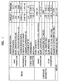
- FIG. 1 shows an example of a property value of an exposure apparatus concerning the present embodiment, a mask used in said exposure apparatus and a resist exposed by the mask.
- heat parameters such as density, heat capacity and heat conductance, mechanical parameters, such as Young's modulus, coefficient of linear thermal expansion and Poisson's ratio, and structure parameters, such as thickness and width. Consequently, as an example, the above parameters of silicon and diamond that are leading materials for the membrane now are shown in FIG. 1.
- the material is not limited in the present invention, further preferable material can be used, however the case of adopting silicon and diamond is explained for an example in the present embodiment.
- beam parameters half maximum at full width
- beam current and acceleration voltage such as scan length V, scan width H, interval of scan lines P and overjumped lines are shown.
- FIG. 2 is a view for explaining a conventional method of an electron beam scanning.
- a plurality of scan lines SL1 to SLn stretching in x direction and lining in certain intervals in y direction in the view are set.
- the length of horizontal scanning in x direction is defined as scan width H that corresponds to the length of the scan line
- the length of vertical scan length in y direction is defined as scan length V in the view.
- the interval of scan lines P is widened and illustrated, however, the interval of scan lines P is, for example, actually about 10 ⁇ m as shown in FIG. 1. Since the beam diameter (half maximum at full width) is about 1 mm (refer to FIG. 1), the beam diameter is about 100 times the interval of scan lines and greatly wide. The interval of scan lines is very narrow for the beam diameter as mentioned above to resolve variation of the beam and to improve the position accuracy of the pattern projected to the resist by scanning finely with an electron beam. Moreover, as mentioned later, in exposure by an electron beam, by changing irradiating angle of the electron beam by deflection, the pattern position projected to the resist can be corrected. Since a pattern formed in the membrane M is, for example, 50 nm to 60 nm, there is an advantage that the position correction of the pattern formed on the membrane M can be performed more finely when the interval of scan lines are made small.
- the electron beam is moved lower to the next scan line SL2, further the electron beam scans from right to left on the scan line SL2.
- the electron beam scans on the scan lines set in descending order and scans by turns to the bottom scan line SLn.
- the scanning speed is determined by the resist sensitivity.
- beam diameter is defined as 1 mm and interval of scan lines P is defined as 10 ⁇ m, 100 electron beams are overlapped at one membrane position.
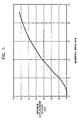
- FIG. 3 is a view showing a result analyzing the position in x direction in the middle portion of the membrane C and maximum displacement of the pattern by rise in temperature in the case of changing the membrane width L in x direction of the membrane M as shown in FIG. 2 to irradiate the electron beam to the resist by a conventional method of an electron beam scanning.
- silicon is used as a membrane material and membrane thickness is defined as 500 nm, beam diameter (half maximum at full width) is defined as 1 mm, beam current is defined as 5 pA, scan width (H) is defined as 25 mm, scan length (V) is defined as 25 mm, interval of scan lines (P) is defined as 10 ⁇ m and the resist sensitivity is defined as 1.6 ⁇ C/cm 2 .
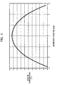
- FIG. 4 is a view showing the analysis result of the membrane position and rise in temperature in the case that the membrane material is diamond
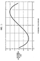
- FIG. 5 is a view showing the analysis result of the membrane position and maximum displacement of the pattern by the heat.
- FIG. 4 is the analysis result in the case that thickness of the membrane consisting of diamond is decided as 700 nm, the membrane width L is decided as 23 nm equal to the die size, that is to say a mask consisting of the one membrane having no beam, and the other condition is equal to the condition in FIG. 3.
- Diamond is regarded as the ideal material at the present time as a material having very large heat conductance and high mechanical rigidity.
- the heat conductance of diamond is 10 or more times higher than silicon as shown in FIG. 1.
- the pattern position is displaced up to ⁇ 20 nm as a result of rise in temperature of the membrane showing in FIG. 4.
- displacement of the pattern is 0 in the edge of the membrane fixed by the thick film portion, and displacement of the pattern is 0 in the middle portion since the patterns is expanded from side to side in x direction. Therefore, displacement of the pattern becomes the maximum at the center of the middle portion and the edge portion. That is to say, the middle portion and the edge portion become the fixed edges, the membrane is expanded greatly.
- the membrane width is decided as 23 mm in FIG. 4 and FIG. 5, however, this membrane width belongs to a small category as die width reduced-projected by an optical mask.
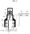
- FIG. 6 is a schematic block diagram of the exposure apparatus concerning the present embodiment.
- the exposure apparatus shown in FIG. 6 is an exposure apparatus applied to LEEPL technology.
- the exposure apparatus shown in FIG. 6 has an electron gun 101, a condenser lens 102, an aperture 103, a pair of main deflector 104a and 104b, a pair of sub deflector 105a and 105b, a scan line set means 106 and a deflection drive means 107.
- the electron gun 101 shoot an electron beam EB with an acceleration voltage of about 2 kV.
- the electron beam shot from the electron gun 101 converges to a parallel beam through the condenser lens 102.
- the unwanted portion of the electron beam EB converged to the parallel beam is shadowed by the aperture 103.
- the electron beam EB After the electron beam EB is swung to the target in which the electron beam EB is irradiated by the main deflector 104a, the electron beam EB is swung back to the direction parallel to the optical axis by the main deflector 104b. Hereby, the electron beam EB is irradiated almost vertically to the mask MA. Further, by the main deflector 104a and 104b, the electron beam EB scans on the target scan line SL.
- the sub deflector 105a and 105b control an incident angle of the electron beam EB to the mask MA to correct the pattern position projected on a wafer W.
- the sub deflector 105a and 105b control an incident angle of the electron beam EB to the mask MA to correct the pattern position projected on a wafer W.
- the pattern of the mask MA displacing from the accurate position is corrected to the accurate position on the wafer W and is projected.
- FIG. 6 by controlling an irradiating angle, the irradiating position of the electron beam EB to the wafer W is moved by ⁇ .
- the scan line set means 106 sets a plurality of scan lines that should be scanned by the electron beam on the mask MA.
- the deflection drive means 107 controls the main deflector 104a, 104b and the sub deflector 105a, 105b.
- the deflection drive means 107, the main deflector 104a, 104b and the sub deflector 105a, 105b correspond to a means of an electron beam scanning of the present invention.
- the interlaced-scanning. that the electron beam EB scans to jump over scan lines set by the scan line set means 106 by number of overjumped lines that can control rise in temperature of the mask MA, for details membrane M, by overlapping of the electron beam EB is performed. Further, by repeating the interlaced-scanning for the interlaced-scan lines, the electron beam EB scans on all set scan lines.
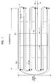
- FIG. 7 is a view for explaining an example of the interlaced-scanning performed in the exposure apparatus and the exposure method concerning to the present embodiment.
- number of the scan lines is thinned out rather than FIG .2, setting number of the scan lines SL and the interval of the set scan lines in itself are in a conventional manner. Moreover, in the case that the position of scan line is not made issue of especially, it is called simply as the scan line SL. For example, several thousand scan lines SL, for example about 4000, are set on the membrane M of the mask MA. However, setting number of scan lines SL may be changed as 2000 or 1000 of membrane size according to size of the membrane M.
- the scan lines SL are jumped over by k (number of overjumped lines)
- the electron beam is moved down to the scan line SL1+k and further the scan line SL1+k is scanned from right to left by the electron beam.
- the electron beam is made to jump over by k from top to bottom in the fixed direction, to scan on the scan line and to scan to the bottom scan line SL by turns.
- the scanning speed is determined by the resist sensitivity.
- the interlaced-scanning is repeated for the interlaced-scan lines SL.
- the electron beam is swung back to the second scan line SL2 from the top.
- the scan lines SL are jumped over by k, the electron beam is moved down to the scan line SL2+k and further the scan line SL2+k is scanned from right to left by the electron beam.
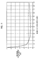
- FIG. 8 is a view showing the result of analyzing number of overjumped lines and maximum displacement of the pattern by the heat in the case of irradiating the electron beam to the mask by the electron beam interlaced-scanning as shown in FIG. 6.
- FIG. 8 is a view showing relationship of number of overjumped lines and displacement of the position of the middle portion of the membrane M in FIG. 7 in the case that the electron beam is made to interlaced-scan to the membrane M in the above condition.
- the scan width H and the scan length V are defined larger than the case of FIG. 3 to FIG. 5 by assuming the application of the mask consisting of the membrane with the beams.
- displacement of the pattern by the heat is reduced sharply with increase of number of overjumped lines, when number of overjumped lines is 50 to 70, displacement of the pattern becomes the minimum, afterward displacement of the pattern by the heat increases gently.
- Sharp reduction of displacement of the pattern by increase of number of overjumped lines is due to reduction of overlapping of the beams.
- number of overjumped lines is defined as 70 or more, displacement of the pattern increases by the heat, because the next interlaced-scanning starts before temperature of the membrane has fallen, since time required for single interlaced-scanning is reduced by increase of number of overjumped lines.
- the optimized value exists in number of overjumped lines, however, if it can be only optimized, displacement of the pattern by the heat can be reduced within an acceptable value even in the large membrane width that is difficult by the conventional method of an electron beam scanning.
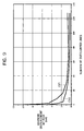
- FIG. 9 is a view of relationship number of scan lines and maximum displacement of the pattern by the heat in the case that diamond is adopted for the membrane material. Moreover, the other conditions are equivalent to the analysis in the case of silicon shown in FIG. 8. In FIG. 9, the case that the membrane width L is defined as 13 mm (shown as CV1 in the view) and the case that the membrane width is defined as 9 mm (shown as CV2 in the view) are shown.
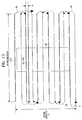
- FIG. 10 is a view for explaining the other example of the interlaced-scanning.
- FIG. 7 an example that the interlaced-scanning is performed by optimal number of overjumped lines k, however in the present example after the interlaced-scanning of the electron beam in the fixed direction by twice optimal number of overjumped lines k, the interlaced-scanning of the electron beam in opposite of said fixed direction is performed repeatedly.
- the scan lines SL are jumped over by 2k
- the electron beam is moved down to the scan line SL1+2k and further the scan line SL1+2k is scanned from right to left by the electron beam.
- the electron beam is made to jump over by 2k from top to bottom in the fixed direction, to scan on the scan line and to scan to the bottom scan line SL by turns.
- the scanning speed is determined by the resist sensitivity.
- the electron beam is moved optimal number of overjumped lines k up or down (FIG. 10 shows an example of making to move down) the interlaced-scanning that 2k scan lines SL are jumped over is performed from bottom to top in opposite to the above.
- the scan lines SL between the scan lines SL scanned in the previous interlaced-scanning are scanned.
- the membrane of large size can be adopted.
- the membrane width is about 13 mm or less (refer to CV1 in FIG. 9). Therefore, it is difficult to expose a die of size of about 26 mm x 33 mm by the mask consisting of a sheet of membrane.
- FIG. 11 is a view showing a first example of a preferred mask.
- horizontal size of dies I, II that are a target of exposure is defined as D
- vertical size is defined as E.
- a beam of thick film T sections to two main membrane M1, M2 and a portion corresponding to the beam T is defined as a sub membrane N1 to prepare for a mask.
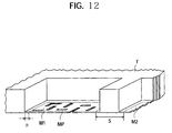
- FIG. 12 is a perspective view of principal portion of the main membrane M1. As shown in FIG. 12, in the main membrane M1 a margin is set between the main membrane M1 and the beam T, on the main membrane M1 a pattern MP composed of the aperture is formed. Between the main membrane M1 and the main membrane M2 the beam T is formed. The width S of the beam T shown in FIG. 11 contains the margin .
- the electron beam is made to interlaced-scan in the region including the main membrane M1, M2 and the sub membrane N1.
- the pattern of the main membrane M1, M2 is projected on the die I
- the pattern of the sub membrane N1 is projected on the die II.
- the region of the beam T that cannot be projected by the main membrane M1, M2 is projected by the sub membrane N1.
- H is the scan width.
- the mask of the above construction has large size membranes M1, M2, N1, however, by using the exposure devise and the exposure method concerning the present embodiment displacement of the pattern by the heat can be reduced. Moreover, since the scan width H is about 1.72 times the horizontal size of the die, the scan width H can be reduced.
- FIG. 13 is a view showing a second example of a preferred mask.
- the mask consisting of the minimum number (three) of the membranes that displacement of the pattern by the heat can be reduced to 1 nm or less was explained, however, by making the mask construction consisting of five membranes, silicon can be used as the membrane material.
- the width of the main membranes M1, M2, M3 are decided as W respectively, the width of the beam T is decided as S, the width of the sub membrane N1 becomes S.
- the point that the widths of the main membrane M1, M2, M3 are expanded as a margin and the width S of the beam T includes the margin is similar to the above.
- the magnification of the scan width H for the horizontal size of the die D becomes high, however the membrane composed of a silicon material of the membrane width of 6 mm that displacement of the pattern is confirmed to be controlled 1 nm or less by the interlaced-scanning can be adopted (refer to FIG. 8).
- the electron beam is made to interlaced-scan the region including the main membranes M1, M2, M3 and the sub membranes N1, N2.
- the die I the patterns of the main membranes M1, M2, M3 are projected
- the die II the patterns of the sub membranes N1, N2 are exposed.
- the region of the beam T that cannot be projected by the main membranes M1, M2, M3 is projected by the sub membranes N1 N2.
- the main membranes M1, M2 show two masks and the sub membrane N1 shows one mask
- the example shown in FIG 13 the main membranes M1, M2, M3 show three masks and the sub membranes N1, N2 show two masks, however, in a similar way number of the main membranes and the sub membranes can be increased.
- the scan width H is calculated to replace (W+S)/(2W+S) in the above equation by (2W+2S)/(3W+2S).
- the scan width H is reduced to about 1.5 times the horizontal size D in the case that number of the membranes is decided as the minimum, and if number of the membranes increases, the scan width H becomes less than twice the horizontal size of the die D even if number of membranes increases.
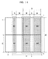
- FIG. 14 is a view showing a third example of a preferred mask.
- the mask shown in FIG. 14 is a mask that the vertical length of the main membranes M1, M2 and the sub membrane N1 shown in FIG. 11 are expanded to the adjacent die III, IV, further the main membranes M1', M2' and the sub membrane N1' are formed.
- the main membrane M1 and the main membrane M1', the main membrane M2 and the main membrane M2', the sub membrane N1 and the sub membrane N1' are not sectioned by the beams, they are respectively composed of one membrane.
- the electron beam is made to interlaced-scan the region including the main membranes M1, M2, M1', M2' and the sub membranes N1, N2.
- the wafer is moved by the horizontal size of the die D to expose the pattern of the sub membrane N1, further the wafer is moved by the vertical size of the die E to expose the sub membrane N1', and further the wafer is moved by the horizontal size of the die D to expose the patterns of the main membranes M1, M2.
- said mask can perform a complementary exposure.
- each membrane is about twice the membrane shown in FIG. 11, however, the horizontal size does not change. Since displacement of the pattern by the heat is affected by the square of the shorter size among the horizontal size and the vertical size of the membrane, there is no problem if the membrane is lengthen vertically like this. It is the same about the mechanical strength.
- the mask of the above constitution has the membrane of comparatively large size, however, by using for the exposure apparatus and the exposure method concerning the present embodiment, the mask has the effects that the complementary exposure can be performed, besides displacement of the pattern by the heat can be prevented.
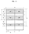
- FIG. 15 is a view showing a fourth example of a preferred mask.
- the mask is an example of a mask that the complementary exposure can be performed by a horizontally long membrane.
- the vertical size E of the dies I to IV that is an object of the exposure is divided into the vertical size W of two main membranes M1, M2 and the size S of the beam T sectioning the main membranes.
- the portion corresponding to the beam T is decided as the sub membrane N1 to prepare for the mask.
- the horizontal size of each membrane M1, M2, N1 is expanded, further the main membranes M1', M2', the sub membrane N1' are formed.
- the main membrane M1 and the main membrane M1', the main membrane M2 and the main membrane M2', the sub membrane N1 and the sub membrane N1' are not sectioned by the beam, they are constituted by one membrane respectively.
- the electron beam is made to interlaced-scanned the region including the main membranes M1, M2, M1', M2' or the sub membranes N1, N1'.
- the main membranes M1, M2 and the sub membrane N1 are exposed. That is to say, it is the mask that the complementary exposure can be performed.
- the scan width of the mask shown in FIG. 15 is calculated by replacing the horizontal size D of the above equation (1) by the vertical size E.
- the vertical size that is shorter size of the membrane is decided as 13 mm, in the similar way the mask that displacement of the pattern by the heat is small can be realized.
- the mask of the above constitution has the membrane of comparatively large size, however, by using for the exposure apparatus and the exposure method concerning the present embodiment, the mask has the effects that the complementary exposure can be performed, besides displacement of the pattern by the heat can be controlled.
- the exposure apparatus and the exposure method concerning the present embodiment explained in the above have the effects explained below.
- rise in temperature of the membrane can be controlled, displacement of the pattern formed in the membrane can be reduced the acceptable value or less without sacrificing throughput.
- the position accuracy of the projected pattern projected on the exposed object can be improved by using the mask that the pattern is formed in the membrane.
- the membrane of large size can be adopted and the mask with the beam of simple constitution can be used.
- the conventional mask as described in Japanese Unexamined Patent Publication No. 2003-59819 can be used.
- the exposure apparatus and the exposure method concerning the present embodiment are applied preferably to the production of the semiconductor devices that the position accuracy of the pattern required is especially high.
- the circuit pattern is formed.
- a semiconductor integrated circuit is formed.
- the present invention is not limited to the above explanation of the embodiments.
- an example of the electron beam is explained, however, except for the electron beam, a charged particle beam such as an ion beam and so on can be applied in a similar way.
- a charged particle beam such as an ion beam and so on
- an example that the mask that the pattern is formed by the aperture on the membrane is also explained, however a mask that the pattern of a scatterer is formed on the membrane can be used. Because in the mask that the membrane is adopted, in a similar way, displacement of the pattern by the heat occurs easily.
Landscapes
- Engineering & Computer Science (AREA)
- Chemical & Material Sciences (AREA)
- Nanotechnology (AREA)
- Physics & Mathematics (AREA)
- Crystallography & Structural Chemistry (AREA)
- General Physics & Mathematics (AREA)
- Health & Medical Sciences (AREA)
- Mathematical Physics (AREA)
- Theoretical Computer Science (AREA)
- Manufacturing & Machinery (AREA)
- Condensed Matter Physics & Semiconductors (AREA)
- Analytical Chemistry (AREA)
- Toxicology (AREA)
- Life Sciences & Earth Sciences (AREA)
- Environmental & Geological Engineering (AREA)
- Atmospheric Sciences (AREA)
- Public Health (AREA)
- Epidemiology (AREA)
- Electron Beam Exposure (AREA)
- Exposure And Positioning Against Photoresist Photosensitive Materials (AREA)
Applications Claiming Priority (2)
| Application Number | Priority Date | Filing Date | Title |
|---|---|---|---|
| JP2003420685A JP2005183577A (ja) | 2003-12-18 | 2003-12-18 | 露光装置、露光方法、および半導体装置の製造方法 |
| JP2003420685 | 2003-12-18 |
Publications (2)
| Publication Number | Publication Date |
|---|---|
| EP1544895A2 true EP1544895A2 (de) | 2005-06-22 |
| EP1544895A3 EP1544895A3 (de) | 2007-01-17 |
Family
ID=34510661
Family Applications (1)
| Application Number | Title | Priority Date | Filing Date |
|---|---|---|---|
| EP04029803A Withdrawn EP1544895A3 (de) | 2003-12-18 | 2004-12-15 | Belichtungsgerät, Belichtungsverfahren und Verfahren zur Herstellung von Halbleitern |
Country Status (5)
| Country | Link |
|---|---|
| US (1) | US7326940B2 (de) |
| EP (1) | EP1544895A3 (de) |
| JP (1) | JP2005183577A (de) |
| KR (1) | KR20050061383A (de) |
| TW (1) | TWI267128B (de) |
Cited By (1)
| Publication number | Priority date | Publication date | Assignee | Title |
|---|---|---|---|---|
| CN103093851A (zh) * | 2013-01-21 | 2013-05-08 | 江苏达胜加速器制造有限公司 | 电子束流大小的导向控制装置 |
Families Citing this family (4)
| Publication number | Priority date | Publication date | Assignee | Title |
|---|---|---|---|---|
| JP5701201B2 (ja) * | 2011-12-19 | 2015-04-15 | 株式会社Sen | イオン注入方法及びイオン注入装置 |
| JP2017063101A (ja) | 2015-09-24 | 2017-03-30 | 株式会社アドバンテスト | 露光装置および露光方法 |
| US10446367B2 (en) * | 2018-03-07 | 2019-10-15 | Kla-Tencor Corporation | Scan strategies to minimize charging effects and radiation damage of charged particle beam metrology system |
| US12191110B2 (en) * | 2021-04-20 | 2025-01-07 | The University Of Liverpool | Reduced spatial/temporal overlaps to increase temporal overlaps to increase precision in focused ion beam FIB instruments for milling and imaging and focused ion beams for lithography |
Family Cites Families (16)
| Publication number | Priority date | Publication date | Assignee | Title |
|---|---|---|---|---|
| DE2837590A1 (de) | 1978-08-29 | 1980-03-13 | Ibm Deutschland | Verfahren zur schattenwurfbelichtung |
| JP2837743B2 (ja) * | 1990-06-27 | 1998-12-16 | 富士通株式会社 | 荷電粒子ビーム露光方法およびそれに用いるステンシルマスク |
| DE69206425T2 (de) * | 1991-01-11 | 1996-05-02 | Fujitsu Ltd | Belichtungsvorrichtung mit Strahlen aus geladenen Teilchen zur Verbesserung des Heizzustandes einer Blockmaske. |
| JP3689949B2 (ja) * | 1995-12-19 | 2005-08-31 | 株式会社ニコン | 投影露光装置、及び該投影露光装置を用いたパターン形成方法 |
| US5847959A (en) | 1997-01-28 | 1998-12-08 | Etec Systems, Inc. | Method and apparatus for run-time correction of proximity effects in pattern generation |
| US5831272A (en) | 1997-10-21 | 1998-11-03 | Utsumi; Takao | Low energy electron beam lithography |
| JP2000003847A (ja) * | 1998-06-15 | 2000-01-07 | Canon Inc | 荷電粒子線縮小転写装置及びデバイス製造方法 |
| US20020084429A1 (en) * | 2000-10-17 | 2002-07-04 | Craighead Harold G. | Electron-beam patterning of functionalized self-assembled monolayers |
| US6724002B2 (en) * | 2001-01-31 | 2004-04-20 | Applied Materials, Inc. | Multiple electron beam lithography system with multiple beam modulated laser illumination |
| JP3674573B2 (ja) | 2001-06-08 | 2005-07-20 | ソニー株式会社 | マスクおよびその製造方法と半導体装置の製造方法 |
| DE10295596T1 (de) * | 2001-11-12 | 2003-12-24 | Sony Corp | Komplementäre Masken und Verfahren zum Herstellen derselben, Belichtungsverfahren und Halbleiterbauteil sowie Verfahren zum Herstellen desselben |
| TWI229241B (en) * | 2001-12-04 | 2005-03-11 | Sony Corp | Mask and its manufacturing method, and manufacturing method of semiconductor device |
| JP3675421B2 (ja) * | 2002-03-28 | 2005-07-27 | ソニー株式会社 | マスクパターン補正方法、マスク製造方法、マスクおよび半導体装置の製造方法 |
| TWI278721B (en) * | 2002-04-09 | 2007-04-11 | Nikon Corp | Exposure method, exposure apparatus, and manufacturing method of device |
| JP2004207385A (ja) * | 2002-12-24 | 2004-07-22 | Rohm Co Ltd | マスク、その製造方法およびこれを用いた半導体装置の製造方法 |
| JP4738723B2 (ja) * | 2003-08-06 | 2011-08-03 | キヤノン株式会社 | マルチ荷電粒子線描画装置、荷電粒子線の電流の測定方法及びデバイス製造方法 |
-
2003
- 2003-12-18 JP JP2003420685A patent/JP2005183577A/ja active Pending
-
2004
- 2004-12-03 US US11/003,968 patent/US7326940B2/en not_active Expired - Fee Related
- 2004-12-15 EP EP04029803A patent/EP1544895A3/de not_active Withdrawn
- 2004-12-17 TW TW093139259A patent/TWI267128B/zh active
- 2004-12-17 KR KR1020040107542A patent/KR20050061383A/ko not_active Ceased
Cited By (1)
| Publication number | Priority date | Publication date | Assignee | Title |
|---|---|---|---|---|
| CN103093851A (zh) * | 2013-01-21 | 2013-05-08 | 江苏达胜加速器制造有限公司 | 电子束流大小的导向控制装置 |
Also Published As
| Publication number | Publication date |
|---|---|
| US7326940B2 (en) | 2008-02-05 |
| KR20050061383A (ko) | 2005-06-22 |
| TW200532387A (en) | 2005-10-01 |
| JP2005183577A (ja) | 2005-07-07 |
| EP1544895A3 (de) | 2007-01-17 |
| US20050133734A1 (en) | 2005-06-23 |
| TWI267128B (en) | 2006-11-21 |
Similar Documents
| Publication | Publication Date | Title |
|---|---|---|
| KR100807957B1 (ko) | 빔 조사량 연산 방법, 묘화 방법, 기록 매체 및 묘화 장치 | |
| US7800084B2 (en) | System and method for charged-particle beam lithography | |
| JP2680074B2 (ja) | 荷電粒子ビーム露光を用いた半導体装置の製造方法 | |
| US5399872A (en) | Charged-particle beam exposure method | |
| EP0038808B1 (de) | Ionenstrahllithographie-verfahren und -gerät, die eine schritt - und wiederhol-belichtung benützen | |
| US4743766A (en) | Method of drawing a desired pattern on a target through exposure thereof with an electron beam | |
| JP3212360B2 (ja) | マスクの製造方法、および半導体集積回路装置の製造方法 | |
| US8461555B2 (en) | Charged particle beam writing method and charged particle beam writing apparatus | |
| US20040011966A1 (en) | Energy beam exposure method and exposure apparatus | |
| JP2007115999A (ja) | キャラクタプロジェクション(cp)方式の荷電粒子ビーム露光方法、キャラクタプロジェクション方式の荷電粒子ビーム露光装置及びプログラム | |
| JP2019144109A (ja) | 荷電粒子ビーム検査方法 | |
| JP4603305B2 (ja) | 露光方法、パターン寸法調整方法及び焦点ぼかし量取得方法 | |
| KR100281846B1 (ko) | 하전입자빔노광방법및그노광장치 | |
| JP3552344B2 (ja) | 荷電粒子線によるパターン転写方法および転写装置 | |
| EP1544895A2 (de) | Belichtungsgerät, Belichtungsverfahren und Verfahren zur Herstellung von Halbleitern | |
| KR20010051381A (ko) | 부분 일괄 전사 노광용 마스크 데이터 작성 방법, 및 노광방법 | |
| JP3080006B2 (ja) | 電子ビーム露光補正方法 | |
| US6352802B1 (en) | Mask for electron beam exposure and method of manufacturing semiconductor device using the same | |
| JPH10106931A (ja) | 電子ビーム露光方法およびそれを用いた半導体集積回路装置の製造方法 | |
| EP0153864A2 (de) | Elektronenstrahl-Belichtungsverfahren | |
| US6277531B1 (en) | Charged-particle-beam microlithography apparatus and methods including focal-point correction | |
| US6211528B1 (en) | Electron beam drawing method in which cell projection manner and variably shaped beam manner are used in combination | |
| JP2000195781A (ja) | 電子ビ―ム露光装置用ブロックマスクの作成方法及びブロックマスク | |
| US20260066219A1 (en) | Charged particle beam writing method, charged particle beam writing apparatus, and non-transitory computer-readable storage medium storing a program | |
| US20020036272A1 (en) | Charged-particle-beam microlithography methods and apparatus providing reduced reticle heating |
Legal Events
| Date | Code | Title | Description |
|---|---|---|---|
| PUAI | Public reference made under article 153(3) epc to a published international application that has entered the european phase |
Free format text: ORIGINAL CODE: 0009012 |
|
| AK | Designated contracting states |
Kind code of ref document: A2 Designated state(s): AT BE BG CH CY CZ DE DK EE ES FI FR GB GR HU IE IS IT LI LT LU MC NL PL PT RO SE SI SK TR |
|
| AX | Request for extension of the european patent |
Extension state: AL BA HR LV MK YU |
|
| PUAL | Search report despatched |
Free format text: ORIGINAL CODE: 0009013 |
|
| AK | Designated contracting states |
Kind code of ref document: A3 Designated state(s): AT BE BG CH CY CZ DE DK EE ES FI FR GB GR HU IE IS IT LI LT LU MC NL PL PT RO SE SI SK TR |
|
| AX | Request for extension of the european patent |
Extension state: AL BA HR LV MK YU |
|
| 17P | Request for examination filed |
Effective date: 20070702 |
|
| AKX | Designation fees paid |
Designated state(s): DE FR NL |
|
| STAA | Information on the status of an ep patent application or granted ep patent |
Free format text: STATUS: THE APPLICATION HAS BEEN WITHDRAWN |
|
| 18W | Application withdrawn |
Effective date: 20120322 |