EP1544164B1 - Assemblage hermétique à l'échelle de la plaquette pour dispositifs MEMS avec métallurgie à basse température - Google Patents
Assemblage hermétique à l'échelle de la plaquette pour dispositifs MEMS avec métallurgie à basse température Download PDFInfo
- Publication number
- EP1544164B1 EP1544164B1 EP04106449.4A EP04106449A EP1544164B1 EP 1544164 B1 EP1544164 B1 EP 1544164B1 EP 04106449 A EP04106449 A EP 04106449A EP 1544164 B1 EP1544164 B1 EP 1544164B1
- Authority
- EP
- European Patent Office
- Prior art keywords
- free
- electroless
- tin
- nickel
- indium
- Prior art date
- Legal status (The legal status is an assumption and is not a legal conclusion. Google has not performed a legal analysis and makes no representation as to the accuracy of the status listed.)
- Expired - Lifetime
Links
- 238000004806 packaging method and process Methods 0.000 title description 17
- 238000005272 metallurgy Methods 0.000 title description 2
- PXHVJJICTQNCMI-UHFFFAOYSA-N Nickel Chemical compound [Ni] PXHVJJICTQNCMI-UHFFFAOYSA-N 0.000 claims description 434
- 229910052751 metal Inorganic materials 0.000 claims description 241
- 239000002184 metal Substances 0.000 claims description 239
- 229910052759 nickel Inorganic materials 0.000 claims description 208
- 229910000679 solder Inorganic materials 0.000 claims description 199
- 238000007772 electroless plating Methods 0.000 claims description 164
- ATJFFYVFTNAWJD-UHFFFAOYSA-N Tin Chemical compound [Sn] ATJFFYVFTNAWJD-UHFFFAOYSA-N 0.000 claims description 155
- 229910052718 tin Inorganic materials 0.000 claims description 155
- BASFCYQUMIYNBI-UHFFFAOYSA-N platinum Chemical compound [Pt] BASFCYQUMIYNBI-UHFFFAOYSA-N 0.000 claims description 150
- 238000000034 method Methods 0.000 claims description 146
- 229910052738 indium Inorganic materials 0.000 claims description 123
- APFVFJFRJDLVQX-UHFFFAOYSA-N indium atom Chemical compound [In] APFVFJFRJDLVQX-UHFFFAOYSA-N 0.000 claims description 118
- 229910052733 gallium Inorganic materials 0.000 claims description 89
- GYHNNYVSQQEPJS-UHFFFAOYSA-N Gallium Chemical compound [Ga] GYHNNYVSQQEPJS-UHFFFAOYSA-N 0.000 claims description 82
- 230000008569 process Effects 0.000 claims description 79
- KCXVZYZYPLLWCC-UHFFFAOYSA-N EDTA Chemical compound OC(=O)CN(CC(O)=O)CCN(CC(O)=O)CC(O)=O KCXVZYZYPLLWCC-UHFFFAOYSA-N 0.000 claims description 67
- 229910052697 platinum Inorganic materials 0.000 claims description 63
- 239000010949 copper Substances 0.000 claims description 62
- 239000011701 zinc Substances 0.000 claims description 53
- 238000004519 manufacturing process Methods 0.000 claims description 50
- QAOWNCQODCNURD-UHFFFAOYSA-N Sulfuric acid Chemical compound OS(O)(=O)=O QAOWNCQODCNURD-UHFFFAOYSA-N 0.000 claims description 48
- 239000010948 rhodium Substances 0.000 claims description 45
- ROSDSFDQCJNGOL-UHFFFAOYSA-N Dimethylamine Chemical compound CNC ROSDSFDQCJNGOL-UHFFFAOYSA-N 0.000 claims description 40
- 229910052782 aluminium Inorganic materials 0.000 claims description 37
- XAGFODPZIPBFFR-UHFFFAOYSA-N aluminium Chemical compound [Al] XAGFODPZIPBFFR-UHFFFAOYSA-N 0.000 claims description 37
- 229910052802 copper Inorganic materials 0.000 claims description 37
- 229910052703 rhodium Inorganic materials 0.000 claims description 37
- MHOVAHRLVXNVSD-UHFFFAOYSA-N rhodium atom Chemical compound [Rh] MHOVAHRLVXNVSD-UHFFFAOYSA-N 0.000 claims description 37
- UMGDCJDMYOKAJW-UHFFFAOYSA-N thiourea Chemical compound NC(N)=S UMGDCJDMYOKAJW-UHFFFAOYSA-N 0.000 claims description 37
- RYGMFSIKBFXOCR-UHFFFAOYSA-N Copper Chemical compound [Cu] RYGMFSIKBFXOCR-UHFFFAOYSA-N 0.000 claims description 36
- 229910018614 Ni(H2PO2)2 Inorganic materials 0.000 claims description 35
- 229910052725 zinc Inorganic materials 0.000 claims description 34
- 230000003064 anti-oxidating effect Effects 0.000 claims description 33
- 229910052797 bismuth Inorganic materials 0.000 claims description 33
- KRKNYBCHXYNGOX-UHFFFAOYSA-N citric acid Chemical compound OC(=O)CC(O)(C(O)=O)CC(O)=O KRKNYBCHXYNGOX-UHFFFAOYSA-N 0.000 claims description 33
- KJTLSVCANCCWHF-UHFFFAOYSA-N Ruthenium Chemical compound [Ru] KJTLSVCANCCWHF-UHFFFAOYSA-N 0.000 claims description 30
- 229910052707 ruthenium Inorganic materials 0.000 claims description 29
- 239000000460 chlorine Substances 0.000 claims description 28
- 229910000510 noble metal Inorganic materials 0.000 claims description 27
- 229910052801 chlorine Inorganic materials 0.000 claims description 25
- LGQLOGILCSXPEA-UHFFFAOYSA-L nickel sulfate Chemical compound [Ni+2].[O-]S([O-])(=O)=O LGQLOGILCSXPEA-UHFFFAOYSA-L 0.000 claims description 25
- XLYOFNOQVPJJNP-ZSJDYOACSA-N heavy water Substances [2H]O[2H] XLYOFNOQVPJJNP-ZSJDYOACSA-N 0.000 claims description 22
- 229910000363 nickel(II) sulfate Inorganic materials 0.000 claims description 20
- 229910000838 Al alloy Inorganic materials 0.000 claims description 17
- ZAMOUSCENKQFHK-UHFFFAOYSA-N Chlorine atom Chemical compound [Cl] ZAMOUSCENKQFHK-UHFFFAOYSA-N 0.000 claims description 17
- 229910000375 tin(II) sulfate Inorganic materials 0.000 claims description 15
- XSQUKJJJFZCRTK-UHFFFAOYSA-N Urea Natural products NC(N)=O XSQUKJJJFZCRTK-UHFFFAOYSA-N 0.000 claims description 14
- AFVFQIVMOAPDHO-UHFFFAOYSA-N Methanesulfonic acid Chemical compound CS(O)(=O)=O AFVFQIVMOAPDHO-UHFFFAOYSA-N 0.000 claims description 13
- MGFYIUFZLHCRTH-UHFFFAOYSA-N nitrilotriacetic acid Chemical compound OC(=O)CN(CC(O)=O)CC(O)=O MGFYIUFZLHCRTH-UHFFFAOYSA-N 0.000 claims description 12
- NBIIXXVUZAFLBC-UHFFFAOYSA-N Phosphoric acid Chemical compound OP(O)(O)=O NBIIXXVUZAFLBC-UHFFFAOYSA-N 0.000 claims description 11
- FEWJPZIEWOKRBE-UHFFFAOYSA-N Tartaric acid Natural products [H+].[H+].[O-]C(=O)C(O)C(O)C([O-])=O FEWJPZIEWOKRBE-UHFFFAOYSA-N 0.000 claims description 11
- 239000011975 tartaric acid Substances 0.000 claims description 11
- 235000002906 tartaric acid Nutrition 0.000 claims description 11
- 239000008139 complexing agent Substances 0.000 claims description 10
- 150000001875 compounds Chemical class 0.000 claims description 9
- RCIVOBGSMSSVTR-UHFFFAOYSA-L stannous sulfate Chemical compound [SnH2+2].[O-]S([O-])(=O)=O RCIVOBGSMSSVTR-UHFFFAOYSA-L 0.000 claims description 9
- XUIMIQQOPSSXEZ-UHFFFAOYSA-N Silicon Chemical compound [Si] XUIMIQQOPSSXEZ-UHFFFAOYSA-N 0.000 claims description 8
- RILZRCJGXSFXNE-UHFFFAOYSA-N 2-[4-(trifluoromethoxy)phenyl]ethanol Chemical compound OCCC1=CC=C(OC(F)(F)F)C=C1 RILZRCJGXSFXNE-UHFFFAOYSA-N 0.000 claims description 7
- 229910052710 silicon Inorganic materials 0.000 claims description 7
- 239000010703 silicon Substances 0.000 claims description 7
- 239000010936 titanium Substances 0.000 claims description 7
- 229910052719 titanium Inorganic materials 0.000 claims description 7
- GSEJCLTVZPLZKY-UHFFFAOYSA-N Triethanolamine Chemical compound OCCN(CCO)CCO GSEJCLTVZPLZKY-UHFFFAOYSA-N 0.000 claims description 6
- 229960004418 trolamine Drugs 0.000 claims description 6
- FEWJPZIEWOKRBE-JCYAYHJZSA-N Dextrotartaric acid Chemical compound OC(=O)[C@H](O)[C@@H](O)C(O)=O FEWJPZIEWOKRBE-JCYAYHJZSA-N 0.000 claims description 5
- RHZWSUVWRRXEJF-UHFFFAOYSA-N indium tin Chemical compound [In].[Sn] RHZWSUVWRRXEJF-UHFFFAOYSA-N 0.000 claims description 5
- 229940098779 methanesulfonic acid Drugs 0.000 claims description 5
- RTAQQCXQSZGOHL-UHFFFAOYSA-N Titanium Chemical compound [Ti] RTAQQCXQSZGOHL-UHFFFAOYSA-N 0.000 claims description 4
- 229910000147 aluminium phosphate Inorganic materials 0.000 claims description 4
- NWAIGJYBQQYSPW-UHFFFAOYSA-N azanylidyneindigane Chemical compound [In]#N NWAIGJYBQQYSPW-UHFFFAOYSA-N 0.000 claims description 4
- VUAQKPWIIMBHEK-UHFFFAOYSA-K bis(methylsulfonyloxy)indiganyl methanesulfonate Chemical compound [In+3].CS([O-])(=O)=O.CS([O-])(=O)=O.CS([O-])(=O)=O VUAQKPWIIMBHEK-UHFFFAOYSA-K 0.000 claims description 4
- GZCWPZJOEIAXRU-UHFFFAOYSA-N tin zinc Chemical compound [Zn].[Sn] GZCWPZJOEIAXRU-UHFFFAOYSA-N 0.000 claims description 4
- LSNNMFCWUKXFEE-UHFFFAOYSA-M Bisulfite Chemical compound OS([O-])=O LSNNMFCWUKXFEE-UHFFFAOYSA-M 0.000 claims description 3
- QCEUXSAXTBNJGO-UHFFFAOYSA-N [Ag].[Sn] Chemical compound [Ag].[Sn] QCEUXSAXTBNJGO-UHFFFAOYSA-N 0.000 claims description 3
- RRXGIIMOBNNXDK-UHFFFAOYSA-N [Mg].[Sn] Chemical compound [Mg].[Sn] RRXGIIMOBNNXDK-UHFFFAOYSA-N 0.000 claims description 3
- MPZNMEBSWMRGFG-UHFFFAOYSA-N bismuth indium Chemical compound [In].[Bi] MPZNMEBSWMRGFG-UHFFFAOYSA-N 0.000 claims description 3
- JWVAUCBYEDDGAD-UHFFFAOYSA-N bismuth tin Chemical compound [Sn].[Bi] JWVAUCBYEDDGAD-UHFFFAOYSA-N 0.000 claims description 3
- KUNSUQLRTQLHQQ-UHFFFAOYSA-N copper tin Chemical compound [Cu].[Sn] KUNSUQLRTQLHQQ-UHFFFAOYSA-N 0.000 claims description 3
- YZZNJYQZJKSEER-UHFFFAOYSA-N gallium tin Chemical compound [Ga].[Sn] YZZNJYQZJKSEER-UHFFFAOYSA-N 0.000 claims description 3
- YZASAXHKAQYPEH-UHFFFAOYSA-N indium silver Chemical compound [Ag].[In] YZASAXHKAQYPEH-UHFFFAOYSA-N 0.000 claims description 3
- NJWNEWQMQCGRDO-UHFFFAOYSA-N indium zinc Chemical compound [Zn].[In] NJWNEWQMQCGRDO-UHFFFAOYSA-N 0.000 claims description 3
- WFKWXMTUELFFGS-UHFFFAOYSA-N tungsten Chemical compound [W] WFKWXMTUELFFGS-UHFFFAOYSA-N 0.000 claims description 3
- 229910052721 tungsten Inorganic materials 0.000 claims description 3
- 239000010937 tungsten Substances 0.000 claims description 3
- 229910052783 alkali metal Inorganic materials 0.000 claims description 2
- 150000001340 alkali metals Chemical class 0.000 claims description 2
- 229910000337 indium(III) sulfate Inorganic materials 0.000 claims description 2
- XGCKLPDYTQRDTR-UHFFFAOYSA-H indium(iii) sulfate Chemical compound [In+3].[In+3].[O-]S([O-])(=O)=O.[O-]S([O-])(=O)=O.[O-]S([O-])(=O)=O XGCKLPDYTQRDTR-UHFFFAOYSA-H 0.000 claims description 2
- 239000003795 chemical substances by application Substances 0.000 claims 2
- 239000000243 solution Substances 0.000 description 206
- 238000010587 phase diagram Methods 0.000 description 195
- 238000007747 plating Methods 0.000 description 187
- 235000012431 wafers Nutrition 0.000 description 186
- 239000010410 layer Substances 0.000 description 159
- 239000000203 mixture Substances 0.000 description 64
- 229910001092 metal group alloy Inorganic materials 0.000 description 62
- -1 Ni2+ ions Chemical class 0.000 description 61
- 229910045601 alloy Inorganic materials 0.000 description 61
- 239000000956 alloy Substances 0.000 description 61
- 238000007254 oxidation reaction Methods 0.000 description 61
- OAKJQQAXSVQMHS-UHFFFAOYSA-N Hydrazine Chemical compound NN OAKJQQAXSVQMHS-UHFFFAOYSA-N 0.000 description 52
- 238000007654 immersion Methods 0.000 description 47
- 238000005476 soldering Methods 0.000 description 47
- 231100000647 material safety data sheet Toxicity 0.000 description 39
- 230000003647 oxidation Effects 0.000 description 39
- 230000015572 biosynthetic process Effects 0.000 description 38
- KDLHZDBZIXYQEI-UHFFFAOYSA-N Palladium Chemical compound [Pd] KDLHZDBZIXYQEI-UHFFFAOYSA-N 0.000 description 37
- HEMHJVSKTPXQMS-UHFFFAOYSA-M Sodium hydroxide Chemical compound [OH-].[Na+] HEMHJVSKTPXQMS-UHFFFAOYSA-M 0.000 description 36
- 239000011777 magnesium Substances 0.000 description 36
- 239000011734 sodium Substances 0.000 description 36
- 229910002056 binary alloy Inorganic materials 0.000 description 34
- 150000002739 metals Chemical class 0.000 description 33
- HCHKCACWOHOZIP-UHFFFAOYSA-N Zinc Chemical compound [Zn] HCHKCACWOHOZIP-UHFFFAOYSA-N 0.000 description 32
- 229910052709 silver Inorganic materials 0.000 description 32
- VHUUQVKOLVNVRT-UHFFFAOYSA-N Ammonium hydroxide Chemical compound [NH4+].[OH-] VHUUQVKOLVNVRT-UHFFFAOYSA-N 0.000 description 31
- 239000004332 silver Substances 0.000 description 31
- 229910052708 sodium Inorganic materials 0.000 description 31
- BQCADISMDOOEFD-UHFFFAOYSA-N Silver Chemical compound [Ag] BQCADISMDOOEFD-UHFFFAOYSA-N 0.000 description 30
- 238000006073 displacement reaction Methods 0.000 description 30
- XLYOFNOQVPJJNP-UHFFFAOYSA-N water Chemical compound O XLYOFNOQVPJJNP-UHFFFAOYSA-N 0.000 description 30
- VEQPNABPJHWNSG-UHFFFAOYSA-N Nickel(2+) Chemical compound [Ni+2] VEQPNABPJHWNSG-UHFFFAOYSA-N 0.000 description 29
- JCXGWMGPZLAOME-UHFFFAOYSA-N bismuth atom Chemical compound [Bi] JCXGWMGPZLAOME-UHFFFAOYSA-N 0.000 description 29
- 238000006243 chemical reaction Methods 0.000 description 27
- 239000000126 substance Substances 0.000 description 27
- XXSPKSHUSWQAIZ-UHFFFAOYSA-L 36026-88-7 Chemical compound [Ni+2].[O-]P=O.[O-]P=O XXSPKSHUSWQAIZ-UHFFFAOYSA-L 0.000 description 26
- DGAQECJNVWCQMB-PUAWFVPOSA-M Ilexoside XXIX Chemical compound C[C@@H]1CC[C@@]2(CC[C@@]3(C(=CC[C@H]4[C@]3(CC[C@@H]5[C@@]4(CC[C@@H](C5(C)C)OS(=O)(=O)[O-])C)C)[C@@H]2[C@]1(C)O)C)C(=O)O[C@H]6[C@@H]([C@H]([C@@H]([C@H](O6)CO)O)O)O.[Na+] DGAQECJNVWCQMB-PUAWFVPOSA-M 0.000 description 25
- RJTANRZEWTUVMA-UHFFFAOYSA-N boron;n-methylmethanamine Chemical compound [B].CNC RJTANRZEWTUVMA-UHFFFAOYSA-N 0.000 description 25
- 238000009713 electroplating Methods 0.000 description 25
- 229920000642 polymer Polymers 0.000 description 25
- 229910021626 Tin(II) chloride Inorganic materials 0.000 description 24
- 239000011133 lead Substances 0.000 description 24
- 239000000463 material Substances 0.000 description 24
- 238000010586 diagram Methods 0.000 description 23
- 238000006722 reduction reaction Methods 0.000 description 23
- 229910052732 germanium Inorganic materials 0.000 description 22
- 229910052749 magnesium Inorganic materials 0.000 description 22
- FYYHWMGAXLPEAU-UHFFFAOYSA-N Magnesium Chemical compound [Mg] FYYHWMGAXLPEAU-UHFFFAOYSA-N 0.000 description 21
- 238000005275 alloying Methods 0.000 description 21
- 229940091250 magnesium supplement Drugs 0.000 description 21
- 238000005516 engineering process Methods 0.000 description 20
- 239000002253 acid Substances 0.000 description 19
- 239000004411 aluminium Substances 0.000 description 19
- 238000000151 deposition Methods 0.000 description 19
- 239000010931 gold Substances 0.000 description 19
- 150000002500 ions Chemical class 0.000 description 19
- 230000009467 reduction Effects 0.000 description 19
- 238000005260 corrosion Methods 0.000 description 18
- 230000007797 corrosion Effects 0.000 description 18
- GNPVGFCGXDBREM-UHFFFAOYSA-N germanium atom Chemical compound [Ge] GNPVGFCGXDBREM-UHFFFAOYSA-N 0.000 description 18
- VEXZGXHMUGYJMC-UHFFFAOYSA-N Hydrochloric acid Chemical compound Cl VEXZGXHMUGYJMC-UHFFFAOYSA-N 0.000 description 17
- 239000000908 ammonium hydroxide Substances 0.000 description 17
- 230000008021 deposition Effects 0.000 description 17
- 239000000758 substrate Substances 0.000 description 17
- 229910000905 alloy phase Inorganic materials 0.000 description 16
- 230000008018 melting Effects 0.000 description 16
- 238000002844 melting Methods 0.000 description 16
- 229910052763 palladium Inorganic materials 0.000 description 16
- 239000006227 byproduct Substances 0.000 description 15
- PCHJSUWPFVWCPO-UHFFFAOYSA-N gold Chemical compound [Au] PCHJSUWPFVWCPO-UHFFFAOYSA-N 0.000 description 15
- 229910020836 Sn-Ag Inorganic materials 0.000 description 14
- 229910020988 Sn—Ag Inorganic materials 0.000 description 14
- 229910052737 gold Inorganic materials 0.000 description 14
- 229910052739 hydrogen Inorganic materials 0.000 description 14
- 239000001257 hydrogen Substances 0.000 description 14
- 230000002459 sustained effect Effects 0.000 description 14
- YONPGGFAJWQGJC-UHFFFAOYSA-K titanium(iii) chloride Chemical compound Cl[Ti](Cl)Cl YONPGGFAJWQGJC-UHFFFAOYSA-K 0.000 description 14
- TXUICONDJPYNPY-UHFFFAOYSA-N (1,10,13-trimethyl-3-oxo-4,5,6,7,8,9,11,12,14,15,16,17-dodecahydrocyclopenta[a]phenanthren-17-yl) heptanoate Chemical compound C1CC2CC(=O)C=C(C)C2(C)C2C1C1CCC(OC(=O)CCCCCC)C1(C)CC2 TXUICONDJPYNPY-UHFFFAOYSA-N 0.000 description 13
- KWSLGOVYXMQPPX-UHFFFAOYSA-N 5-[3-(trifluoromethyl)phenyl]-2h-tetrazole Chemical compound FC(F)(F)C1=CC=CC(C2=NNN=N2)=C1 KWSLGOVYXMQPPX-UHFFFAOYSA-N 0.000 description 13
- 229960001484 edetic acid Drugs 0.000 description 13
- 229910001379 sodium hypophosphite Inorganic materials 0.000 description 13
- 239000001119 stannous chloride Substances 0.000 description 13
- 235000011150 stannous chloride Nutrition 0.000 description 13
- UFHFLCQGNIYNRP-UHFFFAOYSA-N Hydrogen Chemical compound [H][H] UFHFLCQGNIYNRP-UHFFFAOYSA-N 0.000 description 12
- 239000003513 alkali Substances 0.000 description 12
- 239000003638 chemical reducing agent Substances 0.000 description 12
- 229910020888 Sn-Cu Inorganic materials 0.000 description 11
- 229910020944 Sn-Mg Inorganic materials 0.000 description 11
- 229910020994 Sn-Zn Inorganic materials 0.000 description 11
- 229910019204 Sn—Cu Inorganic materials 0.000 description 11
- 229910009069 Sn—Zn Inorganic materials 0.000 description 11
- 239000000356 contaminant Substances 0.000 description 11
- 239000011521 glass Substances 0.000 description 11
- LONQOCRNVIZRSA-UHFFFAOYSA-L nickel(2+);sulfite Chemical compound [Ni+2].[O-]S([O-])=O LONQOCRNVIZRSA-UHFFFAOYSA-L 0.000 description 11
- MUBZPKHOEPUJKR-UHFFFAOYSA-N Oxalic acid Chemical compound OC(=O)C(O)=O MUBZPKHOEPUJKR-UHFFFAOYSA-N 0.000 description 10
- 229910020830 Sn-Bi Inorganic materials 0.000 description 10
- 229910018728 Sn—Bi Inorganic materials 0.000 description 10
- 239000002585 base Substances 0.000 description 10
- 238000007789 sealing Methods 0.000 description 10
- 239000001117 sulphuric acid Substances 0.000 description 10
- 235000011149 sulphuric acid Nutrition 0.000 description 10
- 229910018956 Sn—In Inorganic materials 0.000 description 9
- NINIDFKCEFEMDL-UHFFFAOYSA-N Sulfur Chemical compound [S] NINIDFKCEFEMDL-UHFFFAOYSA-N 0.000 description 9
- PHJJWPXKTFKKPD-UHFFFAOYSA-N [Ni+3].[O-]P([O-])[O-] Chemical compound [Ni+3].[O-]P([O-])[O-] PHJJWPXKTFKKPD-UHFFFAOYSA-N 0.000 description 9
- 239000007864 aqueous solution Substances 0.000 description 9
- 150000001768 cations Chemical class 0.000 description 9
- 230000001965 increasing effect Effects 0.000 description 9
- ACVYVLVWPXVTIT-UHFFFAOYSA-M phosphinate Chemical compound [O-][PH2]=O ACVYVLVWPXVTIT-UHFFFAOYSA-M 0.000 description 9
- 239000000047 product Substances 0.000 description 9
- 239000004065 semiconductor Substances 0.000 description 9
- 239000001509 sodium citrate Substances 0.000 description 9
- AXZWODMDQAVCJE-UHFFFAOYSA-L tin(II) chloride (anhydrous) Chemical compound [Cl-].[Cl-].[Sn+2] AXZWODMDQAVCJE-UHFFFAOYSA-L 0.000 description 9
- IKDUDTNKRLTJSI-UHFFFAOYSA-N hydrazine monohydrate Substances O.NN IKDUDTNKRLTJSI-UHFFFAOYSA-N 0.000 description 8
- 230000002829 reductive effect Effects 0.000 description 8
- 150000003467 sulfuric acid derivatives Chemical class 0.000 description 8
- 239000005864 Sulphur Substances 0.000 description 7
- 238000000909 electrodialysis Methods 0.000 description 7
- 230000008030 elimination Effects 0.000 description 7
- 238000003379 elimination reaction Methods 0.000 description 7
- PQTLYDQECILMMB-UHFFFAOYSA-L platinum(2+);sulfate Chemical compound [Pt+2].[O-]S([O-])(=O)=O PQTLYDQECILMMB-UHFFFAOYSA-L 0.000 description 7
- WSFSSNUMVMOOMR-UHFFFAOYSA-N Formaldehyde Chemical compound O=C WSFSSNUMVMOOMR-UHFFFAOYSA-N 0.000 description 6
- 238000009825 accumulation Methods 0.000 description 6
- 230000003197 catalytic effect Effects 0.000 description 6
- PSCMQHVBLHHWTO-UHFFFAOYSA-K indium(iii) chloride Chemical compound Cl[In](Cl)Cl PSCMQHVBLHHWTO-UHFFFAOYSA-K 0.000 description 6
- RODAKIFYLYKDTD-UHFFFAOYSA-N indium;sulfuric acid Chemical compound [In].OS(O)(=O)=O RODAKIFYLYKDTD-UHFFFAOYSA-N 0.000 description 6
- 239000012528 membrane Substances 0.000 description 6
- 150000002815 nickel Chemical class 0.000 description 6
- 229940053662 nickel sulfate Drugs 0.000 description 6
- 230000000737 periodic effect Effects 0.000 description 6
- 229910001415 sodium ion Inorganic materials 0.000 description 6
- LPXPTNMVRIOKMN-UHFFFAOYSA-M sodium nitrite Chemical compound [Na+].[O-]N=O LPXPTNMVRIOKMN-UHFFFAOYSA-M 0.000 description 6
- LSNNMFCWUKXFEE-UHFFFAOYSA-L sulfite Chemical compound [O-]S([O-])=O LSNNMFCWUKXFEE-UHFFFAOYSA-L 0.000 description 6
- 238000012876 topography Methods 0.000 description 6
- 230000002588 toxic effect Effects 0.000 description 6
- HRXKRNGNAMMEHJ-UHFFFAOYSA-K trisodium citrate Chemical compound [Na+].[Na+].[Na+].[O-]C(=O)CC(O)(CC([O-])=O)C([O-])=O HRXKRNGNAMMEHJ-UHFFFAOYSA-K 0.000 description 6
- 229940038773 trisodium citrate Drugs 0.000 description 6
- QTBSBXVTEAMEQO-UHFFFAOYSA-N Acetic acid Chemical compound CC(O)=O QTBSBXVTEAMEQO-UHFFFAOYSA-N 0.000 description 5
- 229910021205 NaH2PO2 Inorganic materials 0.000 description 5
- 229910021586 Nickel(II) chloride Inorganic materials 0.000 description 5
- 229910001128 Sn alloy Inorganic materials 0.000 description 5
- QAOWNCQODCNURD-UHFFFAOYSA-L Sulfate Chemical compound [O-]S([O-])(=O)=O QAOWNCQODCNURD-UHFFFAOYSA-L 0.000 description 5
- 229910010062 TiCl3 Inorganic materials 0.000 description 5
- 230000003247 decreasing effect Effects 0.000 description 5
- 238000005137 deposition process Methods 0.000 description 5
- 230000000694 effects Effects 0.000 description 5
- 238000003487 electrochemical reaction Methods 0.000 description 5
- 230000004927 fusion Effects 0.000 description 5
- 239000007789 gas Substances 0.000 description 5
- IXCSERBJSXMMFS-UHFFFAOYSA-N hydrogen chloride Substances Cl.Cl IXCSERBJSXMMFS-UHFFFAOYSA-N 0.000 description 5
- 238000005342 ion exchange Methods 0.000 description 5
- QMMRZOWCJAIUJA-UHFFFAOYSA-L nickel dichloride Chemical compound Cl[Ni]Cl QMMRZOWCJAIUJA-UHFFFAOYSA-L 0.000 description 5
- VLTRZXGMWDSKGL-UHFFFAOYSA-N perchloric acid Chemical compound OCl(=O)(=O)=O VLTRZXGMWDSKGL-UHFFFAOYSA-N 0.000 description 5
- 230000035699 permeability Effects 0.000 description 5
- AAIMUHANAAXZIF-UHFFFAOYSA-L platinum(2+);sulfite Chemical compound [Pt+2].[O-]S([O-])=O AAIMUHANAAXZIF-UHFFFAOYSA-L 0.000 description 5
- 239000002002 slurry Substances 0.000 description 5
- JBQYATWDVHIOAR-UHFFFAOYSA-N tellanylidenegermanium Chemical compound [Te]=[Ge] JBQYATWDVHIOAR-UHFFFAOYSA-N 0.000 description 5
- SDVHRXOTTYYKRY-UHFFFAOYSA-J tetrasodium;dioxido-oxo-phosphonato-$l^{5}-phosphane Chemical compound [Na+].[Na+].[Na+].[Na+].[O-]P([O-])(=O)P([O-])([O-])=O SDVHRXOTTYYKRY-UHFFFAOYSA-J 0.000 description 5
- 231100000331 toxic Toxicity 0.000 description 5
- 230000007306 turnover Effects 0.000 description 5
- NWZSZGALRFJKBT-KNIFDHDWSA-N (2s)-2,6-diaminohexanoic acid;(2s)-2-hydroxybutanedioic acid Chemical compound OC(=O)[C@@H](O)CC(O)=O.NCCCC[C@H](N)C(O)=O NWZSZGALRFJKBT-KNIFDHDWSA-N 0.000 description 4
- WHXSMMKQMYFTQS-UHFFFAOYSA-N Lithium Chemical compound [Li] WHXSMMKQMYFTQS-UHFFFAOYSA-N 0.000 description 4
- ATUOYWHBWRKTHZ-UHFFFAOYSA-N Propane Chemical compound CCC ATUOYWHBWRKTHZ-UHFFFAOYSA-N 0.000 description 4
- FAPWRFPIFSIZLT-UHFFFAOYSA-M Sodium chloride Chemical compound [Na+].[Cl-] FAPWRFPIFSIZLT-UHFFFAOYSA-M 0.000 description 4
- QVGXLLKOCUKJST-UHFFFAOYSA-N atomic oxygen Chemical compound [O] QVGXLLKOCUKJST-UHFFFAOYSA-N 0.000 description 4
- 230000008901 benefit Effects 0.000 description 4
- AXCZMVOFGPJBDE-UHFFFAOYSA-L calcium dihydroxide Chemical compound [OH-].[OH-].[Ca+2] AXCZMVOFGPJBDE-UHFFFAOYSA-L 0.000 description 4
- 239000000920 calcium hydroxide Substances 0.000 description 4
- 235000011116 calcium hydroxide Nutrition 0.000 description 4
- 229940095643 calcium hydroxide Drugs 0.000 description 4
- 229910001861 calcium hydroxide Inorganic materials 0.000 description 4
- 229910052799 carbon Inorganic materials 0.000 description 4
- 230000008859 change Effects 0.000 description 4
- KXZJHVJKXJLBKO-UHFFFAOYSA-N chembl1408157 Chemical compound N=1C2=CC=CC=C2C(C(=O)O)=CC=1C1=CC=C(O)C=C1 KXZJHVJKXJLBKO-UHFFFAOYSA-N 0.000 description 4
- 239000002131 composite material Substances 0.000 description 4
- 238000011109 contamination Methods 0.000 description 4
- BNIILDVGGAEEIG-UHFFFAOYSA-L disodium hydrogen phosphate Chemical compound [Na+].[Na+].OP([O-])([O-])=O BNIILDVGGAEEIG-UHFFFAOYSA-L 0.000 description 4
- 230000007613 environmental effect Effects 0.000 description 4
- 230000036541 health Effects 0.000 description 4
- 230000003993 interaction Effects 0.000 description 4
- LQBJWKCYZGMFEV-UHFFFAOYSA-N lead tin Chemical compound [Sn].[Pb] LQBJWKCYZGMFEV-UHFFFAOYSA-N 0.000 description 4
- 229910052744 lithium Inorganic materials 0.000 description 4
- 230000007246 mechanism Effects 0.000 description 4
- 229910052760 oxygen Inorganic materials 0.000 description 4
- 239000001301 oxygen Substances 0.000 description 4
- 238000000059 patterning Methods 0.000 description 4
- 230000001376 precipitating effect Effects 0.000 description 4
- 230000002265 prevention Effects 0.000 description 4
- 238000012545 processing Methods 0.000 description 4
- 238000000746 purification Methods 0.000 description 4
- 238000011160 research Methods 0.000 description 4
- YWFDDXXMOPZFFM-UHFFFAOYSA-H rhodium(3+);trisulfate Chemical compound [Rh+3].[Rh+3].[O-]S([O-])(=O)=O.[O-]S([O-])(=O)=O.[O-]S([O-])(=O)=O YWFDDXXMOPZFFM-UHFFFAOYSA-H 0.000 description 4
- DKNJHLHLMWHWOI-UHFFFAOYSA-L ruthenium(2+);sulfate Chemical compound [Ru+2].[O-]S([O-])(=O)=O DKNJHLHLMWHWOI-UHFFFAOYSA-L 0.000 description 4
- 150000003839 salts Chemical class 0.000 description 4
- 239000003381 stabilizer Substances 0.000 description 4
- 229910001174 tin-lead alloy Inorganic materials 0.000 description 4
- NCPXQVVMIXIKTN-UHFFFAOYSA-N trisodium;phosphite Chemical compound [Na+].[Na+].[Na+].[O-]P([O-])[O-] NCPXQVVMIXIKTN-UHFFFAOYSA-N 0.000 description 4
- 238000009736 wetting Methods 0.000 description 4
- UXVMQQNJUSDDNG-UHFFFAOYSA-L Calcium chloride Chemical compound [Cl-].[Cl-].[Ca+2] UXVMQQNJUSDDNG-UHFFFAOYSA-L 0.000 description 3
- 229910052686 Californium Inorganic materials 0.000 description 3
- 229910052684 Cerium Inorganic materials 0.000 description 3
- 229910052690 Einsteinium Inorganic materials 0.000 description 3
- 229910052693 Europium Inorganic materials 0.000 description 3
- 229910052764 Mendelevium Inorganic materials 0.000 description 3
- 229910052781 Neptunium Inorganic materials 0.000 description 3
- 229910052778 Plutonium Inorganic materials 0.000 description 3
- ZLMJMSJWJFRBEC-UHFFFAOYSA-N Potassium Chemical compound [K] ZLMJMSJWJFRBEC-UHFFFAOYSA-N 0.000 description 3
- KWYUFKZDYYNOTN-UHFFFAOYSA-M Potassium hydroxide Chemical compound [OH-].[K+] KWYUFKZDYYNOTN-UHFFFAOYSA-M 0.000 description 3
- 229910052777 Praseodymium Inorganic materials 0.000 description 3
- 229910052769 Ytterbium Inorganic materials 0.000 description 3
- 229910052787 antimony Inorganic materials 0.000 description 3
- WATWJIUSRGPENY-UHFFFAOYSA-N antimony atom Chemical compound [Sb] WATWJIUSRGPENY-UHFFFAOYSA-N 0.000 description 3
- 229910052785 arsenic Inorganic materials 0.000 description 3
- RQNWIZPPADIBDY-UHFFFAOYSA-N arsenic atom Chemical compound [As] RQNWIZPPADIBDY-UHFFFAOYSA-N 0.000 description 3
- 229910052789 astatine Inorganic materials 0.000 description 3
- RYXHOMYVWAEKHL-UHFFFAOYSA-N astatine atom Chemical compound [At] RYXHOMYVWAEKHL-UHFFFAOYSA-N 0.000 description 3
- 238000005844 autocatalytic reaction Methods 0.000 description 3
- 229910052788 barium Inorganic materials 0.000 description 3
- DSAJWYNOEDNPEQ-UHFFFAOYSA-N barium atom Chemical compound [Ba] DSAJWYNOEDNPEQ-UHFFFAOYSA-N 0.000 description 3
- 229910052793 cadmium Inorganic materials 0.000 description 3
- BDOSMKKIYDKNTQ-UHFFFAOYSA-N cadmium atom Chemical compound [Cd] BDOSMKKIYDKNTQ-UHFFFAOYSA-N 0.000 description 3
- 239000001110 calcium chloride Substances 0.000 description 3
- 229910001628 calcium chloride Inorganic materials 0.000 description 3
- HGLDOAKPQXAFKI-UHFFFAOYSA-N californium atom Chemical compound [Cf] HGLDOAKPQXAFKI-UHFFFAOYSA-N 0.000 description 3
- ZMIGMASIKSOYAM-UHFFFAOYSA-N cerium Chemical compound [Ce][Ce][Ce][Ce][Ce][Ce][Ce][Ce][Ce][Ce][Ce][Ce][Ce][Ce][Ce][Ce][Ce][Ce][Ce][Ce][Ce][Ce][Ce][Ce][Ce][Ce][Ce][Ce][Ce][Ce][Ce][Ce][Ce][Ce][Ce][Ce][Ce][Ce] ZMIGMASIKSOYAM-UHFFFAOYSA-N 0.000 description 3
- 230000007423 decrease Effects 0.000 description 3
- 238000006356 dehydrogenation reaction Methods 0.000 description 3
- CKBRQZNRCSJHFT-UHFFFAOYSA-N einsteinium atom Chemical compound [Es] CKBRQZNRCSJHFT-UHFFFAOYSA-N 0.000 description 3
- OGPBJKLSAFTDLK-UHFFFAOYSA-N europium atom Chemical compound [Eu] OGPBJKLSAFTDLK-UHFFFAOYSA-N 0.000 description 3
- 230000005496 eutectics Effects 0.000 description 3
- 230000004907 flux Effects 0.000 description 3
- 230000001939 inductive effect Effects 0.000 description 3
- XEEYBQQBJWHFJM-UHFFFAOYSA-N iron Substances [Fe] XEEYBQQBJWHFJM-UHFFFAOYSA-N 0.000 description 3
- 229910052746 lanthanum Inorganic materials 0.000 description 3
- FZLIPJUXYLNCLC-UHFFFAOYSA-N lanthanum atom Chemical compound [La] FZLIPJUXYLNCLC-UHFFFAOYSA-N 0.000 description 3
- HWSZZLVAJGOAAY-UHFFFAOYSA-L lead(II) chloride Chemical compound Cl[Pb]Cl HWSZZLVAJGOAAY-UHFFFAOYSA-L 0.000 description 3
- MQVSLOYRCXQRPM-UHFFFAOYSA-N mendelevium atom Chemical compound [Md] MQVSLOYRCXQRPM-UHFFFAOYSA-N 0.000 description 3
- LFNLGNPSGWYGGD-UHFFFAOYSA-N neptunium atom Chemical compound [Np] LFNLGNPSGWYGGD-UHFFFAOYSA-N 0.000 description 3
- 238000006386 neutralization reaction Methods 0.000 description 3
- 229910001453 nickel ion Inorganic materials 0.000 description 3
- MWUXSHHQAYIFBG-UHFFFAOYSA-N nitrogen oxide Inorganic materials O=[N] MWUXSHHQAYIFBG-UHFFFAOYSA-N 0.000 description 3
- ORQBXQOJMQIAOY-UHFFFAOYSA-N nobelium Chemical compound [No] ORQBXQOJMQIAOY-UHFFFAOYSA-N 0.000 description 3
- 235000006408 oxalic acid Nutrition 0.000 description 3
- 239000003002 pH adjusting agent Substances 0.000 description 3
- 229910052698 phosphorus Inorganic materials 0.000 description 3
- OYEHPCDNVJXUIW-UHFFFAOYSA-N plutonium atom Chemical compound [Pu] OYEHPCDNVJXUIW-UHFFFAOYSA-N 0.000 description 3
- 239000011591 potassium Substances 0.000 description 3
- 229910052700 potassium Inorganic materials 0.000 description 3
- 229960003975 potassium Drugs 0.000 description 3
- PUDIUYLPXJFUGB-UHFFFAOYSA-N praseodymium atom Chemical compound [Pr] PUDIUYLPXJFUGB-UHFFFAOYSA-N 0.000 description 3
- 230000001681 protective effect Effects 0.000 description 3
- 239000011241 protective layer Substances 0.000 description 3
- 230000002285 radioactive effect Effects 0.000 description 3
- 229910052705 radium Inorganic materials 0.000 description 3
- HCWPIIXVSYCSAN-UHFFFAOYSA-N radium atom Chemical compound [Ra] HCWPIIXVSYCSAN-UHFFFAOYSA-N 0.000 description 3
- 230000035939 shock Effects 0.000 description 3
- 125000004436 sodium atom Chemical group 0.000 description 3
- DZCAZXAJPZCSCU-UHFFFAOYSA-K sodium nitrilotriacetate Chemical compound [Na+].[Na+].[Na+].[O-]C(=O)CN(CC([O-])=O)CC([O-])=O DZCAZXAJPZCSCU-UHFFFAOYSA-K 0.000 description 3
- 230000006641 stabilisation Effects 0.000 description 3
- 238000011105 stabilization Methods 0.000 description 3
- 229910052712 strontium Inorganic materials 0.000 description 3
- CIOAGBVUUVVLOB-UHFFFAOYSA-N strontium atom Chemical compound [Sr] CIOAGBVUUVVLOB-UHFFFAOYSA-N 0.000 description 3
- 150000003460 sulfonic acids Chemical class 0.000 description 3
- 229910052714 tellurium Inorganic materials 0.000 description 3
- PORWMNRCUJJQNO-UHFFFAOYSA-N tellurium atom Chemical compound [Te] PORWMNRCUJJQNO-UHFFFAOYSA-N 0.000 description 3
- 229910052716 thallium Inorganic materials 0.000 description 3
- BKVIYDNLLOSFOA-UHFFFAOYSA-N thallium Chemical compound [Tl] BKVIYDNLLOSFOA-UHFFFAOYSA-N 0.000 description 3
- 230000009466 transformation Effects 0.000 description 3
- NAWDYIZEMPQZHO-UHFFFAOYSA-N ytterbium Chemical compound [Yb] NAWDYIZEMPQZHO-UHFFFAOYSA-N 0.000 description 3
- 229910001316 Ag alloy Inorganic materials 0.000 description 2
- OKTJSMMVPCPJKN-UHFFFAOYSA-N Carbon Chemical compound [C] OKTJSMMVPCPJKN-UHFFFAOYSA-N 0.000 description 2
- CURLTUGMZLYLDI-UHFFFAOYSA-N Carbon dioxide Chemical compound O=C=O CURLTUGMZLYLDI-UHFFFAOYSA-N 0.000 description 2
- VEXZGXHMUGYJMC-UHFFFAOYSA-M Chloride anion Chemical compound [Cl-] VEXZGXHMUGYJMC-UHFFFAOYSA-M 0.000 description 2
- KRHYYFGTRYWZRS-UHFFFAOYSA-N Fluorane Chemical compound F KRHYYFGTRYWZRS-UHFFFAOYSA-N 0.000 description 2
- 229910000927 Ge alloy Inorganic materials 0.000 description 2
- 229910003953 H3PO2 Inorganic materials 0.000 description 2
- 229910018104 Ni-P Inorganic materials 0.000 description 2
- GRYLNZFGIOXLOG-UHFFFAOYSA-N Nitric acid Chemical compound O[N+]([O-])=O GRYLNZFGIOXLOG-UHFFFAOYSA-N 0.000 description 2
- 229910018536 Ni—P Inorganic materials 0.000 description 2
- 229910020220 Pb—Sn Inorganic materials 0.000 description 2
- OAICVXFJPJFONN-UHFFFAOYSA-N Phosphorus Chemical compound [P] OAICVXFJPJFONN-UHFFFAOYSA-N 0.000 description 2
- WCUXLLCKKVVCTQ-UHFFFAOYSA-M Potassium chloride Chemical compound [Cl-].[K+] WCUXLLCKKVVCTQ-UHFFFAOYSA-M 0.000 description 2
- BUGBHKTXTAQXES-UHFFFAOYSA-N Selenium Chemical compound [Se] BUGBHKTXTAQXES-UHFFFAOYSA-N 0.000 description 2
- JHYLKGDXMUDNEO-UHFFFAOYSA-N [Mg].[In] Chemical compound [Mg].[In] JHYLKGDXMUDNEO-UHFFFAOYSA-N 0.000 description 2
- 230000001133 acceleration Effects 0.000 description 2
- 238000004458 analytical method Methods 0.000 description 2
- 238000013459 approach Methods 0.000 description 2
- 244000309464 bull Species 0.000 description 2
- 239000011575 calcium Substances 0.000 description 2
- 229910052791 calcium Inorganic materials 0.000 description 2
- 239000003054 catalyst Substances 0.000 description 2
- 239000000919 ceramic Substances 0.000 description 2
- 239000008199 coating composition Substances 0.000 description 2
- 238000000576 coating method Methods 0.000 description 2
- HVMJUDPAXRRVQO-UHFFFAOYSA-N copper indium Chemical compound [Cu].[In] HVMJUDPAXRRVQO-UHFFFAOYSA-N 0.000 description 2
- 229910000365 copper sulfate Inorganic materials 0.000 description 2
- TVZPLCNGKSPOJA-UHFFFAOYSA-N copper zinc Chemical compound [Cu].[Zn] TVZPLCNGKSPOJA-UHFFFAOYSA-N 0.000 description 2
- ARUVKPQLZAKDPS-UHFFFAOYSA-L copper(II) sulfate Chemical compound [Cu+2].[O-][S+2]([O-])([O-])[O-] ARUVKPQLZAKDPS-UHFFFAOYSA-L 0.000 description 2
- 238000011161 development Methods 0.000 description 2
- 230000018109 developmental process Effects 0.000 description 2
- 238000009792 diffusion process Methods 0.000 description 2
- IOUCSUBTZWXKTA-UHFFFAOYSA-N dipotassium;dioxido(oxo)tin Chemical compound [K+].[K+].[O-][Sn]([O-])=O IOUCSUBTZWXKTA-UHFFFAOYSA-N 0.000 description 2
- TVQLLNFANZSCGY-UHFFFAOYSA-N disodium;dioxido(oxo)tin Chemical compound [Na+].[Na+].[O-][Sn]([O-])=O TVQLLNFANZSCGY-UHFFFAOYSA-N 0.000 description 2
- 239000003792 electrolyte Substances 0.000 description 2
- 239000000446 fuel Substances 0.000 description 2
- SAZXSKLZZOUTCH-UHFFFAOYSA-N germanium indium Chemical compound [Ge].[In] SAZXSKLZZOUTCH-UHFFFAOYSA-N 0.000 description 2
- IWTIUUVUEKAHRM-UHFFFAOYSA-N germanium tin Chemical compound [Ge].[Sn] IWTIUUVUEKAHRM-UHFFFAOYSA-N 0.000 description 2
- 150000002431 hydrogen Chemical class 0.000 description 2
- 230000008676 import Effects 0.000 description 2
- 230000006872 improvement Effects 0.000 description 2
- 229910052742 iron Inorganic materials 0.000 description 2
- 239000007788 liquid Substances 0.000 description 2
- 238000011089 mechanical engineering Methods 0.000 description 2
- RRIWRJBSCGCBID-UHFFFAOYSA-L nickel sulfate hexahydrate Chemical compound O.O.O.O.O.O.[Ni+2].[O-]S([O-])(=O)=O RRIWRJBSCGCBID-UHFFFAOYSA-L 0.000 description 2
- HKIQZBZCKQBMJT-UHFFFAOYSA-J nickel(2+) disulfate Chemical compound [Ni++].[Ni++].[O-]S([O-])(=O)=O.[O-]S([O-])(=O)=O HKIQZBZCKQBMJT-UHFFFAOYSA-J 0.000 description 2
- 229910017604 nitric acid Inorganic materials 0.000 description 2
- ACVYVLVWPXVTIT-UHFFFAOYSA-N phosphinic acid Chemical compound O[PH2]=O ACVYVLVWPXVTIT-UHFFFAOYSA-N 0.000 description 2
- 239000011574 phosphorus Substances 0.000 description 2
- AGXMEZJJYBSMAJ-UHFFFAOYSA-L platinum(2+);sulfate;tetrahydrate Chemical compound O.O.O.O.[Pt+2].[O-]S([O-])(=O)=O AGXMEZJJYBSMAJ-UHFFFAOYSA-L 0.000 description 2
- 231100000614 poison Toxicity 0.000 description 2
- 229910052699 polonium Inorganic materials 0.000 description 2
- HZEBHPIOVYHPMT-UHFFFAOYSA-N polonium atom Chemical compound [Po] HZEBHPIOVYHPMT-UHFFFAOYSA-N 0.000 description 2
- 229910001380 potassium hypophosphite Inorganic materials 0.000 description 2
- 230000000750 progressive effect Effects 0.000 description 2
- 239000001294 propane Substances 0.000 description 2
- 230000001172 regenerating effect Effects 0.000 description 2
- 238000012552 review Methods 0.000 description 2
- YBCAZPLXEGKKFM-UHFFFAOYSA-K ruthenium(iii) chloride Chemical compound [Cl-].[Cl-].[Cl-].[Ru+3] YBCAZPLXEGKKFM-UHFFFAOYSA-K 0.000 description 2
- 239000005394 sealing glass Substances 0.000 description 2
- 239000003566 sealing material Substances 0.000 description 2
- 229910052711 selenium Inorganic materials 0.000 description 2
- 239000011669 selenium Substances 0.000 description 2
- 230000035945 sensitivity Effects 0.000 description 2
- 239000012279 sodium borohydride Substances 0.000 description 2
- 229910000033 sodium borohydride Inorganic materials 0.000 description 2
- 239000011780 sodium chloride Substances 0.000 description 2
- AJPJDKMHJJGVTQ-UHFFFAOYSA-M sodium dihydrogen phosphate Chemical compound [Na+].OP(O)([O-])=O AJPJDKMHJJGVTQ-UHFFFAOYSA-M 0.000 description 2
- 235000010288 sodium nitrite Nutrition 0.000 description 2
- 229940079864 sodium stannate Drugs 0.000 description 2
- QDWYPRSFEZRKDK-UHFFFAOYSA-M sodium;sulfamate Chemical compound [Na+].NS([O-])(=O)=O QDWYPRSFEZRKDK-UHFFFAOYSA-M 0.000 description 2
- 230000000087 stabilizing effect Effects 0.000 description 2
- 229910052717 sulfur Inorganic materials 0.000 description 2
- 239000011593 sulfur Substances 0.000 description 2
- 238000012360 testing method Methods 0.000 description 2
- 239000003440 toxic substance Substances 0.000 description 2
- XWKBMOUUGHARTI-UHFFFAOYSA-N tricalcium;diphosphite Chemical compound [Ca+2].[Ca+2].[Ca+2].[O-]P([O-])[O-].[O-]P([O-])[O-] XWKBMOUUGHARTI-UHFFFAOYSA-N 0.000 description 2
- BCSZNBYWPPFADT-UHFFFAOYSA-N 4-(1,2,4-triazol-4-ylmethyl)benzonitrile Chemical compound C1=CC(C#N)=CC=C1CN1C=NN=C1 BCSZNBYWPPFADT-UHFFFAOYSA-N 0.000 description 1
- BFZDXWYVGHGCMK-UHFFFAOYSA-N 5-imidazo[1,2-a]pyridin-6-yl-6-methyl-2-oxo-1h-pyridine-3-carbonitrile;hydrate;hydrochloride Chemical compound O.Cl.N1C(=O)C(C#N)=CC(C2=CN3C=CN=C3C=C2)=C1C BFZDXWYVGHGCMK-UHFFFAOYSA-N 0.000 description 1
- 229910017980 Ag—Sn Inorganic materials 0.000 description 1
- 235000009027 Amelanchier alnifolia Nutrition 0.000 description 1
- 244000068687 Amelanchier alnifolia Species 0.000 description 1
- 229910001152 Bi alloy Inorganic materials 0.000 description 1
- 229910016334 Bi—In Inorganic materials 0.000 description 1
- 229910016338 Bi—Sn Inorganic materials 0.000 description 1
- 235000007627 Caesalpinia Nutrition 0.000 description 1
- 241000522234 Caesalpinia Species 0.000 description 1
- OYPRJOBELJOOCE-UHFFFAOYSA-N Calcium Chemical compound [Ca] OYPRJOBELJOOCE-UHFFFAOYSA-N 0.000 description 1
- 229920000049 Carbon (fiber) Polymers 0.000 description 1
- 239000004215 Carbon black (E152) Substances 0.000 description 1
- 101000960224 Clarkia breweri (Iso)eugenol O-methyltransferase Proteins 0.000 description 1
- 229910000881 Cu alloy Inorganic materials 0.000 description 1
- BWGNESOTFCXPMA-UHFFFAOYSA-N Dihydrogen disulfide Chemical compound SS BWGNESOTFCXPMA-UHFFFAOYSA-N 0.000 description 1
- 239000004593 Epoxy Substances 0.000 description 1
- 229910005703 Ge—Ag Inorganic materials 0.000 description 1
- 229910000846 In alloy Inorganic materials 0.000 description 1
- 229910020462 K2SnO3 Inorganic materials 0.000 description 1
- 229910020212 Na2SnO3 Inorganic materials 0.000 description 1
- 229910020889 NaBH3 Inorganic materials 0.000 description 1
- 206010028980 Neoplasm Diseases 0.000 description 1
- 241000321453 Paranthias colonus Species 0.000 description 1
- 229910000978 Pb alloy Inorganic materials 0.000 description 1
- 229910002668 Pd-Cu Inorganic materials 0.000 description 1
- 229910021604 Rhodium(III) chloride Inorganic materials 0.000 description 1
- 229910019891 RuCl3 Inorganic materials 0.000 description 1
- 101100123436 Schizosaccharomyces pombe (strain 972 / ATCC 24843) hap3 gene Proteins 0.000 description 1
- VYPSYNLAJGMNEJ-UHFFFAOYSA-N Silicium dioxide Chemical compound O=[Si]=O VYPSYNLAJGMNEJ-UHFFFAOYSA-N 0.000 description 1
- 229910007637 SnAg Inorganic materials 0.000 description 1
- 229910008433 SnCU Inorganic materials 0.000 description 1
- KEAYESYHFKHZAL-UHFFFAOYSA-N Sodium Chemical compound [Na] KEAYESYHFKHZAL-UHFFFAOYSA-N 0.000 description 1
- LSNNMFCWUKXFEE-UHFFFAOYSA-N Sulfurous acid Chemical compound OS(O)=O LSNNMFCWUKXFEE-UHFFFAOYSA-N 0.000 description 1
- 229910021627 Tin(IV) chloride Inorganic materials 0.000 description 1
- YZCKVEUIGOORGS-NJFSPNSNSA-N Tritium Chemical compound [3H] YZCKVEUIGOORGS-NJFSPNSNSA-N 0.000 description 1
- 238000000560 X-ray reflectometry Methods 0.000 description 1
- 239000003929 acidic solution Substances 0.000 description 1
- 230000002378 acidificating effect Effects 0.000 description 1
- 230000004913 activation Effects 0.000 description 1
- 238000013019 agitation Methods 0.000 description 1
- 239000003963 antioxidant agent Substances 0.000 description 1
- 230000003078 antioxidant effect Effects 0.000 description 1
- 235000006708 antioxidants Nutrition 0.000 description 1
- 125000004429 atom Chemical group 0.000 description 1
- 230000004888 barrier function Effects 0.000 description 1
- 239000011230 binding agent Substances 0.000 description 1
- KIZFHUJKFSNWKO-UHFFFAOYSA-M calcium monohydroxide Chemical compound [Ca]O KIZFHUJKFSNWKO-UHFFFAOYSA-M 0.000 description 1
- 201000011510 cancer Diseases 0.000 description 1
- 230000000711 cancerogenic effect Effects 0.000 description 1
- 239000001569 carbon dioxide Substances 0.000 description 1
- 229910002092 carbon dioxide Inorganic materials 0.000 description 1
- 239000004917 carbon fiber Substances 0.000 description 1
- 231100000357 carcinogen Toxicity 0.000 description 1
- 239000003183 carcinogenic agent Substances 0.000 description 1
- 239000002738 chelating agent Substances 0.000 description 1
- 231100000481 chemical toxicant Toxicity 0.000 description 1
- 150000001804 chlorine Chemical class 0.000 description 1
- 239000011248 coating agent Substances 0.000 description 1
- 239000000084 colloidal system Substances 0.000 description 1
- 230000000052 comparative effect Effects 0.000 description 1
- 238000007906 compression Methods 0.000 description 1
- 239000004020 conductor Substances 0.000 description 1
- 239000000470 constituent Substances 0.000 description 1
- 238000004320 controlled atmosphere Methods 0.000 description 1
- 238000001816 cooling Methods 0.000 description 1
- 230000001955 cumulated effect Effects 0.000 description 1
- 238000010612 desalination reaction Methods 0.000 description 1
- 238000013461 design Methods 0.000 description 1
- PNOXNTGLSKTMQO-UHFFFAOYSA-L diacetyloxytin Chemical compound CC(=O)O[Sn]OC(C)=O PNOXNTGLSKTMQO-UHFFFAOYSA-L 0.000 description 1
- 239000003989 dielectric material Substances 0.000 description 1
- 229910000397 disodium phosphate Inorganic materials 0.000 description 1
- 238000004090 dissolution Methods 0.000 description 1
- 230000009977 dual effect Effects 0.000 description 1
- 230000005684 electric field Effects 0.000 description 1
- 238000004870 electrical engineering Methods 0.000 description 1
- 238000005323 electroforming Methods 0.000 description 1
- 238000000454 electroless metal deposition Methods 0.000 description 1
- 238000005868 electrolysis reaction Methods 0.000 description 1
- 239000008151 electrolyte solution Substances 0.000 description 1
- 239000012776 electronic material Substances 0.000 description 1
- 238000005538 encapsulation Methods 0.000 description 1
- 125000003700 epoxy group Chemical group 0.000 description 1
- OUDSFQBUEBFSPS-UHFFFAOYSA-N ethylenediaminetriacetic acid Chemical compound OC(=O)CNCCN(CC(O)=O)CC(O)=O OUDSFQBUEBFSPS-UHFFFAOYSA-N 0.000 description 1
- 238000011156 evaluation Methods 0.000 description 1
- 239000000945 filler Substances 0.000 description 1
- 239000005357 flat glass Substances 0.000 description 1
- FWLGASJILZBATH-UHFFFAOYSA-N gallium magnesium Chemical compound [Mg].[Ga] FWLGASJILZBATH-UHFFFAOYSA-N 0.000 description 1
- 231100001261 hazardous Toxicity 0.000 description 1
- 239000000383 hazardous chemical Substances 0.000 description 1
- 239000002920 hazardous waste Substances 0.000 description 1
- 238000010438 heat treatment Methods 0.000 description 1
- 229930195733 hydrocarbon Natural products 0.000 description 1
- 150000002430 hydrocarbons Chemical class 0.000 description 1
- 229910000041 hydrogen chloride Inorganic materials 0.000 description 1
- 150000004679 hydroxides Chemical class 0.000 description 1
- 238000005304 joining Methods 0.000 description 1
- 229910000833 kovar Inorganic materials 0.000 description 1
- 229910052745 lead Inorganic materials 0.000 description 1
- 238000001459 lithography Methods 0.000 description 1
- ZDGGJQMSELMHLK-UHFFFAOYSA-N m-Trifluoromethylhippuric acid Chemical compound OC(=O)CNC(=O)C1=CC=CC(C(F)(F)F)=C1 ZDGGJQMSELMHLK-UHFFFAOYSA-N 0.000 description 1
- 239000004337 magnesium citrate Substances 0.000 description 1
- 229960005336 magnesium citrate Drugs 0.000 description 1
- 235000002538 magnesium citrate Nutrition 0.000 description 1
- VNWKTOKETHGBQD-UHFFFAOYSA-N methane Chemical compound C VNWKTOKETHGBQD-UHFFFAOYSA-N 0.000 description 1
- 238000004377 microelectronic Methods 0.000 description 1
- 239000012982 microporous membrane Substances 0.000 description 1
- 230000005012 migration Effects 0.000 description 1
- 238000013508 migration Methods 0.000 description 1
- 229910052750 molybdenum Inorganic materials 0.000 description 1
- 238000012544 monitoring process Methods 0.000 description 1
- 238000000465 moulding Methods 0.000 description 1
- LNOPIUAQISRISI-UHFFFAOYSA-N n'-hydroxy-2-propan-2-ylsulfonylethanimidamide Chemical compound CC(C)S(=O)(=O)CC(N)=NO LNOPIUAQISRISI-UHFFFAOYSA-N 0.000 description 1
- PCLURTMBFDTLSK-UHFFFAOYSA-N nickel platinum Chemical compound [Ni].[Pt] PCLURTMBFDTLSK-UHFFFAOYSA-N 0.000 description 1
- ZMWJMNRNTMMKBX-UHFFFAOYSA-N nickel rhodium Chemical compound [Ni].[Ni].[Ni].[Rh] ZMWJMNRNTMMKBX-UHFFFAOYSA-N 0.000 description 1
- DEPMYWCZAIMWCR-UHFFFAOYSA-N nickel ruthenium Chemical compound [Ni].[Ru] DEPMYWCZAIMWCR-UHFFFAOYSA-N 0.000 description 1
- 229940116202 nickel sulfate hexahydrate Drugs 0.000 description 1
- JOCJYBPHESYFOK-UHFFFAOYSA-K nickel(3+);phosphate Chemical class [Ni+3].[O-]P([O-])([O-])=O JOCJYBPHESYFOK-UHFFFAOYSA-K 0.000 description 1
- DBJLJFTWODWSOF-UHFFFAOYSA-L nickel(ii) fluoride Chemical compound F[Ni]F DBJLJFTWODWSOF-UHFFFAOYSA-L 0.000 description 1
- 229910052758 niobium Inorganic materials 0.000 description 1
- 239000010955 niobium Substances 0.000 description 1
- GUCVJGMIXFAOAE-UHFFFAOYSA-N niobium atom Chemical compound [Nb] GUCVJGMIXFAOAE-UHFFFAOYSA-N 0.000 description 1
- 229910052757 nitrogen Inorganic materials 0.000 description 1
- 230000003287 optical effect Effects 0.000 description 1
- 150000007524 organic acids Chemical class 0.000 description 1
- 239000011368 organic material Substances 0.000 description 1
- 230000033116 oxidation-reduction process Effects 0.000 description 1
- 238000012858 packaging process Methods 0.000 description 1
- SWELZOZIOHGSPA-UHFFFAOYSA-N palladium silver Chemical compound [Pd].[Ag] SWELZOZIOHGSPA-UHFFFAOYSA-N 0.000 description 1
- 239000002245 particle Substances 0.000 description 1
- 239000000575 pesticide Substances 0.000 description 1
- SIBIBHIFKSKVRR-UHFFFAOYSA-N phosphanylidynecobalt Chemical compound [Co]#P SIBIBHIFKSKVRR-UHFFFAOYSA-N 0.000 description 1
- OFNHPGDEEMZPFG-UHFFFAOYSA-N phosphanylidynenickel Chemical compound [P].[Ni] OFNHPGDEEMZPFG-UHFFFAOYSA-N 0.000 description 1
- 229920002120 photoresistant polymer Polymers 0.000 description 1
- 150000003057 platinum Chemical class 0.000 description 1
- 239000002574 poison Substances 0.000 description 1
- 229920000647 polyepoxide Polymers 0.000 description 1
- 229920001296 polysiloxane Polymers 0.000 description 1
- 239000001103 potassium chloride Substances 0.000 description 1
- 235000011164 potassium chloride Nutrition 0.000 description 1
- 239000001508 potassium citrate Substances 0.000 description 1
- 229960002635 potassium citrate Drugs 0.000 description 1
- QEEAPRPFLLJWCF-UHFFFAOYSA-K potassium citrate (anhydrous) Chemical compound [K+].[K+].[K+].[O-]C(=O)CC(O)(CC([O-])=O)C([O-])=O QEEAPRPFLLJWCF-UHFFFAOYSA-K 0.000 description 1
- 235000011082 potassium citrates Nutrition 0.000 description 1
- CRGPNLUFHHUKCM-UHFFFAOYSA-M potassium phosphinate Chemical compound [K+].[O-]P=O CRGPNLUFHHUKCM-UHFFFAOYSA-M 0.000 description 1
- 238000002360 preparation method Methods 0.000 description 1
- 238000007639 printing Methods 0.000 description 1
- 108090000623 proteins and genes Proteins 0.000 description 1
- 229910002059 quaternary alloy Inorganic materials 0.000 description 1
- 230000008929 regeneration Effects 0.000 description 1
- 238000011069 regeneration method Methods 0.000 description 1
- 230000003716 rejuvenation Effects 0.000 description 1
- SONJTKJMTWTJCT-UHFFFAOYSA-K rhodium(iii) chloride Chemical compound [Cl-].[Cl-].[Cl-].[Rh+3] SONJTKJMTWTJCT-UHFFFAOYSA-K 0.000 description 1
- 238000005070 sampling Methods 0.000 description 1
- 238000000926 separation method Methods 0.000 description 1
- 238000004088 simulation Methods 0.000 description 1
- MNWBNISUBARLIT-UHFFFAOYSA-N sodium cyanide Chemical compound [Na+].N#[C-] MNWBNISUBARLIT-UHFFFAOYSA-N 0.000 description 1
- 239000007787 solid Substances 0.000 description 1
- 238000007711 solidification Methods 0.000 description 1
- 230000008023 solidification Effects 0.000 description 1
- 239000002904 solvent Substances 0.000 description 1
- IIACRCGMVDHOTQ-UHFFFAOYSA-N sulfamic acid Chemical compound NS(O)(=O)=O IIACRCGMVDHOTQ-UHFFFAOYSA-N 0.000 description 1
- 229910021653 sulphate ion Inorganic materials 0.000 description 1
- 239000013589 supplement Substances 0.000 description 1
- 238000010301 surface-oxidation reaction Methods 0.000 description 1
- 238000003786 synthesis reaction Methods 0.000 description 1
- 229910052715 tantalum Inorganic materials 0.000 description 1
- GUVRBAGPIYLISA-UHFFFAOYSA-N tantalum atom Chemical compound [Ta] GUVRBAGPIYLISA-UHFFFAOYSA-N 0.000 description 1
- 229910002058 ternary alloy Inorganic materials 0.000 description 1
- 229910001432 tin ion Inorganic materials 0.000 description 1
- HPGGPRDJHPYFRM-UHFFFAOYSA-J tin(iv) chloride Chemical compound Cl[Sn](Cl)(Cl)Cl HPGGPRDJHPYFRM-UHFFFAOYSA-J 0.000 description 1
- 238000004448 titration Methods 0.000 description 1
- 231100000167 toxic agent Toxicity 0.000 description 1
- 231100000701 toxic element Toxicity 0.000 description 1
- 231100000027 toxicology Toxicity 0.000 description 1
- PLSARIKBYIPYPF-UHFFFAOYSA-H trimagnesium dicitrate Chemical compound [Mg+2].[Mg+2].[Mg+2].[O-]C(=O)CC(O)(CC([O-])=O)C([O-])=O.[O-]C(=O)CC(O)(CC([O-])=O)C([O-])=O PLSARIKBYIPYPF-UHFFFAOYSA-H 0.000 description 1
- 229910052722 tritium Inorganic materials 0.000 description 1
- 238000009461 vacuum packaging Methods 0.000 description 1
- 229910052720 vanadium Inorganic materials 0.000 description 1
- GPPXJZIENCGNKB-UHFFFAOYSA-N vanadium Chemical compound [V]#[V] GPPXJZIENCGNKB-UHFFFAOYSA-N 0.000 description 1
- 238000012800 visualization Methods 0.000 description 1
- 239000002699 waste material Substances 0.000 description 1
Images














Classifications
-
- B—PERFORMING OPERATIONS; TRANSPORTING
- B81—MICROSTRUCTURAL TECHNOLOGY
- B81C—PROCESSES OR APPARATUS SPECIALLY ADAPTED FOR THE MANUFACTURE OR TREATMENT OF MICROSTRUCTURAL DEVICES OR SYSTEMS
- B81C1/00—Manufacture or treatment of devices or systems in or on a substrate
- B81C1/00015—Manufacture or treatment of devices or systems in or on a substrate for manufacturing microsystems
- B81C1/00261—Processes for packaging MEMS devices
- B81C1/00269—Bonding of solid lids or wafers to the substrate
-
- B—PERFORMING OPERATIONS; TRANSPORTING
- B81—MICROSTRUCTURAL TECHNOLOGY
- B81C—PROCESSES OR APPARATUS SPECIALLY ADAPTED FOR THE MANUFACTURE OR TREATMENT OF MICROSTRUCTURAL DEVICES OR SYSTEMS
- B81C2203/00—Forming microstructural systems
- B81C2203/01—Packaging MEMS
- B81C2203/0118—Bonding a wafer on the substrate, i.e. where the cap consists of another wafer
-
- B—PERFORMING OPERATIONS; TRANSPORTING
- B81—MICROSTRUCTURAL TECHNOLOGY
- B81C—PROCESSES OR APPARATUS SPECIALLY ADAPTED FOR THE MANUFACTURE OR TREATMENT OF MICROSTRUCTURAL DEVICES OR SYSTEMS
- B81C2203/00—Forming microstructural systems
- B81C2203/01—Packaging MEMS
- B81C2203/0172—Seals
- B81C2203/019—Seals characterised by the material or arrangement of seals between parts
Definitions
- This invention relates to the field of Micro-Electro-Mechanical-Systems (MEMS), and in particular to a novel method of making wafer-level package for MEMS devices forming a sealed and hermetic micro-cavity over each individual MEMS device.
- MEMS Micro-Electro-Mechanical-Systems
- MEMS Micro-Electro-Mechanical-Systems
- micro-gyroscopes such as micro-gyroscopes, micro-accelerometers, resonant accelerometers, micro-mirrors, micro-motors, micro-actuators and other such micro-devices integrating at least one moving and/or particular component
- MEMS-based devices require the encapsulation to be done before dicing, for protection against micro-contamination from particles and dicing slurry while being processed like a standard semiconductor chip, without the need for dedicated equipment or processes for dicing, mounting and molding procedures.
- MEMS-based resonant accelerometers most MEMS-based RF switching devices and other such MEMS devices have Q-factors influenced by the operating pressure and then require a sealed package to ensure repeatable operating pressure. Changes in atmospheric conditions can also change the capacitance readout of micro-gyroscopes and micro-accelerometers without any rotation or acceleration. Increased relative humidity can increase the "stiction" and block the operation of moving mechanical parts.
- a sealed package for encapsulating the moving and/or particular components in vacuum or in a controlled atmosphere in a sealed protection micro-cavity is thus necessary to ensure reliable operation.
- This micro-cavity is typically fabricated using microelectronic fabrication technologies so as to produce, on the wafer itself, a hermetic wafer-level package over each one of the various MEMS devices present on the wafer.
- Various approaches have been proposed to generate such a sealed wafer-level package, of which only a few allow a hermetic package. All references discussed below are incorporated herein by reference.
- Wafer-level packaging of MEMS devices require the bonding of a so called “Lid wafer” to a so called “MEMS wafer” to form a sealed micro-cavity over each individual MEMS device of the "MEMS wafer". Since the vacuum level or pre-set pressure in each micro-cavity must be maintained in the field for about 10 years, it is necessary to use sealing techniques and materials capable of preventing gas permeation from the external world to the interior of these micro-cavities. These requirements are similar to the ones required for sealing ultra-high vacuum systems.
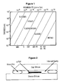
- Figure 1 shows the permeability rates of classes of materials, going from the very poor materials (silicones and epoxies) to the ultra-high vacuum materials (metals). These generic curves show that glasses typically have about 1000 times the permeation rate of metals. This means that: the gaseous permeation through a 1 square meter of sheet metal of a given thickness is equivalent to the permeation rate of about 1 square millimetre of sheet glass of the same thickness.
- a given surface of sealing metal can be about 30 times thinner than the same surface of sealing glass and provide the same sealing performance against gaseous permeation (permeation is a diffusion mechanism following the square root function of the diffusion equation). A given thickness of sealing metal will provide 30 times longer life than the same thickness of sealing glass. For this reason, metal sealing techniques are generally preferred over glass sealing techniques.
- the hermetic wafer-level packages should use the very low permeability characteristics of metal sealing materials for the wafer-level package to have a minimum gaseous permeation.
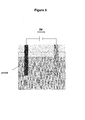
- FIG. 2 A first example of protective packaging is provided in Figure 2 taken from the following cited Prior Art references: USA patent 5,323,051 titled 'Semiconductor wafer level package'; USA patent 6,465,281 titled 'Method of manufacturing a semiconductor wafer level package'; and Gary Li, Ampere A. Tseng, 'Low stress packaging of a micromachined accelerometer', IEEE Transactions on electronics packaging manufacturing, Vol. 24, No. 1, January 2001 .
- This wafer-level packaging technique involves the use of a frit glass, such as: EG9251 manufactured by Ferro Corporation; CF-8 manufactured by Nippon Electric Glass Co. Ltd; VIOX Glass No. 24925 manufactured by VIOX Corporation; and VIOX Glass No. 24927 manufactured by VIOX Corporation.
- a frit glass such as: EG9251 manufactured by Ferro Corporation; CF-8 manufactured by Nippon Electric Glass Co. Ltd; VIOX Glass No. 24925 manufactured by VIOX Corporation; and VIOX Glass No. 24927 manufactured by VIOX Corporation.
- frit glasses are typically deposited on the "Lid wafer” using a slurry comprising a mixture of organic binder, solvent, and a frit glass containing filler, deposited through a silk screen. Following printing and heating to a high enough temperature to volatilize the organic and organic materials of this slurry, the "Lid wafer” and the “MEMS wafer” are contacted and pressed together and exposed to high enough temperature (less than 550°C, preferably about 300°C - 475°C) to exceed the softening point of the frit glass material and allow the thermo-compression bonding of the two wafers.
- high enough temperature less than 550°C, preferably about 300°C - 475°C
- the two main challenges associated with this wafer-level packaging are, first, the induced mechanical stress in the MEMS devices of the "MEMS wafer” due to the mismatch of the thermal expansion coefficients of the materials of this wafer-level package which are exposed to the high temperatures used to reach the softening point of the frit glass and, second, the slow gas permeation and micro-porosity of the obtained frit material which result in a slow contamination of the sealed micro-cavity with hydrogen and water vapor.
- a wafer-level packaging process capable of producing a hermetic seal at temperatures lower than about 300°C is preferred to minimize these induced mechanical stresses in the MEMS devices of the "MEMS wafer” and to ensure a stable gas composition in the sealed micro-cavity.
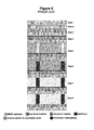
- FIG. 3 A second example of protective packaging is shown in Figure 3 taken from the following cited Prior Art reference: USA patent 5,952,572 titled 'Angular rate sensor and acceleration sensor' (Matsushita Electric Industrial Co., Ltd.).
- This technique requires the sodium atoms of a sodium-based silica glass (such as Corning Glass' PyrexTM 7740) to be diffused at a temperature of about 300-450°C and under a high electrical field created by a negative voltage of about 1000-2000V applied between the silicon substrate and the PyrexTM substrate as to allow sodium displacement of the silicon atoms of the substrate and the anodic bonding of the PyrexTM substrate to the silicon wafer.
- the anodic bonding temperature is not that lower than the one used for glass frit bonding and does not prevent the induced mechanical stresses in the MEMS devices of the "MEMS wafer".
- the sodium is an undesirable mobile ion inducing undesirable threshold voltage shifts of CMOS and high-voltage CMOS devices as well as dark-current issues in CCD devices.
- the seed layer of "MEMS wafers” is typically the last electrically conductive layer deposited on the "MEMS wafer” and may either be a doped silicon layer or a metal layer.
- the nickel under-layer structure of a wafer-level package can be made using electrolytic plating technologies to create the nickel under-layer structures of sealing rings on the "MEMS wafer” (around each individual die) and a symmetrical sealing rings on the "Lid wafer". These two symmetrical nickel-based sealing rings allow the soldering of the "MEMS wafer” to the "Lid wafer” using a whisker-free solder (following proper alignment and physical contact of the symmetrical structures of the two wafers).
- the main advantages of electrolytic plating of nickel under-layer structures are: accurate, low-cost, easy, and quick process; low-temperature process, compatible with the thermal budgets required to produce MEMS structures over CMOS and HV-CMOS devices; high aspect ratio under-layer structures when electroplated through very thick (10 ⁇ m to 1mm) and narrow (one micron to a few microns) openings created using high-sensitivity photo-sensitive polymer exposed and developed with standard UV lithography and used as mold (a technique also called electro-forming).
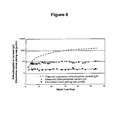
- Figure 4 is taken from USA patent 6,411,754 to Coming Incorporated and shows a MEMS-based photonics mirror obtained from electrolytic plating of nickel over a 0.5 ⁇ m thick evaporated copper seed layer and into a mold as to form an integral electrode structure.
- This 6 ⁇ m thick nickel layer is plated from a nickel sulfate solution at about 45°C.
- FIG 5 is a sketch of a typical electrolytic plating set-up, called an electrolytic cell, where the MEMS wafer (or Lid wafer) is immersed in an electroplating solution to plate the electrolytic nickel under-structures.
- the anode provides the source of nickel and the chemical solution provides the cathode.
- the Ni 2+ ions are neutralized by the electrons at the surface of the wafer.
- This MEMS wafer (or Lid wafer) is connected to a negative potential relative to a positive electrode typically consisted of the electroplating nickel metal anode that is also immersed in the plating solution. If sufficient bias is imposed between the two electrodes, electrons will flow through the power supply from the anode (the nickel electrode) to the cathode (the surface of exposed conductor of the wafer in contact with the plating solution). Near the cathode, a reduction reaction (gain of electron) occurs, resulting in the plating of a nickel under-structure onto the exposed surface: Ni 2+ ⁇ 2 e - + Ni
- This reduction mechanism requires an electrical current to be continuously supplied to the growing nickel under-structure so as to neutralize, at the surface, the incoming Ni 2+ ions supplied by the plating solution.
- the current is conducted by the flow of positive ions and an oxidation reaction (loss of electrons) occurs near the nickel anode: Ni ⁇ 2 e - + Ni 2+ where the nickel atoms of the anode are dissolved into the plating solution.
- This reaction supplied the two electrons flowing into the power supply and the nickel ion migrating into the solution toward the wafer cathode.
- the supplied current controls the neutralization rate and then the flow of migrating nickel ions, i.e. the electrolytic plating rate.
- This hydrogen reduction reaction competes with the nickel deposition and should be avoided. An excess amount of hydrogen also deteriorates the quality of plated nickel.
- Figure 6 shows an example of electroplating process resulting in the selective formation of nickel under-structures through a polymer pattern on a flat surface wafer.
- the process consists of the following steps:
- This removal is relatively simple if a selective etch can remove this "continuous and unbroken seed layer" from the areas previously coated with the polymer without attacking the plated nickel under-structures.
- the complete removal of this "unbroken and continuous seed layer" from the areas previously coated with the polymer is not obvious on the non-flat surface of an advanced MEMS wafer already presenting high aspect ratio structures and topography.
- Figure 7 shows an example of an electroplating process over the non-flat surface af an advanced MEMS wafer presenting high aspect-ratio structures and topography. This process consists of the following steps:
- the sacrificial layer is patterned such as to create openings or anchors of the nickel under-structures to the substrate (or to any other non-sacrificial layer) and as to later allow the mechanical release of non-anchored structures.
- Advanced MEMS use thicker and narrower suspended structures and multi-level structures with smaller spacings as to enhance electrostatic sensing and actuation. This means that the "continuous and unbroken seed layer" is to be deposited as thin as possible (as to minimize the undercut resulting from its local removal later in the process) on increasingly complex high aspect ratio structures.
- EP 0 962 275 discloses a method of soldering using seed layers, structural underlayers, anti-oxidant layers and a layer of solder.
- the present invention relates to a new technique for producing hermetically sealed micro-cavities between the "Lid wafer” and the "MEMS wafer” so as to control the micro-environment around the MEMS devices.
- This new technique is compatible with the low-temperature requirements of all known wafer-level packages for MEMS devices and the recent lead-free requirements of the electronics industry.
- This new technique also prevents the whisker problem typically associated with lead-free tin-based solders.
- this new technique is CMOS and CCD compatible so it allows advanced MEMS to be fabricated over integrated circuits in a single manufacturing line, without the contamination problems associated with gold or with the sodium atoms typically used in alternate wafer-level packaging techniques.
- the new wafer-level package requires the bonding of the "Lid wafer” to the "MEMS wafer” to form a sealed micro-cavity over each individual MEMS devices of the "MEMS wafer". Since the vacuum level or pre-set pressure in each micro-cavity is to be maintained in the field for about 10 years, it is necessary to use metal-based sealing materials capable of preventing gas permeation from the external world to the inside of these micro-cavities.
- a method of making a wafer-level package for a plurality of MEMS devices, wherein a sealed and hermetic micro-cavity is formed over each MEMS device comprising: preparing a MEMS wafer with a first bonding structure; preparing a lid wafer with a second bonding structure; and bonding said lid wafer to said MEMS wafer through said first and second bonding structures to create said wafer level package, and wherein said lid wafer and said MEMS wafer are substantially free of at least one component selected from the group consisting of alkali metals and chlorine; wherein said first bonding structure comprises a first seed layer on a MEMS device, a first structural underlayer over said first seed layer, and a first anti-oxidation layer over said first structural underlayer; wherein said second bonding structure comprises a second seed layer, a second structural underlayer over said second seed layer, a second anti-oxidation layer over said second structural underlayer, and a layer of lead-free solder capable of bonding to
- Electroless plating is a known technique allowing the plating of metals and/or alloys without the need for the continuous seed layer to be removed after plating.
- the simplest form of electroless plating is the so-called metal displacement oxidation/reduction reaction.
- An example of such metal displacement reaction is readily observed when a zinc metal is immersed in a copper sulfate solution: The zinc atoms (less noble) dissolve into the solution and are spontaneously replaced by copper atoms from the solution.
- the plating of nickel under-structures by metal displacement is limited to deposits of only about 0.2 ⁇ m thickness.
- the plating of nickel under-structures by metal displacement is limited to deposits of only about 0.2 ⁇ m thickness.
- the plating of nickel under-structures by metal displacement is limited to deposits of only about 0.2 ⁇ m thickness.
- This autocatalytic nickel plating process is the result of a series of electrochemical reactions involving the sustained catalyzed reduction of the Ni +2 cations by the H 2 PO 2 - anions produced by the mixed aqueous solution of the two salts, namely
- Ni +2 The production of nickel cations, Ni +2 , from the nickel sulfite: NiSO 4 ⁇ Ni +2 + SO 4 -2
- hypophosphite anions H 2 PO 2 -
- hypophosphite anions H 2 PO 2 -
- the heterogeneous reactions outlined above are autocatalytic on these interfaces capable of ion and electron exchanges with the plating solution. Hence, electroless plating of nickel under-structures occurs only on these specific surfaces.
- the catalyzed reduction of the Ni +2 cations by the H 2 PO 2 - anions at these interfaces begins spontaneously on certain metals and on almost all metals of Group VIII of the periodic table (Fe, Co, Ni, Rh, Pd, Pt) which are well known as hydrogenation-dehydrogenation catalysts.
- Metals that are more electropositive than nickel, such as aluminium, will first displace nickel from a solution of its Ni +2 ions, thus forming the nickel catalytic surface: i.e. when exposed aluminum surfaces are electroless plated with nickel under-structures, the initial phase of the deposition process is a displacement reaction similar to the upper-described copper-zinc displacement reaction.
- the sustained reduction of the Ni +2 cations by the H 2 PO 2 - anions at the exposed interfaces takes place in most cases at temperatures between 70°C and 93°C as well as pH conditions between 4.2 to 6.5.
- the electrolyte must be balanced regarding the content of nickel sulfite (consumed), of sodium hypophosphite (transformed into sodium orthophosphite, NaH 2 PO 3 ) and of OH - ions (the consumption of nickel sulfite induces the formation of sulphuric acid, H 2 SO 4 , accumulating in the bath thus decreasing the pH, thus lowering the formation of the required OH - ions and slowing-down the plating rate).
- an alkaline medium such as ammonium hydroxide, NH 4 OH
- An electroless nickel bath having initially 7 g/l of nickel sulfite produces approximately 28 g/l of sodium orthophosphite as by-product of the electroless plating reaction.
- NiSO 4 ⁇ 6H 2 O nickel sulfate
- electroless nickel plating solutions have a limited life measured by the number of "Metal Turn-Overs", MTOs; i.e. the number of complete bath replenishments made using nickel sulfate salts to recharge the bath to the 7 g/l nickel concentration.
- Electroless nickel baths made using nickel sulfate and sodium hypophosphate salts typically have a very short bath life of about 5-8 MTOs.
- This autocatalytic electroless plating of nickel under-structures involving the use of hypophosphite anions, H 2 PO 2 - , produced by a sodium hypophosphite, 2NaH 2 PO 2 , in aqueous solution and capable of sustained reduction of the Ni +2 cations prevents the use of the continuous seed layer but does not solve the problem associated with sodium, this undesirable mobile ion inducing threshold voltage shifts of CMOS and high-voltage CMOS devices as well as dark-current issues in CCD devices.
- Ni +2 The production of nickel cations, Ni +2 , from the nickel sulfite: NiSO 4 ⁇ Ni +2 + SO 4 -2
- hypophosphite anions H 2 PO 2 -
- Metal nickel is again electroless plated at interfaces with the plating solution which are capable of charge and ion exchanges: 2H 2 PO 2 - (at interface) ⁇ 2HPO 2 - (from interface) + H 2 ⁇ (from interface) 2H 2 O ⁇ 2H + (from interface) + 2OH - (from interface) 2HPO 2 - (at interface) + 2OH - (at interface) ⁇ 2H 2 PO 3 - (from interface) + e Ni +2 (at interface) + 2e (at interface) ⁇ Ni 0 (on interface) 2H + (at interface) + SO 4 -2 (at interface) ⁇ H 2 SO 4 (from interface) Ni +2 (at interface) + 2H 2 PO 3 - (at interface) ⁇ Ni(H 2 PO 3 ) 2 (from interface) resulting in the following autocatalytic nickel plating reaction: NiSO 4 + Ni(H 2 PO 2 ) 2 + 2H 2 O ⁇ Ni 0 + H 2 SO 4 + Ni(H 2 PO 3 ) 2 + H
- the heterogeneous reactions outlined above are autocatalytic on these interfaces capable of ion and electron exchanges with the plating solution and metals that are more electropositive than nickel, such as aluminum, will first displace nickel from a solution of its Ni +2 ions, thus forming the nickel catalytic surface: i.e. when exposed aluminum surfaces are plated with electroless nickel under-structures, the initial phase of the deposition process is the a displacement reaction similar to the upper-described copper-zinc displacement reaction.
- This autocatalytic electroless plating of nickel under-structures involving the use of hypophosphite anions, H 2 PO 2 - , produced by a nickel hypophosphite, Ni(H 2 PO 2 ) 2 in aqueous solution to reduce the Ni +2 cations and deposit a metal nickel under-structure without the use of the continuous seed layer solves the problem associated with sodium, this undesirable mobile ion inducing threshold voltage shifts of CMOS and high-voltage CMOS devices as well as dark-current issues in CCD devices.
- Ni(H 2 PO 2 ) 2 the nickel hypophosphite
- the nickel orthophosphite, Ni(H 2 PO 3 ) 2 results in the transformation of nickel sulfite into sulfuric acid, H 2 SO 4 , and sulfates accumulating in the bath as contaminants decreasing the pH, thus lowering the formation of the required OH - ions and slowing-down the plating rate.
- nickel sulfite-based electroless nickel processes result in sulfuric acid and other undesirable sulfate by-products which cause unstable plating processes and short MTOs. It is then desirable to get rid of this nickel sulfate salt.
- a replacement nickel salt, nickel chloride could not be used to plate nickel under-structures over exposed aluminium surfaces and/or aluminium interconnects because the chloride anion will act deleteriously on these exposed aluminium surfaces and/or aluminium interconnects.
- nickel hypophosphite Ni(H 2 PO 2 ) 2
- Ni(H 2 PO 2 ) 2 nickel hypophosphite
- the use of nickel hypophosphite as a dual source increases the stability and reduces the change-out frequency of the electroless nickel plating bath as well as increases the number of MTOs since there are no sulfates involved and much less undesirable by-products formation from the following chemical reactions:
- Ni +2 The production of nickel cations, Ni +2 , from a nickel hypophosphite molecule: Ni(H 2 PO 2 ) 2 ⁇ Ni +2 + 2H 2 PO 2 -
- hypophosphite anions H 2 PO 2 -
- Metal nickel is again electroless plated at interfaces with the plating solution which are capable of charge and ion exchanges: 2H 2 PO 2 - (at interface) ⁇ 2HPO 2 - (from interface) + H 2 ⁇ (from interface) 2H 2 O ⁇ 2H + (from interface) + 2OH - (from interface) 2HPO 2 - (at interface) + 2OH - (at interface) ⁇ 2 H 2 PO 3 - (from interface) + 2e Ni +2 (at interface) + 2e (at interface) Ni 0 (on interface) 2H + (at interface) + 2H 2 PO 2 - (at interface) ⁇ 2H 3 PO 2 (from interface) Ni +2 (at interface) + 2H 2 PO 3 - (at interface) ⁇ Ni(H 2 PO 3 ) 2 (from interface) resulting in the following autocatalytic nickel plating reaction: Ni(H 2 PO 2 ) 2 + Ni(H 2 PO 2 ) 2 + 2H 2 O ⁇ Ni 0 + 2H 3 PO 2 + Ni(
- heterogeneous reactions outlined above are autocatalytic on these interfaces capable of ion and electron exchanges with the plating solution and metals that are more electropositive than nickel, such as aluminium, will first displace nickel from a solution of its Ni +2 ions, thus forming the nickel catalytic surface.
- the oxidation of nickel hypophosphite, Ni(H 2 PO 2 ) 2 results in the formation of nickel orthophosphite, Ni(H 2 PO 3 ) 2 , this white slurry-like by-product precipitating into the plating solution.
- the consumption of nickel from the nickel hypophosphite also produces hypophosphite acid, H 3 PO 2 , which accumulates in the bath as a contaminant decreasing the pH, thus lowering the formation of the required OH - ions and slowing-down the plating rate.
- the progressive adding of compensating chemicals to maintain the pH and to stabilize the plating rate changes the mechanical properties of the electroless plated nickel under-structures and reduces the bath life, i.e. the number of Metal Turn-Overs, MTOs.
- nickel hypophosphate salts as source of Ni 0 metal nickel as well as source of reducing H 2 PO 2 - anion increases the stability and reduces the change-out frequency of the electroless nickel plating bath as well as increases the number of MTOs because no sulfates are involved and much less undesirable by-products are formed as the result of the electroless plating.
- compensating alkali chemicals such as ammonium hydroxide, NH 4 OH, are progressively added.
- Figure 8 which is a re-sketch taken from the above-cited J.Cl. Puippe reference, shows the improvement made by the EDEN bath life extension process on the life of electroless nickel bath: From about 200 g/l of cumulated orthophosphite, or about 7 MTOs (at 28 g/l of orthophosphite per MTO) without EDEN to an extended equivalent concentration of orthophosphite (removed by electrodialysis) of more than 2.5 kg/l, or more than 100 MTOs using EDEN life extension electrodialysis to remove the orthophosphite.
- This spectacular reduction of plating chemicals by more than 90% is also associated to a more stable electroless plating process, as evidenced by the very stable plating rate over these 100 MTOs.
- Figure 9 shows that this particular EDEN life extension process cannot be used for the stable production of electroless nickel under-structures involved in wafer-level packages of advanced MEMS involving CMOS, high-voltage CMOS and/or CCD devices because its operation is based on the use of sodium hydroxide, NaOH: A generator of unfriendly sodium mobile ions.
- the "URIity" electroless nickel process uses nickel hypophosphite, Ni(H 2 PO 2 ) 2 , as source of metal and as reducing agent, ammonium hydroxide, NH 4 OH, as pH adjuster and trace amount of hydroxy-2 ethylene diamine triacetic acid (HEEDTA), C 10 H 18 O 7 N 2 , a safe high-melting-point organic acid.
- This electroless nickel plating solution DOES NOT use any sodium hypophosphite, NaH 2 PO 2 , or nickel sulfate, NiSO 4 , as reducer and source of metal and then eliminates two of the three ions by-products (sodium and sulfate).
- the third ion, orthophosphite is removed using a simple chemical reaction with calcium hydroxide, CaOH, and the treated solution is returned to the process cell to adjust the pH.
- orthophosphite ions and trace contaminants Na, Ca, Pb, Mo
- all other useful ions must be balanced using a reactor, an ion exchange ceramic filter, a centrifuge and four primary materials continuously added to the process that treats a small portion of the plating solution: Nickel hypophosphite, ammonium hydroxide, calcium hydroxide and carbon dioxide which treats the calcium hydroxide and maintains the calcium level to less than about 30 ppm.
- the purified solution is centrifuged removing the calcium orthophosphite as a solid which is discharged from the centrifuge as a slurry.
- This non-hazardous calcium orthophosphite slurry also contains trace amounts of nickel.
- the process is controlled tightly via the monitoring of the process temperature, of the process pH at about 4.8 (via an automatic sampling), of the nickel and hypophosphite concentrations (using an automatic titration every 15 minutes), of the water level, of the process pressure and of the hydrogen evolution of the exhaust flow (for operator safety).
- the calcium-hydroxide based "UNIity" life extension process CAN be used for the stable production of electroless nickel under-structures involved in wafer-level packages of advanced MEMS involving CMOS, high-voltage CMOS and/or CCD devices.
- Electroless nickel (and other electroless metals) is prone to oxidation upon exposure to air and forms a thin layer of a very stable oxide which prevents proper soldering to the solder of the "Lid wafer". Extremely corrosive fluxes, which would alleviate this problem, are unsuitable for wafer-level packages situations. This implies that electroless nickel cannot be used alone without a thin anti-oxidation layer as its oxide prevents proper solder wetting of the nickel surface.
- a noble metal layer capable of metal displacement of the electroless nickel (or other electroless plated materials that are covered by the present patent application) would be efficient as anti-oxidation layer.
- the metal displacement plating also called immersion plating
- This autocatalytic noble metal displacement reaction result in the displacement of the exposed surface of nickel metal atoms by the noble metal cations present in the electrolyte solution. Again, this immersion plating reaction is initially observed as a mosaic of anodic nickel and cathodic noble metal sites until almost the entire substrate of nickel is covered with the noble metal. At this point, the oxidation of the nickel anode virtually stops and the noble metal plating process ceases.
- Figure 10 shows a prior art process using immersion and/or electroless gold as an anti-oxidation protective layer. This process consists of the following steps:
- the immersion and/or electroless plating of the noble metal layer on the top of the electroless nickel prevents the oxidation of the top surface of nickel and enhances the adhesion of the solder to this top nickel surface by allowing proper wetting and soldering to the noble metal layer.
- wafer-level packages require to be hermetic, immersion and/or electroless palladium should be avoided as the anti-oxidation layer over electroless nickel in hermetically sealed wafer-level packages because its hydrogen permeation and hydrogen-induced embrittlement properties. It is necessary to find another noble metal than gold or palladium.
- this reaction stops when the platinum atoms cannot reach the underlying nickel surface anymore.
- platinum could be further reduced by one chemical of the solution itself as to achieve a sustained electroless platinum plating.
- Various chemical solutions are capable of this sustained electroless platinum, including alkali-based solutions, hydrazine-based solutions, chlorine-based solutions and others.
- One possible reducing chemical capable of reducing the platinum cations, Pt +2 , of the platinum sulfite solution is sodium hypophosphite obtained from the dissolution of sodium hypophosphate salt: Sodium hypophosphate (NaH 2 PO 2 ⁇ H 2 O).
- This platinum sulfite and sodium hypophosphite solution could be used as a supplement to the limited platinum displacement reaction since it is capable of a sustained electroless plating of the anti-oxidation layer resulting from the replenishing effect of the dissolved platinum sulfate tetrahydrate salt in the solution, a continuous source of platinum replacing the platinum that has been plated.
- This autocatalytic platinum plating process is the result of a series of electrochemical reactions involving the sustained catalyzed reduction of the Pt +2 cations by the H 2 PO 2 - anions produced by the mixed aqueous solution of the two salts.
- Platinum cations, Pt +2 can be produced from platinum sulfite by the following process, which results in the electroless plating of nickel metal containing a small amount of phosphorus at interfaces with the plating solution which are capable of charge and ion exchanges: 4NaH 2 PO 2 ⁇ 4Na + + 4H 2 PO 2 - 4H 2 PO 2 (at interface) ⁇ 4HPO 2 - (at interface) + 2H 2 ⁇ (from interface) 4H 2 O ⁇ 2H + (from interface) + 4OH - (from interface) 4HPO 2 - (at interface) + 4OH - (at interface) ⁇ 4H 2 PO 3 - (from interface) + 4e - Pt(SO 4 ) 2 + 2e - (at interface) ⁇ Pt +2 (at interface) + 2(SO 4 ) -2 (at interface) Pt +2 (at interface) + 2e - (at interface) ⁇ Pt 0 (on interface) 2H + (at interface) + 2SO 4
- heterogeneous reactions outlined above are autocatalytic on these interfaces capable of ion and electron exchanges with the plating solution. Hence, electroless plating of platinum occurs only on these specific surfaces.
- the sustained reduction of the Pt +2 cations by the H 2 PO 2 - anions requires the electrolyte to be balanced regarding the content of platinum sulfite (consumed), of sodium hypophosphite (transformed into sodium orthophosphite, NaH 2 PO 3 ) and of OH - ions (the consumption of platinum sulfite induces the formation of sulphuric acid, H 2 SO 4 , accumulating in the bath thus decreasing the pH, thus lowering the formation of the required OH - ions and slowing-down the plating rate).
- an alkaline medium such as ammonium hydroxide, NH 4 OH, allows the pH stabilization to its nominal value.
- sodium-based chemicals such as sodium hydroxide as pH adjuster, disodium hydrogen phosphate salt as reducing agent, sodium nitrite as stabilizer, or any other sodium-based chemicals used to enhance and/or stabilize the electroless reaction do generate undesirable sodium mobile cations, Na + , and prevent the use of these sodium-based electroless plating solutions to plate electroless platinum over electroless nickel under-structures for wafer-level packages of advanced MEMS involving CMOS, high-voltage CMOS and/or CCD devices.
- sodium hydroxide as pH adjuster
- disodium hydrogen phosphate salt as reducing agent
- sodium nitrite sodium nitrite
- any other sodium-based chemicals used to enhance and/or stabilize the electroless reaction do generate undesirable sodium mobile cations, Na + , and prevent the use of these sodium-based electroless plating solutions to plate electroless platinum over electroless nickel under-structures for wafer-level packages of advanced MEMS involving CMOS, high-voltage CMOS and/or CCD devices.
- platinum can effectively be electroless plated using an acidic solution made of a water-soluble platinum salt such as diamminebis(nitro-N,N) platinum (DNP), Pt(NH 3 ) 2 (NO 2 ) 2 , as source of platinum, hydrazine hydrate, N 2 H 4 ⁇ H 2 O, as reducing agent added just before plating as well as acetic acid, CH 3 COOH, or nitric acid, HNO 3 , as pH adjuster.
- a water-soluble platinum salt such as diamminebis(nitro-N,N) platinum (DNP), Pt(NH 3 ) 2 (NO 2 ) 2 , as source of platinum, hydrazine hydrate, N 2 H 4 ⁇ H 2 O, as reducing agent added just before plating as well as acetic acid, CH 3 COOH, or nitric acid, HNO 3 , as pH adjuster.
- DNP diamminebis(nitro-N,N) platinum
- This acidic electroless plating solution over the other alkaline electroless solutions is the elimination of the sodium mobile cations, Na + , which allow the plating of electroless platinum over electroless nickel under-structures for wafer-level packages of advanced MEMS involving CMOS, high-voltage CMOS and/or CCD devices.
- hydrazine-based immersion and/or electroless platinum should be avoided as the anti-oxidation layer over electroless nickel.
- a cost-effective and production worthy electroless plating process requires the sequential plating of the underlying nickel (or other under-layer material) and of the anti-oxidation layer of noble metal over the seed layer is an aluminium alloy which is very susceptible to corrosion when exposed to trace levels of chlorine.
- the chlorine-based immersion and/or electroless platinum plating solutions are then to be avoided to prevent corrosion and reliability issues in the field of advanced MEMS involving CMOS, high-voltage CMOS and/or CCD devices and thus aluminium-based interconnects.
- the USA Patent 5,384,284 describes an electroless platinum solution of platinum sulfate, Pt(SO 4 ) 2 , and ethylenediaminetetraacetic acid (EDTA, also called ethylenedinitrilotetracetatic acid), C 10 H 16 N 2 O 8 .
- This solution is interesting because the following material safety data sheets (MSDS) show that EDTA is much more safe to use than hydrazine: EDTA MSDS from University of Oxford; EDTA MSDS from RPI; EDTA MSDS from J.T. Baker.
- the immersion platinum process using an alkali-free, hydrazine-free and chlorine-free plating solution is: Compatible with CMOS, high-voltage CMOS and CCD; Safer to use than hydrazine-based solutions; Aluminium corrosion-proof because it is free from chlorine and probably reliable for advanced MEMS devices incorporating aluminium-based interconnects; and Capable of producing solderable nickel surfaces because over-coated with a thin layer of non-oxidable platinum;
- the electroless platinum process using an alkali-free (sodium-free, potassium-free, lithium-free), hydrazine-free and chlorine-free platinum sulfate and EDTA based plating solution also has the same good characteristics and is also capable of thicker platinum deposits over electroless nickel under-layer material.
- platinum is a precious noble metal, it would be preferred (if possible) to use one of the other two possible noble metals: Rhodium or ruthenium. In that case, it is again required to use an alkali-free, an hydrazine-free and a chlorine-free plating solution of this other noble metal.
- this reaction stops when the rhodium atoms cannot reach the underlying nickel surface anymore.
- rhodium could be further reduced by one chemical of the solution itself as to achieve a sustained electroless rhodium plating.
- Rhodium trichloridtrihydral RhCl 3 ⁇ 3H 2 O
- RhCl 3 ⁇ 3H 2 O is used as source of rhodium, thus producing undesirable chlorine ions
- Hydrazine monohydrate, N 2 H 4 ⁇ H2O is used as reducing agent, thus causing an unsafe plating bath for the operators
- Disodium hydrogen phosphate, Na 2 HPO 4 ⁇ 12H 2 O is also used as reducing agent, thus a source of undesirable sodium cations
- Sodium nitrite, NaNO 2 is used as stabilizer, thus another source of undesirable sodium cations.
- a DMAB-based plating solution which is undesirable because: even if the rhodium sulfate, Rh(SO 4 ) 2 ⁇ 4H 2 O, used as the rhodium-containing soluble compound is free of alkali and chlorine ions; even if the ammonium hydroxide, NH 4 OH, used as buffer to control the pH is free of undesirable sodium cations; dimethylamine borane (DMAB), (CH 3 ) 2 NHBH 3 , used as reducing agent is effectively free of alkali and chlorine ions but is as toxic as hydrazine, N 2 H 4 , as shown by the following Material Safety Data Sheets (MSDS): DMAB MSDS from Callery Chemicals; DMAB MSDS from Shipley Company; DMAB MSDS from University of Oxford.
- MSDS Material Safety Data Sheets
- An EDTA-based plating solution which is desirable because: the rhodium sulfate, Rh(SO 4 ) 2 ⁇ 4H 2 O, used as the rhodium-containing soluble compound is free of alkali and chlorine ions; the ammonium hydroxide, NH 4 OH, used as buffer to control the pH is free of undesirable sodium cations; the ethylenediaminetetraacetic acid (EDTA, also called ethylenedinitrilotetracetatic acid), C 10 H 16 N 2 O 8 , used as the complexing agent is free of alkali and chlorine ions and is safer than hydrazine, N 2 H 4 , and safer than dimethylamine borane (DMAB), (CH 3 ) 2 NHBH 3 , as shown by the following material safety data sheets (MSDS): EDTA MSDS from University of Oxford; EDTA MSDS from RPI; EDTA MSDS from J.T. Baker;
- MSDS material safety data sheets
- the immersion rhodium process using an alkali-free, hydrazine-free and chlorine-free plating solution is: Compatible with CMOS, high-voltage CMOS and CCD; Safer to use than hydrazine-based solutions; Aluminium corrosion-proof because it is free from chlorine and probably reliable for advanced MEMS devices incorporating aluminium-based interconnects; Capable of producing solderable nickel surfaces because over-coated with a thin layer of non-oxidable rhodium.
- the electroless rhodium process using an alkali-free (sodium-free, potassium-free, lithium-free), hydrazine-free and chlorine-free rhodium sulfate and EDTA based plating solution also has the same good characteristics and is also capable of thicker rhodium deposits over electroless nickel under-layer material (or other under-layer material).
- this reaction stops when the ruthenium atoms cannot reach the underlying nickel surface anymore.
- ruthenium could be further reduced by one chemical of the solution itself as to achieve a sustained electroless ruthenium plating.
- D.S. Cameron describes in his USA patent 4,414,071 an electroless ruthenium plating solution made from ruthenium trichloride, RuCl 3 , and hydrochloric acid, HCl, as to achieve ruthenium electroless plating at a pH of 1.8 and a temperature of 80°C.
- RuCl 3 ruthenium trichloride
- HCl hydrochloric acid
- the required cost-effective and production worthy electroless plating process should sequentially plate the underlying nickel and the ruthenium layer over a seed layer is an aluminium alloy which is very susceptible to corrosion when exposed to trace levels of chlorine.
- This chlorine-based electroless ruthenium plating solutions is then to be avoided as to prevent corrosion and reliability issues in the field of advanced MEMS involving CMOS, high-voltage CMOS and/or CCD devices and thus aluminium-based interconnects.
- R. Redline describes in his USA patent 6,120,639 electroless ruthenium plating solutions made of ruthenium sulfate, RuSO 4 , as source of ruthenium and of one of the following reducing agent: Sodium hypophosphite, NaH 2 PO 2 , which is undesirable due to the presence of mobile sodium ions and thus incompatible with CMOS, high-voltage CMOS and CCD; Potassium hypophosphite, KH 2 PO 2 , which is also undesirable due to the presence of mobile sodium ions and thus incompatible with CMOS, high-voltage CMOS and CCD; Sodium borohydride, BNaH 4 , which is also undesirable due to the presence of mobile sodium ions and thus incompatible with CMOS, high-voltage CMOS and CCD; Dimethylamine borane (DMAB), (CH 3 ) 2 NHBH 3 , which is also undesirable because as toxic as hydrazine, N 2 H 4 , as shown by the following Material Safety Data Sheets
- This ruthenium sulfate-based electroless ruthenium plating solutions is then to be avoided as to prevent mobile ions problems in advanced MEMS involving CMOS, high-voltage CMOS and/or CCD devices and thus aluminium-based interconnects. Moreover, it is to be avoided because unsafe for the health and safety of the operators of the electroless ruthenium plating bath.
- the anti-oxidation layer could be electroless platinum, either limited by the displacement of the underlying metal, Me, using an alkali-free (sodium-free, potassium-free and lithium-free), chlorine-free solution: 2Me 0 + nPt 2+ ⁇ 2Me n+ + nPt 0 or by electroless plating of a thicker layer using an alkali-free (sodium-free, potassium-free and lithium-free), chlorine-free, hydrazine-free, dimethylamine borane-free (DMAB-free) electroless plating solution; could be electroless rhodium, either limited by the displacement of the underlying metal, Me, using an alkali-free (sodium-free, potassium-free and lithium-free), chlorine-free solution: 2Me 0 + nRh 2+ ⁇ 2Me n+ + nRh 0 or by electroless plating of a thicker layer using an alkali-free (sodium-free, potassium
- the seed layer of "Lid wafer” is typically an electrically conductive layer deposited on the “Lid wafer” and may either be a doped silicon layer or a metal layer.
- the structural under-layer in accordance with the invention is again deposited using electroless plating technologies.
- Nickel chloride-based baths should be avoided because the chloride anion will act deleteriously on these exposed aluminium surfaces and/or aluminium interconnects. Hydrazine-based baths should be avoided to prevent health and safety problems. Alkali-based (sodium-based, potassium-based or lithium-based) baths should be avoided to avoid the undesirable mobile ions problems in advanced MEMS involving CMOS, high-voltage CMOS and/or CCD devices.
- the anti-oxidation layer of the lid wafer can be electroless platinum, electroless rhodium or electroless ruthenium, either limited by the displacement of the underlying metal.
- DMAB-free dimethylamine borane-free
- the “Lid wafers” are also to be electroless plated with the solder itself which will adhere to the underlying anti-oxidation layer of the "Lid wafer", even above its liquidus temperature, as which will wet the anti-oxidation layer of the "MEMS wafer” upon contact and solder the two wafers when the temperature will be dropped below the liquidus temperature, thus forming the sealed micro-cavities of the wafer-level package.
- solder used in a metal-sealed wafer-level package is provided in Figure 12 taken from the following cited Prior Art reference: USA patent 6,563,106 titled 'Micro-electro-mechanical-system (MEMS) mirror device and methods for fabricating the same'.
- MEMS micro-electro-mechanical-system
- a tin-lead solder is used to ensure the hermetic bonding of the "Lid wafer” to the "MEMS wafer” as to form the micro-cavities of the wafer-level package of a MEMS mirror used in photonics applications.
- Pb-Sn solders allows the bonding temperature to be reduced to less than 300°C.
- the Pb-Sn phase diagram of Figure 13 shows that the very popular 74wt%Sn-26wt%Pd solder has an eutectic formation at a temperature of only 183°C. This means that this very popular alloy can bond the "MEMS wafer” and the "Lid wafer” at such a low temperature.
- Cookson has lead-free solutions for its customers.
- Coretec has six lead-free surface finish options (HASL, immersion Sn, immersion Au, immersion Ag and two OSP's).
- Motorola SPS has qualified some components with Ni/Pd lead frames and is investigating technology to provide both lead-free & halogen-free leaded & BGA components to enable its customers to meet the requirements of the WEEE Directive.
- Shipley Co. LLC Developing lead-free electronic materials through the Shipley Ronal Division, and are currently offering/developing lead-free finishes for components/connectors (Sn, SnCu, SnBi, SnAg) and PWB final finish applications (ENIG, electroless Pd, immersion silver, immersion tin, OSP).
- Teledyne Halco has a lead-free HASL process that is compatible with PCB manufacturing and assembly standards since 2001.
- Texas Instruments introduced a nickel/palladium (Ni/Pd) finish, a lead-free alternative, to the IC market in 1989, and there are currently, more than 30 billion TI lead-free Ni/Pd components in the field.
- Visteon is evaluating Sn3.5Ag, Sn4Ag0.5Cu and quaternary lead-free solders.
- Lead solders restrictions will be in effect on July 1 st 2006; In Germany , via the http://www.zvei.org/bleiok ; In Denmark , the Danish Environment Agency has signed a statutory order on prohibition of import, marketing and manufacture of lead and products containing lead. This Order affects the import, marketing and manufacture of lead and certain products containing lead according to the listing in the full text of the document. In this case lead has been defined as products in which lead represents more than 100 ppm (0.1mg/kg) of their homogeneous components.
- lead-based solders will have to be replaced by other lead-free low-temperature solders capable of similar low-temperature waver bonding as to avoid future environmental issues.
- the techniques involving lead-containing solders and materials are to be avoided for the production of wafer-level packages for advanced MEMS devices.
- the "Lead-Free Assembly & Rework Project” has clearly shown that, unlike lead-based solders, lead-free tin-based solders are prone to the formation of whiskers at room temperature and over time.
- Figure 14 shows the kind of whiskers which can grow at room temperature over time in lead-free tin-based solders, as recently disclosed in a few recent reports covering the reliability of lead-free tin-based solders: I. Boguslavsky, “Whiskers: Truth and Whiskers: Truth and Mystery”, IPC/NEMI Symposium on Lead-Free Electronics, September 19, 2002, Montreal, Canada ; Chen Xu, Yun Zhang*, C. Fan and J. Abys, "Understanding Whisker Phenomenon: Driving Force for Whisker Formation”, Cookson Electronics, 2002 ; “ Tin Whisker Info Brief", ON Semiconductor Application Note, TND311/D, May, 2003, Rev. 0 .
- whiskers can be prevented if, either: The lead-free tin-based solders are fabricated as to achieve a tensile mechanical stress; A nickel layer is positioned under and over the lead-free solders prone to whiskers as to prevent their interaction with the underlying and overlying metals.
- Gallium has a low melting point of only 29.8°C and will be treated in this invention as a "cold" solder. There are no prior art documents describing electroless gallium plating solutions.
- Indium has also a relatively low melting point of only 156.8°C and will be treated in this invention as a "warm” solder.
- the following Prior Art references describe the various electroless indium plating solutions: USA Patent 4,935,312 titled “Film carrier having tin and indium plated layers”; USA Patent 4,959,278 titled “Tin whisker-free tin or tin alloy plated article and coating technique thereof'; USA Patent 5,160,373 titled “Electroless plating bath”; USA Patent 6,221,530 titled “Mercury-free zinc anode for electromechanical cell and method for making same”.
- Shimauchi describes in his USA patent 4,959,278 three electroless indium plating solutions: a sodium-based indium electroless plating bath containing a sodium borohydride, NaBH 3 , as a reducing agent, which is not CMOS compatible; a chlorine-based indium electroless plating bath containing a hydrochloric acid, HCl, thiourea, (NH 2 ) 2 CS, and indium chloride, InCl 3 ⁇ 2H 2 O.
- This chlorinated solution is undesirable because the aluminium alloys composing the advanced MEMS devices are very susceptible to corrosion when exposed to trace levels of chlorine and then, chlorine-free plating chemistries are desirable.
- a CMOS compatible, chlorine-free and operator safe electroless indium plating bath containing: a chlorine-free and alkali-free source of indium: Indium sulfate, In 2 (SO 4 ) 3 or indium nitride, In(NO 3 ) 3 , or indium methanesulfonate, In(CH 3 SO 3 ) 2 : Indium sulfate MSDS from CSST; a chlorine-free and alkali-free acid, such as: Sulfuric acid, H 2 SO 4 , ethylenediaminetetraacetic acid (EDTA), C 10 H 16 N 2 O 8 , nitrilotriacetic acid (NTA), N(CH 2 COOH) 3 , Tartaric acid, HOOC(CH 2 O) 2 COOH, or citric acid, C 6 H 8 O 7 ; sulfuric acid MSDS from Teck Cominco Metals; a chlorine-free, an alkali-free and an operator-safe complexing agent, such as:
- C.A. Turner describes in his USA patent 6,221,530 an electroless indium plating solution made of: Indium sulfamate, In(NH 2 SO 3 ) 3 , sodium chloride, sulfamic acid, NH 2 SO 3 H, sodium sulfamate, H 2 NSO 3 Na.
- the presence of sodium in the sodium chloride and the sodium sulfamate causes this electroless indium plating bath is NOT to be CMOS compatible.
- Tin has a melting point of 232.1 °C and is considered in this specification as a "hot” solder.
- the following Prior Art references describe the various electroless tin plating solutions: USA Patent 3,637,386 titled “Metallizing solution for intensifying layers of metallic, imaged nuclei”; USA Patent 4,093,466 titled “Electroless tin and tin-lead alloy plating baths”; USA Patent 4,194,913 titled “Electroless tin and tin-lead alloy plating baths”; USA Patent 4,234,631 titled “Method for immersion deposition of tin and tin-lead alloys”; USA Patent 4,269,625 titled “Bath for electroless depositing tin on substrates”; USA Patent 4,550,037 titled “Tin plating immersion process”; USA Patent 4,618,513 titled “Tin plating immersion process”; USA Patent 4,935,312 , titled “Film carrier having t
- E.W. Kindelaar describes in his USA patents 4,550,037 & 4,618,513 an electroless tin plating solution made of: Stannous sulfate, SnSO 4 , sulphuric acid, H 2 SO 4 .
- This electroless plating bath is chlorine- and alkali-free and then compatible with CMOS processing. More, the following material safety data sheet shows that stannous sulphate is safe for the operators of the electroless plating bath: Stannous sulfate MSDS from Chem-Supply Pty Ltd.
- the stannous chloride-based electroless plating solution is undesirable due to potential corrosion issues with the aluminum alloys of advanced MEMS devices involving aluminum-based interconnects but the stannous sulfate is chlorine-free, CMOS compatible and safe for the operators of the electroless tin plating bath; an acid capable of dissolving the tin salt, such as: Hydrochloric acid, HCl, perchloric acid, HClO 4 , fluoroboric acid, BF4H, phosphoric acid, H 3 PO 4 , and organic sulfonic acids, such as: Methane sulfonic acid, CH 3 SO 3 H.
- an acid capable of dissolving the tin salt such as: Hydrochloric acid, HCl, perchloric acid, HClO 4 , fluoroboric acid, BF4H, phosphoric acid, H 3 PO 4 , and organic sulfonic acids, such as: Methane sulfonic acid, CH 3 SO 3 H.
- hydrochloric acid and perchloric acid-based electroless plating solution are undesirable due to potential corrosion issues with the aluminum alloys of advanced MEMS devices involving aluminum-based interconnects but the fluoroboric acid and organic sulfonic acids are chlorine-free, CMOS compatible and relatively safe for the operators of the electroless tin plating bath: Fluoroboric acid MSDS from J.T. Baker; Methane sulfonic acid MSDS from J.T.
- Baker and a complexing agent, such as: Oxalic acid, HOOCCOOH, tartaric acid, HOOC(CH 2 O) 2 COOH, citric acid, C 6 H 8 O 7 , ethylenediaminetetraacetic acid (EDTA), C 10 H 16 N 2 O 8 , thiourea, (NH 2 ) 2 CS, or triethanol amine, (HOCH 2 CH 2 ) 3 N.
- a complexing agent such as: Oxalic acid, HOOCCOOH, tartaric acid, HOOC(CH 2 O) 2 COOH, citric acid, C 6 H 8 O 7 , ethylenediaminetetraacetic acid (EDTA), C 10 H 16 N 2 O 8 , thiourea, (NH 2 ) 2 CS, or triethanol amine, (HOCH 2 CH 2 ) 3 N.
- this electroless tin plating solution is undesirable because the sodium of trisodium citrate and of disodium ethylenediamine-tetraacetic acid is incompatible with CMOS devices and the chlorine of stannous chloride, nickel chloride and titanium trichloride is a potential source of corrosion issues with the aluminum alloys of advanced MEMS devices involving aluminum-based interconnects.
- the main element of these electroless deposited binary metal solders is still either gallium, indium or tin.
- the alloying element is to be selected from the elements of the periodic table having a relatively low temperature melting point between 25°C and about 1000°C as to prevent forming binary phase diagrams with excessive sensitivity of the metal alloy solder temperature to the metal alloy relative proportion of the two forming elements and as to ensure a more repeatable solder temperature of the alloy over the life of the electroless plating bath.
- the electroless plating of the upper-listed binary alloy requires the oxidation (loss of electron), into the electroless plating bath, of the two elements composing the alloy requires their sustained reduction, into the electroless plating bath and onto these catalytic surfaces capable of electrons and ions exchanged, of these metal cations by the reducing chemicals of the bath.
- the periodic table of the elements provides the oxidation potential, E°, of the nine alloying elements (i.e.
- Figure 15 shows examples of such Pourbaix diagrams using aluminum and zinc as alloying metals to be electroless plated.
- the diagrams are taken from the following reference:
- the metal element which is the most noble (the harder to oxidize) will be in a larger proportion in the electroless plating bath than the element which is less noble.
- E is indicative of the required amount of metal chemical into the electroless plating solution
- E° is the oxidation potential of the element
- R is the gas constant
- F is the Faraday constant
- Me is the metal of interest
- n is the number of electrons implied in the oxidation reaction (either 1, 2 or 3)
- T is the electroless plating temperature.
- Gallium has a low melting point of only 29.8°C and its binary metal alloy solders will be treated in this invention as a "cold” binary metal alloy solders.
- Mg Gallium-rich side of the Ga-Mg phase diagram
- Figure 16 shows the Ga-In phase diagram obtained from the following reference: ASM Handbook Volume 3, "Alloy Phase Diagrams", ASM International, ISBN: 0-87170-381-5(v.3), 1992 .
- This phase diagram shows that the electroless plating of a gallium metal alloyed with a small proportion of indium could provide "cold" binary metal alloy solders with liquidus temperatures ranging from 15.3°C to about 70°C if the indium content is limited to 50 atomic percent.
- This interesting characteristics can provide ways to achieve very low temperature metal-based hermetic bonding of the MEMS wafer and the LID wafer in wafer-level packaging in critical applications where low-temperature hermetic seals are required and where the operation in the field allows such low liquidus temperatures.
- FIG 17 shows the Ga-Sn phase diagram again obtained from the ASM Handbook, Volume 3: “Alloy Phase Diagrams ".
- This phase diagram shows that the electroless plating of a gallium metal alloyed with a small proportion of tin could provide "cold" binary metal alloy solders with slightly higher liquidus temperatures ranging from 20.5°C to about 125°C if the tin content is limited to 50 atomic percent.
- This interesting characteristics can provide another way to achieve very low temperature metal-based hermetic bonding of the MEMS wafer and the LID wafer in wafer-level packaging in critical applications where low-temperature hermetic seals are required and where slightly higher operation temperatures prevent the use of the Ga-In alloys with lower liquidus temperatures.
- Figure 18 shows the Ga-Bi phase diagram obtained from the following reference: P. Huber, O.G. Shpyrko, P.S. Pershan, H. Tostmann, E. DiMasi, B.M. Ocko & M. Deutsch, "Wetting behavior at the free surface of a liquid gallium-bismuth alloy: an X-ray reflectivity study close to the bulk monotectic point", Colloids and Surfaces, A: Physicochemical and Engineering Aspects 206 (2002) 515-520 ;
- This phase diagram shows that the electroless plating of a gallium metal alloyed with a small proportion of bismuth could provide "cold" binary metal alloy solders with slightly higher liquidus temperatures ranging from 29.8°C to about 262°C if the bismuth content is limited to 50 atomic percent.
- the Pourbaix diagrams of these two elements in water-based solutions can be used to predict at which pH the solution should operate to achieve electroless plating.
- FIG 19 shows the Ga-Zn phase diagram again obtained from the ASM Handbook, Volume 3: “Alloy Phase Diagrams ".
- This phase diagram shows that the electroless plating of a gallium metal alloyed with a small proportion of zinc could provide "cold" binary metal alloy solders with higher liquidus temperatures ranging from 29.8°C to about 250°C if the zinc content is limited to 50 atomic percent.
- This characteristics can provide another way to achieve low temperature metal-based hermetic bonding of the MEMS wafer and the LID wafer in wafer-level packaging in applications where low-temperature hermetic seals are required.
- FIG. 20 shows the Ga-Mg phase diagram again obtained from the ASM Handbook, Volume 3: “Alloy Phase Diagrams ".
- This phase diagram shows that the electroless plating of a gallium metal alloyed with a small proportion of magnesium could provide "cold" binary metal alloy solders with much higher liquidus temperatures ranging from 29.8°C to the desirable upper limit of about 300°C achieved at a magnesium content of about 35 atomic percent.
- This characteristics can provide another way to adjust the temperature of metal-based hermetic bonding of the MEMS wafer and the LID wafer in wafer-level packaging in applications requiring hermetic metal seals formed at such temperatures.
- Figure 21 shows the Ga-Ge phase diagram obtained from the following reference: D. Nattland, H. Chadli, C.A. Zell, S. C. Muller, B. v. Blanckenhagen & W. Freyland, "Interfacial Properties of Liquid Alloys: An Experimental Study on Ga-Bi and Ga-Ge", Ber. Bunsenges. Phys. Chem. 102, 1151-1155 (1998) No. 9 .
- This phase diagram shows that the electroless plating of a gallium metal alloyed with a small proportion of germanium could provide "cold" binary metal alloy solders with very high liquidus temperatures ranging from 29.8°C to the desirable upper limit of about 300°C achieved at a germanium content of only about 5 atomic percent.
- This very steep increase of the binary alloy liquidus temperature as function of the exact germanium content makes gallium-germanium binary alloys undesirable because a repeatable liquidus temperature at temperatures below the desirable upper limit of about 300°C will be difficult to maintain in production.
- Figure 22 shows the Ga-Ag phase diagram obtained from the following reference: M.R. Baren, "The Ag-Ga (Silver-Gallium) System", Bull. Alloy Phase Diag., 18, No. 4, 1990; pp. 334-339 .
- This phase diagram shows that the electroless plating of a gallium metal alloyed with a small proportion of silver could provide "cold" binary metal alloy solders with very liquidus temperatures ranging from 29.8°C to the desirable upper limit of about 300°C achieved at a silver content of about 13 atomic percent.
- the Ga-Ge alloys the very steep increase of the Ga-Ag binary alloys liquidus temperature as function of the exact silver content makes gallium-silver binary alloys undesirable because a repeatable liquidus temperature at temperatures below the desirable upper limit of about 300°C will be difficult to maintain in production.
- Figure 23 shows the Ga-Cu phase diagram obtained again obtained from the ASM Handbook, Volume 3: “Alloy Phase Diagrams ".
- This phase diagram shows that the electroless plating of a gallium metal alloyed with a small proportion of copper could provide "cold" binary metal alloy solders with much higher liquidus temperatures ranging from 29.8°C to the desirable upper limit of about 300°C achieved at a copper content of about 5.1 atomic percent.
- the Ga-Ge and for the Ga-Ag alloys the very steep increase of the Ga-Cu binary alloys liquidus temperature as function of the exact copper content makes gallium-copper binary alloys undesirable because a repeatable liquidus temperature at temperatures below the desirable upper limit of about 300°C will be difficult to maintain in production.
- gallium-based binary metal alloy solders the most interesting "cold” binary metal alloy solders are: Ga-In (for liquidus temperatures ranging from 15.3°C to about 70°C), Ga-Sn (for liquidus temperatures ranging from 20.5°C to about 125°C), Ga-Bi (for liquidus temperatures ranging from 29.8°C to about 262°C) and Ga-Zn (for liquidus temperatures ranging from 29.8°C to about 250°C) since their liquidus temperature is gradually increasing as function of the indium, tin, bismuth or zinc alloying element.
- An indium- based "warm” binary metal alloy solders will be preferred to the Ga-Mg binary metal alloy.
- the Ga-Ge, Ga-Ag and Ga-Cu binary metal alloys are undesirable because their liquidus temperatures vary too much as function of the germanium, silver or copper alloying metal content.
- Indium has a "warm” melting point of 156.8°C and its binary metal alloy solders will be treated in this invention as a “warm” binary metal alloy solders.
- the desirable indium-based binary metal solders are again the following: Alloying element Indium (In) base element Gallium (Ga) Indium-rich side of the In-Ga phase diagram Indium (In) Pure indium metal Tin (Sn) Indium-rich side of the In-Sn phase diagram Bismuth (BI) Indium-rich side of the In-Bi phase diagram Zinc (Zn) Indium-rich side of the In-Zn phase diagram
- Mg Indium-rich side of the In-Mg phase diagram Germanium (Ge) Indium-rich side of the In-Ge phase diagram Silver (Ag) Indium-rich side of the In-Ag phase diagram Copper (Cu) Indium-rich side of the In-Cu phase diagram
- Figure 16 shows the In-Ga phase diagram obtained from the following reference: " Visualization of convective solidification in a vertical layer of eutectic Ga-In melt", Applied Physics A 64, 45-54 (1997 ).
- This phase diagram shows that the electroless plating of a indium metal alloyed with a small proportion of gallium could reduce the fusion temperature from 156.8°C and could provide "warm" binary metal alloy solders with liquidus temperatures ranging from 156.8°C to about 70°C if the gallium content is limited to 50 atomic percent.
- the gradual decrease of the liquidus temperature of the binary alloy resulting from an increased indium content allows a good control of the liquidus temperature and allow some variation of the alloy content without too much variation of the liquidus temperature.
- This interesting characteristics can provide ways to achieve very low temperature and tightly controlled metal-based hermetic bonding of the MEMS wafer and the LID wafer in wafer-level packaging in applications where low-temperature hermetic seals are required.
- Figure 24 shows the In-Sn phase diagram again obtained from the ASM Handbook, Volume 3: “Alloy Phase Diagrams ".
- This phase diagram shows that the electroless plating of a indium metal alloyed with a small proportion of tin could provide "warm” binary metal alloy solders with liquidus temperatures ranging from 156.8°C to about 120°C if the tin content is limited to 48.0 atomic percent.
- a very interesting characteristic of this In-Sn metal system is the capability to precisely control the liquidus temperature at 122.5+/-2.5°C within a relatively large alloy composition of 42.5+/-7.5 atomic percent of tin in indium.
- this In-Sn metal system is also capable of a precise control of the liquidus temperature at 125.0+/-5.0°C within a very large alloy composition of 39.0+/-13.0 atomic percent of tin in indium.
- This In-Sn metal system provides one of the most forgiving technique for a precise temperature control of a liquidus temperature around 125°C and allows a very predictable and very forgiving low temperature metal-based hermetic bonding of the MEMS wafer and the LID wafer of wafer-level packages in these critical applications where hermetic seals are required at about 125°C.
- Figure 25 shows the In-Bi phase diagram obtained from the following reference: http://klara.met.kth.se/pd/element/Bi-In.html
- This phase diagram shows that the electroless plating of a indium metal alloyed with a small proportion of bismuth could provide "warm" binary metal alloy solders with liquidus temperatures ranging from 156.8°C to about 70°C if the gallium content is limited to 50 weight percent.
- a very interesting characteristic of this In-Bi metal system is the capability to precisely control the liquidus temperature at 75.0+/- 5.0°C within a relatively large alloy composition of 34.5+/-3.5 weight percent of bismuth in indium.
- this In-Bi metal system is also capable of a good control of the liquidus temperature at 80.0+/-10.0°C within a very large alloy composition of 39.0+/- 11.0 weight percent of bismuth in indium.
- This In-Bi metal system provides another relatively forgiving technique to control the liquidus temperature around 80°C and to allow a very predictable and very forgiving low temperature metal-based hermetic bonding of the MEMS wafer and the LID wafer of wafer-level packages in these critical applications where hermetic seals are required at about 80°C.
- the Pourbaix diagrams of these two elements in water-based solutions can be used to predict at which pH the solution should operate to achieve electroless plating.
- Figure 26 shows the In-Zn phase diagram again obtained from the ASM Handbook, Volume 3: “Alloy Phase Diagrams ".
- This phase diagram shows that the electroless plating of a indium metal alloyed with a small proportion of zinc could provide "warm” binary metal alloy solders with liquidus temperatures ranging from 156.8°C to about 300°C if the zinc content is limited to 23.0 atomic percent.
- An interesting characteristic of this In-Zn metal system is the capability to precisely control the liquidus temperature at 149.6+/-6.0°C within a relatively large alloy composition of 2.5+/-2.5 atomic percent of zinc in indium.
- This In-Zn metal system then provides a relatively forgiving technique for a precise temperature control of a liquidus temperature around 150°C and allows a very predictable and very forgiving low temperature metal-based hermetic bonding of the MEMS wafer and the LID wafer of wafer-level packages in these critical applications where hermetic seals are required at about 150°C.
- FIG. 27 shows the In-Mg phase diagram again obtained from the ASM Handbook, Volume 3: “Alloy Phase Diagrams ".
- This phase diagram shows that the electroless plating of a indium metal alloyed with a small proportion of magnesium could provide "warm” binary metal alloy solders with liquidus temperatures ranging from 156.8°C to about 300°C if the magnesium content is limited to 15.0 atomic percent.
- This gradual and relatively steep increase of the binary alloy liquidus temperature as function of the magnesium content probably makes indium-magnesium binary alloys difficult ones to control to achieve repeatable liquidus temperatures below the desirable upper limit of about 300°C.
- Figure 28 shows the In-Ge phase diagram phase diagram again obtained from the ASM Handbook, Volume 3: “Alloy Phase Diagrams ".
- This phase diagram shows that the electroless plating of a indium metal alloyed with a small proportion of germanium could provide "warm” binary metal alloy solders with liquidus temperatures ranging from 156.8°C to the desirable upper limit of about 300°C achieved at a germanium content of only about 1 atomic percent.
- the Ga-Ge, the Ga-Ag, and the Ga-Cu alloys the very steep increase of the In-Ge binary alloys liquidus temperature as function of the exact germanium content makes indium-germanium binary alloys undesirable because a repeatable liquidus temperature at temperatures below the desirable upper limit of about 300°C will be difficult to maintain in production.
- Figure 29 shows the In-Ag phase diagram phase diagram again obtained from the ASM Handbook, Volume 3: “Alloy Phase Diagrams ".
- This phase diagram shows that the electroless plating of a indium metal alloyed with a small proportion of silver could provide "warm” binary metal alloy solders with liquidus temperatures ranging from 156.6°C to the desirable upper limit of about 300°C achieved at a silver content of about 16 atomic percent.
- An interesting characteristic of this In-Ag metal system is the capability to precisely control the liquidus temperature at 150.3+/-6.3°C within a relatively large alloy composition of 2.0+/-2.0 atomic percent of silver in indium.
- This In-Ag metal system then provides a relatively forgiving technique for a precise temperature control of a liquidus temperature around 150°C and allows a very predictable and very forgiving low temperature metal-based hermetic bonding of the MEMS wafer and the LID wafer of wafer-level packages in these critical applications where hermetic seals are required at about 150°C.
- the Pourbaix diagrams of these two elements in water-based solutions can be used to predict at which pH the solution should operate to achieve electroless plating.
- Figure 30 shows the In-Cu phase diagram obtained from the ASM Handbook, Volume 3: “Alloy Phase Diagrams ".
- This phase diagram shows that the electroless plating of a indium metal alloyed with a small proportion of copper could provide "warm” binary metal alloy solders with liquidus temperatures ranging from 156.6°C to the desirable upper limit of about 300°C achieved at a copper content of only about 7.0 atomic percent.
- This phase diagram shows that the electroless plating of an indium metal alloyed with a small proportion of copper could provide "warm” binary metal alloy solders with much higher liquidus temperatures ranging from 156.6°C to the desirable upper limit of about 300°C achieved at a copper content of about 7.0 atomic percent.
- the very steep increase of the In-Cu binary alloys liquidus temperature as function of the exact copper content makes indium-copper binary alloys undesirable because a repeatable liquidus temperature at temperatures below the desirable upper limit of about 300°C will be difficult to maintain in production.
- the most interesting "warm” binary metal alloy solders are: In-Ga (for liquidus temperatures as low as 70°C), In-Sn (for liquidus temperatures of about 120-125°C), In-Bi (for liquidus temperatures of about 75-80°C), In-Zn (for liquidus temperatures of about 150°C) and In-Ag (for liquidus temperatures of about 150°C) since their liquidus temperature is gradually increasing as function of the gallium, tin, bismuth, zinc or silver alloying.
- the In-Mg, In-Ge and In-Cu binary metal alloys are undesirable because their liquidus temperatures vary too much as function of the magnesium, germanium or copper alloying metal content.
- Tin has a "hot” melting point of 232.1 °C and its binary metal alloy solders will be treated in this invention as a "hot” binary metal alloy solders.
- the desirable tin-based binary metal solders are again the following: Alloying element Tin(Sn) base element Gallium (Ga) Tin-rich side of the Sn-Ga phase diagram Indium (In) Tin-rich side of the Sn-In phase diagram Tin (Sn) Pure tin metal Bismuth (Bi) Tin-rich side of the Sn-Bi phase diagram Zinc (Zn) Tin-rich side of the Sn-2n phase diagram
- Mg Tin
- Figure 17 shows the Sn-Ga phase diagram obtained from the following reference: http://metal.or.kr/college/m_etc/bp/Ga-Sn.html
- This phase diagram shows that the electroless plating of a tin metal alloyed with a small proportion of gallium could provide "hot" binary metal alloy solders with liquidus temperatures ranging from 232.1°C to about 125°C if the gallium content is limited to 50 atomic percent.
- the linear relationship between the gallium content (from 0 atomic percent to 50 atomic percent) and the associated liquidus temperature (from 232.1°C to about 125°C) provides a control of the liquidus temperature within about +/-10°C for a variation of about +/- 5.0 atomic percent of gallium in tin.
- Figure 24 shows the Sn-In phase diagram obtained from the following reference: http://cyberbuzz..gatech.edu/asm tms/phase_diagrams/pd/in_sna.jpg
- This phase diagram shows that the electroless plating of a tin metal alloyed with a small proportion of indium could provide "hot" binary metal alloy solders with liquidus temperatures ranging from 232.1°C to about 120°C if the indium content is limited to 50 atomic percent.
- Sn-Ga the Sn-In system shows a very linear relationship between the indium content (from 0 atomic percent to 50 atomic percent) and the associated liquidus temperature (from 232.1°C to about 120°C) provides a control of the liquidus temperature within about +/- 11°C for a variation of about +/- 5.0 atomic percent of indium in tin in this range of Sn-In alloy composition.
- Figure 31 shows the Sn-Bi phase diagram obtained from the following reference: http://klara.met.kth.se/pd/element/Bi-Sn.html
- This phase diagram shows that the electroless plating of a tin metal alloyed with a small proportion of bismuth could provide "hot" binary metal alloy solders with liquidus temperatures ranging from 232.1°C to about 141°C if the bismuth content is limited to 58 weight percent.
- a very interesting characteristic of this Sn-Bi metal system is the capability to precisely control the liquidus temperature at 146.0+/-5.0°C within a relatively large alloy composition of 55.5+/-4.5 weight percent of bismuth in tin.
- this Sn-Bi metal system is also capable of a control of the liquidus temperature at 151.0+/-10.0°C within a very large alloy composition of 54.7+/-8.7 weight percent of bismuth in tin.
- This Sn-Bi metal system provides a forgiving technique for a precise temperature control of a liquidus temperature around 150°C and allows a predictable and forgiving low temperature metal-based hermetic bonding of the MEMS wafer and the LID wafer of wafer-level packages in these critical applications where hermetic seals are required at about 150°C.
- Figure 32 shows the Sn-Zn phase diagram obtained from the ASM Handbook, Volume 3: “Alloy Phase Diagrams ".
- This phase diagram shows that the electroless plating of a tin metal alloyed with a small proportion of zinc could provide "hot" binary metal alloy solders with liquidus temperatures ranging from 232.1°C to about 300°C if the zinc content is limited to 38 atomic percent.
- a very interesting characteristic of this Sn-Zn metal system is the capability to precisely control the liquidus temperature at 203.5+/-5.0°C within a relatively large alloy composition of 12+/-4.0 atomic percent of zinc in tin and to control the liquidus temperature at 208.5+/-10.0°C within a very large alloy composition of 11.5+/-5.0 atomic percent of zinc in tin.
- This Sn-Zn metal system provides one of the most forgiving technique for a precise temperature control of a liquidus temperature around 200°C and provides one way to allow a controllable liquidus temperature around 285°C for higher temperatures metal-based hermetic bonding of the MEMS wafer and the LID wafer of wafer-level packages in these critical applications where hermetic seals are required at about 200°C or at about 285°C.
- FIG 33 shows the Sn-Mg phase diagram obtained from the ASM Handbook, Volume 3: “Alloy Phase Diagrams ".
- This phase diagram shows that the electroless plating of a tin metal alloyed with a small proportion of magnesium could provide "hot" binary metal alloy solders with liquidus temperatures ranging from 232.1°C to about 300°C if the magnesium content is limited to 18 atomic percent.
- the Sn-Zn system a very interesting characteristic of this Sn-Mg metal system is the capability to precisely control the liquidus temperature at 208.5+/-5.0°C within a controllable alloy composition of 8.5+/-2.0 atomic percent of magnesium in tin.
- this Sn-Mg metal system is also capable of a control of the liquidus temperature at 213.5+/-10.0°C within a relatively large alloy composition of 7.5+/-3.8 atomic percent of magnesium in tin.
- This Sn-Mg metal system provides a relatively forgiving technique for a precise temperature control of a liquidus temperature around 210°C and allows a predictable and relatively forgiving low temperature metal-based hermetic bonding of the MEMS wafer and the LID wafer of wafer-level packages in these critical applications where hermetic seals are required at about 210°C.
- Figure 34 shows the Sn-Ge phase diagram obtained from the ASM Handbook, Volume 3: “Alloy Phase Diagrams ".
- This phase diagram shows that the electroless plating of a tin metal alloyed with a small proportion of germanium could provide "hot" binary metal alloy solders with liquidus temperatures ranging from 232.1°C to the desirable upper limit of about 300°C achieved at a germanium content of only about 1.5 atomic percent.
- This very steep increase of the binary alloy liquidus temperature as function of the exact germanium content makes tin-germanium binary alloys undesirable because a repeatable liquidus temperature at temperatures below the desirable upper limit of about 300°C will be extremely difficult to maintain in production.
- Figure 35 shows the Sn-Ag phase diagram obtained from the following reference: http://metal.or.kr/college/m_etc/bp/Ag-Sn.html
- This phase diagram shows that the electroless plating of a tin metal alloyed with a small proportion of silver could provide "hot" binary metal alloy solders with liquidus temperatures ranging from 232.1°C to the desirable upper limit of about 300°C achieved at a silver content of about 10.5 atomic percent.
- a characteristic of this Sn-Ag metal system is the capability to control the liquidus temperature at 226.5+/-5.0°C within an alloy composition of 2.5+/-2.5 atomic percent of silver in tin.
- Another interesting characteristics of this Sn-Ag metal system is its capability to control the liquidus temperature at 285.0+/-15.0°C within an alloy composition of 8.0+/-1.5 atomic percent of silver in tin.
- This Sn-Ag metal system provides a technique for a precise temperature control of a liquidus temperature around 225°C and provides another way to allow a controllable liquidus temperature around 285°C for higher temperatures metal-based hermetic bonding of the MEMS wafer and the LID wafer of wafer-level packages in these critical applications where hermetic seals are required at about 225°C or at about 285°C.
- Figure 36 shows the Sn-Cu phase obtained from the ASM Handbook, Volume 3: “Alloy Phase Diagrams ".
- This phase diagram shows that the electroless plating of a tin metal alloyed with a small proportion of copper could provide "hot" binary metal alloy solders with liquidus temperatures ranging from 232.1°C to the desirable upper limit of about 300°C achieved at a silver content of about 5.0 atomic percent.
- a characteristic of this Sn-Cu metal system is the capability to control the liquidus temperature at 226.5+/-5.0°C within an alloy composition of 0.85+/-0.85 atomic percent of copper in tin.
- This Sn-Cu metal system Another characteristics of this Sn-Cu metal system is its capability to control the liquidus temperature at 285.0+/-15.0°C within an alloy composition of 4.25+/-0.75 atomic percent of copper in tin.
- this Sn-Cu metal system requires a much tighter control of the alloy composition to provide a liquidus temperature around 225°C or a liquidus temperature around 285°C.
- This Sn-Cu metal system is then less desirable than the Sn-Ag metal system for higher temperatures metal-based hermetic bonding of the MEMS wafer and the LID wafer of wafer-level packages in these critical applications where hermetic seals are required at about 225°C or at about 285°C.
- the most interesting "hot" binary metal alloy solders are: Sn-Ga (for a control of the liquidus temperatures within ⁇ 10°C within 125°C and 232°C associated with a composition for a variation of within ⁇ 5.0 at% Ga), Sn-In (for a control of the liquidus temperatures within ⁇ 11°C within 120°C and 232°C associated with a composition for a variation of within ⁇ 5.0 at% In), Sn-Bi (for a good control of the liquidus temperature at around 146-151°C), Sn-Zn (for a good control of the liquidus temperature within 209 ⁇ 11°C or 285 ⁇ 15°C), Sn-Mg (for a good control of the liquidus temperature within 209 ⁇ 5°C or 214 ⁇ 10°C), Sn-Ag (for a good control of the liquidus temperature within 227 ⁇ 5°C or 285 ⁇ 15°C) and Sn-Cu (for a good control of the liquidus
- the lead-free solders are preferred as to follow the emerging environmentally conscious electronics trend in USA, Europe and Asia. To these lead-free solders are potentially associated undesirable whiskers which can grow at room temperature over time. These whiskers can be prevented if the lead-free tin-based solders are fabricated as to achieve a tensile mechanical stress and/or if a nickel layer is positioned under and over the lead-free solders prone to whiskers as to prevent their interaction with the underlying and overlying metals.
- solders which could be electroless plated on the "Lid wafer" using CMOS, high-voltage CMOS and CCD compatible electroless plating solutions as to achieve soldering at temperatures ranging from 25 to 300°C are the following pure metals or binary metallic alloys:
- solders are still the ones made of pure metals. Out of the metals of the periodic table of the elements, only a few metal elements have a melting point between 25°C and 300°C: Gallium has a melting point of only 29.8°C and treated in this invention as a "cold” solder for which there are no electroless plating solutions available; Indium (melting point of 156.8°C and treated in this invention as a "warm” solder) for which there are no reports of any CMOS compatible (sodium-free, potassium-free and lithium-free) electroless indium plating solutions.
- H. Shimauchi's USA patent 4,959,278 describes an electroless indium plating solution made of the following three chemicals: a chlorine-free and alkali-free source of indium: Indium sulfate, In 2 (SO 4 ) 3 or indium nitride, In(NO 3 ) 3 , or indium methanesulfonate, In(CH 3 SO 3 ) 2 ; a chlorine-free and alkali-free acid, such as: Sulfuric acid, H 2 SO 4 , ethylenediaminetetraacetic acid (EDTA), C 10 H 16 N 2 O 8 , nitrilotriacetic acid (NTA), N(CH 2 COOH) 3 , Tartaric acid, HOOC(CH 2 O) 2 COOH, or citric acid, C 6 H 8 O 7 ; and a chlorine-free, an alkali-free and an operator-safe complexing agent, such as: thiourea, (NH 2 ) 2 CS.
- Tin has a melting point of 232.1 °C and is treated as a "hot" solder for which there are only a few reports of chlorine-free and CMOS compatible (sodium-free, potassium-free and lithium-free) electroless indium plating solutions made of operator-safe chemicals: E.W. Kindelaar's USA patents 4,550,037 & 4,618,513 describing an electroless tin plating solution made of: a chlorine-free and and alkali-free source of tin: Stannous sulfate, SnSO 4 ; a chlorine-free and alkali-free acid: Sulphuric acid, H 2 SO 4 ;.
- Uchida's USA patent 5,248,527 describes various electroless tin plating solutions made of the following three chemicals: a chlorine-free and alkali-free source of tin: Stannous sulfate, SnSO 4 ; a chlorine-free and alkali-free acid, such as: Fluoroboric acid, BF 4 H, phosphoric acid, H 3 PO 4 , or an organic sulfonic acid, such as: Methane sulfonic acid, CH 3 SO 3 H.
- a chlorine-free and alkali-free source of tin Stannous sulfate, SnSO 4
- a chlorine-free and alkali-free acid such as: Fluoroboric acid, BF 4 H, phosphoric acid, H 3 PO 4
- an organic sulfonic acid such as: Methane sulfonic acid, CH 3 SO 3 H.
- the fluoroboric acid and organic sulfonic acids are chlorine-free, CMOS compatible and relatively safe for the operators of the electroless tin plating bath; a chlorine-free, an alkali-free and an operator-safe complexing agent, such as: Tartaric acid, HOOC(CH 2 O) 2 COOH, citric acid, C 6 H 8 O 7 , ethylenediaminetetraacetic acid (EDTA), C 10 H 16 N 2 O 8 , thiourea, (NH 2 ) 2 CS, or triethanol amine, (HOCH 2 CH 2 ) 3 N.
- a chlorine-free, an alkali-free and an operator-safe complexing agent such as: Tartaric acid, HOOC(CH 2 O) 2 COOH, citric acid, C 6 H 8 O 7 , ethylenediaminetetraacetic acid (EDTA), C 10 H 16 N 2 O 8 , thiourea, (NH 2 ) 2 CS, or triethanol amine, (HOCH 2
- the three distinct solder temperatures of 29.8°C, 156.8°C and 232.1°C of the upper-mentioned pure metal solders are not very convenient for many wafer-level packages which could benefit from alternate temperatures between these values or even slightly higher temperatures up to the desirable upper limit of about 300°C.
- the electroless plating of a binary metal alloy results in either an intermediate solder temperature or a slightly higher solder temperature up to about 300°C. More, the formation of a binary metal alloy will also result in improved mechanical properties, such as improved ductility, reducing the risk of a leaky wafer-level package resulting from thermal or mechanical shocks applied to the wafer-level package, and/or to reduced whiskers.
- the main element of these electroless deposited binary metal solders is still either gallium, indium or tin.
- the alloying elements having a melting temperature below 1000°C were selected as to avoid the binary alloy solder (alloyed to either gallium, indium or tin) to have excessive sensitivity of the reflow temperature to the relative proportion of the two forming elements of the binary alloy and as to ensure a more repeatable solder temperature of the binary alloy over the life of the electroless plating bath.
- radioactive alloying elements (astatine, neptunium, plutonium, radium, mendelevium, nobelium, einsteinium and californium) were excluded, the toxic elements (cadmium, lead, thallium, tellurium, antimony, barium, cerium, arsenic and lanthanum) were excluded, aluminium (too readily oxidized and then hard to electroless plate) was excluded and the rare elements (strontium, ytterbium, europium and praseodymium) were also excluded.
- the binary alloy solders with either gallium, indium or tin, which could be electroless plated on the "Lid wafer" using CMOS, high-voltage CMOS and CCD compatible electroless plating solutions as to achieve soldering at temperatures ranging from 25 to 300°C are described below.
- gallium-based binary metal alloy solders the most interesting "cold” binary metal alloy solders are: Ga-In (for liquidus temperatures ranging from 15.3°C to about 70°C), Ga-Sn (for liquidus temperatures ranging from 20.5°C to about 125°C), Ga-Bi (for liquidus temperatures ranging from 29.8°C to about 262°C) and Ga-Zn (for liquidus temperatures ranging from 29.8°C to about 250°C) since their liquidus temperature is gradually increasing as function of the indium, tin, bismuth or zinc alloying element.
- These gallium-based "cold” binary metal alloys are to be electroless plated from chlorine-free, alkali-free (sodium-free, potassium-free and lithium-free) and operator-safe plating solutions.
- the most interesting "warm” binary metal alloy solders are: In-Ga (for liquidus temperatures as low as 70°C), In-Sn (for liquidus temperatures of about 120-125°C), In-Bi (for liquidus temperatures of about 75-80°C), In-Zn (for liquidus temperatures of about 150°C) and In-Ag (for liquidus temperatures of about 150°C) since their liquidus temperature is gradually increasing as function of the gallium, tin, bismuth, zinc or silver alloying.
- These indium-based "warm” binary metal alloys are to be electroless plated from chlorine-free, alkali-free (sodium-free, potassium-free and lithium-free) and operator-safe plating solutions.
- the most interesting "hot" binary metal alloy solders are: Sn-Ga (for a control of the liquidus temperatures within ⁇ 10°C within 125°C and 232°C associated with a composition for a variation of within ⁇ 5.0 at% Ga), Sn-In (for a control of the liquidus temperatures within ⁇ 11°C within 120°C and 232°C associated with a composition for a variation of within ⁇ 5.0 at% In), Sn-Bi (for a good control of the liquidus temperature at around 146-151°C), Sn-Zn (for a good control of the liquidus temperature within 209 ⁇ 11 °C or 285 ⁇ 15°C), Sn-Mg (for a good control of the liquidus temperature within 209 ⁇ 5°C or 214 ⁇ 10°C), Sn-Ag (for a good control of the liquidus temperature within 227 ⁇ 5°C or 285 ⁇ 15°C) and Sn-Cu (for a good control of the liquid
- the basic structure of a MEMS wafers fabricated in accordance with one embodiment of the invention is composed of three layers as shown in Figures 37a to 37c .
- the lid wafer generally designated 100 comprises a substrate 10, a seed layer 12, a structural under-layer 14, an anti-oxidation layer 16, and a solder layer 18.
- the MEMS wafer generally designated 200 comprises a substrate 20, a layer of structural material 22 patterned to form the MEMS cavity, a seed layer 24, a structural under-layer 26, and an anti-oxidation layer 28, capable of being soldered to the solder of the "Lid wafer".
- the layers are suitably patterned so that the lid wafer 100 and the MEMS wafer 200 can be soldered together by the solder layer 18 as the opposing parts come into contact.
- the seed layer 24 of "MEMS wafers” is typically a doped silicon layer with a bulk resistivity lower than 100 ohm.cm, and preferably lower than 100 mohm.cmor a metal layer with a bulk resistivity lower than 100 mohm.cm, and preferably lower than 100 ⁇ ohm.cm.
- This metal layer could be titanium or its compounds, tungsten or its compounds, copper or preferably aluminum or an aluminum alloy;
- the structural under-layer 26 is nicker deposited using electroless (autocatalytic) plating technologies.
- Electroless nickel is deposited using alkali-free (sodium-free, potassium-free and lithium-free) and chlorine-free electroless chemistries as to allow the production of wafer-level packages for advanced MEMS integrating MEMS, CMOS, high-voltage CMOS and/or CCD components.
- alkali-free sodium-free, potassium-free and lithium-free
- chlorine-free electroless chemistries as to allow the production of wafer-level packages for advanced MEMS integrating MEMS, CMOS, high-voltage CMOS and/or CCD components.
- a total alkali concentration and a chlorine concentration lower one part per million (1 ppm) in the plating solution will be considered alkali-free and chlorine-free.
- a first alkali-free and chlorine-free electroless nickel process could be the nickel sulphate - nickel hypophosphite process: NiSO 4 + Ni(H 2 PO 2 ) 2 + 2H 2 O ⁇ Ni 0 + H 2 SO 4 + Ni(H 2 PO 3 ) 2 + H 2 ⁇
- Ni(H 2 PO 2 ) 2 The oxidation of nickel hypophosphite, Ni(H 2 PO 2 ) 2 , results in the formation of nickel orthophosphite, Ni(H 2 PO 3 ) 2 , a white slurry-like by-product precipitating into the plating solution and an alkali-free and CMOS-friendly purification system capable of eliminating the nickel orthophosphite by-product from the plating solution is desired as to ensure more stable processing and a longer bath life.
- an alkali-free and CMOS friendly noble metal layer is to be electroless plated onto the electroless nickel layer.
- the alkali-free and CMOS friendly electroless noble are: platinum, rhodium and ruthenium.
- An alkali-free (sodium-free, potassium-free, lithium-free), hydrazine-free, dimethylamine borane-free and chlorine-free immersion and/or electroless platinum plating solution ensures: compatibility with CMOS, high-voltage CMOS and CCD; safe operation for the operators and environmental-friendly plating solution; and corrosion-free advanced MEMS devices integrating sensitive metals.
- alkali-free (sodium-free, potassium-free, lithium-free), hydrazine-free, dimethylamine borane-free and chlorine-free sulphur-based immersion and/or electroless platinum plating solution may use: platinum sulfate, Pt(SO 4 ) 2 , as source of platinum; ethylenediaminetetraacetic acid (EDTA), C 10 H 16 N 2 O 8 , which is a much safer acid than hydrazine, N 2 H 4 , or dimethylamine borane (DMAB), (CH 3 ) 2 NHBH 3 ; ammonium hydroxide, NH 4 OH, as buffer to control the pH.
- platinum sulfate Pt(SO 4 ) 2
- EDTA ethylenediaminetetraacetic acid
- C 10 H 16 N 2 O 8 which is a much safer acid than hydrazine, N 2 H 4 , or dimethylamine borane (DMAB), (CH 3 ) 2 NHBH 3 ;
- alkali-free (sodium-free, potassium-free, lithium-free), hydrazine-free, dimethylamine borane-free and chlorine-free sulphur-based immersion and/or electroless rhodium plating solution may use: rhodium sulfate, Rh(SO 4 ) 2 , as source of rhodium; ethylenediaminetetraacetic acid (EDTA), C 10 H 16 N 2 O 8 , which is a much safer acid than hydrazine, N 2 H 4 , or dimethylamine borane (DMAB), (CH 3 ) 2 NHBH 3 ; and ammonium hydroxide, NH 4 OH, as buffer to control the pH.
- rhodium sulfate Rh(SO 4 ) 2
- EDTA ethylenediaminetetraacetic acid
- C 10 H 16 N 2 O 8 which is a much safer acid than hydrazine, N 2 H 4 , or dimethylamine borane (
- alkali-free (sodium-free, potassium-free, lithium-free), hydrazine-free, dimethylamine borane-free and chlorine-free sulphur-based immersion and/or electroless ruthenium plating solution may use: Ruthenium sulfate, RuSO 4 , as source of ruthenium; Ethylenediaminetetraacetic acid (EDTA), C 10 H 16 N 2 O 8 , which is a much safer acid than hydrazine, N 2 H 4 , or dimethylamine borane (DMAB), (CH 3 ) 2 NHBH 3 ; Ammonium hydroxide, NH 4 OH, as buffer to control the pH.
- the basic structure of the "LID wafers" in accordance with embodiments of the invention is composed of four layers, namely the seed layer 12, the structural under-layer 14; the anti-oxidation layer 16; and the solder layer 18 capable of soldering to the anti-oxydation layer 28 of the "MEMS wafers".
- the seed layer 12 of the lid wafers 100 is typically a doped silicon layer with a bulk resistivity lower than 100 ohm.cm, and preferably lower than 100 mohm.cm or a metal layer with a bulk resistivity lower than 100 mohm.cm, and preferably lower than 100 ⁇ ohm.cm.
- This metal layer could be titanium or its compounds, tungsten or its compounds, copper or preferably aluminum or an aluminum alloy.
- the structural under-layers 14, 26 are deposited using electroless (autocatalytic) plating technologies.
- This material can be any metal that can be electroless deposited and which can sustain the temperature required by the solder to seal the "Lid wafer” and the "MEMS wafer".
- a preferred material is nickel.
- Electroless nickel is deposited using alkali-free (sodium-free, potassium-free and lithium-free) and chlorine-free electroless chemistries to allow the production of wafer-level packages for advanced MEMS integrating MEMS, CMOS, high-voltage CMOS and/or CCD components.
- alkali-free sodium-free, potassium-free and lithium-free
- chlorine-free electroless chemistries to allow the production of wafer-level packages for advanced MEMS integrating MEMS, CMOS, high-voltage CMOS and/or CCD components.
- a total alkali concentration and a chlorine concentration lower one part per million (1 ppm) in the plating solution will be considered alkali-free and chlorine-free.
- a first alkali-free and chlorine-free electroless nickel process forming the nickel structural under-layer could be the nickel sulphate - nickel hypophosphite process: NiSO 4 + Ni(H 2 PO 2 ) 2 + 2 H 2 O ⁇ Ni 0 + H 2 SO 4 + Ni(H 2 PO 3 ) 2 + H 2 ⁇
- Ni(H 2 PO 2 ) 2 The oxidation of nickel hypophosphite, Ni(H 2 PO 2 ) 2 , results in the formation of nickel orthophosphite, Ni(H 2 PO 3 ) 2 , a white slurry-like by-product precipitating into the plating solution and an alkali-free and CMOS-friendly purification system capable of eliminating the nickel orthophosphite by-product from the plating solution is desired as to ensure more stable processing and a longer bath life.
- an alkali-free and CMOS friendly noble metal layer is to be electroless plated onto the electroless nickel layer (or any other electroless metals covered by the present patent application) to form the anti-oxidation layer.
- the alkali-free and CMOS friendly electroless noble metals are: platinum, rhodium and ruthenium.
- An alkali-free (sodium-free, potassium-free, lithium-free), hydrazine-free, dimethylamine borane-free and chlorine-free immersion and/or electroless platinum plating solution for the formation of the anti-oxidation protective layer ensures: compatibility with CMOS, high-voltage CMOS and CCD; safe operation for the operators and environmental-friendly plating solution; and corrosion-free advanced MEMS devices integrating sensitive metals.
- alkali-free (sodium-free, potassium-free, lithium-free), hydrazine-free, dimethylamine borane-free and chlorine-free sulphur-based immersion and/or electroless platinum plating solution may use: platinum sulfate, Pt(SO 4 ) 2 , as source of platinum; ethylenediaminetetraacetic acid (EDTA), C 10 H 16 N 2 O 8 , which is a much safer acid than hydrazine, N 2 H 4 , or dimethylamine borane (DMAB), (CH 3 ) 2 NHBH 3 ; ammonium hydroxide, NH 4 OH, as buffer to control the pH.
- platinum sulfate Pt(SO 4 ) 2
- EDTA ethylenediaminetetraacetic acid
- C 10 H 16 N 2 O 8 which is a much safer acid than hydrazine, N 2 H 4 , or dimethylamine borane (DMAB), (CH 3 ) 2 NHBH 3 ;
- alkali-free (sodium-free, potassium-free, lithium-free), hydrazine-free, dimethylamine borane-free and chlorine-free sulphur-based immersion and/or electroless rhodium plating solution for formation of the anti-oxidation protective layer may use: rodium sulfate, Rh(SO 4 ) 2 , as source of rhodium; ehylenediaminetetraacetic acid (EDTA), C 10 H 16 N 2 O 8 , which is a much safer acid than hydrazine, N 2 H 4 , or dimethylamine borane (DMAB), (CH 3 ) 2 NHBH 3 ; ammonium hydroxide, NH 4 OH, as buffer to control the pH.
- alkali-free (sodium-free, potassium-free, lithium-free), hydrazine-free, dimethylamine borane-free and chlorine-free sulphur-based immersion and/or electroless ruthenium plating solution may use: ruthenium sulfate, RuSO 4 , as source of ruthenium; ethylenediaminetetraacetic acid (EDTA), C 10 H 16 N 2 O 8 , which is a much safer acid than hydrazine, N 2 H 4 , or dimethylamine borane (DMAB), (CH 3 ) 2 NHBH 3 ; ammonium hydroxide, NH 4 OH, as buffer to control the pH;
- the lid wafers 100 are also to be electroless plated with the solder itself in alkali-free, hydrazine-free, dimethylamine borane-free and chlorine-free CMOS, high-voltage CMOS and CCD compatible electroless plating solutions.
- This solder will allow the soldering to the anti-oxidation layer of the "MEMS wafer" upon contact and temperature drop below the liquidus temperature of the solder thus forming the sealed micro-cavities of the wafer-level package. as to achieve soldering at temperatures ranging from 25 to 300°C.
- Gallium has a low melting point of only 29.8°C and is considered as a "cold" solder.
- Indium has also a relatively low melting point of only 156.8°C and is considered a "warm” solder.
- alkali-free (sodium-free, potassium-free, lithium-free), hydrazine-free, dimethylamine borane-free and chlorine-free electroless indium may use: Indium sulfate, In 2 (SO 4 ) 3 or indium nitride, In(NO 3 ) 3 , or indium methanesulfonate, In(CH 3 SO 3 ) 2 as sources of indium; Sulfuric acid, H 2 SO 4 , ethylenediaminetetraacetic acid (EDTA), C 10 H 16 N 2 O 8 , nitrilotriacetic acid (NTA), N(CH 2 COOH) 3 , Tartaric acid, HOOC(CH 2 O) 2 COOH, or citric acid, C 6 H 8 O 7 , as acid stabilizing the pH; an operator-safe complexing agent, such as: thiourea, (NH 2 ) 2 CS.
- Tin has a melting point of 232.1°C and will be treated in this invention as a "hot” solder.
- alkali-free (sodium-free, potassium-free, lithium-free), hydrazine-free, dimethylamine borane-free and chlorine-free electroless indium may use: Stannous sulfate, SnSO 4 as sources of indium; Sulfuric acid, H 2 SO 4 , fluoroboric acid, BF4H, phosphoric acid, H 3 PO 4 , or an organic sulfonic acid, such as methane sulfonic acid, CH 3 SO 3 H, as acid stabilizing the pH; An operator-safe complexing agent, such as: tartaric acid, HOOC(CH 2 O) 2 COOH, citric acid, C 6 H 8 O 7 , ethylenediaminetetraacetic acid (EDTA), C 10 H 16 N 2 O 8 , thiourea, (NH 2 ) 2 CS, or triethanol amine, (HOCH 2 CH 2 ) 3 .
- Stannous sulfate, SnSO 4 as sources of indium
- the most interesting alkali-free (sodium-free, potassium-free, lithium-free), hydrazine-free, dimethylamine borane-free and chlorine-free electroless "cold" gallium-based binary metal alloy solders are: Ga-In, which phase diagram is shown in Figure 16 .
- This electroless binary metal solder is to be used for soldering at temperatures ranging from 15.3°C to about 70°C; Ga-Sn, which phase diagram is shown in Figure 17 .
- This electroless binary metal solder is to be used for soldering at temperatures ranging from 20.5°C to about 125°C; Ga-Bi, which phase diagram is shown in Figure 18 .
- This electroless binary metal solder is to be used for soldering at temperatures ranging from 29.8°C to about 262°C; Ga-Zn, which phase diagram is shown in Figure 19 .
- This electroless binary metal solder is to be used for soldering at temperatures ranging from 29.8°C to about 250°C.
- alkali-free sodium-free, potassium-free, lithium-free
- hydrazine-free dimethylamine borane-free
- chlorine-free electroless "hot" tin-based binary metal alloy solders are:
- the MEMS wafer 200 is hermetically bonded using one of the solders discussed above to the Lid wafer 100 as shown in Figure 37c to create the hermetically sealed cavity around the mechanical part of the MEMS device .
- Embodiments of the present invention thus offer a new technique for producing hermetically sealed micro-cavities between the "Lid wafer” and the "MEMS wafer” to control the micro-environment around the MEMS devices.
- This new technique is compatible with the low-temperature requirements of all known wafer-level packages for MEMS devices and the recent lead-free requirements of the electronics industry.
- This new technique and new metallurgy also prevent the whiskers problem typically associated with lead-free tin-based solders.
- this new technique is CMOS and CCD compatible so it allows advanced MEMS to be fabricated over integrated circuits in a single manufacturing line, without the contamination problems associated with gold or with the sodium atoms typically used in alternate wafer-level packaging techniques.
Landscapes
- Engineering & Computer Science (AREA)
- Microelectronics & Electronic Packaging (AREA)
- Manufacturing & Machinery (AREA)
- Micromachines (AREA)
- Chemically Coating (AREA)
Claims (10)
- Une méthode de réalisation d'un boîtier sur plaquette (« wafer-level package ») pour une pluralité de dispositifs MEMS, dans laquelle une micro-cavité scellée et hermétique est formée par-dessus chaque dispositif MEMS, comprenant :la préparation d'une plaquette MEMS (200) avec une première structure liante ;la préparation d'une plaquette capot (100) avec une deuxième structure liante ; etla liaison de ladite plaquette capot à ladite plaquette MEMS par l'intermédiaire desdites première et deuxième structures liantes afin de créer ledit boîtier sur plaquette, etdans laquelle ladite plaquette capot et ladite plaquette MEMS sont substantiellement exemptes d'au moins un composant sélectionné dans le groupe constitué de métaux alcalins et de chlore ;dans laquelle ladite première structure liante comprend une première couche germe (24) sur un dispositif MEMS, une première sous-couche structurale (26) par-dessus ladite première couche germe, et une première couche anti-oxydation (28) par-dessus ladite première sous-couche structurale ;dans laquelle ladite deuxième structure liante comprend une deuxième couche germe (12), une deuxième sous-couche structurale (14) par-dessus ladite deuxième couche germe, une deuxième couche anti-oxydation (16) par-dessus ladite deuxième sous-couche structurale, et une couche de brasure sans plomb (18) apte à se lier à la première couche anti-oxydation ;dans laquelle les première et deuxième sous-couches structurales sont du nickel déposé par un procédé de placage chimique (« electroless ») conformément à l'équation :
NiSO4 + Ni(H2PO2)2 + 2H2O → Ni0 + H2SO4 + Ni(H2PO3)2 + H2 ↑
ou
Ni(H2PO2)2 + Ni(H2PO2)2 + 2H2O → Ni0 + 2H3PO2 + Ni(H2PO3)2 + H2 ↑
et
dans laquelle les première et deuxième couches anti-oxydation comprennent un métal noble sélectionné dans le groupe constitué du platine, du rhodium et du ruthénium ; et dans laquelle la brasure sans plomb est déposée par placage chimique dans une solution de placage chimique sans alcali, sans hydrazine, sans diméthylamine borane et sans chlore et est sélectionnée dans le groupe constitué : de l'indium, du gallium, de l'étain, d'une brasure métallique binaire gallium-indium, d'une brasure métallique binaire gallium-étain, d'une brasure métallique binaire gallium-bismuth, d'une brasure métallique binaire gallium-zinc, d'une brasure métallique binaire indium-gallium, d'une brasure métallique binaire indium-étain, d'une brasure métallique binaire indium-bismuth, d'une brasure métallique binaire indium-zinc, d'une brasure métallique binaire indium-argent, d'une brasure métallique binaire étain-gallium, d'une brasure métallique binaire étain-indium, d'une brasure métallique binaire étain-bismuth, d'une brasure métallique binaire étain-zinc, d'une brasure métallique binaire étain-magnésium, d'une brasure métallique binaire étain-argent, et d'une brasure métallique binaire étain-cuivre. - Une méthode telle que revendiquée dans la revendication 1, dans laquelle chaque dite couche germe est sélectionnée dans le groupe constitué : d'une couche de silicium dopé et d'une couche métallique avec une résistivité de volume inférieure à 100 mohm.cm.
- Une méthode telle que revendiquée dans la revendication 1, dans laquelle chaque dite couche germe est une couche métallique sélectionnée dans le groupe constitué : de titane et de composés de celui-ci, de tungstène et de composés de celui-ci, de cuivre, d'aluminium et d'un alliage d'aluminium.
- Une méthode telle que revendiquée dans la revendication 1, dans laquelle le nickel chimique est obtenu conformément à l'équation :
Ni(H2PO2)2 + Ni(H2PO2)2 + 2H2O → Ni0 + 2H3PO2 + Ni(H2PO3)2 + H2 ↑
- Une méthode telle que revendiquée dans la revendication 1, dans laquelle la brasure est de l'indium et est plaquée chimiquement en utilisant une source d'indium sélectionnée dans le groupe constitué : de sulfate d'indium, de nitrure d'indium, et de méthanesulfonate d'indium.
- Une méthode telle que revendiquée dans la revendication 1, dans laquelle la brasure est de l'indium plaqué chimiquement en utilisant un agent sélectionné dans le groupe constitué : d'acide sulfurique, d'acide éthylènediaminetétraacétique, d'acide nitrilotriacétique, d'acide tartrique, et d'acide citrique pour stabiliser.
- Une méthode telle que revendiquée dans la revendication 1, dans laquelle la brasure est de l'indium plaqué chimiquement en utilisant une thiourée.
- Une méthode telle que revendiquée dans la revendication 1, dans laquelle l'étain est plaqué chimiquement en utilisant du sulfate stanneux comme source de l'étain.
- Une méthode telle que revendiquée dans la revendication 1, dans laquelle la brasure est de l'étain plaqué chimiquement en utilisant un agent sélectionné dans le groupe constitué : d'acide sulfurique, d'acide fluoroborique, d'acide phosphorique, d'un acide sulfonique organique, d'acide méthane sulfonique, pour stabiliser le pH.
- Une méthode telle que revendiquée dans la revendication 1, dans laquelle la brasure est de l'étain plaqué chimiquement en utilisant un agent complexant sans danger pour l'opérateur sélectionné dans le groupe constitué : d'acide tartrique, d'acide citrique, d'acide éthylènediaminetétraacétique, de thiourée, et de triéthanolamine.
Applications Claiming Priority (2)
| Application Number | Priority Date | Filing Date | Title |
|---|---|---|---|
| US52908103P | 2003-12-15 | 2003-12-15 | |
| US529081P | 2003-12-15 |
Publications (4)
| Publication Number | Publication Date |
|---|---|
| EP1544164A2 EP1544164A2 (fr) | 2005-06-22 |
| EP1544164A3 EP1544164A3 (fr) | 2006-03-15 |
| EP1544164B1 true EP1544164B1 (fr) | 2015-04-01 |
| EP1544164B8 EP1544164B8 (fr) | 2015-09-09 |
Family
ID=34520274
Family Applications (1)
| Application Number | Title | Priority Date | Filing Date |
|---|---|---|---|
| EP04106449.4A Expired - Lifetime EP1544164B8 (fr) | 2003-12-15 | 2004-12-09 | Assemblage hermétique à l'échelle de la plaquette pour dispositifs MEMS avec métallurgie à basse température |
Country Status (2)
| Country | Link |
|---|---|
| US (1) | US7291513B2 (fr) |
| EP (1) | EP1544164B8 (fr) |
Families Citing this family (36)
| Publication number | Priority date | Publication date | Assignee | Title |
|---|---|---|---|---|
| US6856007B2 (en) | 2001-08-28 | 2005-02-15 | Tessera, Inc. | High-frequency chip packages |
| US20040232535A1 (en) * | 2003-05-22 | 2004-11-25 | Terry Tarn | Microelectromechanical device packages with integral heaters |
| US6972480B2 (en) | 2003-06-16 | 2005-12-06 | Shellcase Ltd. | Methods and apparatus for packaging integrated circuit devices |
| JP2007528120A (ja) | 2003-07-03 | 2007-10-04 | テッセラ テクノロジーズ ハンガリー コルラートルト フェレロェセーギュー タールシャシャーグ | 集積回路装置をパッケージングする方法及び装置 |
| WO2005031862A1 (fr) | 2003-09-26 | 2005-04-07 | Tessera, Inc. | Structure et procede pour l'elaboration de puces coiffees hermetiques |
| US7258264B2 (en) | 2004-02-27 | 2007-08-21 | Finisar Corporation | Methods for manufacturing optical modules using lead frame connectors |
| US7562804B2 (en) * | 2004-02-27 | 2009-07-21 | Finisar Corporation | Methods for manufacturing optical modules using lead frame connectors |
| US7503112B2 (en) * | 2004-02-27 | 2009-03-17 | Finisar Corporation | Methods for manufacturing lead frame connectors for optical transceiver modules |
| US8143095B2 (en) | 2005-03-22 | 2012-03-27 | Tessera, Inc. | Sequential fabrication of vertical conductive interconnects in capped chips |
| JP5276433B2 (ja) * | 2005-04-29 | 2013-08-28 | フィニサー コーポレイション | 1つ以上の受動部品を備えた成形リードフレームコネクタ |
| JP2007027279A (ja) * | 2005-07-13 | 2007-02-01 | Shinko Electric Ind Co Ltd | 半導体装置および半導体装置の製造方法 |
| US8071486B2 (en) | 2005-07-18 | 2011-12-06 | Teledyne Dalsa Semiconductor Inc. | Method for removing residues formed during the manufacture of MEMS devices |
| TWI295081B (en) * | 2006-01-12 | 2008-03-21 | Touch Micro System Tech | Method for wafer level package and fabricating cap structures |
| US7936062B2 (en) | 2006-01-23 | 2011-05-03 | Tessera Technologies Ireland Limited | Wafer level chip packaging |
| US20070243662A1 (en) * | 2006-03-17 | 2007-10-18 | Johnson Donald W | Packaging of MEMS devices |
| TWI320606B (en) * | 2006-08-07 | 2010-02-11 | Epistar Corp | A method for making a light emitting diode by electroless plating |
| US8604605B2 (en) | 2007-01-05 | 2013-12-10 | Invensas Corp. | Microelectronic assembly with multi-layer support structure |
| US7713786B2 (en) * | 2007-07-19 | 2010-05-11 | Innovative Micro Technology | Etching/bonding chamber for encapsulated devices and method of use |
| DE102007044806A1 (de) * | 2007-09-20 | 2009-04-02 | Robert Bosch Gmbh | Mikromechanisches Bauelement und Verfahren zur Herstellung eines mikromechanischen Bauelements |
| US20100084752A1 (en) * | 2008-10-08 | 2010-04-08 | Honeywell International Inc. | Systems and methods for implementing a wafer level hermetic interface chip |
| US7682431B1 (en) * | 2008-11-12 | 2010-03-23 | Lam Research Corporation | Plating solutions for electroless deposition of ruthenium |
| US7955885B1 (en) | 2009-01-09 | 2011-06-07 | Integrated Device Technology, Inc. | Methods of forming packaged micro-electromechanical devices |
| US8426233B1 (en) | 2009-01-09 | 2013-04-23 | Integrated Device Technology, Inc. | Methods of packaging microelectromechanical resonators |
| US20100320595A1 (en) * | 2009-06-22 | 2010-12-23 | Honeywell International Inc. | Hybrid hermetic interface chip |
| US9090456B2 (en) * | 2009-11-16 | 2015-07-28 | Qualcomm Mems Technologies, Inc. | System and method of manufacturing an electromechanical device by printing raised conductive contours |
| US8546903B2 (en) * | 2010-10-07 | 2013-10-01 | Texas Instruments Incorporated | Ionic isolation ring |
| US9050651B2 (en) * | 2011-06-14 | 2015-06-09 | Ingot Metal Company Limited | Method for producing lead-free copper—bismuth alloys and ingots useful for same |
| ITTO20120827A1 (it) | 2012-09-24 | 2014-03-25 | St Microelectronics Srl | Incapsulamento a livello di fetta di un dispositivo integrato mems e relativo procedimento di fabbricazione |
| US9024205B2 (en) | 2012-12-03 | 2015-05-05 | Invensas Corporation | Advanced device assembly structures and methods |
| TWI512938B (zh) | 2013-01-28 | 2015-12-11 | Asia Pacific Microsystems Inc | 整合式微機電元件及其製造方法 |
| US8564076B1 (en) | 2013-01-30 | 2013-10-22 | Invensense, Inc. | Internal electrical contact for enclosed MEMS devices |
| US9445536B1 (en) | 2013-08-30 | 2016-09-13 | Integrated Device Technology, Inc. | Crystal oscillator fabrication methods using dual-deposition of mounting cement and dual-curing techniques |
| US9397151B1 (en) | 2013-08-30 | 2016-07-19 | Integrated Device Technology, Inc. | Packaged integrated circuits having high-Q inductors therein and methods of forming same |
| JP6499886B2 (ja) * | 2015-03-11 | 2019-04-10 | 田中貴金属工業株式会社 | 電子部品封止用キャップ |
| US20180016689A1 (en) * | 2016-07-18 | 2018-01-18 | Rohm And Haas Electronic Materials Llc | Indium electroplating compositions and methods for electroplating indium |
| CN115165984B (zh) * | 2022-07-15 | 2023-06-06 | 中国科学院海洋研究所 | 工作面为平面的海洋环境氢渗透监测传感器及监测方法 |
Family Cites Families (14)
| Publication number | Priority date | Publication date | Assignee | Title |
|---|---|---|---|---|
| US5744752A (en) * | 1995-06-05 | 1998-04-28 | International Business Machines Corporation | Hermetic thin film metallized sealband for SCM and MCM-D modules |
| EP0886144B1 (fr) | 1997-06-19 | 2006-09-06 | STMicroelectronics S.r.l. | Capteur scellé hermétiquement avec microstructure mobile |
| US6062461A (en) | 1998-06-03 | 2000-05-16 | Delphi Technologies, Inc. | Process for bonding micromachined wafers using solder |
| US6303977B1 (en) * | 1998-12-03 | 2001-10-16 | Texas Instruments Incorporated | Fully hermetic semiconductor chip, including sealed edge sides |
| KR100413789B1 (ko) * | 1999-11-01 | 2003-12-31 | 삼성전자주식회사 | 고진공 패키징 마이크로자이로스코프 및 그 제조방법 |
| US6479320B1 (en) * | 2000-02-02 | 2002-11-12 | Raytheon Company | Vacuum package fabrication of microelectromechanical system devices with integrated circuit components |
| AU2002237682A1 (en) * | 2000-11-27 | 2002-06-03 | Microsensors Inc. | Wafer eutectic bonding of mems gyros |
| KR100396551B1 (ko) * | 2001-02-03 | 2003-09-03 | 삼성전자주식회사 | 웨이퍼 레벨 허메틱 실링 방법 |
| US6778046B2 (en) * | 2001-09-17 | 2004-08-17 | Magfusion Inc. | Latching micro magnetic relay packages and methods of packaging |
| US7026223B2 (en) * | 2002-03-28 | 2006-04-11 | M/A-Com, Inc | Hermetic electric component package |
| US6822326B2 (en) * | 2002-09-25 | 2004-11-23 | Ziptronix | Wafer bonding hermetic encapsulation |
| US7138293B2 (en) | 2002-10-04 | 2006-11-21 | Dalsa Semiconductor Inc. | Wafer level packaging technique for microdevices |
| SG111972A1 (en) * | 2002-10-17 | 2005-06-29 | Agency Science Tech & Res | Wafer-level package for micro-electro-mechanical systems |
| US6879035B2 (en) * | 2003-05-02 | 2005-04-12 | Athanasios J. Syllaios | Vacuum package fabrication of integrated circuit components |
-
2004
- 2004-12-07 US US11/004,973 patent/US7291513B2/en not_active Expired - Lifetime
- 2004-12-09 EP EP04106449.4A patent/EP1544164B8/fr not_active Expired - Lifetime
Also Published As
| Publication number | Publication date |
|---|---|
| EP1544164A3 (fr) | 2006-03-15 |
| US7291513B2 (en) | 2007-11-06 |
| EP1544164B8 (fr) | 2015-09-09 |
| US20050142685A1 (en) | 2005-06-30 |
| EP1544164A2 (fr) | 2005-06-22 |
Similar Documents
| Publication | Publication Date | Title |
|---|---|---|
| US7291513B2 (en) | Hermetic wafer-level packaging for MEMS devices with low-temperature metallurgy | |
| EP1405821B1 (fr) | Procédé de fabrication d'un circuit intégré et son ensemble precurseur | |
| JP5006503B2 (ja) | ハーメチックシールを形成するシステム及び方法 | |
| KR100894929B1 (ko) | 반도체 장치의 제조 방법 | |
| CN109326530B (zh) | 将导体焊接到铝金属化物 | |
| KR102338200B1 (ko) | 타깃재를 세정하는 방법, 타깃재의 제조 방법, 리사이클 주괴의 제조 방법 및 리사이클 주괴 | |
| US20060183270A1 (en) | Tools and methods for forming conductive bumps on microelectronic elements | |
| Vianco | A Review of Interface Microstructures in Electronic Packaging Applications: Soldering Technology: Vianco | |
| KR20040040313A (ko) | 마이크로구조 모듈의 제조에 적절한 모듈층 연결 방법 및마이크로구조 모듈 | |
| Yu et al. | Effects of Cu contents in Sn–Cu solder on the composition and morphology of intermetallic compounds at a solder/Ni interface | |
| KR101303386B1 (ko) | 수 반응성 Al 복합 재료, 수 반응성 Al 막, 이 Al 막의 제조 방법, 및 성막실용 구성 부재 | |
| KR20100136560A (ko) | 수 반응성 Al 막의 제조 방법 및 성막실용 구성 부재 | |
| Yasmin et al. | Effect of lanthanum doping on the microstructure evolution and intermetallic compound (IMC) growth during thermal aging of SAC305 solder alloy | |
| Lee et al. | Preparation of solder bumps incorporating electroless nickel-boron deposit and investigation on the interfacial interaction behaviour and wetting kinetics | |
| KR20100136558A (ko) | 수 반응성 Al 복합 재료, 수 반응성 Al 막, 이 Al 막의 제조 방법, 및 성막실용 구성 부재 | |
| Chen et al. | Wetting interactions between the Ni-Cu-P deposit and In-Sn solders | |
| Anuar | Interfacial Reaction of Sn-Bi and Sn-Bi-Ag Lead-Free Solders on Electroless Nickel/Electroless Palladium/Immersion Silver (ENEPIS) and Electroless Nickel/Immersion Silver (ENImAg) Surface Finishes | |
| Mei et al. | Microstructual evolution and interfacial interaction in lead-free solder interconnects | |
| Hertel et al. | Electroplating of Pd/Sn multilayers for reactive bonding in packaging and assembly applications | |
| KR100883863B1 (ko) | 기계적 특성이 개선된 전자부품, 전자부품간 접합구조체 및이의 접합방법 | |
| US20070049065A1 (en) | Method for producing means of connecting and/or soldering a component | |
| Han et al. | Interfacial Reactions Between Electrodeposited Sn-Cu, Sn-Ag-Cu Solders and Cu, Ni Substrates | |
| FR2772657A1 (fr) | Procedure de realisation de pate a braser et joint de soudure obtenu | |
| Rai et al. | Interfacial reactions with lead (Pb)-free solders | |
| KR20240157396A (ko) | 금속 용탕 탈성분법을 이용한 3차원 연속연결구조를 가지는 Mg/TiAl 복합재료의 제조방법 및 이에 의해 제조된 Mg/TiAl 복합재료 |
Legal Events
| Date | Code | Title | Description |
|---|---|---|---|
| PUAI | Public reference made under article 153(3) epc to a published international application that has entered the european phase |
Free format text: ORIGINAL CODE: 0009012 |
|
| AK | Designated contracting states |
Kind code of ref document: A2 Designated state(s): AT BE BG CH CY CZ DE DK EE ES FI FR GB GR HU IE IS IT LI LT LU MC NL PL PT RO SE SI SK TR |
|
| AX | Request for extension of the european patent |
Extension state: AL BA HR LV MK YU |
|
| 17P | Request for examination filed |
Effective date: 20050722 |
|
| PUAL | Search report despatched |
Free format text: ORIGINAL CODE: 0009013 |
|
| RIC1 | Information provided on ipc code assigned before grant |
Ipc: B81C 1/00 20060101ALI20060119BHEP Ipc: B81B 7/00 20060101AFI20050222BHEP |
|
| AK | Designated contracting states |
Kind code of ref document: A3 Designated state(s): AT BE BG CH CY CZ DE DK EE ES FI FR GB GR HU IE IS IT LI LT LU MC NL PL PT RO SE SI SK TR |
|
| AX | Request for extension of the european patent |
Extension state: AL BA HR LV MK YU |
|
| AKX | Designation fees paid |
Designated state(s): AT BE BG CH CY CZ DE DK EE ES FI FR GB GR HU IE IS IT LI LT LU MC NL PL PT RO SE SI SK TR |
|
| 17Q | First examination report despatched |
Effective date: 20100210 |
|
| RAP1 | Party data changed (applicant data changed or rights of an application transferred) |
Owner name: TELEDYNE DALSA SEMICONDUCTOR INC. |
|
| GRAP | Despatch of communication of intention to grant a patent |
Free format text: ORIGINAL CODE: EPIDOSNIGR1 |
|
| INTG | Intention to grant announced |
Effective date: 20141029 |
|
| GRAS | Grant fee paid |
Free format text: ORIGINAL CODE: EPIDOSNIGR3 |
|
| GRAA | (expected) grant |
Free format text: ORIGINAL CODE: 0009210 |
|
| AK | Designated contracting states |
Kind code of ref document: B1 Designated state(s): AT BE BG CH CY CZ DE DK EE ES FI FR GB GR HU IE IS IT LI LT LU MC NL PL PT RO SE SI SK TR |
|
| REG | Reference to a national code |
Ref country code: GB Ref legal event code: FG4D |
|
| REG | Reference to a national code |
Ref country code: CH Ref legal event code: EP |
|
| REG | Reference to a national code |
Ref country code: IE Ref legal event code: FG4D |
|
| REG | Reference to a national code |
Ref country code: AT Ref legal event code: REF Ref document number: 718965 Country of ref document: AT Kind code of ref document: T Effective date: 20150515 |
|
| REG | Reference to a national code |
Ref country code: DE Ref legal event code: R096 Ref document number: 602004046890 Country of ref document: DE Effective date: 20150521 |
|
| REG | Reference to a national code |
Ref country code: SE Ref legal event code: TRGR |
|
| REG | Reference to a national code |
Ref country code: NL Ref legal event code: VDEP Effective date: 20150401 |
|
| REG | Reference to a national code |
Ref country code: AT Ref legal event code: MK05 Ref document number: 718965 Country of ref document: AT Kind code of ref document: T Effective date: 20150401 |
|
| REG | Reference to a national code |
Ref country code: LT Ref legal event code: MG4D |
|
| PG25 | Lapsed in a contracting state [announced via postgrant information from national office to epo] |
Ref country code: NL Free format text: LAPSE BECAUSE OF FAILURE TO SUBMIT A TRANSLATION OF THE DESCRIPTION OR TO PAY THE FEE WITHIN THE PRESCRIBED TIME-LIMIT Effective date: 20150401 |
|
| PG25 | Lapsed in a contracting state [announced via postgrant information from national office to epo] |
Ref country code: ES Free format text: LAPSE BECAUSE OF FAILURE TO SUBMIT A TRANSLATION OF THE DESCRIPTION OR TO PAY THE FEE WITHIN THE PRESCRIBED TIME-LIMIT Effective date: 20150401 Ref country code: FI Free format text: LAPSE BECAUSE OF FAILURE TO SUBMIT A TRANSLATION OF THE DESCRIPTION OR TO PAY THE FEE WITHIN THE PRESCRIBED TIME-LIMIT Effective date: 20150401 Ref country code: LT Free format text: LAPSE BECAUSE OF FAILURE TO SUBMIT A TRANSLATION OF THE DESCRIPTION OR TO PAY THE FEE WITHIN THE PRESCRIBED TIME-LIMIT Effective date: 20150401 Ref country code: CZ Free format text: LAPSE BECAUSE OF FAILURE TO SUBMIT A TRANSLATION OF THE DESCRIPTION OR TO PAY THE FEE WITHIN THE PRESCRIBED TIME-LIMIT Effective date: 20150401 Ref country code: PT Free format text: LAPSE BECAUSE OF FAILURE TO SUBMIT A TRANSLATION OF THE DESCRIPTION OR TO PAY THE FEE WITHIN THE PRESCRIBED TIME-LIMIT Effective date: 20150803 |
|
| PG25 | Lapsed in a contracting state [announced via postgrant information from national office to epo] |
Ref country code: AT Free format text: LAPSE BECAUSE OF FAILURE TO SUBMIT A TRANSLATION OF THE DESCRIPTION OR TO PAY THE FEE WITHIN THE PRESCRIBED TIME-LIMIT Effective date: 20150401 Ref country code: GR Free format text: LAPSE BECAUSE OF FAILURE TO SUBMIT A TRANSLATION OF THE DESCRIPTION OR TO PAY THE FEE WITHIN THE PRESCRIBED TIME-LIMIT Effective date: 20150702 Ref country code: IS Free format text: LAPSE BECAUSE OF FAILURE TO SUBMIT A TRANSLATION OF THE DESCRIPTION OR TO PAY THE FEE WITHIN THE PRESCRIBED TIME-LIMIT Effective date: 20150801 |
|
| REG | Reference to a national code |
Ref country code: FR Ref legal event code: PLFP Year of fee payment: 12 |
|
| REG | Reference to a national code |
Ref country code: DE Ref legal event code: R097 Ref document number: 602004046890 Country of ref document: DE |
|
| PG25 | Lapsed in a contracting state [announced via postgrant information from national office to epo] |
Ref country code: EE Free format text: LAPSE BECAUSE OF FAILURE TO SUBMIT A TRANSLATION OF THE DESCRIPTION OR TO PAY THE FEE WITHIN THE PRESCRIBED TIME-LIMIT Effective date: 20150401 Ref country code: DK Free format text: LAPSE BECAUSE OF FAILURE TO SUBMIT A TRANSLATION OF THE DESCRIPTION OR TO PAY THE FEE WITHIN THE PRESCRIBED TIME-LIMIT Effective date: 20150401 |
|
| PLBE | No opposition filed within time limit |
Free format text: ORIGINAL CODE: 0009261 |
|
| STAA | Information on the status of an ep patent application or granted ep patent |
Free format text: STATUS: NO OPPOSITION FILED WITHIN TIME LIMIT |
|
| PG25 | Lapsed in a contracting state [announced via postgrant information from national office to epo] |
Ref country code: RO Free format text: LAPSE BECAUSE OF NON-PAYMENT OF DUE FEES Effective date: 20150401 Ref country code: SK Free format text: LAPSE BECAUSE OF FAILURE TO SUBMIT A TRANSLATION OF THE DESCRIPTION OR TO PAY THE FEE WITHIN THE PRESCRIBED TIME-LIMIT Effective date: 20150401 Ref country code: PL Free format text: LAPSE BECAUSE OF FAILURE TO SUBMIT A TRANSLATION OF THE DESCRIPTION OR TO PAY THE FEE WITHIN THE PRESCRIBED TIME-LIMIT Effective date: 20150401 |
|
| 26N | No opposition filed |
Effective date: 20160105 |
|
| PG25 | Lapsed in a contracting state [announced via postgrant information from national office to epo] |
Ref country code: SI Free format text: LAPSE BECAUSE OF FAILURE TO SUBMIT A TRANSLATION OF THE DESCRIPTION OR TO PAY THE FEE WITHIN THE PRESCRIBED TIME-LIMIT Effective date: 20150401 Ref country code: BE Free format text: LAPSE BECAUSE OF NON-PAYMENT OF DUE FEES Effective date: 20151231 |
|
| PG25 | Lapsed in a contracting state [announced via postgrant information from national office to epo] |
Ref country code: LU Free format text: LAPSE BECAUSE OF FAILURE TO SUBMIT A TRANSLATION OF THE DESCRIPTION OR TO PAY THE FEE WITHIN THE PRESCRIBED TIME-LIMIT Effective date: 20151209 Ref country code: MC Free format text: LAPSE BECAUSE OF FAILURE TO SUBMIT A TRANSLATION OF THE DESCRIPTION OR TO PAY THE FEE WITHIN THE PRESCRIBED TIME-LIMIT Effective date: 20150401 |
|
| REG | Reference to a national code |
Ref country code: CH Ref legal event code: PL |
|
| GBPC | Gb: european patent ceased through non-payment of renewal fee |
Effective date: 20151209 |
|
| PG25 | Lapsed in a contracting state [announced via postgrant information from national office to epo] |
Ref country code: BE Free format text: LAPSE BECAUSE OF FAILURE TO SUBMIT A TRANSLATION OF THE DESCRIPTION OR TO PAY THE FEE WITHIN THE PRESCRIBED TIME-LIMIT Effective date: 20150401 |
|
| REG | Reference to a national code |
Ref country code: IE Ref legal event code: MM4A |
|
| PG25 | Lapsed in a contracting state [announced via postgrant information from national office to epo] |
Ref country code: LI Free format text: LAPSE BECAUSE OF NON-PAYMENT OF DUE FEES Effective date: 20151231 Ref country code: GB Free format text: LAPSE BECAUSE OF NON-PAYMENT OF DUE FEES Effective date: 20151209 Ref country code: IE Free format text: LAPSE BECAUSE OF NON-PAYMENT OF DUE FEES Effective date: 20151209 Ref country code: CH Free format text: LAPSE BECAUSE OF NON-PAYMENT OF DUE FEES Effective date: 20151231 |
|
| REG | Reference to a national code |
Ref country code: FR Ref legal event code: PLFP Year of fee payment: 13 |
|
| PG25 | Lapsed in a contracting state [announced via postgrant information from national office to epo] |
Ref country code: IT Free format text: LAPSE BECAUSE OF NON-PAYMENT OF DUE FEES Effective date: 20151209 |
|
| PG25 | Lapsed in a contracting state [announced via postgrant information from national office to epo] |
Ref country code: HU Free format text: LAPSE BECAUSE OF FAILURE TO SUBMIT A TRANSLATION OF THE DESCRIPTION OR TO PAY THE FEE WITHIN THE PRESCRIBED TIME-LIMIT; INVALID AB INITIO Effective date: 20041209 Ref country code: BG Free format text: LAPSE BECAUSE OF FAILURE TO SUBMIT A TRANSLATION OF THE DESCRIPTION OR TO PAY THE FEE WITHIN THE PRESCRIBED TIME-LIMIT Effective date: 20150401 |
|
| PG25 | Lapsed in a contracting state [announced via postgrant information from national office to epo] |
Ref country code: CY Free format text: LAPSE BECAUSE OF FAILURE TO SUBMIT A TRANSLATION OF THE DESCRIPTION OR TO PAY THE FEE WITHIN THE PRESCRIBED TIME-LIMIT Effective date: 20150401 |
|
| PG25 | Lapsed in a contracting state [announced via postgrant information from national office to epo] |
Ref country code: TR Free format text: LAPSE BECAUSE OF FAILURE TO SUBMIT A TRANSLATION OF THE DESCRIPTION OR TO PAY THE FEE WITHIN THE PRESCRIBED TIME-LIMIT Effective date: 20150401 Ref country code: IT Free format text: LAPSE BECAUSE OF NON-PAYMENT OF DUE FEES Effective date: 20151209 |
|
| PGRI | Patent reinstated in contracting state [announced from national office to epo] |
Ref country code: IT Effective date: 20170710 |
|
| REG | Reference to a national code |
Ref country code: FR Ref legal event code: PLFP Year of fee payment: 14 |
|
| PGFP | Annual fee paid to national office [announced via postgrant information from national office to epo] |
Ref country code: SE Payment date: 20191227 Year of fee payment: 16 |
|
| PGFP | Annual fee paid to national office [announced via postgrant information from national office to epo] |
Ref country code: IT Payment date: 20191219 Year of fee payment: 16 Ref country code: FR Payment date: 20191226 Year of fee payment: 16 |
|
| PGFP | Annual fee paid to national office [announced via postgrant information from national office to epo] |
Ref country code: DE Payment date: 20191231 Year of fee payment: 16 |
|
| REG | Reference to a national code |
Ref country code: DE Ref legal event code: R119 Ref document number: 602004046890 Country of ref document: DE |
|
| REG | Reference to a national code |
Ref country code: SE Ref legal event code: EUG |
|
| PG25 | Lapsed in a contracting state [announced via postgrant information from national office to epo] |
Ref country code: FR Free format text: LAPSE BECAUSE OF NON-PAYMENT OF DUE FEES Effective date: 20201231 |
|
| PG25 | Lapsed in a contracting state [announced via postgrant information from national office to epo] |
Ref country code: SE Free format text: LAPSE BECAUSE OF NON-PAYMENT OF DUE FEES Effective date: 20201210 Ref country code: DE Free format text: LAPSE BECAUSE OF NON-PAYMENT OF DUE FEES Effective date: 20210701 |
|
| PG25 | Lapsed in a contracting state [announced via postgrant information from national office to epo] |
Ref country code: IT Free format text: LAPSE BECAUSE OF NON-PAYMENT OF DUE FEES Effective date: 20201209 |