US9397151B1 - Packaged integrated circuits having high-Q inductors therein and methods of forming same - Google Patents
Packaged integrated circuits having high-Q inductors therein and methods of forming same Download PDFInfo
- Publication number
- US9397151B1 US9397151B1 US14/136,040 US201314136040A US9397151B1 US 9397151 B1 US9397151 B1 US 9397151B1 US 201314136040 A US201314136040 A US 201314136040A US 9397151 B1 US9397151 B1 US 9397151B1
- Authority
- US
- United States
- Prior art keywords
- integrated circuit
- inductor
- circuit substrate
- packaging cap
- magnetic material
- Prior art date
- Legal status (The legal status is an assumption and is not a legal conclusion. Google has not performed a legal analysis and makes no representation as to the accuracy of the status listed.)
- Active, expires
Links
- 238000000034 method Methods 0.000 title description 10
- 239000000758 substrate Substances 0.000 claims abstract description 43
- 239000000696 magnetic material Substances 0.000 claims abstract description 16
- 238000004806 packaging method and process Methods 0.000 claims description 17
- 239000000463 material Substances 0.000 claims description 14
- 229910052751 metal Inorganic materials 0.000 claims description 13
- 239000002184 metal Substances 0.000 claims description 13
- 239000011521 glass Substances 0.000 claims description 10
- 238000002161 passivation Methods 0.000 claims description 10
- 239000004065 semiconductor Substances 0.000 claims description 5
- 229910052761 rare earth metal Inorganic materials 0.000 claims description 2
- 150000002910 rare earth metals Chemical class 0.000 claims description 2
- 235000012431 wafers Nutrition 0.000 description 44
- 239000010453 quartz Substances 0.000 description 26
- VYPSYNLAJGMNEJ-UHFFFAOYSA-N silicon dioxide Inorganic materials O=[Si]=O VYPSYNLAJGMNEJ-UHFFFAOYSA-N 0.000 description 26
- 239000013078 crystal Substances 0.000 description 22
- 239000004568 cement Substances 0.000 description 10
- 238000001465 metallisation Methods 0.000 description 8
- 238000007789 sealing Methods 0.000 description 6
- 239000010949 copper Substances 0.000 description 5
- 238000000151 deposition Methods 0.000 description 5
- 238000004519 manufacturing process Methods 0.000 description 5
- 238000009966 trimming Methods 0.000 description 5
- XUIMIQQOPSSXEZ-UHFFFAOYSA-N Silicon Chemical group [Si] XUIMIQQOPSSXEZ-UHFFFAOYSA-N 0.000 description 4
- 229910052710 silicon Inorganic materials 0.000 description 4
- 239000010703 silicon Substances 0.000 description 4
- 229910000679 solder Inorganic materials 0.000 description 4
- RYGMFSIKBFXOCR-UHFFFAOYSA-N Copper Chemical compound [Cu] RYGMFSIKBFXOCR-UHFFFAOYSA-N 0.000 description 3
- 229910052802 copper Inorganic materials 0.000 description 3
- 230000008021 deposition Effects 0.000 description 3
- 239000003566 sealing material Substances 0.000 description 3
- 230000008901 benefit Effects 0.000 description 2
- 230000015572 biosynthetic process Effects 0.000 description 2
- 239000000919 ceramic Substances 0.000 description 2
- 239000004020 conductor Substances 0.000 description 2
- 238000000708 deep reactive-ion etching Methods 0.000 description 2
- 239000007772 electrode material Substances 0.000 description 2
- 238000009713 electroplating Methods 0.000 description 2
- 238000005516 engineering process Methods 0.000 description 2
- 239000006023 eutectic alloy Substances 0.000 description 2
- 230000005496 eutectics Effects 0.000 description 2
- 238000012536 packaging technology Methods 0.000 description 2
- 238000000059 patterning Methods 0.000 description 2
- 230000000737 periodic effect Effects 0.000 description 2
- 238000007747 plating Methods 0.000 description 2
- 229910052782 aluminium Inorganic materials 0.000 description 1
- XAGFODPZIPBFFR-UHFFFAOYSA-N aluminium Chemical compound [Al] XAGFODPZIPBFFR-UHFFFAOYSA-N 0.000 description 1
- 238000013036 cure process Methods 0.000 description 1
- 238000005520 cutting process Methods 0.000 description 1
- 238000010586 diagram Methods 0.000 description 1
- 239000012777 electrically insulating material Substances 0.000 description 1
- 238000007772 electroless plating Methods 0.000 description 1
- 238000005538 encapsulation Methods 0.000 description 1
- 230000007613 environmental effect Effects 0.000 description 1
- 238000005530 etching Methods 0.000 description 1
- 238000007641 inkjet printing Methods 0.000 description 1
- 239000011810 insulating material Substances 0.000 description 1
- 230000008018 melting Effects 0.000 description 1
- 238000002844 melting Methods 0.000 description 1
- 229920002120 photoresistant polymer Polymers 0.000 description 1
- 238000007650 screen-printing Methods 0.000 description 1
- 229910052709 silver Inorganic materials 0.000 description 1
- 239000004332 silver Substances 0.000 description 1
- 238000005476 soldering Methods 0.000 description 1
- 239000003039 volatile agent Substances 0.000 description 1
Images


Classifications
-
- H—ELECTRICITY
- H01—ELECTRIC ELEMENTS
- H01L—SEMICONDUCTOR DEVICES NOT COVERED BY CLASS H10
- H01L28/00—Passive two-terminal components without a potential-jump or surface barrier for integrated circuits; Details thereof; Multistep manufacturing processes therefor
- H01L28/10—Inductors
-
- H—ELECTRICITY
- H01—ELECTRIC ELEMENTS
- H01F—MAGNETS; INDUCTANCES; TRANSFORMERS; SELECTION OF MATERIALS FOR THEIR MAGNETIC PROPERTIES
- H01F27/00—Details of transformers or inductances, in general
-
- H—ELECTRICITY
- H01—ELECTRIC ELEMENTS
- H01L—SEMICONDUCTOR DEVICES NOT COVERED BY CLASS H10
- H01L21/00—Processes or apparatus adapted for the manufacture or treatment of semiconductor or solid state devices or of parts thereof
- H01L21/02—Manufacture or treatment of semiconductor devices or of parts thereof
- H01L21/04—Manufacture or treatment of semiconductor devices or of parts thereof the devices having at least one potential-jump barrier or surface barrier, e.g. PN junction, depletion layer or carrier concentration layer
- H01L21/50—Assembly of semiconductor devices using processes or apparatus not provided for in a single one of the subgroups H01L21/06 - H01L21/326, e.g. sealing of a cap to a base of a container
-
- H—ELECTRICITY
- H01—ELECTRIC ELEMENTS
- H01L—SEMICONDUCTOR DEVICES NOT COVERED BY CLASS H10
- H01L23/00—Details of semiconductor or other solid state devices
- H01L23/02—Containers; Seals
- H01L23/10—Containers; Seals characterised by the material or arrangement of seals between parts, e.g. between cap and base of the container or between leads and walls of the container
-
- H—ELECTRICITY
- H01—ELECTRIC ELEMENTS
- H01L—SEMICONDUCTOR DEVICES NOT COVERED BY CLASS H10
- H01L23/00—Details of semiconductor or other solid state devices
- H01L23/48—Arrangements for conducting electric current to or from the solid state body in operation, e.g. leads, terminal arrangements ; Selection of materials therefor
- H01L23/481—Internal lead connections, e.g. via connections, feedthrough structures
-
- H—ELECTRICITY
- H01—ELECTRIC ELEMENTS
- H01L—SEMICONDUCTOR DEVICES NOT COVERED BY CLASS H10
- H01L23/00—Details of semiconductor or other solid state devices
- H01L23/48—Arrangements for conducting electric current to or from the solid state body in operation, e.g. leads, terminal arrangements ; Selection of materials therefor
- H01L23/50—Arrangements for conducting electric current to or from the solid state body in operation, e.g. leads, terminal arrangements ; Selection of materials therefor for integrated circuit devices, e.g. power bus, number of leads
-
- H—ELECTRICITY
- H01—ELECTRIC ELEMENTS
- H01L—SEMICONDUCTOR DEVICES NOT COVERED BY CLASS H10
- H01L23/00—Details of semiconductor or other solid state devices
- H01L23/552—Protection against radiation, e.g. light or electromagnetic waves
-
- H—ELECTRICITY
- H01—ELECTRIC ELEMENTS
- H01L—SEMICONDUCTOR DEVICES NOT COVERED BY CLASS H10
- H01L23/00—Details of semiconductor or other solid state devices
- H01L23/58—Structural electrical arrangements for semiconductor devices not otherwise provided for, e.g. in combination with batteries
- H01L23/64—Impedance arrangements
- H01L23/645—Inductive arrangements
-
- H—ELECTRICITY
- H03—ELECTRONIC CIRCUITRY
- H03H—IMPEDANCE NETWORKS, e.g. RESONANT CIRCUITS; RESONATORS
- H03H9/00—Networks comprising electromechanical or electro-acoustic devices; Electromechanical resonators
- H03H9/02—Details
- H03H9/05—Holders; Supports
- H03H9/0538—Constructional combinations of supports or holders with electromechanical or other electronic elements
- H03H9/0547—Constructional combinations of supports or holders with electromechanical or other electronic elements consisting of a vertical arrangement
-
- H—ELECTRICITY
- H03—ELECTRONIC CIRCUITRY
- H03H—IMPEDANCE NETWORKS, e.g. RESONANT CIRCUITS; RESONATORS
- H03H9/00—Networks comprising electromechanical or electro-acoustic devices; Electromechanical resonators
- H03H9/02—Details
- H03H9/05—Holders; Supports
- H03H9/10—Mounting in enclosures
- H03H9/1007—Mounting in enclosures for bulk acoustic wave [BAW] devices
- H03H9/1014—Mounting in enclosures for bulk acoustic wave [BAW] devices the enclosure being defined by a frame built on a substrate and a cap, the frame having no mechanical contact with the BAW device
- H03H9/1021—Mounting in enclosures for bulk acoustic wave [BAW] devices the enclosure being defined by a frame built on a substrate and a cap, the frame having no mechanical contact with the BAW device the BAW device being of the cantilever type
-
- H—ELECTRICITY
- H01—ELECTRIC ELEMENTS
- H01L—SEMICONDUCTOR DEVICES NOT COVERED BY CLASS H10
- H01L2224/00—Indexing scheme for arrangements for connecting or disconnecting semiconductor or solid-state bodies and methods related thereto as covered by H01L24/00
- H01L2224/01—Means for bonding being attached to, or being formed on, the surface to be connected, e.g. chip-to-package, die-attach, "first-level" interconnects; Manufacturing methods related thereto
- H01L2224/10—Bump connectors; Manufacturing methods related thereto
- H01L2224/12—Structure, shape, material or disposition of the bump connectors prior to the connecting process
- H01L2224/13—Structure, shape, material or disposition of the bump connectors prior to the connecting process of an individual bump connector
- H01L2224/13001—Core members of the bump connector
- H01L2224/13099—Material
- H01L2224/131—Material with a principal constituent of the material being a metal or a metalloid, e.g. boron [B], silicon [Si], germanium [Ge], arsenic [As], antimony [Sb], tellurium [Te] and polonium [Po], and alloys thereof
-
- H—ELECTRICITY
- H01—ELECTRIC ELEMENTS
- H01L—SEMICONDUCTOR DEVICES NOT COVERED BY CLASS H10
- H01L2224/00—Indexing scheme for arrangements for connecting or disconnecting semiconductor or solid-state bodies and methods related thereto as covered by H01L24/00
- H01L2224/01—Means for bonding being attached to, or being formed on, the surface to be connected, e.g. chip-to-package, die-attach, "first-level" interconnects; Manufacturing methods related thereto
- H01L2224/10—Bump connectors; Manufacturing methods related thereto
- H01L2224/15—Structure, shape, material or disposition of the bump connectors after the connecting process
- H01L2224/16—Structure, shape, material or disposition of the bump connectors after the connecting process of an individual bump connector
- H01L2224/161—Disposition
- H01L2224/16151—Disposition the bump connector connecting between a semiconductor or solid-state body and an item not being a semiconductor or solid-state body, e.g. chip-to-substrate, chip-to-passive
- H01L2224/16221—Disposition the bump connector connecting between a semiconductor or solid-state body and an item not being a semiconductor or solid-state body, e.g. chip-to-substrate, chip-to-passive the body and the item being stacked
- H01L2224/16225—Disposition the bump connector connecting between a semiconductor or solid-state body and an item not being a semiconductor or solid-state body, e.g. chip-to-substrate, chip-to-passive the body and the item being stacked the item being non-metallic, e.g. insulating substrate with or without metallisation
-
- H—ELECTRICITY
- H01—ELECTRIC ELEMENTS
- H01L—SEMICONDUCTOR DEVICES NOT COVERED BY CLASS H10
- H01L2224/00—Indexing scheme for arrangements for connecting or disconnecting semiconductor or solid-state bodies and methods related thereto as covered by H01L24/00
- H01L2224/01—Means for bonding being attached to, or being formed on, the surface to be connected, e.g. chip-to-package, die-attach, "first-level" interconnects; Manufacturing methods related thereto
- H01L2224/10—Bump connectors; Manufacturing methods related thereto
- H01L2224/15—Structure, shape, material or disposition of the bump connectors after the connecting process
- H01L2224/16—Structure, shape, material or disposition of the bump connectors after the connecting process of an individual bump connector
- H01L2224/161—Disposition
- H01L2224/16151—Disposition the bump connector connecting between a semiconductor or solid-state body and an item not being a semiconductor or solid-state body, e.g. chip-to-substrate, chip-to-passive
- H01L2224/16221—Disposition the bump connector connecting between a semiconductor or solid-state body and an item not being a semiconductor or solid-state body, e.g. chip-to-substrate, chip-to-passive the body and the item being stacked
- H01L2224/16265—Disposition the bump connector connecting between a semiconductor or solid-state body and an item not being a semiconductor or solid-state body, e.g. chip-to-substrate, chip-to-passive the body and the item being stacked the item being a discrete passive component
-
- H—ELECTRICITY
- H01—ELECTRIC ELEMENTS
- H01L—SEMICONDUCTOR DEVICES NOT COVERED BY CLASS H10
- H01L2224/00—Indexing scheme for arrangements for connecting or disconnecting semiconductor or solid-state bodies and methods related thereto as covered by H01L24/00
- H01L2224/93—Batch processes
- H01L2224/94—Batch processes at wafer-level, i.e. with connecting carried out on a wafer comprising a plurality of undiced individual devices
-
- H—ELECTRICITY
- H01—ELECTRIC ELEMENTS
- H01L—SEMICONDUCTOR DEVICES NOT COVERED BY CLASS H10
- H01L2224/00—Indexing scheme for arrangements for connecting or disconnecting semiconductor or solid-state bodies and methods related thereto as covered by H01L24/00
- H01L2224/93—Batch processes
- H01L2224/95—Batch processes at chip-level, i.e. with connecting carried out on a plurality of singulated devices, i.e. on diced chips
- H01L2224/97—Batch processes at chip-level, i.e. with connecting carried out on a plurality of singulated devices, i.e. on diced chips the devices being connected to a common substrate, e.g. interposer, said common substrate being separable into individual assemblies after connecting
-
- H—ELECTRICITY
- H01—ELECTRIC ELEMENTS
- H01L—SEMICONDUCTOR DEVICES NOT COVERED BY CLASS H10
- H01L23/00—Details of semiconductor or other solid state devices
- H01L23/28—Encapsulations, e.g. encapsulating layers, coatings, e.g. for protection
- H01L23/31—Encapsulations, e.g. encapsulating layers, coatings, e.g. for protection characterised by the arrangement or shape
- H01L23/3107—Encapsulations, e.g. encapsulating layers, coatings, e.g. for protection characterised by the arrangement or shape the device being completely enclosed
- H01L23/3114—Encapsulations, e.g. encapsulating layers, coatings, e.g. for protection characterised by the arrangement or shape the device being completely enclosed the device being a chip scale package, e.g. CSP
-
- H—ELECTRICITY
- H01—ELECTRIC ELEMENTS
- H01L—SEMICONDUCTOR DEVICES NOT COVERED BY CLASS H10
- H01L2924/00—Indexing scheme for arrangements or methods for connecting or disconnecting semiconductor or solid-state bodies as covered by H01L24/00
- H01L2924/10—Details of semiconductor or other solid state devices to be connected
- H01L2924/102—Material of the semiconductor or solid state bodies
- H01L2924/1025—Semiconducting materials
- H01L2924/10251—Elemental semiconductors, i.e. Group IV
- H01L2924/10253—Silicon [Si]
-
- H—ELECTRICITY
- H01—ELECTRIC ELEMENTS
- H01L—SEMICONDUCTOR DEVICES NOT COVERED BY CLASS H10
- H01L2924/00—Indexing scheme for arrangements or methods for connecting or disconnecting semiconductor or solid-state bodies as covered by H01L24/00
- H01L2924/10—Details of semiconductor or other solid state devices to be connected
- H01L2924/11—Device type
- H01L2924/14—Integrated circuits
-
- H—ELECTRICITY
- H01—ELECTRIC ELEMENTS
- H01L—SEMICONDUCTOR DEVICES NOT COVERED BY CLASS H10
- H01L2924/00—Indexing scheme for arrangements or methods for connecting or disconnecting semiconductor or solid-state bodies as covered by H01L24/00
- H01L2924/15—Details of package parts other than the semiconductor or other solid state devices to be connected
- H01L2924/151—Die mounting substrate
- H01L2924/153—Connection portion
- H01L2924/1531—Connection portion the connection portion being formed only on the surface of the substrate opposite to the die mounting surface
- H01L2924/15311—Connection portion the connection portion being formed only on the surface of the substrate opposite to the die mounting surface being a ball array, e.g. BGA
-
- H—ELECTRICITY
- H01—ELECTRIC ELEMENTS
- H01L—SEMICONDUCTOR DEVICES NOT COVERED BY CLASS H10
- H01L2924/00—Indexing scheme for arrangements or methods for connecting or disconnecting semiconductor or solid-state bodies as covered by H01L24/00
- H01L2924/15—Details of package parts other than the semiconductor or other solid state devices to be connected
- H01L2924/161—Cap
- H01L2924/162—Disposition
- H01L2924/16235—Connecting to a semiconductor or solid-state bodies, i.e. cap-to-chip
-
- H—ELECTRICITY
- H01—ELECTRIC ELEMENTS
- H01L—SEMICONDUCTOR DEVICES NOT COVERED BY CLASS H10
- H01L2924/00—Indexing scheme for arrangements or methods for connecting or disconnecting semiconductor or solid-state bodies as covered by H01L24/00
- H01L2924/19—Details of hybrid assemblies other than the semiconductor or other solid state devices to be connected
- H01L2924/1901—Structure
- H01L2924/1904—Component type
- H01L2924/19042—Component type being an inductor
-
- H—ELECTRICITY
- H01—ELECTRIC ELEMENTS
- H01L—SEMICONDUCTOR DEVICES NOT COVERED BY CLASS H10
- H01L2924/00—Indexing scheme for arrangements or methods for connecting or disconnecting semiconductor or solid-state bodies as covered by H01L24/00
- H01L2924/19—Details of hybrid assemblies other than the semiconductor or other solid state devices to be connected
- H01L2924/191—Disposition
- H01L2924/19101—Disposition of discrete passive components
- H01L2924/19102—Disposition of discrete passive components in a stacked assembly with the semiconductor or solid state device
- H01L2924/19103—Disposition of discrete passive components in a stacked assembly with the semiconductor or solid state device interposed between the semiconductor or solid-state device and the die mounting substrate, i.e. chip-on-passive
-
- H—ELECTRICITY
- H01—ELECTRIC ELEMENTS
- H01L—SEMICONDUCTOR DEVICES NOT COVERED BY CLASS H10
- H01L2924/00—Indexing scheme for arrangements or methods for connecting or disconnecting semiconductor or solid-state bodies as covered by H01L24/00
- H01L2924/19—Details of hybrid assemblies other than the semiconductor or other solid state devices to be connected
- H01L2924/191—Disposition
- H01L2924/19101—Disposition of discrete passive components
- H01L2924/19102—Disposition of discrete passive components in a stacked assembly with the semiconductor or solid state device
- H01L2924/19104—Disposition of discrete passive components in a stacked assembly with the semiconductor or solid state device on the semiconductor or solid-state device, i.e. passive-on-chip
Definitions
- MEMs microelectromechanical
- RTC real time clock
- ASIC application specific integrated circuit
- a ceramic package may be replaced with silicon and the circuit may be implemented as an active part of the package.
- U.S. Pat. No. 8,035,454 to Navet discloses a crystal oscillator device containing a piezoelectric resonator element and integrated circuit (IC) chip within a vacuum chamber.
- Quartz, MEMs and LC-based timing applications typically utilize inductors to support resonance frequencies and/or timing circuit operation (e.g., VCO operation).
- inductors e.g., high-Q
- high-Q inductors require low series resistance, smooth metal surfaces and small grain structure.
- Typical inductor materials include copper and silver, but not aluminum.
- inductors create surrounding fields, forming inductors adjacent lossy materials will significantly reduce their Q. Accordingly, high value inductors, such as spiral inductors, may provided insufficiently high Q when formed on an integrated circuit (IC) substrate having relatively low resistivity.
- spiral inductor is disclosed in commonly assigned U.S. Pat. No. 6,798,039 to Gillespie et al., entitled “Integrated Circuit Inductors Having High Quality Factors,” the disclosure of which is hereby incorporated herein by reference.
- inductor that utilizes encapsulating shielding layers to inhibit a loss in Q is disclosed in commonly assigned U.S. Pat. No. 8,164,159 to Armstrong et al., entitled “Semiconductor Resonators with Electromagnetic and Environmental Shielding and Methods of Forming Same,” the disclosure of which is hereby incorporated herein by reference.
- a packaged integrated circuit includes an integrated circuit substrate and an electrically insulating cap that is bonded to a first surface of the integrated circuit substrate to provide a seal therebetween (e.g., hermetic seal).
- the cap includes at least one recess therein that is at least partially lined with at least one segment of an inductor.
- This inductor may be electrically coupled to an electrical component within the integrated circuit substrate.
- the inductor may also be patterned to extend along a sidewall and interior top surface of the recess, which extends opposite the integrated circuit substrate.
- the inductor can be a center-tapped inductor and can include a plurality of arcuate-shaped segments, which are patterned to extend on the interior top surface of the recess and be symmetric about the center tap.
- the inductor may also have at least one terminal located external to the recess. This terminal may be electrically connected to an active circuit within the underlying integrated circuit substrate.
- the cap may be configured to include a magnetic material therein, which increases an effective inductance of the inductor relative to an otherwise equivalent cap and inductor combination that is devoid of the magnetic material.
- the inductor may be utilized to store energy for applications including, among other things, switched-mode power supplies using a single sealed package.
- a packaged integrated circuit includes an integrated circuit substrate and a cap bonded to a first surface of the integrated circuit substrate.
- the cap includes at least a first through-cap via (TCV) therein, which can be filled with a first segment of an inductor.
- the cap may also include a second through-cap via (TCV) therein, which is filled with a second segment of the inductor and these first and second inductor segments may be electrically connected together by another inductor segment.
- a third inductor segment may extend on an outside surface of the cap and a fourth inductor segment may extend on an inside surface of the cap and one or both of these segments may be electrically connected to the first and/or second inductor segments within the TCVs.
- FIGS. 1A-1C are flow diagrams that illustrate methods of forming crystal-based oscillator circuits using wafer-scale fabrication techniques, according to embodiments of the invention.
- FIGS. 2A-2C are plan views of rectangular-shaped quartz resonator blanks having top and bottom electrodes formed thereon with top-side electrode contacts.
- FIG. 3A is a plan view of a wafer-scale quartz blank holder, according to an embodiment of the present invention.
- FIG. 3B is a top-down view of a bottom electrode shadow mask mounted underneath the quartz blank holder of FIG. 3A .
- FIG. 3C is a top-down view of a top electrode shadow mask mounted to the quartz blank holder of FIG. 3A .
- FIG. 3D is a cross-sectional view of a portion of the double-sided shadow mask having a quartz blank holder nested therein.
- FIG. 4A is a plan view of a portion of an integrated circuit wafer having a two-dimensional array of oscillator circuits therein, which include respective pairs of electrode adhesion bumps on a surface thereof.
- FIG. 4B is an enlarged view of a portion of the integrated circuit wafer of FIG. 4A , after crystal resonator blanks have been mounted thereon.
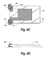
- FIG. 4C is a plan view of crystal resonator blank of FIG. 4B .
- FIG. 4D is a cross-sectional view of the crystal resonator blank of FIG. 4C , taken along line 4 D- 4 D′.
- FIG. 5A is a cross-sectional view of packaged crystal-based oscillator circuit, according to embodiments of the invention.
- FIG. 5B is a cross-sectional view of packaged crystal-based oscillator circuit with built-in inductor, according to embodiments of the invention.
- FIG. 6A illustrates a cross-section of an inductor formed in a cap of a packaged oscillator circuit, according to an embodiment of the present invention.
- FIG. 6B illustrates a cross-section of an inductor patterned along a sidewall and top surface of a cavity within a packaged oscillator circuit, according to an embodiment of the present invention.
- FIG. 7 is a three-dimensional perspective view of an electrically insulating cap having a recess therein containing a patterned inductor, according to an embodiment of the invention.
- first, second, third, etc. may be used herein to describe various elements, components, regions, layers and/or sections, these elements, components, regions, layers and/or sections should not be limited by these terms. These terms are only used to distinguish one element, component, region, layer or section from another region, layer or section. Thus, a first element, component, region, layer or section discussed below could be termed a second element, component, region, layer or section without departing from the teachings of the present invention.
- methods of forming crystal-based oscillator circuits using wafer-scale fabrication techniques include: assembling resonator blanks at wafer scale 100 a ; preparing an integrated circuit (IC) wafer for crystal (XTAL) attachment 100 b ; preparing a capping wafer 100 c ; and performing wafer scale packaging of the IC wafer 100 d .
- operations to assemble resonator blanks at wafer scale 100 a may include cutting a bar of quartz into a plurality of wafers, Block 102 , which are then polished and cut into discrete resonator blanks (e.g., rectangular resonator blanks), Block 104 .
- the resonator blanks may be loaded into a quartz blank holder having a two-dimensional array of openings therein that span the active area of a semiconductor wafer.
- the quartz blank holder may include a nest, which is sandwiched between a pair of top and bottom shadow masks, Block 106 . These shadow masks are utilized to define top and bottom electrodes on the resonator blanks. Thereafter, as shown by Block 108 , top and bottom electrode metallization (with contact metallization) is deposited onto the resonator blanks within the shadow masks, Block 108 .
- additional masks may also be used to enable the deposition of electrically conductive cement onto the contact metallization to thereby support attachment of the resonator blanks to an underlying integrated circuit wafer.
- operations to prepare an integrated circuit (IC) for crystal attachment 100 b may include forming upper level metallization and external contact pads on a passivation layer, which covers an integrated circuit wafer having crystal-oscillator circuitry embedded therein, Block 110 .
- the external contact pads may include a plurality of pads (e.g., six pads): a power supply contact pad (Vdd), a reference voltage contact pad (GND), a pair of differential periodic output signal pads OUT, OUT#, an input control voltage pad (Vcntl) and an output enable/disable pad (OE).
- the hermetic sealing material may be a eutectic alloy, which can also be deposited onto the external contact pads to enable electrical contact to corresponding through-substrate vias (within a capping wafer), as explained more fully hereinbelow.
- a sealing material may be used that does not provide a fully hermetic seal.
- the deposited sealing material may be suitable for glass frit bonding (a/k/a glass soldering, seal glass bonding), which utilizes a low melting temperature glass.
- the step of forming the upper level metallization on the passivation layer, Block 110 may also include forming crystal oscillator terminals (in pairs) thereon. Thereafter, as illustrated by Block 114 , electrode adhesion bumps (e.g., electrically conductive cement) may be deposited on the crystal oscillator terminals using, for example, screen or ink-jet printing. Other deposition techniques may also be used.
- electrode adhesion bumps e.g., electrically conductive cement
- the nested crystal resonator blanks may be mounted onto the integrated circuit wafer by contacting the electrode adhesion bumps to the top/bottom electrode contacts on the crystal resonator blanks, Block 116 .
- the electrode adhesion bumps may be contacted directly to any electrically conductive cement on the top/bottom electrode contacts.
- This use of electrically conductive cement on the top/bottom electrode contacts of the resonator blanks may be particularly advantageous for overtone-mode resonator blanks (e.g., 3 rd , 5 th overtone blanks) having sharp edges.
- the integrated circuit wafer (with resonator blanks mounted thereon) is removed from the shadow mask and the electrode adhesion bumps (e.g., conductive cement) are cured.
- the curing of the adhesion bumps may be performed as a two-step cure process performed in a vacuum.
- the first step is performed at a sufficiently high temperature to drive off volatiles in the cement and then the second step is performed at a higher temperature to increase the strength of the cement in supporting the resonator blanks.
- the contacting of the electrode adhesion bumps to the top/bottom electrode contacts, Block 116 may be performed using a pre-heated conductive cement.
- operations to prepare a capping wafer 100 c can include patterning and selectively etching deep recesses into a capping wafer, Block 122 , using, for example, deep reactive ion etching (DRIE). These recesses may be rectangular in shape and of sufficient size to fully enclose subsequently received crystal resonator blanks, which are aligned 1:1 thereto when bonded to the integrated circuit wafer. As shown by Blocks 124 - 126 , an array of through-cap openings, which may be formed to extend through the capping wafer, may be filled with through-cap electrically conductive vias/plugs.
- DRIE deep reactive ion etching
- each of the recesses in the capping wafer may be formed around of each of the recesses in the capping wafer and filled to thereby enable electrical contact to the power supply contact pad (Vdd), the reference voltage contact pad (GND), the pair of differential periodic output signal pads OUT, OUT#, the input control voltage pad (Vcntl) and the output enable/disable pad (OE).
- Vdd power supply contact pad
- GND reference voltage contact pad
- OE input control voltage pad
- OE output enable/disable pad
- four pads may be provided for signals OUT, OE, Vdd and GND, when only a single-sided output signal is required.
- the steps illustrated by Blocks 124 - 126 may actually be performed after the capping wafer and integrated circuit wafer have been bonded together.
- Materials for hermetic sealing e.g., eutectic metal
- non-hermetic sealing may be selectively deposited onto the capping wafer to support bonding operations, as explained hereinbelow, Block 128 .
- passive resonator elements e.g., inductor elements
- any material e.g., electrically insulating material
- frequency trimming e.g., mass loading
- operations to perform wafer scale packaging of the integrated circuit wafer 100 d may include bonding and sealing (e.g., hermetic or non-hermetic) the capping wafer to the integrated circuit wafer concurrently with performing vacuum evacuation of the cavities within the recesses in the capping wafer, Block 134 .
- wafer-scale frequency trimming operations may be performed on a device-by-device basis by removing electrode material from one or more of the quartz resonator blanks within the sealed recesses within the capping wafer or depositing material (e.g., insulating material or thinly deposited metal (e.g., Au)) onto the resonator blanks to support frequency adjustment through mass loading.
- solder bumps may be formed on the electrically conductive through-cap vias in the capping wafer before the packaged crystal-based oscillator circuits are singulated into individual circuits by dicing the capping wafer (and underlying integrated circuit wafer) along a two-dimensional grid of dicing streets extending between the hermetically-sealed recesses within the capping wafer.
- the resonator blanks with top/bottom electrode metallization may be configured as illustrated by FIGS. 2A-2C .
- a quartz resonator blank 20 may include a top electrode and contact 22 thereon, which is smaller in length and width dimensions relative to a bottom electrode 24 b (with top-side bottom electrode contact 24 a ).
- FIG. 2B illustrates a quartz resonator blank 20 having a top electrode and contact 22 thereon, which is equivalent in dimensions relative to a bottom electrode 24 b (with top-side bottom electrode contact 24 a ).
- FIG. 2A a quartz resonator blank 20 may include a top electrode and contact 22 thereon, which is smaller in length and width dimensions relative to a bottom electrode 24 b (with top-side bottom electrode contact 24 a ).
- FIG. 2B illustrates a quartz resonator blank 20 having a top electrode and contact 22 thereon, which is equivalent in dimensions relative to a bottom electrode 24 b (with top-side bottom electrode contact 24 a ).
- FIG. 2C illustrates a quartz resonator blank 20 having a top electrode 22 ′ with diagonally opposite contacts and a bottom electrode 24 b ′ with diagonally opposite top-side contacts 24 a ′, which enable multiple orientations (e.g., 180° rotations) of the blank 20 within a quartz holder prior to mounting to an integrated circuit wafer.
- FIG. 3A illustrates a wafer-scale quartz blank holder 30 having a two-dimensional array of rectangular-shaped openings 32 therein, which have sufficient size to retain quartz crystal blanks therein, as illustrated by FIG. 3D .
- FIG. 3B is a bottom-up view of a bottom electrode shadow mask mounted to the quartz blank holder of FIG. 3A .
- This bottom electrode shadow mask includes patterned openings 34 therein that are aligned to each opening 32 within the blank holder 30 and support formation of bottom electrodes on quartz blanks held within the openings 32 .
- the patterned openings 34 are sufficiently large that they extend outside the dimensions of the openings 32 in the blank holder 30 .
- FIG. 3C is a top-down view of a top electrode shadow mask mounted to the quartz blank holder of FIG. 3A .
- This top electrode shadow mask includes patterned openings 36 therein that are aligned to each opening 32 within the blank holder 30 and support formation of top electrodes (and top/bottom electrode contacts) on quartz blanks held within the openings 32 .
- the patterned openings 36 are sufficiently large that they extend outside the dimensions of the openings 32 in the blank holder 30 .
- FIG. 3D illustrates a cross-sectional view of a portion of the double-sided shadow mask of FIGS. 3A-3C having a quartz blank holder 30 nested therein.
- the quartz blank holder 30 may be permanently mounted to one of the top and bottom shadow masks, but the top and bottom shadow masks may be held in a fixed position relation relative to each other using an array of magnets 35 , which operate to hold at least one shadow masks against the quartz blank holder 30 when populated with quartz blanks 20 .
- FIGS. 4A-4B an integrated circuit wafer having a two-dimensional array of oscillator circuits 40 therein is illustrated as including respective pairs of electrode adhesion bumps 26 a , 26 b (e.g., electrically conductive cement) on a surface thereof. These adhesion bumps 26 a , 26 b may be formed as described hereinabove with respect to Block 114 in FIG. 1A .
- FIG. 4B is an enlarged view of a portion the integrated circuit wafer of FIG. 4A , after crystal resonator blanks 20 have been mounted thereon as disclosed above with respect to Blocks 116 - 120 in FIG. 1A .
- the electrode adhesion bumps 26 a , 26 b may be configured to provide electrical contact to the top and bottom electrodes ( 22 , 24 a - 24 b ) associated with each resonator blank 20 and support each resonator blank 20 at a fixed distance above a surface of an underlying oscillator circuit 40 (e.g., above a surface of a passivation layer overlying an oscillator circuit embedded within a silicon substrate).
- FIGS. 5A-5B illustrate packaged crystal-based oscillator circuits, which may be finalized as described hereinabove with respect to FIG. 1C and possibly using one or more steps described in U.S. Pat. No. 7,955,885 to Bhugra et al., the disclosure of which is hereby incorporated herein by reference.
- the packaged oscillator circuit includes an integrated circuit substrate 40 (e.g., silicon die), which has oscillator circuitry therein, and a cap 42 (e.g., silicon cap), which is hermetically bonded to the substrate 40 (e.g., using a eutectic alloy).
- each singulated cap 42 includes a recess 44 and cavity 46 therein, which houses a resonator blank 20 .
- This resonator blank 20 is mounted and electrically connected to the underlying substrate 40 by the electrically conductive adhesion bumps 26 a , 26 b .
- Electrically conductive through-cap vias (not shown) electrically connect solder bumps 50 to corresponding pads on the substrate 40 in the embodiment of FIG. 5A . In FIG. 5B , the solder bumps 50 are directly connected to the substrate 40 .
- the recess 44 within the cap 42 may also include a deposited material layer 48 , which can be partially transferred to the resonator blank 20 (as mass loading) during an electrical trimming operation.
- This electrical trimming operation may be performed before and/or after the singulation of the packaged integrated circuit wafer.
- the material layer 48 may be an electrically conductive layer that is formed by removing electrode material from the resonator blank 20 during electrical trimming.
- FIG. 5B illustrates the presence of an inductor 52 on a surface of the substrate 40 . As shown, at least a portion of this inductor 52 (e.g., spiral inductor) may be disposed between the resonator blank 20 and the substrate 40 .
- the inductor 52 may be disposed on an upper passivation layer, which covers the substrate 40 .
- this passivation layer may contain a magnetically reflective layer (e.g., M1 metal layer) that inhibits a reduction in inductor Q caused by the underlying “lossy” substrate.
- an inductor 52 may be configured with vertical through-cap vias 52 a (TCVs) and planar segments 52 b , 52 c that are serially connected together, with segments 52 b extending on an outside top surface of a cap 42 of a packaged oscillator circuit and segments 52 c extending between a bottom surface of the cap 42 and underlying IC passivation layers 40 b , which extend on an uppermost surface (e.g., active circuit surface) of an underlying integrated circuit chip 40 a within an integrated circuit substrate 40 .
- a centermost bottom segment 52 c may be utilized as a center-tap (CT) of the inductor 52 in some embodiments of the invention.
- the inductor 52 ′ of FIG. 6B replaces the TCVs 52 a of FIG. 6A with inductor segments 52 a ′, 52 b ′, which are patterned on a sidewall and top inner surface of a recess 44 within the cap 42 , respectively.
- the segments 52 b ′ are arcuate-shaped (e.g., circular) inductor segments that are joined at a center tap (CT) of the inductor 52 ′ and the outermost sidewall segments 52 a ′ are electrically connected to lateral segments 52 c , which extend between a bottom surface of the cap 42 and the underlying IC passivation layers 40 b.
- CT center tap
- an electrically insulating cap 70 e.g., glass cap
- a recess therein having a plurality of sidewalls 78 a , an interior top surface 78 b within the recess and a primary/bonding surface 78 c containing a metal seal ring 74 with tie bar extensions 74 a on each side thereof.
- a center-tap inductor 76 is patterned to extend on each of the interior top surface 78 b , sidewall 78 a and bonding surface 78 c .
- the inductor 76 may include a pair of arcuate-shaped segments, which may be mirror-images of each other about a center tap. Preferably, these arcuate-shaped segments have rounded corners and may even be semicircular-shaped.
- a center tap 76 a of the inductor 76 may be provided, which is electrically connected to the metal seal ring 74 . This metal seal ring 74 may be held at a fixed potential (e.g., GND) during operation of a packaged integrated circuit.
- the cap 70 may include a magnetic material therein, which increases an effective inductance of the inductor 76 relative to an otherwise equivalent cap and inductor combination that is devoid of the magnetic material, such as a ferrous-type material or a magnetic rare-earth material.
- methods of forming the electrically insulating cap 70 of FIG. 7 may utilize wafer-scale fabrication techniques, which can include providing a glass plate having a two-dimensional array of recesses ( 78 a , 78 b ) therein and then plating a relatively thin electrically conductive material (e.g., copper (Cu)) and possibly an adhesion layer using an electroless plating bath, for example.
- a relatively thin electrically conductive material e.g., copper (Cu)
- this plating step if used, may be selective to the non-recess side of the glass plate/wafer.
- the shape of the center-tap inductor 76 within each of the recesses may be defined by performing deep resolution photoresist and patterning steps on the electrically conductive material.
- an electroplating step may be performed to selectively thicken the inductor pattern, using tie bars and seal rings ( 74 , 74 a ) to provide a necessary electrical connection between all recesses on the plate.
- this electroplating step may utilize a combination of copper (Cu) followed by a low temperature eutectic solder (e.g., AuSn) to enable sealing of the seal rings 74 to a similarly patterned connection material in an underlying integrated circuit wafer, prior to dicing.
- Cu copper
- AuSn low temperature eutectic solder
Abstract
Description
Claims (15)
Priority Applications (4)
| Application Number | Priority Date | Filing Date | Title |
|---|---|---|---|
| US14/136,040 US9397151B1 (en) | 2013-08-30 | 2013-12-20 | Packaged integrated circuits having high-Q inductors therein and methods of forming same |
| US14/586,534 US9445536B1 (en) | 2013-08-30 | 2014-12-30 | Crystal oscillator fabrication methods using dual-deposition of mounting cement and dual-curing techniques |
| US14/586,525 US9478599B1 (en) | 2013-08-30 | 2014-12-30 | Integrated circuit device substrates having packaged inductors thereon |
| US14/586,508 US9306537B1 (en) | 2013-08-30 | 2014-12-30 | Integrated circuit device substrates having packaged crystal resonators thereon |
Applications Claiming Priority (2)
| Application Number | Priority Date | Filing Date | Title |
|---|---|---|---|
| US201314015471A | 2013-08-30 | 2013-08-30 | |
| US14/136,040 US9397151B1 (en) | 2013-08-30 | 2013-12-20 | Packaged integrated circuits having high-Q inductors therein and methods of forming same |
Publications (1)
| Publication Number | Publication Date |
|---|---|
| US9397151B1 true US9397151B1 (en) | 2016-07-19 |
Family
ID=56381746
Family Applications (2)
| Application Number | Title | Priority Date | Filing Date |
|---|---|---|---|
| US14/136,040 Active 2034-05-22 US9397151B1 (en) | 2013-08-30 | 2013-12-20 | Packaged integrated circuits having high-Q inductors therein and methods of forming same |
| US14/586,525 Active US9478599B1 (en) | 2013-08-30 | 2014-12-30 | Integrated circuit device substrates having packaged inductors thereon |
Family Applications After (1)
| Application Number | Title | Priority Date | Filing Date |
|---|---|---|---|
| US14/586,525 Active US9478599B1 (en) | 2013-08-30 | 2014-12-30 | Integrated circuit device substrates having packaged inductors thereon |
Country Status (1)
| Country | Link |
|---|---|
| US (2) | US9397151B1 (en) |
Cited By (4)
| Publication number | Priority date | Publication date | Assignee | Title |
|---|---|---|---|---|
| CN106409808A (en) * | 2016-11-23 | 2017-02-15 | 无锡吉迈微电子有限公司 | Three-dimensional spiral inductor |
| US20170166442A1 (en) * | 2015-12-11 | 2017-06-15 | Integrated Device Technology, Inc. | System and method for providing hermetically sealed packages with consistent vacuum cavity |
| WO2019089150A1 (en) * | 2017-10-30 | 2019-05-09 | Qualcomm Incorporated | Integration of through glass via (tgv) filter and acoustic filter |
| US20210028077A1 (en) * | 2018-04-03 | 2021-01-28 | Corning Incorporated | Hermetically sealed optically transparent wafer-level packages and methods for making the same |
Families Citing this family (5)
| Publication number | Priority date | Publication date | Assignee | Title |
|---|---|---|---|---|
| FR3046701B1 (en) * | 2016-01-08 | 2018-03-23 | Commissariat A L'energie Atomique Et Aux Energies Alternatives | NETWORK ANTENNA, IN PARTICULAR FOR NUCLEAR MAGNETIC RESONANCE IMAGING, COMPRISING LINEAR ELECTROMAGNETIC RESONATORS AND AT LEAST ONE DECOUPLING DEVICE |
| US10910325B2 (en) * | 2017-05-29 | 2021-02-02 | Intel Corporation | Integrated circuit packages with conductive element having cavities housing electrically connected embedded components |
| CN107481997A (en) * | 2017-09-05 | 2017-12-15 | 中国电子科技集团公司第二十九研究所 | A kind of double stacked level Hermetic Package structure and method |
| CN110676244B (en) * | 2019-10-15 | 2020-06-16 | 杭州见闻录科技有限公司 | Chip packaging method and packaging structure |
| US20210376816A1 (en) * | 2020-05-29 | 2021-12-02 | RF360 Europe GmbH | Package comprising stacked filters |
Citations (28)
| Publication number | Priority date | Publication date | Assignee | Title |
|---|---|---|---|---|
| US5577319A (en) | 1995-03-31 | 1996-11-26 | Motorola, Inc. | Method of encapsulating a crystal oscillator |
| US5702775A (en) | 1995-12-26 | 1997-12-30 | Motorola, Inc. | Microelectronic device package and method |
| US5815054A (en) | 1997-05-27 | 1998-09-29 | Motorola Inc. | Surface micromachined acoustic wave piezoelectric crystal with electrodes on raised ridges and in spaces therebetween |
| US6114937A (en) * | 1996-08-23 | 2000-09-05 | International Business Machines Corporation | Integrated circuit spiral inductor |
| US6635949B2 (en) * | 2002-01-04 | 2003-10-21 | Intersil Americas Inc. | Symmetric inducting device for an integrated circuit having a ground shield |
| US6759727B2 (en) * | 1999-08-23 | 2004-07-06 | Hynix Semiconductor Inc. | Inductor and fabricating method thereof |
| US6786654B2 (en) * | 2002-08-21 | 2004-09-07 | Hymite A/S | Encapsulated optical fiber end-coupled device |
| US6798039B1 (en) | 2002-10-21 | 2004-09-28 | Integrated Device Technology, Inc. | Integrated circuit inductors having high quality factors |
| US20050258507A1 (en) * | 2004-05-21 | 2005-11-24 | Taiwan Semiconductor Manufacturing Co. Ltd. | Q-factor with electrically controllable resistivity of silicon substrate layer |
| US20060016065A1 (en) | 2000-07-17 | 2006-01-26 | Yoshiaki Nagaura | Piezoelectric device and acousto-electric transducer and method for manufacturing the same |
| US6998925B2 (en) * | 2002-07-15 | 2006-02-14 | Nihon Dempa Kogyo Co., Ltd. | Surface-mount crystal oscillator |
| US20070085648A1 (en) * | 2005-10-19 | 2007-04-19 | Samsung Electronics Co., Ltd. | High efficiency inductor, method for manufacturing the inductor, and packaging structure using the inductor |
| US7291513B2 (en) | 2003-12-15 | 2007-11-06 | Dalsa Semiconductor Inc. | Hermetic wafer-level packaging for MEMS devices with low-temperature metallurgy |
| US20080042260A1 (en) * | 2006-08-21 | 2008-02-21 | Jeong Heewon | Micro-electromechanical systems device and manufacturing method thereof |
| US20080231145A1 (en) | 2007-03-22 | 2008-09-25 | Epson Toyocom Corporation | Quartz crystal device and method for sealing the same |
| US20090015363A1 (en) * | 1999-11-23 | 2009-01-15 | Gardner Donald S | Integrated transformer |
| US7605521B2 (en) | 2006-01-10 | 2009-10-20 | Epson Toyocom Corporation | Hermetically sealed structure, piezoelectric device and improvement of method for manufacturing the same |
| US7875955B1 (en) * | 2006-03-09 | 2011-01-25 | National Semiconductor Corporation | On-chip power inductor |
| US7955885B1 (en) | 2009-01-09 | 2011-06-07 | Integrated Device Technology, Inc. | Methods of forming packaged micro-electromechanical devices |
| US8035454B2 (en) | 2009-03-09 | 2011-10-11 | Micro Crystal Ag | Oscillator device comprising a thermally-controlled piezoelectric resonator |
| US8044755B2 (en) * | 2008-04-09 | 2011-10-25 | National Semiconductor Corporation | MEMS power inductor |
| US20120056510A9 (en) | 2009-03-31 | 2012-03-08 | Sand9, Inc. | Integration of piezoelectric materials with substrates |
| US8164159B1 (en) | 2009-07-18 | 2012-04-24 | Intergrated Device Technologies, inc. | Semiconductor resonators with electromagnetic and environmental shielding and methods of forming same |
| US8294260B2 (en) | 2005-06-08 | 2012-10-23 | Seiko Epson Corporation | Semiconductor device, manufacturing method for semiconductor device, electronic component, circuit substrate, and electronic apparatus |
| US8466537B1 (en) * | 2011-12-30 | 2013-06-18 | Texas Instruments Incorporated | MEMS power inductor with magnetic laminations formed in a crack resistant high aspect ratio structure |
| US8476810B2 (en) | 2010-01-05 | 2013-07-02 | Seiko Epson Corporation | Piezoelectric device and piezoelectric device manufacturing method |
| US8482358B2 (en) | 2010-07-09 | 2013-07-09 | Seiko Epson Corporation | Flexural resonator element, resonator, oscillator, and electronic device |
| US20130335157A1 (en) * | 2012-06-13 | 2013-12-19 | Seiko Epson Corporation | Resonating element, resonator, electronic device, electronic apparatus, and moving body |
Family Cites Families (7)
| Publication number | Priority date | Publication date | Assignee | Title |
|---|---|---|---|---|
| KR100300527B1 (en) * | 1998-09-03 | 2001-10-27 | 윤덕용 | Remote pressure monitoring device of sealed type and manufacture method for the same |
| US6384473B1 (en) * | 2000-05-16 | 2002-05-07 | Sandia Corporation | Microelectronic device package with an integral window |
| US7034441B2 (en) | 2002-11-13 | 2006-04-25 | Nihon Dempa Kogyo Co., Ltd | Surface mount crystal unit and surface mount crystal oscillator |
| WO2007131967A1 (en) * | 2006-05-15 | 2007-11-22 | Koninklijke Philips Electronics N.V. | Integrated low-loss capacitor-arrray structure |
| JP2009065334A (en) | 2007-09-05 | 2009-03-26 | Nippon Dempa Kogyo Co Ltd | Surface-mount crystal oscillator |
| JP2012169862A (en) * | 2011-02-14 | 2012-09-06 | Seiko Instruments Inc | Crystal device, manufacturing method of the crystal device, piezoelectric transducer, oscillator, electronic apparatus, and atomic clock |
| JP6146313B2 (en) * | 2011-12-05 | 2017-06-14 | パナソニックIpマネジメント株式会社 | Wireless module |
-
2013
- 2013-12-20 US US14/136,040 patent/US9397151B1/en active Active
-
2014
- 2014-12-30 US US14/586,525 patent/US9478599B1/en active Active
Patent Citations (30)
| Publication number | Priority date | Publication date | Assignee | Title |
|---|---|---|---|---|
| US5577319A (en) | 1995-03-31 | 1996-11-26 | Motorola, Inc. | Method of encapsulating a crystal oscillator |
| US5702775A (en) | 1995-12-26 | 1997-12-30 | Motorola, Inc. | Microelectronic device package and method |
| US5928598A (en) | 1995-12-26 | 1999-07-27 | Motorola, Inc. | Method of making a microelectronic device package |
| US6114937A (en) * | 1996-08-23 | 2000-09-05 | International Business Machines Corporation | Integrated circuit spiral inductor |
| US5815054A (en) | 1997-05-27 | 1998-09-29 | Motorola Inc. | Surface micromachined acoustic wave piezoelectric crystal with electrodes on raised ridges and in spaces therebetween |
| US6759727B2 (en) * | 1999-08-23 | 2004-07-06 | Hynix Semiconductor Inc. | Inductor and fabricating method thereof |
| US20090015363A1 (en) * | 1999-11-23 | 2009-01-15 | Gardner Donald S | Integrated transformer |
| US20060016065A1 (en) | 2000-07-17 | 2006-01-26 | Yoshiaki Nagaura | Piezoelectric device and acousto-electric transducer and method for manufacturing the same |
| US6635949B2 (en) * | 2002-01-04 | 2003-10-21 | Intersil Americas Inc. | Symmetric inducting device for an integrated circuit having a ground shield |
| US6998925B2 (en) * | 2002-07-15 | 2006-02-14 | Nihon Dempa Kogyo Co., Ltd. | Surface-mount crystal oscillator |
| US6786654B2 (en) * | 2002-08-21 | 2004-09-07 | Hymite A/S | Encapsulated optical fiber end-coupled device |
| US6798039B1 (en) | 2002-10-21 | 2004-09-28 | Integrated Device Technology, Inc. | Integrated circuit inductors having high quality factors |
| US7291513B2 (en) | 2003-12-15 | 2007-11-06 | Dalsa Semiconductor Inc. | Hermetic wafer-level packaging for MEMS devices with low-temperature metallurgy |
| US20050258507A1 (en) * | 2004-05-21 | 2005-11-24 | Taiwan Semiconductor Manufacturing Co. Ltd. | Q-factor with electrically controllable resistivity of silicon substrate layer |
| US8294260B2 (en) | 2005-06-08 | 2012-10-23 | Seiko Epson Corporation | Semiconductor device, manufacturing method for semiconductor device, electronic component, circuit substrate, and electronic apparatus |
| US20070085648A1 (en) * | 2005-10-19 | 2007-04-19 | Samsung Electronics Co., Ltd. | High efficiency inductor, method for manufacturing the inductor, and packaging structure using the inductor |
| US7605521B2 (en) | 2006-01-10 | 2009-10-20 | Epson Toyocom Corporation | Hermetically sealed structure, piezoelectric device and improvement of method for manufacturing the same |
| US7875955B1 (en) * | 2006-03-09 | 2011-01-25 | National Semiconductor Corporation | On-chip power inductor |
| US20080042260A1 (en) * | 2006-08-21 | 2008-02-21 | Jeong Heewon | Micro-electromechanical systems device and manufacturing method thereof |
| US20120025673A1 (en) | 2007-03-22 | 2012-02-02 | Seiko Epson Corporation | Quartz crystal device and method for sealing the same |
| US20080231145A1 (en) | 2007-03-22 | 2008-09-25 | Epson Toyocom Corporation | Quartz crystal device and method for sealing the same |
| US8044755B2 (en) * | 2008-04-09 | 2011-10-25 | National Semiconductor Corporation | MEMS power inductor |
| US7955885B1 (en) | 2009-01-09 | 2011-06-07 | Integrated Device Technology, Inc. | Methods of forming packaged micro-electromechanical devices |
| US8035454B2 (en) | 2009-03-09 | 2011-10-11 | Micro Crystal Ag | Oscillator device comprising a thermally-controlled piezoelectric resonator |
| US20120056510A9 (en) | 2009-03-31 | 2012-03-08 | Sand9, Inc. | Integration of piezoelectric materials with substrates |
| US8164159B1 (en) | 2009-07-18 | 2012-04-24 | Intergrated Device Technologies, inc. | Semiconductor resonators with electromagnetic and environmental shielding and methods of forming same |
| US8476810B2 (en) | 2010-01-05 | 2013-07-02 | Seiko Epson Corporation | Piezoelectric device and piezoelectric device manufacturing method |
| US8482358B2 (en) | 2010-07-09 | 2013-07-09 | Seiko Epson Corporation | Flexural resonator element, resonator, oscillator, and electronic device |
| US8466537B1 (en) * | 2011-12-30 | 2013-06-18 | Texas Instruments Incorporated | MEMS power inductor with magnetic laminations formed in a crack resistant high aspect ratio structure |
| US20130335157A1 (en) * | 2012-06-13 | 2013-12-19 | Seiko Epson Corporation | Resonating element, resonator, electronic device, electronic apparatus, and moving body |
Non-Patent Citations (4)
| Title |
|---|
| Ruffieux et al. "A Versatile Timing Microsystem Based on Wafer-Level Packaged XTAL/BAW Resonators with Sub-muW RTC Mode and Programmable HF Clocks", 2013 IEEE International Solid-State Circuits Conference, ISSCC 2013, Feb. 19, 2013, 196-198. |
| Ruffieux et al. "A Versatile Timing Microsystem Based on Wafer-Level Packaged XTAL/BAW Resonators with Sub-μW RTC Mode and Programmable HF Clocks", 2013 IEEE International Solid-State Circuits Conference, ISSCC 2013, Feb. 19, 2013, 196-198. |
| Zoschke et al. "Hermatic Wafer Level Packaging of MEMS Components Using Through Silicon Via and Wafer to Wafer Bonding Technologies", IEEE 2013 Electronic Components & Technology Conference, 2013, 1500-1507. |
| Zoschke et al. "Hermetic Wafer Level Packaging of MEMS Components Using Through Silicon Via and Wafer to Wafer Bonding Technologies", The 63rd Electronic Components and Technology Conference, ECTC 2013, May 28-31, 2013, Las Vegas, NV, USA, 33 pages. |
Cited By (7)
| Publication number | Priority date | Publication date | Assignee | Title |
|---|---|---|---|---|
| US20170166442A1 (en) * | 2015-12-11 | 2017-06-15 | Integrated Device Technology, Inc. | System and method for providing hermetically sealed packages with consistent vacuum cavity |
| CN106409808A (en) * | 2016-11-23 | 2017-02-15 | 无锡吉迈微电子有限公司 | Three-dimensional spiral inductor |
| CN106409808B (en) * | 2016-11-23 | 2019-04-16 | 厦门云天半导体科技有限公司 | Three-dimensional spiral inductance |
| WO2019089150A1 (en) * | 2017-10-30 | 2019-05-09 | Qualcomm Incorporated | Integration of through glass via (tgv) filter and acoustic filter |
| US10582609B2 (en) | 2017-10-30 | 2020-03-03 | Qualcomm Incorporated | Integration of through glass via (TGV) filter and acoustic filter |
| US20210028077A1 (en) * | 2018-04-03 | 2021-01-28 | Corning Incorporated | Hermetically sealed optically transparent wafer-level packages and methods for making the same |
| US11764117B2 (en) * | 2018-04-03 | 2023-09-19 | Corning Incorporated | Hermetically sealed optically transparent wafer-level packages and methods for making the same |
Also Published As
| Publication number | Publication date |
|---|---|
| US9478599B1 (en) | 2016-10-25 |
Similar Documents
| Publication | Publication Date | Title |
|---|---|---|
| US9397151B1 (en) | Packaged integrated circuits having high-Q inductors therein and methods of forming same | |
| US9306537B1 (en) | Integrated circuit device substrates having packaged crystal resonators thereon | |
| US10581402B1 (en) | Integrated quartz MEMS tuning fork resonator/oscillator | |
| US8991022B2 (en) | Method for manufacturing piezoelectric resonator device | |
| US9620390B2 (en) | Method of making a semiconductor device having a functional capping | |
| US9793877B2 (en) | Encapsulated bulk acoustic wave (BAW) resonator device | |
| US9431955B1 (en) | Monolithic composite resonator devices with reduced sensitivity to acceleration and vibration | |
| US20030183920A1 (en) | Hermetic electric component package | |
| US20100053922A1 (en) | Micropackaging method and devices | |
| TW201937768A (en) | Methods of manufacturing RF filters | |
| US20050073040A1 (en) | Wafer level package for micro device and manufacturing method thereof | |
| CN103413795A (en) | Semiconductor device packing structure and semiconductor device packing technological process | |
| US9718678B2 (en) | Package arrangement, a package, and a method of manufacturing a package arrangement | |
| US10312185B2 (en) | Inductively coupled microelectromechanical system resonator | |
| KR100558439B1 (en) | FBAR of Wafer Level Pakage and manufacturing method thereof | |
| US7285844B2 (en) | Multiple internal seal right micro-electro-mechanical system vacuum package | |
| TWI498951B (en) | Conductor - type package structure and its manufacturing method | |
| JP2006088268A (en) | Semiconductor device and method of manufacturing the same | |
| US9985198B1 (en) | High Q quartz-based MEMS resonators and methods of fabricating same | |
| JP4761713B2 (en) | Electronic component sealing substrate, multi-component electronic component sealing substrate, and method of manufacturing electronic device | |
| US20110068880A1 (en) | Micromechanical network | |
| US8426233B1 (en) | Methods of packaging microelectromechanical resonators | |
| US10141906B1 (en) | High Q quartz-based MEMS resonators and method of fabricating same | |
| US9445536B1 (en) | Crystal oscillator fabrication methods using dual-deposition of mounting cement and dual-curing techniques | |
| WO2022183491A1 (en) | Quartz crystal resonator and processing method therefor, and electronic device |
Legal Events
| Date | Code | Title | Description |
|---|---|---|---|
| AS | Assignment |
Owner name: INTEGRATED DEVICE TECHNOLOGY, INC., CALIFORNIA Free format text: ASSIGNMENT OF ASSIGNORS INTEREST;ASSIGNORS:ASTROF, KENNETH L.;GUBSER, ROBERT A.;GHAI, AJAY KUMAR;AND OTHERS;SIGNING DATES FROM 20140324 TO 20140325;REEL/FRAME:032531/0244 |
|
| STCF | Information on status: patent grant |
Free format text: PATENTED CASE |
|
| AS | Assignment |
Owner name: JPMORGAN CHASE BANK, N.A., AS COLLATERAL AGENT, NE Free format text: SECURITY AGREEMENT;ASSIGNORS:INTEGRATED DEVICE TECHNOLOGY, INC.;GIGPEAK, INC.;MAGNUM SEMICONDUCTOR, INC.;AND OTHERS;REEL/FRAME:042166/0431 Effective date: 20170404 Owner name: JPMORGAN CHASE BANK, N.A., AS COLLATERAL AGENT, NEW YORK Free format text: SECURITY AGREEMENT;ASSIGNORS:INTEGRATED DEVICE TECHNOLOGY, INC.;GIGPEAK, INC.;MAGNUM SEMICONDUCTOR, INC.;AND OTHERS;REEL/FRAME:042166/0431 Effective date: 20170404 |
|
| AS | Assignment |
Owner name: CHIPX, INCORPORATED, CALIFORNIA Free format text: RELEASE BY SECURED PARTY;ASSIGNOR:JPMORGAN CHASE BANK, N.A.;REEL/FRAME:048746/0001 Effective date: 20190329 Owner name: ENDWAVE CORPORATION, CALIFORNIA Free format text: RELEASE BY SECURED PARTY;ASSIGNOR:JPMORGAN CHASE BANK, N.A.;REEL/FRAME:048746/0001 Effective date: 20190329 Owner name: GIGPEAK, INC., CALIFORNIA Free format text: RELEASE BY SECURED PARTY;ASSIGNOR:JPMORGAN CHASE BANK, N.A.;REEL/FRAME:048746/0001 Effective date: 20190329 Owner name: INTEGRATED DEVICE TECHNOLOGY, INC., CALIFORNIA Free format text: RELEASE BY SECURED PARTY;ASSIGNOR:JPMORGAN CHASE BANK, N.A.;REEL/FRAME:048746/0001 Effective date: 20190329 Owner name: MAGNUM SEMICONDUCTOR, INC., CALIFORNIA Free format text: RELEASE BY SECURED PARTY;ASSIGNOR:JPMORGAN CHASE BANK, N.A.;REEL/FRAME:048746/0001 Effective date: 20190329 |
|
| MAFP | Maintenance fee payment |
Free format text: PAYMENT OF MAINTENANCE FEE, 4TH YEAR, LARGE ENTITY (ORIGINAL EVENT CODE: M1551); ENTITY STATUS OF PATENT OWNER: LARGE ENTITY Year of fee payment: 4 |
|
| MAFP | Maintenance fee payment |
Free format text: PAYMENT OF MAINTENANCE FEE, 8TH YEAR, LARGE ENTITY (ORIGINAL EVENT CODE: M1552); ENTITY STATUS OF PATENT OWNER: LARGE ENTITY Year of fee payment: 8 |