EP1541706B1 - Mecanisme de masquage destine a un dispositif de formation de films - Google Patents
Mecanisme de masquage destine a un dispositif de formation de films Download PDFInfo
- Publication number
- EP1541706B1 EP1541706B1 EP03797681A EP03797681A EP1541706B1 EP 1541706 B1 EP1541706 B1 EP 1541706B1 EP 03797681 A EP03797681 A EP 03797681A EP 03797681 A EP03797681 A EP 03797681A EP 1541706 B1 EP1541706 B1 EP 1541706B1
- Authority
- EP
- European Patent Office
- Prior art keywords
- mask
- action edge
- relative
- disk
- single action
- Prior art date
- Legal status (The legal status is an assumption and is not a legal conclusion. Google has not performed a legal analysis and makes no representation as to the accuracy of the status listed.)
- Expired - Fee Related
Links
Images


Classifications
-
- C—CHEMISTRY; METALLURGY
- C23—COATING METALLIC MATERIAL; COATING MATERIAL WITH METALLIC MATERIAL; CHEMICAL SURFACE TREATMENT; DIFFUSION TREATMENT OF METALLIC MATERIAL; COATING BY VACUUM EVAPORATION, BY SPUTTERING, BY ION IMPLANTATION OR BY CHEMICAL VAPOUR DEPOSITION, IN GENERAL; INHIBITING CORROSION OF METALLIC MATERIAL OR INCRUSTATION IN GENERAL
- C23C—COATING METALLIC MATERIAL; COATING MATERIAL WITH METALLIC MATERIAL; SURFACE TREATMENT OF METALLIC MATERIAL BY DIFFUSION INTO THE SURFACE, BY CHEMICAL CONVERSION OR SUBSTITUTION; COATING BY VACUUM EVAPORATION, BY SPUTTERING, BY ION IMPLANTATION OR BY CHEMICAL VAPOUR DEPOSITION, IN GENERAL
- C23C14/00—Coating by vacuum evaporation, by sputtering or by ion implantation of the coating forming material
- C23C14/04—Coating on selected surface areas, e.g. using masks
- C23C14/042—Coating on selected surface areas, e.g. using masks using masks
-
- C—CHEMISTRY; METALLURGY
- C23—COATING METALLIC MATERIAL; COATING MATERIAL WITH METALLIC MATERIAL; CHEMICAL SURFACE TREATMENT; DIFFUSION TREATMENT OF METALLIC MATERIAL; COATING BY VACUUM EVAPORATION, BY SPUTTERING, BY ION IMPLANTATION OR BY CHEMICAL VAPOUR DEPOSITION, IN GENERAL; INHIBITING CORROSION OF METALLIC MATERIAL OR INCRUSTATION IN GENERAL
- C23C—COATING METALLIC MATERIAL; COATING MATERIAL WITH METALLIC MATERIAL; SURFACE TREATMENT OF METALLIC MATERIAL BY DIFFUSION INTO THE SURFACE, BY CHEMICAL CONVERSION OR SUBSTITUTION; COATING BY VACUUM EVAPORATION, BY SPUTTERING, BY ION IMPLANTATION OR BY CHEMICAL VAPOUR DEPOSITION, IN GENERAL
- C23C14/00—Coating by vacuum evaporation, by sputtering or by ion implantation of the coating forming material
- C23C14/0015—Coating by vacuum evaporation, by sputtering or by ion implantation of the coating forming material characterized by the colour of the layer
-
- C—CHEMISTRY; METALLURGY
- C23—COATING METALLIC MATERIAL; COATING MATERIAL WITH METALLIC MATERIAL; CHEMICAL SURFACE TREATMENT; DIFFUSION TREATMENT OF METALLIC MATERIAL; COATING BY VACUUM EVAPORATION, BY SPUTTERING, BY ION IMPLANTATION OR BY CHEMICAL VAPOUR DEPOSITION, IN GENERAL; INHIBITING CORROSION OF METALLIC MATERIAL OR INCRUSTATION IN GENERAL
- C23C—COATING METALLIC MATERIAL; COATING MATERIAL WITH METALLIC MATERIAL; SURFACE TREATMENT OF METALLIC MATERIAL BY DIFFUSION INTO THE SURFACE, BY CHEMICAL CONVERSION OR SUBSTITUTION; COATING BY VACUUM EVAPORATION, BY SPUTTERING, BY ION IMPLANTATION OR BY CHEMICAL VAPOUR DEPOSITION, IN GENERAL
- C23C14/00—Coating by vacuum evaporation, by sputtering or by ion implantation of the coating forming material
- C23C14/04—Coating on selected surface areas, e.g. using masks
- C23C14/042—Coating on selected surface areas, e.g. using masks using masks
- C23C14/044—Coating on selected surface areas, e.g. using masks using masks using masks to redistribute rather than totally prevent coating, e.g. producing thickness gradient
-
- C—CHEMISTRY; METALLURGY
- C23—COATING METALLIC MATERIAL; COATING MATERIAL WITH METALLIC MATERIAL; CHEMICAL SURFACE TREATMENT; DIFFUSION TREATMENT OF METALLIC MATERIAL; COATING BY VACUUM EVAPORATION, BY SPUTTERING, BY ION IMPLANTATION OR BY CHEMICAL VAPOUR DEPOSITION, IN GENERAL; INHIBITING CORROSION OF METALLIC MATERIAL OR INCRUSTATION IN GENERAL
- C23C—COATING METALLIC MATERIAL; COATING MATERIAL WITH METALLIC MATERIAL; SURFACE TREATMENT OF METALLIC MATERIAL BY DIFFUSION INTO THE SURFACE, BY CHEMICAL CONVERSION OR SUBSTITUTION; COATING BY VACUUM EVAPORATION, BY SPUTTERING, BY ION IMPLANTATION OR BY CHEMICAL VAPOUR DEPOSITION, IN GENERAL
- C23C14/00—Coating by vacuum evaporation, by sputtering or by ion implantation of the coating forming material
- C23C14/22—Coating by vacuum evaporation, by sputtering or by ion implantation of the coating forming material characterised by the process of coating
- C23C14/56—Apparatus specially adapted for continuous coating; Arrangements for maintaining the vacuum, e.g. vacuum locks
Definitions
- the present invention relates to a masking mechanism or device for a film forming apparatus for the purpose of making a thin film of compositions corresponding to a ternary phase diagram.
- a combinatorial film forming apparatus makes it essential to include a means for limiting supply of materials electively to a desired portion on a substrate, a film forming means for depositing films of different kind and a structural analysis means for analyzing the structure of films of desired portion on the substrate.
- a means for limiting supply of materials electively to a desired portion on a substrate for example, an apparatus which uses a ablation laser for film deposition, is equipped with a plurality of masking units, a target switching unit, an ablation laser light lead-in unit, a substrate heating laser unit and a reflection high-energy electron diffraction (RHEED) unit.
- RHEED reflection high-energy electron diffraction
- a fluorescent material for a plasma display which is required to possess properties different from those of a conventional electron-beam excited fluorescent material, is predicted to be realized by a new material of binary or ternary system.
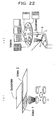
- Fig. 22 shows diagrammatically methods of investigating materials of binary and ternary systems with the conventional combinatorial deposition arrangements.
- a first mask 1 having a number of unmasking apertures for defining a plurality of independent specimens on a substrate, to wit to form pixels on the substrate and a second mask 2 in the form of a masking shield for selectively covering the unmasking apertures to select the pixels to be formed by vapor deposition.
- the relative position among the substrate, the first mask 1 and second mask 2 is adjusted to select the pixels to be formed, while a material forming the pixel by vapor deposition is selected, and this step is repeated so as to form on the substrate thin films that are of a binary or ternary phase-diagrammatic system which has predetermined ratios of components varied from pixel to pixel. Then, the pixels made are measured as to their specified properties to find out a pixel having particular properties as desired and then to determine from its ratio of components an optimum ratio of components that is required to achieve specific properties as desired.
- a rotary disk having a plurality of masks thereon, each of which are arranged to select pixels to be formed by vapor deposition, and this rotary disk is successively rotated while a material forming pixels is selected to form pixels on a substrate, which have predetermined ratios of components differing from pixel to pixel to form binary or ternary phase-diagrammatic system. Then, the pixels made are measured as to their specified properties to find out a pixel having particular properties as desired and then to determine from its ratio of components an optimum ratio of components that is required to achieve specific properties as desired.
- Fig. 23 diagrammatically shows a conventional method of making a thin film that is binary phase diagrammatic.
- a first mask 1 disposed perpendicular to a flow of vapor of material A or B and having an opening
- a second mask 2 in the form of a masking shield movable in a scanning manner parallel to the first mask 1 and a substrate disposed across the opening of the first mask 1.
- the mask 2 is moved in the direction of x while material A is being vaporized.
- This method permits obtaining a binary phase diagramming thin film in which its ratio of components continuously varies or is varied finely in the direction of x and also obtaining reliable data since the thin film can be made in an extremely short period of time.
- This method in a sense can be said to be a method of forming by uniaxial movement of a single mask having an opening relative to a substrate. Further, it can be said to be a method of forming by uniaxial movement of one side of the opening in the mask, namely uniaxial movement of a edge of the mask relative to the substrate. It will be apparent that this method can be expanded to form a ternary phase diagramming thin film by moving a mask edge triaxially or along three axes mutually intersecting at an angle of 120 degrees.
- WO 98/47613 A1 discloses an apparatus comprising a movable mask together with a rotating substrate to create a stoichiometry gradient coating.
- a masking mechanism or device for a film forming apparatus characterized in that: it comprises a single mask and a means for moving the mask relative to a substrate in a uniaxial direction; and the said mask has a first, a second and a third single action edge each of which has a normal unit vector; wherein: the normal unit vector of the said first single action edge and that of the said second single action edge make an angle of 120° relative to each other, the normal unit vector of the said second single action edge and that of the said third single action edge make an angle of 120° relative to each other, and the normal unit vector of the said third single action edge and that of the said first single action edge make an angle of 120° relative to each other.
- the first single action edge is positioned immediately ahead of a substrate region where a ternary phase diagrammatic thin film is to be formed. Then, the first single action edge may be moved at a selected rate of movement while the substrate region is vapor-deposited with a first material to produce a film thickness gradient of the first material.
- the second single action edge is positioned immediately ahead of the substrate region to be formed with the ternary phase diagrammatic thin film. Then, the second single action edge may be moved at a selected rate of movement while the substrate region is vapor-deposited with a second material to produce a film thickness gradient of the second material.
- the third single action edge is positioned immediately ahead of the substrate region to be formed with the ternary phase diagrammatic thin film.
- the third single action edge may be moved at a selected rate of movement while the substrate region is vapor-deposited with a third material to produce a film thickness gradient of the third material.
- these film thickness gradients that then develop makes 120° with one another, thereby forming a thin film of the ternary phase diagrammatic system from component thin films.
- the masking mechanism for a film forming apparatus according to the present invention entails only a single mask and a means whereby the mask can only be moved in a single axial direction and hence requires a minimum of its volume and size. With the capability of forming a thin film of a ternary phase diagrammatic system, it no longer makes it necessary to raise the equipment cost.
- single action edge is intended herein to mean an edge portion of the mask that acts to produce a film thickness gradient with one edge of the mask.
- double action edge is intended herein to mean an edge portion of the mask that acts to produce a film thickness gradient with two edges of the mask and “triple action edge” herein to mean an edge portion of the mask that acts to produce a film thickness gradient with three edges of the mask.
- the said single mask has a side making an angle of 90° + ⁇ (where 0 ° ⁇ ⁇ ⁇ 90° ) relative to the said uniaxial direction
- the said mask has a first and a second opening
- the said first opening has a side making an angle of 30° + ⁇ relative to the said uniaxial direction
- the said second opening has a side making an angle of - 30° + ⁇ relative to the said uniaxial direction
- the said side making an angle of 90° + ⁇ relative to said uniaxial direction constitutes the said first single action edge
- the said side making an angle of 30° + ⁇ relative to the said uniaxial direction constitutes the said second single action edge
- the said side making an angle of - 30° + ⁇ relative to the said uniaxial direction constitutes the said third single action edge.
- the said single mask may specifically comprise a single disk. Then, this disk has a first, a second and a third cutout, and the said first cutout has a side making an angle of 90° + ⁇ (where 0° ⁇ ⁇ ⁇ 90° ) relative to a circumferential direction of the said disk, the said second cutout has a side making an angle of 30° + ⁇ relative to the circumferential direction of the said disk and the said third cutout has a side making an angle of - 30° + ⁇ relative to the said circumferential direction of the said disk, wherein the said side making an angle of 90° + ⁇ relative to the circumferential direction of the said mask constitutes the said first single action edge, the said side making an angle of 30° + ⁇ relative to the circumferential direction of said disk constitutes the said second single action edge, and the said side making an angle of - 30° + ⁇ relative to the circumferential direction of the said disk constitutes the said third single action edge.
- This disk can be rotated about its center
- the present invention also provides in a second form of implementation thereof a masking mechanism or device for a film forming apparatus, characterized in that it comprises a single mask and a means for moving the mask relative to a substrate in a uniaxial direction; and the said mask has a first and a second single action edge and a double action edge in the form of a triangle having its base oriented in the said uniaxial direction and its two other sides constituting action edges, wherein the normal unit vector of the said first single action edge makes an angle of 30° relative to the said uniaxial direction and the normal unit vector of the said second single action edge makes - 30° relative to the said uniaxial direction.
- the first single action edge is positioned immediately ahead of a region on a substrate where a ternary phase diagrammatic thin film is to be formed. Then, the first single action edge may be moved at a selected rate of movement while the substrate region is vapor-deposited with a first material to produce a film thickness gradient of the first material.
- the second single action edge is positioned immediately ahead of the substrate region to be formed with the ternary phase diagrammatic thin film. Then, the second single action edge may be moved at a selected rate of movement while the substrate region is vapor-deposited with a second material to produce a film thickness gradient of the second material.
- the triangular double action edge is positioned immediately ahead of the substrate region to be formed with the ternary phase diagrammatic thin film. Then, the triangular double action edge may be moved at a selected rate of movement while the substrate region is vapor-deposited with a third material to produce a film thickness gradient of the third material.
- the film thickness gradient produced by means of the triangular double action edge extends perpendicular to the direction in which the mask is moved and the film thickness gradients produced by means of the first and second single action edges make an angle of 120° with one another, thereby forming a thin film of the ternary phase diagrammatic system from component thin films.
- the masking mechanism for a film forming apparatus entails, here again, only a single mask and a means whereby the mask can only be moved in a single axial direction and hence requires a minimum of its volume and size. With the capability of forming a thin film of a ternary phase diagrammatic system, it does not make it necessary to raise the equipment cost.
- the said single mask may comprise a single disk.
- this disk has a first and a second cutout
- the said first cutout is a cutout in the form of a fan having its two sides making angles of 30° and - 30° relative to a circumferential direction of the said disk, respectively
- the said second cutout is a cutout having sides making angles of 60° and - 60° relative to the circumferential direction of the said disk, respectively, and a side oriented parallel to the said circumferential direction.
- the present invention also provides in a third form of implementation thereof a masking mechanism or device for a film forming apparatus, characterized in that : it comprises a single mask and a means for moving the mask relative to a substrate in a uniaxial direction; and the said mask has a triangular opening having a base side oriented in a said uniaxial direction, the said mask also having a side extending orthogonal to the said uniaxial direction; and the other two sides other than the base side of the said triangular opening and the said side orthogonal to the said uniaxial direction constitute a triple action edge, whereby selecting a rate of movement at which the said triangular opening is moved and a rate of movement at which the said side orthogonal to the said uniaxial direction allows a film thickness gradient to be produced in a particular direction determined by the rates of movement selected.
- the triangular opening is positioned immediately ahead of a region on a substrate where a ternary phase diagrammatic thin film is to be formed. Then, the triangular opening may be moved at a selected rate of movement while the substrate region is vapor-deposited with a first material. When the triangular opening has passed over the substrate region to be formed with the ternary phase diagrammatic thin film and the said side orthogonal to the said uniaxial direction is positioned immediately ahead of the said substrate region, the rate of movement is suitably altered.
- the film thickness gradient can be produced by a desired direction by suitably selecting these rate of movement.
- the two rates of movement can suitably be selected so that the directions in which the film thickness gradients are produced for the first, second and third materials make an angle of 120° with one another, thereby forming a thin film of the ternary phase diagrammatic system desired.
- the masking mechanism for a film forming apparatus entails, here again, only a single mask and a means whereby the mask can only be moved in a single axial direction and hence requires a minimum of its volume and size. With the capability of forming a thin film of a ternary phase diagrammatic system, it does not make it necessary to raise the equipment cost.
- the said single mask may comprise a single disk. Then, this disk has a first cutout, and a second cutout or a first opening; the said first cutout is a fan shaped cutout, the said second cutout is a cutout having a side extending orthogonal to a circumferential direction f the said disk, and the said first opening is a triangular opening having a base side extending parallel to a circumferential direction of the said disk; and the two sides of the said fan shaped cutout and the side of the said second cutout that extends orthogonal to a circumferential direction of the said disk constitutes the said triple action edge, or the two sides of the said triangular opening other than the said base side and the side of the said second cutout that extends orthogonal to a circumferential direction of the said disk constitutes the said triple action edge.
- the rate of rotation of the disk can suitably be selected corresponding to the said rates of displacement so that the directions in which the film thickness gradients are produced respectively for a first, a second and a third material, thereby forming a thin film of a ternary phase diagrammatic system as desired.
- the direction in which a film thickness gradient is produced can be selected as desired, it is possible to form a thin film not only of a ternary phase diagrammatic system but also of a more than three components, multi-component phase diagrammatic system.
- the components that make up the ternary system are deposited successively on a common region on a substrate to form their respective thin films successively on this region while controlling the respective directions in which their thickness gradients are to develop and this laminating step is repeated several times until the deposited thin films in combination as a thin film of the ternary phase diagrammatic system have a desired thickness.
- the component thin films are vapor-deposited each in a layer thin enough that at the time they can be superimposed on one another by vapor deposition, their materials can mutually diffuse from one layer to another to be arranged with free energy minimum. Also, a maximum thickness ratio of the component thin films is taken corresponding to the ratio of concentration, which is equal to 1, of the components in the ternary phase-diagrammatic system. While these premises are not mentioned repetitiously hereinafter, it should be understood that they always apply. Accordingly, also the term "thin film of a ternary phase diagrammatic system" when used herein is intended to mean a thin film constructed as mentioned above, namely the realization of a ternary system in its phase diagram in the form of a thin film.
- the particular constituent composition at a given position in such a thin film can be known from its coordinates, and measuring a value of a property specified for each of given coordinate positions in the thin film to determine a coordinate position that exhibits an optimum value of the property allows a particular constituent composition that realizes optimally the desired property identified and known.
- Fig. 1 is a diagram illustrating the makeup of a masking mechanism 10 for a film forming apparatus that represents a first form of implementation of the present invention.
- the masking mechanism 10 comprises a mask 11 supported so it can be moved back and forth linearly as indicated by the arrow A on or above a substrate 12.
- the mask 11 has a side 11a and is formed with openings 11d and 11e which have sides 11b and 11c, respectively, the sides 11a, 11b and 11c here constituting action edges each of which (hereinafter referred to as a "single action edge") acts to determine a thickness gradient of a thin film to be vapor-deposited.
- the single action edges 11a, 11b and 11c have their lengths each of which is sufficiently large relative to a region of equilateral triangle 12a in the substrate 12 on which a thin film of ternary phase-diagrammatic system is to be formed.
- a single action edge generally acts in a way as described below to develop a concentration gradient of the thin film when it is vapor-deposited on the substrate 12.
- Fig. 2 is a diagram that generally represents a single action edge in a coordinate system in which the mask 11 has its face lying in an x-y plane and has its depth extending in the direction of a z-axis.
- the single action edge designated by reference character 20
- a vector d is shown as a normal unit vector of the single action edge 20 facing its mask opening side.
- Fig. 3 is a diagram illustrating an effective movement of the single action edge 20 of Fig. 2 that occurs when the mask is moved in a direction as desired.
- the moving vector of the single action edge 20 is assumed to be m. Moving the mask edge 20 with the moving vector m above the substrate 12 during its vapor deposition will cause the single action edge 20 to produce a maximum film thickness gradient in the direction of its normal vector d.
- three film thickness contours indicated by three types of dotted lines in the Figure can be considered as developing.
- the dotted lines which are the highest, the lowest and the medium in dot density are shown corresponding to the thickness contours which are the largest, the smallest and the medium in film thickness, respectively. Therefore, for any moving vector m, the inner vector product m • d comes to represent an effective amount of movement which relates to the direction in which the film thickness gradient is the maximum or is thus an effective movement (hereinafter referred to as such).
- Fig. 4 illustrates in cross sectional views typically how a thin film is grown changing its thickness profile with a single action edge of a mask when the mask is moved in moving vector +m or -m. It shows a process in which a thin film is being formed while the single action edge 20 of the mask is having a movement + m or - m. From the Figure in which the arrow ⁇ indicates a material being vapor deposited, it is seen that the thickness gradient of a thin film that develops does not depend on the direction in which the mask is moved.
- Fig. 5 is a graph illustrating a thickness profile function of a thin film formed by means of a single action edge.
- the abscissa axis is taken to lie in the direction of normal vector d of the single action edge where the vapor-deposited substrate face and the mask face lie parallel to the x-y plane while the z-axis (ordinate axis) is taken to lie in the direction of the film thickness.
- Figs. 6 , 7 and 8 are diagrams illustrating patterns of thickness gradient which develop in the thin film by means of the single action edges 11a, 11b and 11c in the masking mechanism 10 in Fig. 1 , respectively.
- a ternary phase diagram is formed in the shape of an equilateral triangle having one side perpendicular to the direction in which the mask is moved.
- the single action edges 11a, 11b and 11c have their respective normal vectors which are expressed by column vectors in equations below, respectively.
- d 1 0
- d - 1 2 - 3 2
- d - 1 2 - 3 2
- Fig. 6 diagrammatically shows thickness profile function z in the case of the single action edge 11a
- (a) indicates the film thickness expressed by equation (5) with the darkness in black color (the darker in black color the thicker is the film and the less dark in black color the thinner is the film), there being also indicated by vector B the direction in which the film thickness becomes progressively thicker.
- Diagram (b) indicates the orientation of the single action edge 11a relative to the equilateral triangular substrate region 13, there being also indicated by the white arrow the direction in which the single action edge 11b is moved.
- Fig. 7 likewise diagrammatically shows thickness profile function z in the case of the single action edge 11b wherein (a) indicates the film thickness expressed by equation (5) with the darkness in black color, there being also indicated by vector C the direction in which the film thickness becomes progressively thicker. Diagram (b) indicates the orientation of the single action edge 11b relative to the equilateral triangular substrate region 13, there being also indicated by the white arrow the direction in which the single action edge 11b is moved.
- Fig. 8 diagrammatically shows thickness profile function z in the case of the single action edge 11c wherein (a) indicates the film thickness expressed by equation (5) with the darkness in black color, there being also indicated by vector D the direction in which the film thickness becomes progressively thicker. Diagram (b) indicates the orientation of the single action edge 11c relative to the equilateral triangular substrate region 13, there being also indicated by the white arrow the direction in which the single action edge 11c is moved.
- the masking mechanism 10 for a film forming apparatus as the first form of implementation of the present invention can produce thickness gradients in, or distribute a thickness gradient into, three different directions which are mutually angularly spaced apart by an angle of 120° .
- a thin film of a ternary phase-diagrammatic system can be made by using a different material for vapor deposition on a common triangular substrate region 13 for each of film forming operations by means of single action edges 11a, 11b and 11c, respectively, acting thereon.
- a mask is shown in and described above in connection with Figs. 4 and 5 as being moved stepwise to form a thin film stepwise for the sake of facilitating the understanding of its operations, it should be noted that the mask can in actual practice be moved continuously to form a thin film while changing its thickness continuously.
- the masking mechanism 10 In the search of a material using thin films of a ternary phase diagrammatic system, properties of thin films of its binary phase diagrammatic system and thin films of its single component give auxiliary but highly useful information.
- the feature of the masking mechanism 10 according to the present invention that it permits a thin film of a binary phase diagrammatic system and a thin film of a single component or a mono-film to be formed on an identical substrate on which a thin film of their ternary phase diagrammatic system is simultaneously formed is extremely useful in the search of a material by means of a thin film of a ternary phase diagrammatic system.
- Fig. 9 is a simulated picture depicting in the thickness of black color the thickness distribution of a thin film of ternary system formed on a substrate by means of the masking mechanism shown in Fig. 1 .
- Fig. 10 is a diagram illustrating in the makeup of components various regions in the thin film of ternary system shown in Fig. 9 .
- respective sets of dotted and solid lines shown parallel to each other represents respective sets of film thickness contours of the three component materials of a ternary system, indicating that there is a concentration gradient from the dotted line towards the solid line in each set.
- an equilateral triangular region 12a at the center of a substrate 12 where the concentration gradients of the three component materials overlap there is formed a thin film of the ternary phase diagrammatic system.
- equilateral triangular regions 12b, 12c and 12d which adjoin the three sides of the equilateral triangle 12a, respectively, and where the concentration gradients of two of the three component materials overlap, there are formed thin films of binary phase diagrammatic system.
- one of two materials is deposited with a constant thickness and while the other is deposited with a concentration gradient, thus giving rise to thin films of, so-called mono-gradient.
- each of two materials is deposited with a constant thickness while in regions 12n, 120 and 12p, one material is deposited with a constant thickness, thus forming so-called simple films.
- the substrate 12 during vapor deposition can have a mask 14 mounted thereon which is separate of the mask 11 and which is formed with an unmasking aperture 14a (indicated by the alternate long and short dash line in Fig. 10 ) centering around the region 12a of the substrate 12 and larger in area than the region 12a.
- the thin films in the regions 12e - 12p expose their vertical sections to where the masking edges of the mask 14 define the unmasking aperture 14a, thereby facilitating measurement of the thickness of each of thin films grown in these regions 12e - 12p.
- the relationship between the rate of vapor deposition and the film thickness, and the relationship between the film thickness and concentration for each component are known.
- These known data will then allow a second ternary phase diagrammatic film vapor-depositing operation based thereon to form a thin film precisely of a ternary phase diagrammatic system as desired. According to this method which makes only two ternary phase diagrammatic film vapor-depositing operations sufficient, the time period that need be expended for the search for a ternary material can be made short largly.
- the single action edges 11a, 11b and 11c may generally be inclined to the direction in which the mask is moved, at an angle of 90° + ⁇ ° , an angle of 30° + ⁇ ° and an angle of - 30° + ⁇ ° , respectively, where - 90 ⁇ ⁇ ⁇ 90.
- the normal unit vectors of the single action edges 11a, 11b and 11c are mutually spaced apart by an angle 120° , permitting the formation of a ternary phase diagrammatic thin film.
- a masking mechanism may alternatively be provided that comprises a disk type mask moving rotationally.
- Fig. 11 shows a rotationally moving mask in a modification of the masking mechanism shown in Fig. 1 .
- This mask designated by reference character 15, is used so it is rotated about its center O.
- the mask 15 is formed with single action edges 15a, 15b and 15c corresponding to the single action edges 11a, 11b and 11c described previously.
- the first single action edge 15a extends radially of the disk
- the single action edges 15a, 15b and 15c have their lengths each of which is chosen to be enough large compared to the equilateral triangular region 12a of a substrate 12 on which a ternary phase diagrammatic thin film is to be formed.
- Fig. 12 shows, as partially enlarged, a single action edge moving as the mask 15 is rotated.
- the single action edge e. g., 15a
- Fig. 13 is a diagram illustrating a position on a substrate 12 in both line coordinates (x, y) and polar coordinates (r, ⁇ ) with the center of rotation O as their origin. Since a film at a position which is identical in ⁇ to but different in r from another still has an identical thickness and the thickness can be found from ⁇ , the film thickness at that position can be accurately determined by converting the position in line coordinate (x, y) into polar coordinates, utilizing an equation given below.
- the center of rotation O can be assumed to be the center of the mask 15 for the single action edge 15a. And, for the single action edges 15b and 15c their effective center of rotation with the rotation of the mask 15 can be assumed to be the origin of coordinates O.
- this masking mechanism for a film forming apparatus as a second form of implementation of the present invention.
- this masking mechanism designated by reference character 30, comprises a mask 31 supported so it can be moved forth and back linearly along an axis indicated by arrow A.
- the mask 31 is formed with unmasking openings 31e and 31f.
- the opening 31e has two single action edges 31a and 31b which are designed to produce two film thickness gradients independently of each other while the opening 31f has two action edges 31c and 31d (which are collectively referred to as a double action edge) that are designed to act jointly at the same time in developing a film thickness gradient.
- the edges 31c and 31d of the double action edge extend at angles of inclination + ⁇ 2 and - ⁇ 2 to the mask movement axis A, respectively, and intersect with each other at a vertical position (as shown, lower).
- These single and double action edges 31a, 31b, 31c and 31d have their lengths each of which is chosen to be enough long compared with the equilateral triangular region 12a on of a substrate 12 on which a ternary phase diagrammatic thin film is to be formed.
- Fig. 15 is a plan view illustrating the makeup of a double action edge.
- the double action edge designated by reference character 40, comprises edges 41 and 42 having normal unit vectors d 1 and d 2 , respectively, in an xy plane and it is assumed that moving vector m is oriented in the direction of - x.
- Fig. 16 is a diagram illustrating a thickness gradient of a thin film that develops with a double action edge 40 as shown in Fig. 15 wherein (a) is a plan view of a mask having the double action edge mask and (b) is a cross sectional view of the mask taken in a direction perpendicular to that of the mask moving vector m, from which it is seen that the film thickness becomes 0 at a point of intersection of the edges 41 and 42 in the double action edge.
- FIG. 17 is a diagram illustrating a thickness gradient of a thin film that develops with a double action edge whose two edges do not intersect with each other wherein (a) is a plan view of a mask having such a double action edge and (b) is a cross sectional view of the mask taken in a direction perpendicular to that of the mask moving vector m, from which it is seen that in the case of a double action edge whose edges do not intersect, there is no point produced where the film thickness becomes 0.
- the double action edge 31c, 31d of the mask 31 can be used to produce a film thickness gradient of one component in a first direction which is perpendicular to the direction in which the mask 31 is moved and the single action edges 31a and 31b can be used to produce film thickness gradients of the other two components in a second and a third direction which are inclined at + 120° and - 120° to the first direction, respectively, to form a ternary phase diagrammatic thin film.
- a first vapor-deposition operation may be carried out to give rise to measurements of thin films then formed in those regions and then to find from these measurements the relationship between the rate of vapor deposition and the film thickness and the relationship between the film thickness and concentration for each component.
- These measured data will then allow a second ternary phase diagrammatic film vapor-depositing operation based thereon to form a thin film precisely of a ternary phase diagrammatic system as desired.
- this method which makes only two ternary phase diagrammatic film vapor-depositing operations sufficient, the time period that need be expended for the search for a ternary material can be made short largly.
- a rotationally moving mask as a modification of the mask 31 shown in Fig. 14 .
- the masking mechanism 30 is provided with the mask 31 moving linearly, as shown it may alternatively be with a disk type mask 32 moving rotationally.
- the mask 32 comprises single action edges 32a and 32b and double action edges 32c and 32d corresponding to the aforesaid single action edges 31a and 31b and double action edges 31c and 31d.
- the edges 32c and 32d in the double action edge extend inclined at angles of + ⁇ 2 and - ⁇ 2 to a circumferential direction, respectively.
- These single and double action edges 32a, 32b, 32c and 32d have their lengths each of which is chosen to be enough long compared with the equilateral triangular region 12a of a substrate 12 on which a ternary phase diagrammatic thin film is to be formed.
- the disk constituting the mask 32 have its diameter chosen large enough that changes in angular orientation of the single action edges 32a and 32b and the double action edges 32c and 32d with the rotation of the disk are minimum.
- the corrective operation of linear to polar coordinate conversion previously described in connection with Fig. 13 for the first form of implementation can be used to properly compensate for rotary movements of the mask 32.
- this masking mechanism comprises a mask 51 supported so it can be moved forth and back linearly along an axis indicated by arrow A.
- the mask 51 is formed with unmasking openings 52d, 52e and 52f, which are designed to configure a triple action edge system in which three masks act concurrently to produce a single film thickness gradient by means of a triple action edge 52 comprising edges 52a, 52b and 52c provided therein.
- edges 52a there are two edges 52a each of which extends perpendicular to the mask displacement axis A and two sets of edges 52b and 52c wherein in each set, the two edges 52b and 52c extend oppositely inclined each other at a given angle to the mask displacement axis, and intersecting to each other at a point.
- the edges 52a, 52b and 52c have their lengths each of which is chosen to be enough large compared with the equilateral triangular region 12a of a substrate 12 on which a ternary phase diagrammatic thin film is to be formed.
- moving the mask 51 along the mask movement axis A allows the edges 52a to produce a maximum film thickness gradient in the direction of the mask movement axis A and the edges 52b and 52c to produce a maximum film thickness gradient in a direction perpendicular to the mask movement axis A.
- z 1 , z 2 and z 3 are functions describing film thickness profiles produced by the edges 52a, 52b and 52c, respectively; m is movement vector of the edges 52b and 52c; m' is the moving vector of the edges 52a; and further d 1 , d 2 and d 3 are the normal unit vectors of the edges 52a, 52b and 52c, respectively, the total film thickness profile function can then be given by an expression below.
- adjusting vector magnitudes a and b by suitably selecting mask's rate of displacement m, m' allows aligning the direction of vector v in a direction desired. Since a maximum film thickness gradient develops in the direction of vector v, it is made possible to produce such a film thickness gradient in a desired direction. To wit, suitably adjusting the rate of movement of the edge 52a, m, and the rate of displacement of the edges 52b and 52c, m', it is possible to obtain a desired film thickness gradient in a desired direction. Therefore, selecting m and m' for each of components to produce film thickness gradients in directions mutually angularly spaced by an angle of 120 ° permits forming a ternary phase diagrammatic thin film using a single mask.
- Fig. 20 is a plan view illustrating another example of making a ternary phase diagrammatic thin film by means of a masking mechanism as shown in Fig. 19 .
- a mask 51 formed with a triple action edge 52 having suitably contoured is used.
- These edges are indicated by A, B1, B2, C, D, E1, E2 and F below which are indicated by arrows directions in which film thickness gradients are produced thereby, respectively, when the mask is moved along the mask movement axis A. It follows, therefore, that as shown at (b) selecting these edges sequentially allows producing desired film thickness gradients in all the directions covering from the first to fourth quadrants to form a ternary phase diagrammatic thin film.
- Fig. 21 is a plan view illustrating a modification of the masking mechanism of Fig. 19 in which the mask is constituted by a rotationally moving mask.
- the mask 53 comprises edges 53a, and edges 53b and 53c corresponding to the edges 52a and edges 52b and 52c previously described.
- the edges 53b and 53c extend inclined at angles of + ⁇ 2 and - ⁇ 2 to a circumferential direction, respectively.
- edges 53a and the edges 53b and 53c have their respective lengths each of which is chosen to be enough long compared with the equilateral triangular region 12a of a substrate 12 on which a ternary phase diagrammatic thin film is to be formed.
- the disk constituting the mask 53 have its diameter chosen large enough that changes in angular orientation of the single action edges 53a and the edges 53b and 53c with the rotation of the disk are minimum.
- the corrective operation of linear to polar coordinate conversion as in the first and second forms of implementation can be used to obtain a precision ternary phase diagrammatic thin film.
- a masking mechanism for a film forming apparatus can form a ternary phase diagrammatic thin film.
- a masking mechanism for a film forming apparatus requires that it comprise a single mask and a means for uniaxially driving the mask and hence can be made extremely small in size and volume in order to be installed in a vacuum chamber while permitting a ternary phase diagrammatic thin film to be made without raising the equipment cost.
- the use of a masking mechanism according to the present invention makes it possible to make highly reliable binary and ternary phase diagrammatic thin films in a short period of time.
Landscapes
- Chemical & Material Sciences (AREA)
- Chemical Kinetics & Catalysis (AREA)
- Engineering & Computer Science (AREA)
- Materials Engineering (AREA)
- Mechanical Engineering (AREA)
- Metallurgy (AREA)
- Organic Chemistry (AREA)
- Physical Vapour Deposition (AREA)
Abstract
Claims (7)
- Mécanisme (10) de masquage pour un appareil de formation de film, comprenant un masque unique (11) et des moyens permettant de déplacer le masque (11) par rapport à un substrat (12) dans une direction uniaxiale, caractérisé en ce que :ledit masque (11) possède un première, un deuxième et un troisième bord à action unique (11 a, 11 b, 11 c) dont chacun possèdent un vecteur unitaire normal ; etle vecteur unitaire normal dudit premier bord à action unique (11a) et celui dudit deuxième bord à action unique (11 b) forment un angle de 120° l'un par rapport à l'autre, le vecteur unitaire normal dudit deuxième bord à action unique (11 b) et celui dudit troisième bord à action unique (11c) forment un angle de 120° l'un par rapport à l'autre, et le vecteur unitaire normal dudit troisième bord à action unique (11c) et celui dudit premier bord à action unique (11 a) forment un angle de 120° l'un par rapport à l'autre.
- Mécanisme de masquage (10) pour un appareil de formation de film tel qu'énoncé dans la revendication 1, caractérisé en ce que :ledit masque (11) possède un côté formant un angle de 90° + α (où 0° ≤ α < 90°) par rapport à ladite direction uniaxiale, etledit masque (11) possède une première et une deuxième ouverture (11d, 11e), dans laquelle,ladite première ouverture (11d) possède un côté formant un angle de 30° + α par rapport à ladite direction uniaxiale et ladite deuxième ouverture (11e) possède un côté formant un angle de - 30° + α par rapport à ladite direction uniaxiale, etledit côté formant un angle de 90° + α par rapport à ladite direction uniaxiale constitue ledit premier bord à action unique (11a), ledit côté formant un angle de 30° + α par rapport à ladite direction uniaxiale constitue ledit deuxième bord à action unique (11 b), et ledit côté formant un angle de - 30° + α par rapport à ladite direction uniaxiale constitue ledit troisième bord à action unique (11c).
- Mécanisme (15) de masquage pour un appareil de formation de film, comprenant un disque unique (15) et un moyen permettant de faire tourner le disque (15) autour de son centre, caractérisé en ce que :ledit disque (15) possède une premier, une deuxième et une troisième découpes ; etladite première découpe possède un côté formant un angle de 90° + α (où 0° ≤ α < 90°) par rapport à une direction circonférentielle dudit disque, ladite deuxième découpe possède un côté formant un angle de 30° + α par rapport à la direction circonférentielle, et ladite troisième découpe possède un côté formant un angle de - 30° + α par rapport à ladite direction circonférentielle, dans lequelledit côté formant un angle de 90° + α par rapport à ladite direction circonférentielle dudit disque (15) constitue ledit premier bord à action unique (15a), ledit côté formant un angle de 30° + α par rapport à ladite direction circonférentielle constitue ledit deuxième bord à action unique (15b), et ledit côté formant un angle de - 30° + α par rapport à ladite direction circonférentielle constitue ledit troisième bord à action unique (15c).
- Mécanisme (30) de masquage pour un appareil de formation de film, comprenant un masque unique (31) et un moyen permettant de déplacer le masque (31) par rapport à un substrat (12) dans une direction uniaxiale, caractérisé en ce que :ledit masque (31) possède un premier et un deuxième bord à action unique (31a, 31b) chacun desquels possède un vecteur unitaire normal et un bord à action double (31 c, 31d) sous la forme d'un triangle dont la base est orientée dans ladite direction uniaxiale et ses deux autres côtés constituant des bords d'action, dans lequel,le vecteur unitaire normal dudit premier bord à action unique (31a) forme un angle de 30° par rapport à ladite direction uniaxiale et le vecteur unitaire normal dudit deuxième bord à action unique (31 b) forme un angle de -30° par rapport à ladite direction uniaxiale.
- Mécanisme (10) de masquage pour un appareil de formation de film comprenant un disque unique (32) et un moyen permettant de faire tourner le disque (32) autour de son centre, caractérisé en ce que :ledit disque unique (32) possède une première et une deuxième découpe ; etladite première découpe est une découpe en forme d'éventail, et ladite deuxième découpe est une découpe possédant deux côtés formant des angles de 60° et de -60° par rapport à la direction circonférentielle dudit disque et un côté orienté parallèlement à ladite direction circonférentielle.
- Mécanisme (50) de masquage pour un appareil de formation de film comprenant un masque unique (51) et un moyen permettant de déplacer le masque (51) par rapport à un substrat (12) dans une direction uniaxiale, caractérisé en ce que :ledit masque (51) possède une ouverture triangulaire (52f) possédant un côté de base orienté dans une dite direction uniaxiale, ledit masque (51) possédant également un côté s'étendant orthogonalement à ladite direction uniaxiale ; etledit moyen permettant de déplacer le masque (51) est déplacé de sorte que les deux autres côtés autres que le côté de base de ladite ouverture triangulaire et ledit côté orthogonal à ladite direction uniaxiale constituent un bord à action triple, au moyen duquella sélection d'une vitesse de déplacement à laquelle ladite ouverture triangulaire est déplacée et une vitesse de déplacement à laquelle ledit côté orthogonal à ladite direction uniaxiale permet la production d'un gradient d'épaisseur de film dans une direction particulière déterminée par les vitesses de déplacement choisies.
- Mécanisme de masquage pour un appareil de formation de film comprenant un disque unique (53) et un moyen permettant de faire tourner le disque (53) autour de son centre, caractérisé en ce que :ledit disque (53) possède une première découpe, et une deuxième découpe ou une première ouverture ;ladite première découpe est une découpe en forme d'éventail, ladite deuxième découpe est une découpe possédant un côté s'étendant orthogonalement à une direction circonférentielle dudit disque (53), et ladite première ouverture est une ouverture triangulaire possédant un côté de base s'étendant parallèlement à une direction circonférentielle dudit disque (53) ; etles deux côtés de ladite découpe en forme d'éventail et le côté de ladite deuxième découpe qui s'étend orthogonalement à une direction circonférentielle dudit disque constitue ledit bord à action triple, ou les deux côtés de ladite ouverture triangulaire autres que ledit côté de base et le côté de ladite deuxième découpe qui s'étend orthogonalement à une direction circonférentielle dudit disque constitue ledit bord à action triple.
Applications Claiming Priority (3)
| Application Number | Priority Date | Filing Date | Title |
|---|---|---|---|
| JP2002275365 | 2002-09-20 | ||
| JP2002275365 | 2002-09-20 | ||
| PCT/JP2003/011950 WO2004027107A1 (fr) | 2002-09-20 | 2003-09-19 | Mecanisme de masquage destine a un dispositif de formation de films |
Publications (3)
| Publication Number | Publication Date |
|---|---|
| EP1541706A1 EP1541706A1 (fr) | 2005-06-15 |
| EP1541706A4 EP1541706A4 (fr) | 2009-01-21 |
| EP1541706B1 true EP1541706B1 (fr) | 2012-05-30 |
Family
ID=32025027
Family Applications (1)
| Application Number | Title | Priority Date | Filing Date |
|---|---|---|---|
| EP03797681A Expired - Fee Related EP1541706B1 (fr) | 2002-09-20 | 2003-09-19 | Mecanisme de masquage destine a un dispositif de formation de films |
Country Status (5)
| Country | Link |
|---|---|
| US (2) | US20060057240A1 (fr) |
| EP (1) | EP1541706B1 (fr) |
| JP (1) | JP4168425B2 (fr) |
| KR (1) | KR100673527B1 (fr) |
| WO (1) | WO2004027107A1 (fr) |
Families Citing this family (13)
| Publication number | Priority date | Publication date | Assignee | Title |
|---|---|---|---|---|
| US20060057240A1 (en) * | 2002-09-20 | 2006-03-16 | Hideomi Koinuma | Masking mechanism for film-forming device |
| JP4766416B2 (ja) * | 2004-08-30 | 2011-09-07 | 独立行政法人科学技術振興機構 | マスキング機構及びそれを備えた成膜装置 |
| US7654816B2 (en) * | 2004-10-07 | 2010-02-02 | Hewlett-Packard Development Company, L.P. | Lithographic mask alignment |
| KR20140059225A (ko) * | 2011-08-09 | 2014-05-15 | 어플라이드 머티어리얼스, 인코포레이티드 | 조정가능한 마스크 |
| US9939412B2 (en) | 2013-02-06 | 2018-04-10 | Empire Technology Development Llc | Devices, systems, and methods for detecting odorants |
| US20160138963A1 (en) * | 2013-06-17 | 2016-05-19 | Empire Technology Development Llc | Graded films |
| US9947441B2 (en) | 2013-11-12 | 2018-04-17 | Varian Semiconductor Equipment Associates, Inc. | Integrated superconductor device and method of fabrication |
| US10158061B2 (en) * | 2013-11-12 | 2018-12-18 | Varian Semiconductor Equipment Associates, Inc | Integrated superconductor device and method of fabrication |
| KR20150071318A (ko) * | 2013-12-18 | 2015-06-26 | 삼성디스플레이 주식회사 | 유기 발광 표시 장치의 제조 방법 |
| US9804310B2 (en) * | 2015-02-17 | 2017-10-31 | Materion Corporation | Method of fabricating anisotropic optical interference filter |
| CN106637087B (zh) * | 2016-11-18 | 2019-05-17 | 上海天马微电子有限公司 | 蒸镀设备 |
| US10947617B2 (en) * | 2017-12-03 | 2021-03-16 | Shiping Cheng | Tune able masks for PVD deposit thickness uniformity management |
| CN115386833A (zh) * | 2022-10-27 | 2022-11-25 | 宁德时代新能源科技股份有限公司 | 掩膜装置及其控制方法、镀膜设备 |
Citations (1)
| Publication number | Priority date | Publication date | Assignee | Title |
|---|---|---|---|---|
| WO1998047613A1 (fr) * | 1997-04-22 | 1998-10-29 | Symyx Technologies | Systemes et procedes de synthese combinatoire de nouveaux materiaux |
Family Cites Families (10)
| Publication number | Priority date | Publication date | Assignee | Title |
|---|---|---|---|---|
| US2433635A (en) * | 1941-10-07 | 1947-12-30 | Thomas W Sukumlyn | Method of forming optical wedges on lenses and reflectors |
| US3131078A (en) * | 1958-05-21 | 1964-04-28 | Lab For Electronics Inc | Random storage |
| JPS4327926Y1 (fr) | 1966-11-15 | 1968-11-18 | ||
| JPS4934573B1 (fr) * | 1970-11-06 | 1974-09-14 | ||
| JPS4942155U (fr) * | 1972-04-24 | 1974-04-13 | ||
| JPS59153204A (ja) | 1983-02-18 | 1984-09-01 | Toyota Motor Corp | プログラマブルコントロ−ラのプログラミング方式 |
| JPS60181264A (ja) * | 1984-02-24 | 1985-09-14 | Konishiroku Photo Ind Co Ltd | 製膜方法およびその装置 |
| US6911129B1 (en) * | 2000-05-08 | 2005-06-28 | Intematix Corporation | Combinatorial synthesis of material chips |
| JP3787719B2 (ja) | 2002-07-05 | 2006-06-21 | 独立行政法人科学技術振興機構 | 3元系相図薄膜の作製方法及びそれに用いるコンビナトリアル成膜装置用マスキング機構 |
| US20060057240A1 (en) | 2002-09-20 | 2006-03-16 | Hideomi Koinuma | Masking mechanism for film-forming device |
-
2003
- 2003-09-19 US US10/528,265 patent/US20060057240A1/en not_active Abandoned
- 2003-09-19 WO PCT/JP2003/011950 patent/WO2004027107A1/fr active IP Right Grant
- 2003-09-19 KR KR1020057004832A patent/KR100673527B1/ko active IP Right Grant
- 2003-09-19 EP EP03797681A patent/EP1541706B1/fr not_active Expired - Fee Related
- 2003-09-19 JP JP2004537609A patent/JP4168425B2/ja not_active Expired - Fee Related
-
2010
- 2010-01-05 US US12/652,340 patent/US9157144B2/en not_active Expired - Fee Related
Patent Citations (1)
| Publication number | Priority date | Publication date | Assignee | Title |
|---|---|---|---|---|
| WO1998047613A1 (fr) * | 1997-04-22 | 1998-10-29 | Symyx Technologies | Systemes et procedes de synthese combinatoire de nouveaux materiaux |
Also Published As
| Publication number | Publication date |
|---|---|
| WO2004027107A1 (fr) | 2004-04-01 |
| KR100673527B1 (ko) | 2007-01-24 |
| US9157144B2 (en) | 2015-10-13 |
| US20060057240A1 (en) | 2006-03-16 |
| US20100151128A1 (en) | 2010-06-17 |
| EP1541706A1 (fr) | 2005-06-15 |
| EP1541706A4 (fr) | 2009-01-21 |
| KR20050057515A (ko) | 2005-06-16 |
| JPWO2004027107A1 (ja) | 2006-01-19 |
| JP4168425B2 (ja) | 2008-10-22 |
Similar Documents
| Publication | Publication Date | Title |
|---|---|---|
| US9157144B2 (en) | Masking mechanism for film forming apparatus | |
| Depla et al. | Magnetron sputter deposition as visualized by Monte Carlo modeling | |
| US5475218A (en) | Instrument and method for 3-dimensional atomic arrangement observation | |
| US20090139865A1 (en) | Double-layer shutter control method of multi-sputtering system | |
| US6524449B1 (en) | Method and system for producing sputtered thin films with sub-angstrom thickness uniformity or custom thickness gradients | |
| US20170167012A1 (en) | Off-axis magnetron sputtering with real-time reflection high energy electron diffraction analysis | |
| Barber et al. | High throughput thin film materials science | |
| Schwarzer | The determination of local texture by electron diffraction–a tutorial review | |
| JP2004035983A (ja) | コンビナトリアル成膜装置用マスキング機構 | |
| Moon et al. | Combinatorial synthesis of heteroepitaxial, multi-cation, thin-films via pulsed laser deposition coupled with in-situ, chemical and structural characterization | |
| Lysne et al. | Improved methods for design of PLD and combinatorial PLD films | |
| KR20010042805A (ko) | 조합 분자빔 에피탁시(combe) 장치를 사용한라이브러리의 제조 방법 | |
| Ianno et al. | Thin films of uniform thickness by pulsed laser deposition | |
| US6867149B2 (en) | Growth of multi-component alloy films with controlled graded chemical composition on sub-nanometer scale | |
| Boerma | Surface physics with low-energy ion scattering | |
| Gill et al. | Magnetic and structural characteristics of ion beam sputter deposited Co-Cr thin films | |
| Eba et al. | Observation of crystalline phase distribution with confocal angle-dispersive X-ray diffractometer | |
| JP2001056304A (ja) | 極点測定方法 | |
| Aristov et al. | Precision lattice parameter measurement by the X-ray divergent-beam technique | |
| Chapman et al. | Strong stripe domains: I. synthesis of diffraction patterns from periodic magnetic structures | |
| JP4214279B2 (ja) | 4元組成比傾斜膜の作成方法及び2元組成比・膜厚傾斜膜の作成方法 | |
| Bosch | Computer‐aided procedure for optimization of layer thickness uniformity in thermal evaporation physical vapor deposition chambers for lens coating | |
| Koo | A Quantitative Method for the Study of Orientation Relationship between Subgrains by Dark‐Field Transmission Electron Microscopy | |
| Sastry | Electron Diffraction | |
| Zhou | Influence of solute segregation on stress and structure evolution in nanocrystalline thin films |
Legal Events
| Date | Code | Title | Description |
|---|---|---|---|
| PUAI | Public reference made under article 153(3) epc to a published international application that has entered the european phase |
Free format text: ORIGINAL CODE: 0009012 |
|
| 17P | Request for examination filed |
Effective date: 20050318 |
|
| AK | Designated contracting states |
Kind code of ref document: A1 Designated state(s): AT BE BG CH CY CZ DE DK EE ES FI FR GB GR HU IE IT LI LU MC NL PT RO SE SI SK TR |
|
| RBV | Designated contracting states (corrected) |
Designated state(s): DE FR GB |
|
| A4 | Supplementary search report drawn up and despatched |
Effective date: 20081219 |
|
| 17Q | First examination report despatched |
Effective date: 20110208 |
|
| GRAP | Despatch of communication of intention to grant a patent |
Free format text: ORIGINAL CODE: EPIDOSNIGR1 |
|
| GRAS | Grant fee paid |
Free format text: ORIGINAL CODE: EPIDOSNIGR3 |
|
| GRAA | (expected) grant |
Free format text: ORIGINAL CODE: 0009210 |
|
| AK | Designated contracting states |
Kind code of ref document: B1 Designated state(s): DE FR GB |
|
| REG | Reference to a national code |
Ref country code: GB Ref legal event code: FG4D |
|
| REG | Reference to a national code |
Ref country code: DE Ref legal event code: R096 Ref document number: 60341113 Country of ref document: DE Effective date: 20120719 |
|
| PLBE | No opposition filed within time limit |
Free format text: ORIGINAL CODE: 0009261 |
|
| STAA | Information on the status of an ep patent application or granted ep patent |
Free format text: STATUS: NO OPPOSITION FILED WITHIN TIME LIMIT |
|
| 26N | No opposition filed |
Effective date: 20130301 |
|
| REG | Reference to a national code |
Ref country code: DE Ref legal event code: R097 Ref document number: 60341113 Country of ref document: DE Effective date: 20130301 |
|
| REG | Reference to a national code |
Ref country code: FR Ref legal event code: PLFP Year of fee payment: 14 |
|
| REG | Reference to a national code |
Ref country code: FR Ref legal event code: PLFP Year of fee payment: 15 |
|
| REG | Reference to a national code |
Ref country code: FR Ref legal event code: PLFP Year of fee payment: 16 |
|
| PGFP | Annual fee paid to national office [announced via postgrant information from national office to epo] |
Ref country code: DE Payment date: 20190805 Year of fee payment: 17 Ref country code: FR Payment date: 20190806 Year of fee payment: 17 |
|
| PGFP | Annual fee paid to national office [announced via postgrant information from national office to epo] |
Ref country code: GB Payment date: 20190806 Year of fee payment: 17 |
|
| REG | Reference to a national code |
Ref country code: DE Ref legal event code: R119 Ref document number: 60341113 Country of ref document: DE |
|
| GBPC | Gb: european patent ceased through non-payment of renewal fee |
Effective date: 20200919 |
|
| PG25 | Lapsed in a contracting state [announced via postgrant information from national office to epo] |
Ref country code: DE Free format text: LAPSE BECAUSE OF NON-PAYMENT OF DUE FEES Effective date: 20210401 Ref country code: FR Free format text: LAPSE BECAUSE OF NON-PAYMENT OF DUE FEES Effective date: 20200930 |
|
| PG25 | Lapsed in a contracting state [announced via postgrant information from national office to epo] |
Ref country code: GB Free format text: LAPSE BECAUSE OF NON-PAYMENT OF DUE FEES Effective date: 20200919 |