EP1538452A1 - Placing table drive device and probe method - Google Patents
Placing table drive device and probe method Download PDFInfo
- Publication number
- EP1538452A1 EP1538452A1 EP03784514A EP03784514A EP1538452A1 EP 1538452 A1 EP1538452 A1 EP 1538452A1 EP 03784514 A EP03784514 A EP 03784514A EP 03784514 A EP03784514 A EP 03784514A EP 1538452 A1 EP1538452 A1 EP 1538452A1
- Authority
- EP
- European Patent Office
- Prior art keywords
- stage
- horizontal
- tested
- elevating mechanism
- driving
- Prior art date
- Legal status (The legal status is an assumption and is not a legal conclusion. Google has not performed a legal analysis and makes no representation as to the accuracy of the status listed.)
- Granted
Links
Images




Classifications
-
- G—PHYSICS
- G01—MEASURING; TESTING
- G01R—MEASURING ELECTRIC VARIABLES; MEASURING MAGNETIC VARIABLES
- G01R31/00—Arrangements for testing electric properties; Arrangements for locating electric faults; Arrangements for electrical testing characterised by what is being tested not provided for elsewhere
- G01R31/28—Testing of electronic circuits, e.g. by signal tracer
- G01R31/2851—Testing of integrated circuits [IC]
- G01R31/2886—Features relating to contacting the IC under test, e.g. probe heads; chucks
- G01R31/2887—Features relating to contacting the IC under test, e.g. probe heads; chucks involving moving the probe head or the IC under test; docking stations
-
- H—ELECTRICITY
- H10—SEMICONDUCTOR DEVICES; ELECTRIC SOLID-STATE DEVICES NOT OTHERWISE PROVIDED FOR
- H10P—GENERIC PROCESSES OR APPARATUS FOR THE MANUFACTURE OR TREATMENT OF DEVICES COVERED BY CLASS H10
- H10P74/00—Testing or measuring during manufacture or treatment of wafers, substrates or devices
-
- G—PHYSICS
- G01—MEASURING; TESTING
- G01R—MEASURING ELECTRIC VARIABLES; MEASURING MAGNETIC VARIABLES
- G01R31/00—Arrangements for testing electric properties; Arrangements for locating electric faults; Arrangements for electrical testing characterised by what is being tested not provided for elsewhere
- G01R31/28—Testing of electronic circuits, e.g. by signal tracer
Definitions
- the present invention relates to a stage driving apparatus for a stage and a probe method and, more particularly, to a stage driving apparatus for a stage and a probe method which can test an object to be tested at high speed.
- a prober having a stage driving apparatus for a stage as shown in FIG. 7 is used for this testing.
- a stage 1 whereon a wafer W is placed and which incorporates an elevating mechanism, an X stage 2 which supports the stage 1 and can move in an X direction, and a Y stage 3 which supports the X stage 2 and can move in a Y direction are arranged in the prober chamber of the prober.
- the X stage 2 and Y stage 3 are moved in the X and Y directions, respectively.
- the rotary stage 1 is moved in the X and Y directions, and the stage is rotated in a ⁇ direction by a rotary mechanism 1a, to align the wafer and a probe card with each other. After that, the stage 1 is vertically moved in a Z direction by the elevating mechanism, to test the electrical characteristics of the wafer W with the probes of a probing card (not shown) in contact with the wafer W.
- the elevating mechanism of the stage 1 can include, e.g., a ball screw, motor, and elevation guide. When the ball screw is rotated clockwise and counterclockwise by the motor, the stage 1 vertically moves along the elevation guide.
- the prober has an alignment mechanism 5 to align the probes of the probing card and the electrode pads of the wafer W with each other.
- the alignment mechanism 5 includes an upper camera 5b (to imaged sense the wafer W) attached to an alignment moving mechanism 5c, and a lower camera 5a (to imaged sense the probes) provided to the stage 1.
- the alignment moving mechanism 5c moves from the deepest portion in the prober chamber to the center (in the direction of an arrow Y) along a pair of guide rails (not shown).
- the alignment moving mechanism 5c aligns the electrode pads of the wafer W and the probes with each other.
- the degree of integration of devices is increasing year by year.
- the number of devices to be tested at once increases.
- the contact load applied by the probes to the wafer W increases greatly. Accordingly, the rigidity of the stage 1 must be increased, so that the weight of the stage 1 increases.
- the X and Y stages 2 and 3 and the elevating mechanism must operate at higher speeds. As the diameter or the like of the wafer W increases, the apparatus increases in size and weight.
- the stage 1 is arranged on the X and Y stages 2 and 3.
- the contact load increases, and the rigidity and weight of the stage 1 increase.
- a stage driving apparatus formed to move a stage for placing a substrate to be tested on a stage surface thereof in horizontal and vertical directions.
- the stage driving apparatus comprises: a second elevating mechanism configured to support the stage and move the stage in the vertical direction; a first horizontal driving mechanism configured to support the second elevating mechanism and move the second elevating mechanism in X and Y directions on a horizontal plane; and a first elevating mechanism configured to support the first horizontal driving mechanism and move the first horizontal driving mechanism in the vertical direction.
- the stage driving apparatus preferably comprises any one of the following (a) to (h) and, furthermore, some of the following (a) to (h) in combination.
- a probe method of testing electrical characteristics of an object to be tested on a substrate to be tested comprising:
- the probe method preferably comprises, after position detection of (a2), performing the following (a2'):
- the present invention can be suitably applied to a prober which tests the electrical characteristics of an object to be tested (integrated circuit) formed on a wafer-like substrate to be tested.
- the present invention is not limited to a stage in this prober, but can be a stage driving apparatus to move a stage whereon a general object is placed, particularly an object to be tested, in the horizontal and vertical directions.
- the present invention will be exemplified by a stage driving apparatus applied to move in the horizontal and vertical directions a stage for a prober that tests the electrical characteristics of the object to be tested (integrated circuit) formed on the substrate to be tested (wafer).
- a prober 10 according to this embodiment can be formed in the same manner as the conventional prober except for the points to be described below.
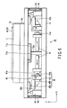
- the prober 10 can have a stage 1 whereon a wafer W is placed, a first horizontal driving mechanism 17 which supports the stage 1 and moves the stage 1 in the horizontal direction, an elevating mechanism 14 to move the stage 1 in the vertical direction, and alignment mechanisms 5a and 5b.
- the prober 10 can also have a rotary mechanism 1a to rotate the stage 1.
- the elevating mechanism 14 can include a first elevating mechanism 18 and second elevating mechanism 19.
- the first horizontal driving mechanism 17 can have a Y table 13 which moves in the Y direction, and an X table 12 which is arranged on the Y table and moves in the X direction.
- the first horizontal driving mechanism 17 can move the stage 1 in the X and Y directions in a prober chamber 15.
- the first elevating driving mechanism 18 moves the stage 1 upward in the Z direction, to bring the wafer W on the stage 1 into electrical contact with probes 16a of a probing card 16 arranged above the wafer W. In this state, a tester 7 tests the electrical characteristics of the integrated circuits on the wafer W.
- the X table 12 can reciprocate along a pair of X-direction guide rails 12a arranged on the Y table 13.
- the Y table 13 can reciprocate along a pair of Y-direction guide rails 13a arranged on a support plate 18a.
- the X and Y tables 12 and 13 are connected to motors (AC servo motors or the like) 2d and 3d (see FIG. 7) through ball screws 2a and 3a (see FIG. 7) in the same manner as in the prior art.
- motors rotate the ball screws
- the X and Y tables move in the X and Y directions.
- the X and Y tables 12 and 13 move the stage 1 in the X and Y directions within a horizontal plane.
- the two tables 12 and 13 as a whole will be referred to as the first horizontal driving mechanism 17 when necessary.
- the first horizontal driving mechanism 17 can be any mechanism as far as it is a mechanism that moves the stage 1 in the horizontal direction.
- the first horizontal driving mechanism 17 can be a mechanism based on a linear driving principle.
- the elevating mechanism 14 is divided into the first elevating mechanism 18 and second elevating mechanism 19, as shown in FIG. 1.
- the second elevating mechanism 19 is made lightweight, and the speed of the first horizontal driving mechanism 17 can be increased.
- the first elevating mechanism 18 supports the first horizontal driving mechanism 17 and stage 1 by its support plate 18a, and vertically moves them integrally.
- the second elevating mechanism 19 can be arranged on the first horizontal driving mechanism 17.
- the second elevating mechanism 19 vertically moves the stage 1.
- the first elevating mechanism 18 can vertically move the stage 1 over a long distance (e.g., 20 to 50 mm) when performing alignment or moving the stage 1 close to the probing card 16.
- the second elevating mechanism 19 can vertically move the stage 1 over a short distance (e.g., several hundred ⁇ m) when, e.g., bringing the probes 16a of the probing card 16 into contact with, or separating them from, the electrode pads of an object P to be tested after alignment.
- the first elevating mechanism 18 can also control the inclination of the stage 1 such that a stage surface 1b of the stage 1 becomes parallel to the probing card 16.
- the stage 1 is supported by the first horizontal driving mechanism 17, and the first horizontal driving mechanism 17 is arranged on the support plate 18a of the first elevating mechanism 18.
- the support plate 18a can have nut members 18b attached to its four corners, ball screws 18c which threadably engage with the corresponding nut members 18b, motors (e.g., AC servo motors) 18d connected to the corresponding ball screws 18c, and guide rails 18e which guide the support plate 18a in the Z direction.
- motors e.g., AC servo motors
- the ball screws 18c can support the support plate 18a at four points and vertically move the support plate 18a. Even when a large contact load is applied to the stage 1 from the probes 16a, the support plate 18a is not likely to be inclined. The stage 1 is also not likely to be inclined.
- the first elevating member 14' can support the support plate 18a through a rotary support mechanism (e.g., ball joint) 18j.
- a rotary support mechanism e.g., ball joint
- the support plate 18a indicated by a broken line in FIG. 8 is inclined. In the inclined state as well, the support plate 18a can be smoothly supported by the first elevating means 14, which moves in the vertical direction, through the rotary support mechanism 18j.
- FIG. 9 shows a ball joint 18j as an example of the rotary support mechanism 18j.
- the ball joint 18j can include a stationary portion 18k, spherical hole 18p in the stationary portion 18k, ball bearings 18m, support column 18n, and sphere 181 provided to the head of the support column 18n.
- the ball joint 18j can be fixed to the lower portion of the support plate 18a through the stationary portion 18k.
- the sphere 181 can freely rotate in the spherical hole 18p through the ball bearings.
- the inclined support plate 18a can be smoothly supported by the support column 18n of the first elevating means 14 through rotation of the sphere 181.
- a support plate 18f having an opening at its center may be used, as shown in FIG. 3.
- a scale 18g arranged above either guide rail 18e, and a detector 18h for detecting the gradations of the scale 18g can also measure the elevating amount of the stage 1.
- the second elevating mechanism 19 can have a plurality of (e.g., 3 or 4) linear-direction driving members (e.g., piezoelectric effect elements or piezo elements) 19b arranged equidistantly and having a piezoelectric effect.
- the linear-direction driving members 19b support the stage 1 through a support 19a.
- the stage 1 can be vertically moved over a short distance (e.g., 200 to 500 ⁇ m) in directions indicated by arrows in FIG. 2.
- the X table 12 can be provided with elevation detectors 19c which detect the elevation distance of the stage 1.
- elevation detector 19c a laser displacement sensor, electrostatic capacitance sensor, or the like can be employed.
- the elevation distance of the stage 1 can be controlled on the basis of the detection values of the elevation detectors 19c.
- the linear-direction driving member 19b a mechanism that uses a motor and ball screw can also be employed.
- the linear-direction driving member 19b using a piezoelectric element 19b can generate a driving force larger than that generated by the mechanism that uses the motor and ball screw.
- the voltages to be applied to the piezoelectric elements 19b are controlled, the small expanding/contracting amounts of the piezoelectric elements can be controlled at high speed and with high accuracy.
- the individual piezoelectric elements 19b can be controlled. Thus, when a contact load nonuniformly acts on the peripheral portion of the stage 1, the stage 1 can be kept horizontal by controlling the individual piezoelectric elements 19b.
- the stage 1 can be made lightweight.
- the stage 1 can be horizontally moved at high speed by the first horizontal driving mechanism 17.
- the angle of inclination of the stage 1 is adjusted by the first elevating mechanism 18 such that the stage surface 1b of the stage 1 becomes parallel to the distal end position of the predetermined probe among the plurality of probes 16a of the probing card 16 arranged above the stage.
- FIGS. 4A and 4B are graphs for comparing the elevation speed of the wafer W on the stage 1 when the piezoelectric elements 19b of the second elevating mechanism 19 are used and the elevation speed of the stage 1 when conventional ball screws are used. Referring to FIGS. 4A and 4B, (1) indicates the elevation speed of the stage 1; and (2), the upward moving distance of the stage 1 (wafer).
- the stage driving apparatus 9 of the prober 10 has the stage 1 for placing the wafer W thereon, the first horizontal driving mechanism 17 for moving the stage 1 in the horizontal direction, and the elevating driving mechanism 14 for moving the stage 1 in the vertical direction.
- the elevating mechanism 14 can include the first elevating mechanism 18 and second elevating mechanism 19.
- the first elevating mechanism 18 supports the first horizontal driving mechanism 17 and vertically moves it.
- the second elevating mechanism 19 is placed on the first horizontal driving mechanism 17, and supports the stage 1 and vertically moves it a short distance. Consequently, even if the probing card 16 varies and the contact load increases, the weight of the second elevating mechanism 19 for probing need not be increased.
- the first horizontal driving mechanism 17 can be driven at high speed. High-speed testing can be realized by drive-controlling the stage 1 at high speed.
- the support plate 18a of the first elevating mechanism 18 can be supported at its four corners such that it can move vertically. Even when a nonuniform load from the probes 16a acts on the wafer W on the stage 1, the support plate 18a will not be inclined.
- the stage 1 can be supported at a plurality of (e.g., 3 or 4) portions.
- the stage 1 will not likely to be inclined by the nonuniform load from the probes 16a. Even if the stage 1 may be inclined, its inclination can be prevented by controlling the elevation amounts of the piezoelectric elements 19b individually.
- the second elevating mechanism 19 can support the stage 1 through the plurality (e.g., 3 or 4) of piezoelectric elements 19b arranged equidistantly.
- the stage 1 can be driven at high speed over a short distance. Consequently, the test speed can be further increased, and the rigidity of the stage 1 itself can be increased.
- FIG. 5 schematically shows a second elevating mechanism 19 according to another embodiment of the present invention.
- a stage driving apparatus 9 of this embodiment can be configured in the same manner as in the above embodiment except for the second elevating mechanism 19.
- the second elevating mechanism 19 of this embodiment has, below the outer periphery of a stage 1, second horizontal driving mechanisms 30 (e.g., mechanisms having piezoelectric elements 31 exhibiting a piezoelectric effect) arranged horizontally at three locations equidistantly in the circumferential direction, and direction switching means 32 for converting expansion/contraction of the piezoelectric elements 31 into movement in the vertical direction.
- the stage 1 can be elevated a predetermined distance by controlling the expanding/contracting amounts of the respective piezoelectric elements 31.
- the direction switching means 32 of this embodiment has a first wedge member 31a, under the lower surface of the stage 1, which can move forward and backward and has a first inclined surface 31b inclined downward from the outer side toward the inner side in the radial direction, and a second wedge member 32a arranged to oppose the first inclined surface 31b through a ball bearing 32c.
- the second wedge member 32a has a second inclined surface 32b.
- Each first wedge member 31a is connected to one end of the corresponding piezoelectric element 31.
- the other end of the piezoelectric element 31 can be fixed to a corresponding stationary portion 33 arranged on an X table 12.
- the stationary portion 33 can be provided with elevation detectors 34 (e.g., laser displacement sensors or electrostatic capacitance sensors) which detect the elevation distance of the stage 1.
- the elevation distance of the stage 1 can be controlled on the basis of the detection values of the elevation detectors 34.
- the piezoelectric elements 31 at three locations are expanded or contracted in directions indicated by arrows X in FIG. 5 under the control of a controller 11 on the basis of the detection values of the elevation detectors 34, to move the first wedge members 31a forward/backward in the radial direction.
- the stage 1 can be vertically moved as indicated by arrows Z in FIG. 5 through the first inclined surfaces 31b of the first wedge members 31a, the second inclined surfaces 32b, and ball bearings 32c.
- a function and effect similar to those of the above embodiment can be expected.
- FIG. 6 is a view schematically showing a second elevating mechanism 40 according to still another embodiment of the present invention.
- the prober of this embodiment can be configured in the same manner as the respective embodiments described above except for the second elevating mechanism 40.
- a second elevating mechanism 40 can have piezoelectric elements 41 (e.g., at three locations) which are horizontally arranged radially from a central portion below a stage 1 and have a piezoelectric effect, and direction switching means 42 (e.g., at three locations) which convert the expanding/contracting forces of the piezoelectric elements 41 into movement in the vertical direction.
- the stage 1 can be vertically moved a predetermined distance.
- a leaf spring 11b can be arranged at the central portion of the lower surface of the stage 1 through spacers 11a.
- a support column 12a vertically extending from the center of an X table 12 is in contact with the leaf spring 11b.
- the direction switching means 42 of this embodiment can have an L-shaped turning member 42b a distal end 42e of which comes into contact with the peripheral portion of the lower surface of the stage 1 through a ball bearing 42a, and a support member 42c which axially supports the turning member 42b such that the turning member 42b can turn.
- the other end of the L-shaped turning member 42b engages with an engaging portion 41a at one end of the corresponding piezoelectric element 41 through a ball bearing 42d.
- the turning member 42b can serve to convert expansion and contraction in the horizontal direction of the piezoelectric element 41 into movement in the vertical direction and amplify the expanding/contracting amount of the piezoelectric element 41. Consequently, the stage 1 can elevate by an elevating amount larger than the expanding/contracting amount of the piezoelectric element 41.
- Elevation detectors 43 e.g., laser displacement sensors or electrostatic capacitance sensors which detect the elevation distance of the stage 1 can be arranged outside the turning members 42b.
- the elevation distance of the stage 1 can be controlled on the basis of the elevation distances of the respective portions detected by the elevation detectors 43.
- the expanding/contracting amounts of the piezoelectric elements 41 can be controlled on the basis of the detection values, to horizontally control the stage 1.
- Springs 44 which connect the stage 1 and X table 12 such that the springs 44 can expand and contract can be arranged further outside the elevation detectors 43.
- the springs 44 can restore the stage 1, that has moved upward, to the initial state quickly.
- the stage 1 can be vertically moved by an amount larger than the expanding/contracting amount of the piezoelectric elements 41.
- the direction switching means may be arranged to correspond to the second horizontal driving mechanisms. Accordingly, the direction switching means need not always be arranged equidistantly in the circumferential direction of the stage 1, and the number of direction switching means is not limited to three.
- the elevation detectors can be omitted.
- the second inclined surfaces 32b at three locations may be formed in an integral member as passages for the wedge members.
- the object P to be tested is not limited to a wafer, but can be an LCD substrate or IC chip.
- a stage driving apparatus 9 and a probe method which, even when the contact load increases as the probing card 16 varies, can drive-control the stage 1 at high speed to realize high-speed testing.
Landscapes
- Engineering & Computer Science (AREA)
- General Engineering & Computer Science (AREA)
- Physics & Mathematics (AREA)
- General Physics & Mathematics (AREA)
- Computer Hardware Design (AREA)
- Microelectronics & Electronic Packaging (AREA)
- Testing Or Measuring Of Semiconductors Or The Like (AREA)
- General Electrical Machinery Utilizing Piezoelectricity, Electrostriction Or Magnetostriction (AREA)
- Container, Conveyance, Adherence, Positioning, Of Wafer (AREA)
- Testing Of Individual Semiconductor Devices (AREA)
- Measuring Leads Or Probes (AREA)
- Tests Of Electronic Circuits (AREA)
- Investigating Or Analyzing Materials By The Use Of Ultrasonic Waves (AREA)
- Analysing Materials By The Use Of Radiation (AREA)
- Maintenance And Management Of Digital Transmission (AREA)
- Liquid Crystal Substances (AREA)
Abstract
Description
Claims (11)
- A stage driving apparatus (9) formed to move a stage (1) having a substrate (W) to be tested on a stage surface (1b) thereof in horizontal and vertical directions, the stage driving apparatus comprising:a second elevating mechanism (19) configured to support the stage and move the stage in the vertical direction;a first horizontal driving mechanism (17) configured to support the second elevating mechanism and move the second elevating mechanism in X and Y directions on a horizontal plane; anda first elevating mechanism (18) configured to support the first horizontal driving mechanism and move the first horizontal driving mechanism in the vertical direction.
- A stage driving apparatus according to claim 1, wherein the second elevating mechanism has a plurality of linear-direction driving members (19), the plurality of linear-direction driving members being configured to support the stage at a plurality of portions and move the stage in the vertical direction.
- A stage driving apparatus according to claim 2, wherein the linear-direction driving members include one of a piezoelectric-effect member and a ball screw (33).
- A stage driving apparatus according to claim 1, wherein the second elevating mechanism has at least one second horizontal driving mechanism (30) which generates a driving force in the horizontal direction, and at least one direction switching unit (32) which converts the horizontal-direction driving force of the second horizontal driving mechanism into a driving force in the vertical direction.
- A stage driving apparatus according to claim 4, wherein the direction switching unit includes:a first wedge member (31a) arranged on the first horizontal driving member to be movable, the first wedge member being moved forward/backward in the horizontal direction by the horizontal-direction driving force of the second horizontal driving mechanism; anda second wedge member (32a) fixed to a lower portion of the stage, andthe first wedge member is arranged to oppose the second wedge member, and moved forward/backward in the horizontal direction by the horizontal-direction driving force of the second horizontal driving mechanism, to move the second wedge member, thus moving the stage in the vertical direction.
- A stage driving apparatus according to claim 4, wherein the direction switching unit includes:a turning member (42b) which is turned by the horizontal-direction driving force of the second horizontal driving mechanism (30), a distal end (42e) of the turning member coming into contact with a lower portion of the stage, and the turning member turning to move the stage in the vertical direction; anda support member (42c) which supports the turning member to be turnable.
- A stage driving apparatus according to claim 1, wherein the first elevating mechanism (18) includes at least one first elevating means (14) having a support (18a) which supports the first horizontal driving mechanism (17) and can move in the vertical direction, a guide member (18e) which guides movement in the vertical direction of the support, and a ball screw (18c) and motor (18d) configured to vertically move the support along the guide member.
- A stage driving apparatus according to claim 1, wherein the first elevating mechanism serves, in addition to moving the first horizontal driving mechanism in the vertical direction, to adjust an angle of inclination of the stage such that the stage surface (1b) of the stage becomes parallel to a probing card (16) arranged above the stage.
- A stage driving apparatus according to claim 8, wherein the first elevating mechanism (18) includes a plurality of first elevating members (14) (18b, 18d, and 18c), each of the first elevating members being configured to support the first horizontal driving mechanism through a rotary support mechanism (18j) and move the first horizontal driving mechanism in the vertical direction.
- In a prober comprising a tester (7) and stage, a probe method of testing electrical characteristics of an object (P) to be tested on a substrate (W) to be tested, the probe method comprising:(a1) placing the substrate to be tested on a stage surface (1b) of the stage (1);(a2) detecting a position of the object to be tested formed on the substrate to be tested and a position of a predetermined probe among a plurality of probes of a probing card arranged above the stage;(a3) moving the stage in X, Y, and Z directions to align the object to be tested on the substrate to be tested on the stage and the probes (16a) of the probing card (16) arranged on the stage;(a4) moving the stage upward by the first elevating mechanism toward the probing card, such upward moving not bringing the object to be tested on the stage into contact with the plurality of probes of the probing card;(a5) over-driving the stage toward the probes by the second elevating mechanism (19);(a6) testing the electrical characteristics of the object to be tested with a tester (7);(a7) after testing, moving the stage downward by the second elevating mechanism to separate the object to be tested from the probes;(a8) indexing the stage by the horizontal driving mechanism, such indexing serving to move the next object to be tested to a position immediately below the probes of the probing card; and(a9) repeating (a5) to (a8) to test the electrical characteristics of a predetermined object to be tested on the substrate to be tested.
- A probe method according to claim 10 comprising, after position detection of (a2), performing the following (a2'):(a2') adjusting an angle of inclination of the stage by the first elevating mechanism such that the stage surface of the stage becomes parallel to a position of a distal end of a predetermined probe among the probes (16a) of the probing card (16) arranged above the stage.
Applications Claiming Priority (3)
| Application Number | Priority Date | Filing Date | Title |
|---|---|---|---|
| JP2002230563 | 2002-08-07 | ||
| JP2002230563A JP4300003B2 (en) | 2002-08-07 | 2002-08-07 | Mounting table driving apparatus and probe method |
| PCT/JP2003/009879 WO2004015434A1 (en) | 2002-08-07 | 2003-08-04 | Placing table drive device and probe method |
Publications (3)
| Publication Number | Publication Date |
|---|---|
| EP1538452A1 true EP1538452A1 (en) | 2005-06-08 |
| EP1538452A4 EP1538452A4 (en) | 2005-10-26 |
| EP1538452B1 EP1538452B1 (en) | 2006-11-22 |
Family
ID=31711688
Family Applications (1)
| Application Number | Title | Priority Date | Filing Date |
|---|---|---|---|
| EP03784514A Expired - Lifetime EP1538452B1 (en) | 2002-08-07 | 2003-08-04 | Stage driving apparatus and probe method |
Country Status (9)
| Country | Link |
|---|---|
| US (1) | US7106082B2 (en) |
| EP (1) | EP1538452B1 (en) |
| JP (1) | JP4300003B2 (en) |
| KR (1) | KR100724169B1 (en) |
| CN (1) | CN100397091C (en) |
| AT (1) | ATE346311T1 (en) |
| DE (1) | DE60309892T2 (en) |
| TW (1) | TW200406865A (en) |
| WO (1) | WO2004015434A1 (en) |
Cited By (1)
| Publication number | Priority date | Publication date | Assignee | Title |
|---|---|---|---|---|
| CN101762755B (en) * | 2008-12-24 | 2012-03-21 | 深圳麦逊电子有限公司 | High-density printed circuit board (PCB) test machine and method |
Families Citing this family (66)
| Publication number | Priority date | Publication date | Assignee | Title |
|---|---|---|---|---|
| DE602005026141D1 (en) * | 2004-05-20 | 2011-03-10 | Japan Science & Tech Agency | Method and device for precise and high load-resistant movement |
| KR100679317B1 (en) | 2004-09-01 | 2007-02-07 | 노우철 | LC-driven IC's inspection aid |
| CN100360943C (en) * | 2004-11-29 | 2008-01-09 | 华硕电脑股份有限公司 | Testing device capable of preventing excessive pressure |
| JP4489639B2 (en) * | 2005-05-31 | 2010-06-23 | 住友重機械工業株式会社 | Z-axis adjustment mechanism and fine movement stage device |
| JP2007147536A (en) * | 2005-11-30 | 2007-06-14 | Tokyo Electron Ltd | Probe card transfer assist device and inspection equipment |
| JP4878918B2 (en) * | 2006-05-30 | 2012-02-15 | 株式会社東京精密 | Prober and probing method |
| JP4965273B2 (en) * | 2007-02-02 | 2012-07-04 | 東京エレクトロン株式会社 | Mounting device |
| KR100807090B1 (en) * | 2007-03-28 | 2008-02-26 | 에스엔유 프리시젼 주식회사 | Substrate support device and seal pattern inspection device of LCD cell |
| JP4999615B2 (en) * | 2007-08-31 | 2012-08-15 | 東京エレクトロン株式会社 | Inspection apparatus and inspection method |
| KR100936631B1 (en) * | 2007-11-22 | 2010-01-14 | 주식회사 쎄믹스 | Coaxial axis position control device and method of wafer prober |
| WO2009072194A1 (en) * | 2007-12-05 | 2009-06-11 | Sumitomo Metal Industries, Ltd. | Process for manufacturing metal pipe with extremely thin wall by cold rolling |
| US8819743B2 (en) | 2007-12-19 | 2014-08-26 | Dish Network L.L.C. | Transfer of data related to broadcast programming over a communication network |
| JP2009164298A (en) * | 2007-12-28 | 2009-07-23 | Tokyo Electron Ltd | Inclination adjusting device and probe device of mounting body |
| CN101303532B (en) * | 2008-06-10 | 2010-06-09 | 上海微电子装备有限公司 | Six-degree-of-freedom precision positioning table with switchable stations |
| US9337545B2 (en) | 2008-06-20 | 2016-05-10 | Dish Network L.L.C. | Apparatus and systems for mounting an electrical switching device |
| US8907862B2 (en) | 2011-04-12 | 2014-12-09 | Dish Network L.L.C. | Apparatus and systems for mounting an electrical switching device |
| WO2009157037A1 (en) * | 2008-06-24 | 2009-12-30 | アキム株式会社 | Electronic component inspection apparatus and electronic component inspection system |
| JP5406480B2 (en) * | 2008-08-08 | 2014-02-05 | 東京エレクトロン株式会社 | Probe method and probe program |
| CN101665923A (en) * | 2008-09-04 | 2010-03-10 | 东京毅力科创株式会社 | Film deposition apparatus, substrate processing apparatus and film deposition method |
| JP5280964B2 (en) * | 2008-09-04 | 2013-09-04 | 東京エレクトロン株式会社 | Film forming apparatus, substrate processing apparatus, film forming method, and storage medium |
| JP5289898B2 (en) * | 2008-11-07 | 2013-09-11 | 住友重機械工業株式会社 | Stage device and prober device |
| KR101583000B1 (en) * | 2009-03-09 | 2016-01-19 | 삼성전자주식회사 | Apparatus and method for testing semiconductor device |
| TWI384227B (en) * | 2009-09-01 | 2013-02-01 | Advanced Semiconductor Eng | Active non-contact probe card |
| JP5384270B2 (en) * | 2009-09-21 | 2014-01-08 | 東京エレクトロン株式会社 | loader |
| US8462075B2 (en) * | 2010-02-23 | 2013-06-11 | Dish Network L.L.C. | Apparatus for mounting an object to a railing |
| WO2011138938A1 (en) * | 2010-05-07 | 2011-11-10 | Nskテクノロジー株式会社 | Supporting device and light exposure device |
| JP5517350B2 (en) | 2010-06-15 | 2014-06-11 | 東京エレクトロン株式会社 | Mounting table drive device |
| KR101052506B1 (en) * | 2010-06-16 | 2011-07-29 | 주식회사 이노비즈 | LED inspection device and LED inspection method using the same |
| JP5826466B2 (en) * | 2010-06-25 | 2015-12-02 | 東京エレクトロン株式会社 | Probe card parallel adjustment mechanism and inspection device |
| US8646186B2 (en) | 2010-12-16 | 2014-02-11 | Dish Network L.L.C. | Multi-angle levels and plumbing methods |
| US8802985B2 (en) | 2011-09-07 | 2014-08-12 | Dish Network L.L.C. | In-wall extension apparatus |
| JP6040530B2 (en) * | 2012-01-17 | 2016-12-07 | セイコーエプソン株式会社 | Handler and inspection equipment |
| US9123987B2 (en) | 2012-07-31 | 2015-09-01 | Dish Network L.L.C. | Antenna mounting systems and methods |
| CN102944791A (en) * | 2012-11-15 | 2013-02-27 | 昆山迈致治具科技有限公司 | Test fixture with automatic marking function |
| JP5978992B2 (en) * | 2012-12-28 | 2016-08-24 | 株式会社ソシオネクスト | Electronic device test apparatus and test method |
| TW201334095A (en) * | 2013-04-18 | 2013-08-16 | Hauman Technologies Corp | Probing device with three-directional motion |
| JP6293499B2 (en) * | 2014-01-27 | 2018-03-14 | 株式会社日立ハイテクノロジーズ | Vacuum processing equipment |
| CN103941117B (en) * | 2014-03-14 | 2016-04-06 | 上海交通大学 | Electrical transport measurement mechanism and measuring method |
| EP2927948A1 (en) | 2014-04-04 | 2015-10-07 | Nordson Corporation | X-ray inspection apparatus for inspecting semiconductor wafers |
| KR101611922B1 (en) * | 2014-05-12 | 2016-04-14 | 참엔지니어링(주) | Apparatus and method for testing a substrate |
| CN105181157B (en) * | 2014-06-20 | 2017-07-28 | 沈阳芯源微电子设备有限公司 | A kind of thermometric wafer micromatic setting |
| TWI573700B (en) * | 2015-02-13 | 2017-03-11 | rong-gui Deng | Assembly equipment for loading equipment and its applications |
| JP6437884B2 (en) * | 2015-06-03 | 2018-12-12 | 旭化成エンジニアリング株式会社 | Planar moving device |
| JP6652361B2 (en) * | 2015-09-30 | 2020-02-19 | 東京エレクトロン株式会社 | Wafer inspection apparatus and wafer inspection method |
| KR102534364B1 (en) * | 2015-12-02 | 2023-05-18 | 세메스 주식회사 | Probe apparatus and method of setting zero point of the probe apparatus |
| TWI595865B (en) * | 2016-08-23 | 2017-08-21 | Hiwin Tech Corp | Equipped with a linear drive system inside the prosthesis |
| KR20190052533A (en) | 2017-11-08 | 2019-05-16 | 삼성전자주식회사 | Substrate supporting and transferring apparatus, method of supporting and transferring substrate, and manufacturing method of display apparatus using the same |
| US10510573B2 (en) * | 2017-11-14 | 2019-12-17 | Taiwan Semiconductor Manufacturing Co., Ltd. | Loading apparatus and operating method thereof |
| US11262380B2 (en) | 2018-01-19 | 2022-03-01 | Semics Inc. | Wafer prober |
| CN108646395A (en) * | 2018-05-04 | 2018-10-12 | 江苏羿骏自动化科技有限公司 | A kind of multistation mobile model microscope inspection measurement equipment |
| TWI676031B (en) * | 2018-09-06 | 2019-11-01 | 致茂電子股份有限公司 | Sliding test device for electronic component |
| CN109307631A (en) * | 2018-11-21 | 2019-02-05 | 广州提爱思汽车内饰系统有限公司 | A kind of leather stiffness and softness testing device and leather leather stiffness and softness intelligent testing method |
| US20210139314A1 (en) * | 2019-11-07 | 2021-05-13 | Innovative Interface Laboratory Corp. | Linear actuator |
| CN110919697B (en) * | 2019-12-10 | 2024-09-20 | 江苏敦邦钢结构工程有限公司 | Steel plate cutting deviation correcting device for assembled steel structure building |
| CN111208058B (en) * | 2020-03-05 | 2024-09-13 | 中华人民共和国吴江海关 | Device and method for detecting electrolyte holding capacity of storage battery |
| JP7597462B2 (en) * | 2020-11-16 | 2024-12-10 | 東京エレクトロン株式会社 | Substrate holding mechanism and substrate mounting method |
| CN112505373B (en) * | 2020-12-17 | 2025-05-13 | 广东柏兹电子科技有限公司 | An air-floating adjustment probe station |
| CN112763950A (en) * | 2020-12-22 | 2021-05-07 | 扬州京柏自动化科技有限公司 | Magnetic circuit testing device |
| CN112873137B (en) * | 2020-12-29 | 2022-11-04 | 北京半导体专用设备研究所(中国电子科技集团公司第四十五研究所) | Stripping workbench |
| CN112873227B (en) * | 2021-01-20 | 2022-11-15 | 北京半导体专用设备研究所(中国电子科技集团公司第四十五研究所) | Carrying manipulator and laminating device |
| CN115490020A (en) * | 2021-06-17 | 2022-12-20 | 南通中集特种运输设备制造有限公司 | Loading device and loading method for integrated equipment |
| US12354898B2 (en) * | 2021-09-30 | 2025-07-08 | Tokyo Electron Limited | Stage, testing apparatus, and stage operating method |
| JP2023051734A (en) * | 2021-09-30 | 2023-04-11 | 東京エレクトロン株式会社 | Stage, inspection device, and stage operating method |
| CN114720371B (en) * | 2022-04-12 | 2023-01-06 | 广东雷诺精密科技有限公司 | Dial stone adhesion quality testing device and method |
| JP2023167818A (en) * | 2022-05-13 | 2023-11-24 | 株式会社アドバンテスト | Electronic component handling device and electronic component test device |
| CN117583657B (en) * | 2024-01-19 | 2024-03-26 | 无锡七机机床有限公司 | High-precision planing and thinning machine tool adjusting device |
Family Cites Families (8)
| Publication number | Priority date | Publication date | Assignee | Title |
|---|---|---|---|---|
| KR100248569B1 (en) * | 1993-12-22 | 2000-03-15 | 히가시 데쓰로 | Probe system |
| JP3094056B2 (en) * | 1994-05-24 | 2000-10-03 | 東京エレクトロン株式会社 | Probe device |
| JPH09330960A (en) * | 1996-06-08 | 1997-12-22 | Tokyo Electron Ltd | Inspection device |
| JPH11111787A (en) * | 1997-10-03 | 1999-04-23 | Eejingu Tesuta Kaihatsu Kyodo Kumiai | Wafer inspection equipment |
| JPH11251379A (en) * | 1998-02-27 | 1999-09-17 | Toshiba Microelectronics Corp | Wafer probing equipment |
| JP2000260852A (en) * | 1999-03-11 | 2000-09-22 | Tokyo Electron Ltd | Inspection stage and inspection device |
| JP2001358204A (en) * | 2000-06-15 | 2001-12-26 | Tokyo Electron Ltd | Inspection stage |
| JP4659328B2 (en) * | 2002-10-21 | 2011-03-30 | 東京エレクトロン株式会社 | Probe device for controlling the temperature of an object to be inspected |
-
2002
- 2002-08-07 JP JP2002230563A patent/JP4300003B2/en not_active Expired - Lifetime
-
2003
- 2003-08-04 KR KR1020047019856A patent/KR100724169B1/en not_active Expired - Fee Related
- 2003-08-04 DE DE60309892T patent/DE60309892T2/en not_active Expired - Lifetime
- 2003-08-04 CN CNB038139251A patent/CN100397091C/en not_active Expired - Fee Related
- 2003-08-04 AT AT03784514T patent/ATE346311T1/en not_active IP Right Cessation
- 2003-08-04 WO PCT/JP2003/009879 patent/WO2004015434A1/en not_active Ceased
- 2003-08-04 EP EP03784514A patent/EP1538452B1/en not_active Expired - Lifetime
- 2003-08-07 TW TW092121692A patent/TW200406865A/en not_active IP Right Cessation
-
2005
- 2005-01-25 US US11/041,284 patent/US7106082B2/en not_active Expired - Lifetime
Cited By (1)
| Publication number | Priority date | Publication date | Assignee | Title |
|---|---|---|---|---|
| CN101762755B (en) * | 2008-12-24 | 2012-03-21 | 深圳麦逊电子有限公司 | High-density printed circuit board (PCB) test machine and method |
Also Published As
| Publication number | Publication date |
|---|---|
| WO2004015434A1 (en) | 2004-02-19 |
| EP1538452A4 (en) | 2005-10-26 |
| TW200406865A (en) | 2004-05-01 |
| US20050127898A1 (en) | 2005-06-16 |
| US7106082B2 (en) | 2006-09-12 |
| EP1538452B1 (en) | 2006-11-22 |
| DE60309892T2 (en) | 2007-06-21 |
| KR100724169B1 (en) | 2007-05-31 |
| ATE346311T1 (en) | 2006-12-15 |
| DE60309892D1 (en) | 2007-01-04 |
| JP2004071909A (en) | 2004-03-04 |
| TWI302010B (en) | 2008-10-11 |
| JP4300003B2 (en) | 2009-07-22 |
| KR20050004293A (en) | 2005-01-12 |
| CN1662821A (en) | 2005-08-31 |
| CN100397091C (en) | 2008-06-25 |
Similar Documents
| Publication | Publication Date | Title |
|---|---|---|
| EP1538452B1 (en) | Stage driving apparatus and probe method | |
| CN111566798B (en) | chip detector | |
| JP5664938B2 (en) | Prober and probe inspection method | |
| CN115274484B (en) | Wafer detection device and detection method thereof | |
| JP5987967B2 (en) | Probing apparatus and probe contact method | |
| JPH0613416A (en) | Die bonding machine | |
| WO2007089543A2 (en) | Active probe contact array management | |
| WO1996030772A1 (en) | Interface apparatus for automatic test equipment | |
| US6707310B2 (en) | Needle load measuring method, needle load setting method and needle load detecting mechanism | |
| JP5747428B2 (en) | Positioning and fixing device | |
| JP4175086B2 (en) | Wafer support apparatus for inspection and wafer support method for inspection | |
| JP3902747B2 (en) | Probe device | |
| CN118707276A (en) | A method and device for controlling the distance between a probe of a detector and a wafer | |
| KR102936377B1 (en) | Surface contamination inspection equipment equipped with a wafer stage | |
| JP7773800B2 (en) | Workpiece holding mechanism, workpiece processing device, and workpiece holding method | |
| US20240300113A1 (en) | Substrate positioning device, substrate positioning method, and bonding apparatus | |
| JP2022082170A (en) | Method for reducing prober power consumption and prober | |
| JP2025072918A (en) | Moving device, inspection device, and moving method |
Legal Events
| Date | Code | Title | Description |
|---|---|---|---|
| PUAI | Public reference made under article 153(3) epc to a published international application that has entered the european phase |
Free format text: ORIGINAL CODE: 0009012 |
|
| 17P | Request for examination filed |
Effective date: 20050307 |
|
| AK | Designated contracting states |
Kind code of ref document: A1 Designated state(s): AT BE BG CH CY CZ DE DK EE ES FI FR GB GR HU IE IT LI LU MC NL PT RO SE SI SK TR |
|
| A4 | Supplementary search report drawn up and despatched |
Effective date: 20050908 |
|
| RIC1 | Information provided on ipc code assigned before grant |
Ipc: 7G 01R 31/28 B Ipc: 7G 01R 31/319 A |
|
| GRAP | Despatch of communication of intention to grant a patent |
Free format text: ORIGINAL CODE: EPIDOSNIGR1 |
|
| RTI1 | Title (correction) |
Free format text: STAGE DRIVING APPARATUS AND PROBE METHOD |
|
| GRAS | Grant fee paid |
Free format text: ORIGINAL CODE: EPIDOSNIGR3 |
|
| GRAA | (expected) grant |
Free format text: ORIGINAL CODE: 0009210 |
|
| AK | Designated contracting states |
Kind code of ref document: B1 Designated state(s): AT BE BG CH CY CZ DE DK EE ES FI FR GB GR HU IE IT LI LU MC NL PT RO SE SI SK TR |
|
| PG25 | Lapsed in a contracting state [announced via postgrant information from national office to epo] |
Ref country code: IT Free format text: LAPSE BECAUSE OF FAILURE TO SUBMIT A TRANSLATION OF THE DESCRIPTION OR TO PAY THE FEE WITHIN THE PRESCRIBED TIME-LIMIT;WARNING: LAPSES OF ITALIAN PATENTS WITH EFFECTIVE DATE BEFORE 2007 MAY HAVE OCCURRED AT ANY TIME BEFORE 2007. THE CORRECT EFFECTIVE DATE MAY BE DIFFERENT FROM THE ONE RECORDED. Effective date: 20061122 Ref country code: FI Free format text: LAPSE BECAUSE OF FAILURE TO SUBMIT A TRANSLATION OF THE DESCRIPTION OR TO PAY THE FEE WITHIN THE PRESCRIBED TIME-LIMIT Effective date: 20061122 Ref country code: CZ Free format text: LAPSE BECAUSE OF FAILURE TO SUBMIT A TRANSLATION OF THE DESCRIPTION OR TO PAY THE FEE WITHIN THE PRESCRIBED TIME-LIMIT Effective date: 20061122 Ref country code: SK Free format text: LAPSE BECAUSE OF FAILURE TO SUBMIT A TRANSLATION OF THE DESCRIPTION OR TO PAY THE FEE WITHIN THE PRESCRIBED TIME-LIMIT Effective date: 20061122 Ref country code: BE Free format text: LAPSE BECAUSE OF FAILURE TO SUBMIT A TRANSLATION OF THE DESCRIPTION OR TO PAY THE FEE WITHIN THE PRESCRIBED TIME-LIMIT Effective date: 20061122 Ref country code: CH Free format text: LAPSE BECAUSE OF FAILURE TO SUBMIT A TRANSLATION OF THE DESCRIPTION OR TO PAY THE FEE WITHIN THE PRESCRIBED TIME-LIMIT Effective date: 20061122 Ref country code: AT Free format text: LAPSE BECAUSE OF FAILURE TO SUBMIT A TRANSLATION OF THE DESCRIPTION OR TO PAY THE FEE WITHIN THE PRESCRIBED TIME-LIMIT Effective date: 20061122 Ref country code: LI Free format text: LAPSE BECAUSE OF FAILURE TO SUBMIT A TRANSLATION OF THE DESCRIPTION OR TO PAY THE FEE WITHIN THE PRESCRIBED TIME-LIMIT Effective date: 20061122 Ref country code: NL Free format text: LAPSE BECAUSE OF FAILURE TO SUBMIT A TRANSLATION OF THE DESCRIPTION OR TO PAY THE FEE WITHIN THE PRESCRIBED TIME-LIMIT Effective date: 20061122 Ref country code: SI Free format text: LAPSE BECAUSE OF FAILURE TO SUBMIT A TRANSLATION OF THE DESCRIPTION OR TO PAY THE FEE WITHIN THE PRESCRIBED TIME-LIMIT Effective date: 20061122 Ref country code: RO Free format text: LAPSE BECAUSE OF FAILURE TO SUBMIT A TRANSLATION OF THE DESCRIPTION OR TO PAY THE FEE WITHIN THE PRESCRIBED TIME-LIMIT Effective date: 20061122 |
|
| REG | Reference to a national code |
Ref country code: GB Ref legal event code: FG4D |
|
| REG | Reference to a national code |
Ref country code: CH Ref legal event code: EP |
|
| REG | Reference to a national code |
Ref country code: IE Ref legal event code: FG4D |
|
| REF | Corresponds to: |
Ref document number: 60309892 Country of ref document: DE Date of ref document: 20070104 Kind code of ref document: P |
|
| PG25 | Lapsed in a contracting state [announced via postgrant information from national office to epo] |
Ref country code: BG Free format text: LAPSE BECAUSE OF FAILURE TO SUBMIT A TRANSLATION OF THE DESCRIPTION OR TO PAY THE FEE WITHIN THE PRESCRIBED TIME-LIMIT Effective date: 20070222 Ref country code: SE Free format text: LAPSE BECAUSE OF FAILURE TO SUBMIT A TRANSLATION OF THE DESCRIPTION OR TO PAY THE FEE WITHIN THE PRESCRIBED TIME-LIMIT Effective date: 20070222 Ref country code: DK Free format text: LAPSE BECAUSE OF FAILURE TO SUBMIT A TRANSLATION OF THE DESCRIPTION OR TO PAY THE FEE WITHIN THE PRESCRIBED TIME-LIMIT Effective date: 20070222 |
|
| PG25 | Lapsed in a contracting state [announced via postgrant information from national office to epo] |
Ref country code: ES Free format text: LAPSE BECAUSE OF FAILURE TO SUBMIT A TRANSLATION OF THE DESCRIPTION OR TO PAY THE FEE WITHIN THE PRESCRIBED TIME-LIMIT Effective date: 20070305 |
|
| PG25 | Lapsed in a contracting state [announced via postgrant information from national office to epo] |
Ref country code: PT Free format text: LAPSE BECAUSE OF FAILURE TO SUBMIT A TRANSLATION OF THE DESCRIPTION OR TO PAY THE FEE WITHIN THE PRESCRIBED TIME-LIMIT Effective date: 20070423 |
|
| NLV1 | Nl: lapsed or annulled due to failure to fulfill the requirements of art. 29p and 29m of the patents act | ||
| ET | Fr: translation filed | ||
| REG | Reference to a national code |
Ref country code: CH Ref legal event code: PL |
|
| PLBE | No opposition filed within time limit |
Free format text: ORIGINAL CODE: 0009261 |
|
| STAA | Information on the status of an ep patent application or granted ep patent |
Free format text: STATUS: NO OPPOSITION FILED WITHIN TIME LIMIT |
|
| 26N | No opposition filed |
Effective date: 20070823 |
|
| GBPC | Gb: european patent ceased through non-payment of renewal fee |
Effective date: 20070804 |
|
| PG25 | Lapsed in a contracting state [announced via postgrant information from national office to epo] |
Ref country code: MC Free format text: LAPSE BECAUSE OF NON-PAYMENT OF DUE FEES Effective date: 20070831 Ref country code: GR Free format text: LAPSE BECAUSE OF FAILURE TO SUBMIT A TRANSLATION OF THE DESCRIPTION OR TO PAY THE FEE WITHIN THE PRESCRIBED TIME-LIMIT Effective date: 20070223 |
|
| PG25 | Lapsed in a contracting state [announced via postgrant information from national office to epo] |
Ref country code: IE Free format text: LAPSE BECAUSE OF NON-PAYMENT OF DUE FEES Effective date: 20070807 |
|
| PG25 | Lapsed in a contracting state [announced via postgrant information from national office to epo] |
Ref country code: GB Free format text: LAPSE BECAUSE OF NON-PAYMENT OF DUE FEES Effective date: 20070804 |
|
| PG25 | Lapsed in a contracting state [announced via postgrant information from national office to epo] |
Ref country code: EE Free format text: LAPSE BECAUSE OF FAILURE TO SUBMIT A TRANSLATION OF THE DESCRIPTION OR TO PAY THE FEE WITHIN THE PRESCRIBED TIME-LIMIT Effective date: 20061122 |
|
| PG25 | Lapsed in a contracting state [announced via postgrant information from national office to epo] |
Ref country code: CY Free format text: LAPSE BECAUSE OF FAILURE TO SUBMIT A TRANSLATION OF THE DESCRIPTION OR TO PAY THE FEE WITHIN THE PRESCRIBED TIME-LIMIT Effective date: 20061122 Ref country code: LU Free format text: LAPSE BECAUSE OF NON-PAYMENT OF DUE FEES Effective date: 20070804 |
|
| PG25 | Lapsed in a contracting state [announced via postgrant information from national office to epo] |
Ref country code: TR Free format text: LAPSE BECAUSE OF FAILURE TO SUBMIT A TRANSLATION OF THE DESCRIPTION OR TO PAY THE FEE WITHIN THE PRESCRIBED TIME-LIMIT Effective date: 20061122 Ref country code: HU Free format text: LAPSE BECAUSE OF FAILURE TO SUBMIT A TRANSLATION OF THE DESCRIPTION OR TO PAY THE FEE WITHIN THE PRESCRIBED TIME-LIMIT Effective date: 20070523 |
|
| PGFP | Annual fee paid to national office [announced via postgrant information from national office to epo] |
Ref country code: FR Payment date: 20090814 Year of fee payment: 7 |
|
| PGFP | Annual fee paid to national office [announced via postgrant information from national office to epo] |
Ref country code: DE Payment date: 20090730 Year of fee payment: 7 |
|
| REG | Reference to a national code |
Ref country code: FR Ref legal event code: ST Effective date: 20110502 |
|
| REG | Reference to a national code |
Ref country code: DE Ref legal event code: R119 Ref document number: 60309892 Country of ref document: DE Effective date: 20110301 |
|
| PG25 | Lapsed in a contracting state [announced via postgrant information from national office to epo] |
Ref country code: DE Free format text: LAPSE BECAUSE OF NON-PAYMENT OF DUE FEES Effective date: 20110301 Ref country code: FR Free format text: LAPSE BECAUSE OF NON-PAYMENT OF DUE FEES Effective date: 20100831 |